US10598798B2 - Radiation detector with an intermediate layer - Google Patents
Radiation detector with an intermediate layer Download PDFInfo
- Publication number
- US10598798B2 US10598798B2 US15/798,626 US201715798626A US10598798B2 US 10598798 B2 US10598798 B2 US 10598798B2 US 201715798626 A US201715798626 A US 201715798626A US 10598798 B2 US10598798 B2 US 10598798B2
- Authority
- US
- United States
- Prior art keywords
- radiation detector
- intermediate layer
- detection
- readout units
- readout
- Prior art date
- Legal status (The legal status is an assumption and is not a legal conclusion. Google has not performed a legal analysis and makes no representation as to the accuracy of the status listed.)
- Active
Links
Images


Classifications
-
- G—PHYSICS
- G01—MEASURING; TESTING
- G01T—MEASUREMENT OF NUCLEAR OR X-RADIATION
- G01T1/00—Measuring X-radiation, gamma radiation, corpuscular radiation, or cosmic radiation
- G01T1/02—Dosimeters
- G01T1/10—Luminescent dosimeters
- G01T1/11—Thermo-luminescent dosimeters
- G01T1/115—Read-out devices
-
- G—PHYSICS
- G01—MEASURING; TESTING
- G01T—MEASUREMENT OF NUCLEAR OR X-RADIATION
- G01T1/00—Measuring X-radiation, gamma radiation, corpuscular radiation, or cosmic radiation
- G01T1/29—Measurement performed on radiation beams, e.g. position or section of the beam; Measurement of spatial distribution of radiation
-
- G—PHYSICS
- G01—MEASURING; TESTING
- G01T—MEASUREMENT OF NUCLEAR OR X-RADIATION
- G01T1/00—Measuring X-radiation, gamma radiation, corpuscular radiation, or cosmic radiation
- G01T1/16—Measuring radiation intensity
- G01T1/20—Measuring radiation intensity with scintillation detectors
- G01T1/2002—Optical details, e.g. reflecting or diffusing layers
-
- G—PHYSICS
- G01—MEASURING; TESTING
- G01T—MEASUREMENT OF NUCLEAR OR X-RADIATION
- G01T1/00—Measuring X-radiation, gamma radiation, corpuscular radiation, or cosmic radiation
- G01T1/16—Measuring radiation intensity
- G01T1/24—Measuring radiation intensity with semiconductor detectors
- G01T1/244—Auxiliary details, e.g. casings, cooling, damping or insulation against damage by, e.g. heat, pressure or the like
-
- G—PHYSICS
- G01—MEASURING; TESTING
- G01T—MEASUREMENT OF NUCLEAR OR X-RADIATION
- G01T1/00—Measuring X-radiation, gamma radiation, corpuscular radiation, or cosmic radiation
- G01T1/16—Measuring radiation intensity
- G01T1/24—Measuring radiation intensity with semiconductor detectors
- G01T1/247—Detector read-out circuitry
-
- G—PHYSICS
- G01—MEASURING; TESTING
- G01T—MEASUREMENT OF NUCLEAR OR X-RADIATION
- G01T1/00—Measuring X-radiation, gamma radiation, corpuscular radiation, or cosmic radiation
- G01T1/36—Measuring spectral distribution of X-rays or of nuclear radiation spectrometry
- G01T1/361—Measuring spectral distribution of X-rays or of nuclear radiation spectrometry with a combination of detectors of different types, e.g. anti-Compton spectrometers
Definitions
- At least one embodiment of the invention generally relates to a radiation detector, to a medical imaging system and/or to the use of a heating apparatus for heating a radiation detector.
- a CT detector in such cases may be found in the sensor board.
- ASIC evaluation electronics
- carrier material or carrier substrate which may be needed as the base unit for the structure as a whole and gives the sensor board its mechanical stability.
- the surface of ASIC in this case is usually equal to the surface of the overall CT detector. This is the case for example in the technology for integrating detectors, in which the photodiodes and the ASIC form one unit.
- the advantage of this approach lies in the fact that the line lengths between photodiode and evaluation electronics are kept as a short as possible in order to reduce electronic noise. Furthermore the technology has been developed to make smaller pixels in the detector possible.
- the surface of the ASIC is usually equal to the surface of the overall CT detector.
- a large unknown in the development of the counting technology is in certain parts the influence of the input capacitance of a pixel on the response behavior and in such cases in particular the linearity and noise behavior in combination with the energy resolution of the ASIC.
- the general aim has been to keep the input capacitances as low as possible and to keep them the same size. This may lead to a basic structure (see FIG. 1 ), in which the respective input channel of the ASIC is located directly on the sensor-side pad. The line lengths are minimized in such cases and where possible are designed so that the input capacitances are the same for all pixels.
- the disadvantage of this highly-integrated approach on the other hand is the price.
- the ASIC costs are determined as a rule not by the functions contained, but by the surface. In particular with a view to larger sales markets, the aim should thus be to reduce the costs.
- At least one embodiment of the present invention specifies a lower-cost layout for a radiation detector.
- At least one embodiment of the invention is directed to a radiation detector; at least one embodiment of the invention is directed to a medical imaging system; and at least one embodiment of the invention is directed to a use of a heating apparatus for heating a radiation detector.
- the radiation detector of at least one embodiment comprises an intermediate layer, which is arranged between a detection layer with a number of detection elements and a number of readout units.
- the intermediate layer has a plurality of electrically-conductive connections between the detection elements and the readout units.
- the medical imaging system (e.g. CT), in at least one embodiment, comprises at least one embodiment of the radiation detector, preferably a direct-converting X-ray detector.
- the radiation detector preferably a direct-converting X-ray detector.
- the comparatively large surface of the detector in computed tomography results here for an inventive radiation detector in an especially large potential for savings in the manufacturing costs.
- the effect of the heating apparatus comes into play especially effectively at the high radiation flux densities in CT devices and the high power losses associated therewith.
- At least one embodiment of the invention is directed to a method to heat a radiation detector, the method comprising:
- a heating apparatus including a heating element, arranged between a detection layer including a plurality of detection elements and a plurality of readout units, to regulate a heating power, introduceable into the radiation detector to heat the radiation detector.
- At least one embodiment of the invention is directed to a method, comprising:
- the heating apparatus including
- FIG. 1 shows a schematic sectional diagram of a prior-art radiation detector
- FIG. 2 shows a schematic sectional diagram of an example embodiment of an inventive radiation detector
- FIG. 3 shows a schematic sectional diagram of a further example embodiment of an inventive radiation detector
- FIG. 4 shows a schematic sectional diagram of a further example embodiment of an inventive radiation detector with heating apparatus
- FIG. 5 shows a diagram of a graph for explaining the regulation of the heating apparatus
- FIG. 6 shows a rough schematic diagram of an example embodiment of an inventive computed tomography system.
- top and bottom relate to the schematic diagram.
- top corresponds to pointing in the direction of an (X-ray) radiation source and “bottom” accordingly pointing away from this direction (i.e. “top” corresponds to the direction from which the radiation to be detected strikes the detection elements).
- first, second, etc. may be used herein to describe various elements, components, regions, layers, and/or sections, these elements, components, regions, layers, and/or sections, should not be limited by these terms. These terms are only used to distinguish one element from another. For example, a first element could be termed a second element, and, similarly, a second element could be termed a first element, without departing from the scope of example embodiments of the present invention.
- the term “and/or,” includes any and all combinations of one or more of the associated listed items. The phrase “at least one of” has the same meaning as “and/or”.
- spatially relative terms such as “beneath,” “below,” “lower,” “under,” “above,” “upper,” and the like, may be used herein for ease of description to describe one element or feature's relationship to another element(s) or feature(s) as illustrated in the figures. It will be understood that the spatially relative terms are intended to encompass different orientations of the device in use or operation in addition to the orientation depicted in the figures. For example, if the device in the figures is turned over, elements described as “below,” “beneath,” or “under,” other elements or features would then be oriented “above” the other elements or features. Thus, the example terms “below” and “under” may encompass both an orientation of above and below.
- the device may be otherwise oriented (rotated 90 degrees or at other orientations) and the spatially relative descriptors used herein interpreted accordingly.
- the element when an element is referred to as being “between” two elements, the element may be the only element between the two elements, or one or more other intervening elements may be present.
- Spatial and functional relationships between elements are described using various terms, including “connected,” “engaged,” “interfaced,” and “coupled.” Unless explicitly described as being “direct,” when a relationship between first and second elements is described in the above disclosure, that relationship encompasses a direct relationship where no other intervening elements are present between the first and second elements, and also an indirect relationship where one or more intervening elements are present (either spatially or functionally) between the first and second elements. In contrast, when an element is referred to as being “directly” connected, engaged, interfaced, or coupled to another element, there are no intervening elements present. Other words used to describe the relationship between elements should be interpreted in a like fashion (e.g., “between,” versus “directly between,” “adjacent,” versus “directly adjacent,” etc.).
- the term “and/or” includes any and all combinations of one or more of the associated listed items. Expressions such as “at least one of,” when preceding a list of elements, modify the entire list of elements and do not modify the individual elements of the list. Also, the term “exemplary” is intended to refer to an example or illustration.
- Units and/or devices may be implemented using hardware, software, and/or a combination thereof.
- hardware devices may be implemented using processing circuity such as, but not limited to, a processor, Central Processing Unit (CPU), a controller, an arithmetic logic unit (ALU), a digital signal processor, a microcomputer, a field programmable gate array (FPGA), a System-on-Chip (SoC), a programmable logic unit, a microprocessor, or any other device capable of responding to and executing instructions in a defined manner.
- processing circuity such as, but not limited to, a processor, Central Processing Unit (CPU), a controller, an arithmetic logic unit (ALU), a digital signal processor, a microcomputer, a field programmable gate array (FPGA), a System-on-Chip (SoC), a programmable logic unit, a microprocessor, or any other device capable of responding to and executing instructions in a defined manner.
- module or the term ‘controller’ may be replaced with the term ‘circuit.’
- module may refer to, be part of, or include processor hardware (shared, dedicated, or group) that executes code and memory hardware (shared, dedicated, or group) that stores code executed by the processor hardware.
- the module may include one or more interface circuits.
- the interface circuits may include wired or wireless interfaces that are connected to a local area network (LAN), the Internet, a wide area network (WAN), or combinations thereof.
- LAN local area network
- WAN wide area network
- the functionality of any given module of the present disclosure may be distributed among multiple modules that are connected via interface circuits. For example, multiple modules may allow load balancing.
- a server (also known as remote, or cloud) module may accomplish some functionality on behalf of a client module.
- Software may include a computer program, program code, instructions, or some combination thereof, for independently or collectively instructing or configuring a hardware device to operate as desired.
- the computer program and/or program code may include program or computer-readable instructions, software components, software modules, data files, data structures, and/or the like, capable of being implemented by one or more hardware devices, such as one or more of the hardware devices mentioned above.
- Examples of program code include both machine code produced by a compiler and higher level program code that is executed using an interpreter.
- a hardware device is a computer processing device (e.g., a processor, Central Processing Unit (CPU), a controller, an arithmetic logic unit (ALU), a digital signal processor, a microcomputer, a microprocessor, etc.)
- the computer processing device may be configured to carry out program code by performing arithmetical, logical, and input/output operations, according to the program code.
- the computer processing device may be programmed to perform the program code, thereby transforming the computer processing device into a special purpose computer processing device.
- the processor becomes programmed to perform the program code and operations corresponding thereto, thereby transforming the processor into a special purpose processor.
- Software and/or data may be embodied permanently or temporarily in any type of machine, component, physical or virtual equipment, or computer storage medium or device, capable of providing instructions or data to, or being interpreted by, a hardware device.
- the software also may be distributed over network coupled computer systems so that the software is stored and executed in a distributed fashion.
- software and data may be stored by one or more computer readable recording mediums, including the tangible or non-transitory computer-readable storage media discussed herein.
- any of the disclosed methods may be embodied in the form of a program or software.
- the program or software may be stored on a non-transitory computer readable medium and is adapted to perform any one of the aforementioned methods when run on a computer device (a device including a processor).
- a computer device a device including a processor
- the non-transitory, tangible computer readable medium is adapted to store information and is adapted to interact with a data processing facility or computer device to execute the program of any of the above mentioned embodiments and/or to perform the method of any of the above mentioned embodiments.
- Example embodiments may be described with reference to acts and symbolic representations of operations (e.g., in the form of flow charts, flow diagrams, data flow diagrams, structure diagrams, block diagrams, etc.) that may be implemented in conjunction with units and/or devices discussed in more detail below.
- a function or operation specified in a specific block may be performed differently from the flow specified in a flowchart, flow diagram, etc.
- functions or operations illustrated as being performed serially in two consecutive blocks may actually be performed simultaneously, or in some cases be performed in reverse order.
- computer processing devices may be described as including various functional units that perform various operations and/or functions to increase the clarity of the description.
- computer processing devices are not intended to be limited to these functional units.
- the various operations and/or functions of the functional units may be performed by other ones of the functional units.
- the computer processing devices may perform the operations and/or functions of the various functional units without sub-dividing the operations and/or functions of the computer processing units into these various functional units.
- Units and/or devices may also include one or more storage devices.
- the one or more storage devices may be tangible or non-transitory computer-readable storage media, such as random access memory (RAM), read only memory (ROM), a permanent mass storage device (such as a disk drive), solid state (e.g., NAND flash) device, and/or any other like data storage mechanism capable of storing and recording data.
- the one or more storage devices may be configured to store computer programs, program code, instructions, or some combination thereof, for one or more operating systems and/or for implementing the example embodiments described herein.
- the computer programs, program code, instructions, or some combination thereof may also be loaded from a separate computer readable storage medium into the one or more storage devices and/or one or more computer processing devices using a drive mechanism.
- a separate computer readable storage medium may include a Universal Serial Bus (USB) flash drive, a memory stick, a Blu-ray/DVD/CD-ROM drive, a memory card, and/or other like computer readable storage media.
- the computer programs, program code, instructions, or some combination thereof may be loaded into the one or more storage devices and/or the one or more computer processing devices from a remote data storage device via a network interface, rather than via a local computer readable storage medium.
- the computer programs, program code, instructions, or some combination thereof may be loaded into the one or more storage devices and/or the one or more processors from a remote computing system that is configured to transfer and/or distribute the computer programs, program code, instructions, or some combination thereof, over a network.
- the remote computing system may transfer and/or distribute the computer programs, program code, instructions, or some combination thereof, via a wired interface, an air interface, and/or any other like medium.
- the one or more hardware devices, the one or more storage devices, and/or the computer programs, program code, instructions, or some combination thereof, may be specially designed and constructed for the purposes of the example embodiments, or they may be known devices that are altered and/or modified for the purposes of example embodiments.
- a hardware device such as a computer processing device, may run an operating system (OS) and one or more software applications that run on the OS.
- the computer processing device also may access, store, manipulate, process, and create data in response to execution of the software.
- OS operating system
- a hardware device may include multiple processing elements or processors and multiple types of processing elements or processors.
- a hardware device may include multiple processors or a processor and a controller.
- other processing configurations are possible, such as parallel processors.
- the computer programs include processor-executable instructions that are stored on at least one non-transitory computer-readable medium (memory).
- the computer programs may also include or rely on stored data.
- the computer programs may encompass a basic input/output system (BIOS) that interacts with hardware of the special purpose computer, device drivers that interact with particular devices of the special purpose computer, one or more operating systems, user applications, background services, background applications, etc.
- BIOS basic input/output system
- the one or more processors may be configured to execute the processor executable instructions.
- the computer programs may include: (i) descriptive text to be parsed, such as HTML (hypertext markup language) or XML (extensible markup language), (ii) assembly code, (iii) object code generated from source code by a compiler, (iv) source code for execution by an interpreter, (v) source code for compilation and execution by a just-in-time compiler, etc.
- source code may be written using syntax from languages including C, C++, C#, Objective-C, Haskell, Go, SQL, R, Lisp, Java®, Fortran, Perl, Pascal, Curl, OCaml, Javascript®, HTML5, Ada, ASP (active server pages), PHP, Scala, Eiffel, Smalltalk, Erlang, Ruby, Flash®, Visual Basic®, Lua, and Python®.
- At least one embodiment of the invention relates to the non-transitory computer-readable storage medium including electronically readable control information (processor executable instructions) stored thereon, configured in such that when the storage medium is used in a controller of a device, at least one embodiment of the method may be carried out.
- electronically readable control information processor executable instructions
- the computer readable medium or storage medium may be a built-in medium installed inside a computer device main body or a removable medium arranged so that it can be separated from the computer device main body.
- the term computer-readable medium, as used herein, does not encompass transitory electrical or electromagnetic signals propagating through a medium (such as on a carrier wave); the term computer-readable medium is therefore considered tangible and non-transitory.
- Non-limiting examples of the non-transitory computer-readable medium include, but are not limited to, rewriteable non-volatile memory devices (including, for example flash memory devices, erasable programmable read-only memory devices, or a mask read-only memory devices); volatile memory devices (including, for example static random access memory devices or a dynamic random access memory devices); magnetic storage media (including, for example an analog or digital magnetic tape or a hard disk drive); and optical storage media (including, for example a CD, a DVD, or a Blu-ray Disc).
- Examples of the media with a built-in rewriteable non-volatile memory include but are not limited to memory cards; and media with a built-in ROM, including but not limited to ROM cassettes; etc.
- various information regarding stored images for example, property information, may be stored in any other form, or it may be provided in other ways.
- code may include software, firmware, and/or microcode, and may refer to programs, routines, functions, classes, data structures, and/or objects.
- Shared processor hardware encompasses a single microprocessor that executes some or all code from multiple modules.
- Group processor hardware encompasses a microprocessor that, in combination with additional microprocessors, executes some or all code from one or more modules.
- References to multiple microprocessors encompass multiple microprocessors on discrete dies, multiple microprocessors on a single die, multiple cores of a single microprocessor, multiple threads of a single microprocessor, or a combination of the above.
- Shared memory hardware encompasses a single memory device that stores some or all code from multiple modules.
- Group memory hardware encompasses a memory device that, in combination with other memory devices, stores some or all code from one or more modules.
- memory hardware is a subset of the term computer-readable medium.
- the term computer-readable medium does not encompass transitory electrical or electromagnetic signals propagating through a medium (such as on a carrier wave); the term computer-readable medium is therefore considered tangible and non-transitory.
- Non-limiting examples of the non-transitory computer-readable medium include, but are not limited to, rewriteable non-volatile memory devices (including, for example flash memory devices, erasable programmable read-only memory devices, or a mask read-only memory devices); volatile memory devices (including, for example static random access memory devices or a dynamic random access memory devices); magnetic storage media (including, for example an analog or digital magnetic tape or a hard disk drive); and optical storage media (including, for example a CD, a DVD, or a Blu-ray Disc).
- Examples of the media with a built-in rewriteable non-volatile memory include but are not limited to memory cards; and media with a built-in ROM, including but not limited to ROM cassettes; etc.
- various information regarding stored images for example, property information, may be stored in any other form, or it may be provided in other ways.
- the apparatuses and methods described in this application may be partially or fully implemented by a special purpose computer created by configuring a general purpose computer to execute one or more particular functions embodied in computer programs.
- the functional blocks and flowchart elements described above serve as software specifications, which can be translated into the computer programs by the routine work of a skilled technician or programmer.
- the radiation detector of at least one embodiment comprises an intermediate layer, which is arranged between a detection layer with a number of detection elements and a number of readout units.
- the intermediate layer has a plurality of electrically-conductive connections between the detection elements and the readout units.
- the radiation detector in at least one embodiment, is a layer arrangement of layers preferably arranged essentially in parallel. In this case “essentially” means that the layers can also be slightly curved.
- an intermediate layer is thus arranged between the detection layer and the readout units.
- the readout units are explicitly not connected directly to the detection layer, but are connected indirectly via the intermediate layer.
- the intermediate layer in at least one embodiment, has two opposing planar sides, wherein the detection layer is arranged adjacent to one planar side, which will be referred to below as the upper side.
- the readout units are arranged adjacent to the opposing planar side, which will also be referred to below as the lower side.
- the intermediate layer can in this case basically be designed as a continuous layer over the entire detector, which has an especially advantageous effect of the stability or rigidity. It can however also be formed from a number of intermediate layer elements arranged within the intermediate layer, which makes manufacturing easier.
- the detection layer in at least one embodiment, is generally embodied so that, by means of the detection elements, it converts the incident radiation into a usually analog electrical signal.
- the radiation detector can serve to measure electromagnetic radiation of different wavelengths and/or to measure particle radiation.
- the detection layer comprises detection elements corresponding to the relevant detector type.
- indirect-converting X-ray detectors also called integrating detectors
- a plurality of photodiodes is arranged as detection elements in a first sublayer of the detection layer, which is arranged in parallel to the intermediate layer.
- a second sublayer of the detection layer in parallel thereto with a scintillator as a further detection element.
- the scintillator of the second sublayer can extend continuously over wide areas of the detector, however it is preferably embodied in a modular design as a number of scintillator elements.
- the visible light created by the scintillator will subsequently be transmitted to the respective spatially assigned photodiode, which for its part converts it into an electrical signal.
- Detectors of this type therefore preferably comprise as their detection elements sensor elements made of Si (silicon), GaAs (gallium arsenide), HgI2 (mercury iodide) and/or a-Se (amorphous selenium), especially preferably made of CdTe (cadmium telluride) and/or CdZnTe (cadmium zinc telluride).
- the detector comprises, in at least one embodiment, a plurality of pixels in each case, i.e. the smallest surface areas within the detection layer that can be read out independently.
- each pixel is connected to a readout unit.
- a number of pixels are preferably connected to one readout unit.
- the intermediate layer is conductively connected in this case preferably via a plurality of solder or adhesive connections on one side to the pixels of the detection layer. On the other side it is connected by way of just such connections to the readout units.
- the surface of the detection layer preferably corresponds to the surface of the intermediate layer, so that all pixels of the detection layer are each connected to a readout unit via the intermediate layer with the same overall surface and possibly of modular design.
- the readout units generally serve to digitize electronic signals from the detection elements. They are preferably implemented as an ASIC (application specific integrated circuit). In such cases they preferably also comprise additional evaluation units. In the units for example, in direct-converting detectors, the electronic signals detected at the respective pixels are amplified as pulses, shaped and counted or suppressed, depending on pulse height and threshold value.
- ASIC application specific integrated circuit
- an adaptation structure is basically to be understood here as any possible adaptation of the capacitance. I.e. the adaptation structures change the capacitance for example on the basis of their geometrical layout such as form, diameter and/or length and/or a changed permittivity. In such cases however a balance is to be struck between the possibly greater line lengths and an increased electronic noise, which results in an inferior energy resolution. Consequently a compromise should be found between the energy resolution and the production costs in the design of the detector.
- the intermediate layer thus overall represents a diverter layer or rewiring layer and also enhances the stability of the detector structure. It decouples the surfaces of the individual detection elements, i.e. also the overall surface of the detection layer, from the surfaces of the readout units. I.e. the readout units can preferably be designed smaller and no longer have to take up the entire detector surface.
- the intermediate layer thus may represent a paradigm shift in the development of radiation detectors; since in the current prior art the readout unit is arranged as directly as possible on the detection layer. By means of the reduction of the surface taken up by the readout units a price reduction in the manufacturing of an inventive radiation detector can thus also be achieved.
- the radiation detector has a heating apparatus.
- This comprises at least one heating element, which is arranged between a detection layer with a number of detection elements and a number of readout units.
- the at least one heating element is thus adjacent both to the readout units and also to the detection layer.
- it can be embodied so that it can emit an introduced heating power as homogeneously as possible over the entire surface of the detector.
- a number of heating elements are distributed evenly and in particular areas over the surface of the detector so that individual areas of the radiation detector can be supplied with different heating power. This enables a temperature stabilization appropriate for the material of the detection elements or for the sensor material also to be achieved in different areas of the sensor material.
- the heating element can also be embodied so that, depending on requirements, it can introduce both a positive heating power and also a negative heating power into the detector. To this end for example it can act as a heating line, which is coupled to a Peltier element, which can both heat and also cool.
- the heating element can however also be embodied as a heating wire for example, of which the heating power is regulated by a current flowing through it.
- the radiation detector illustrated here with the heating apparatus can be advantageously used as a self-contained idea independently of the previously described radiation detector, i.e. also without the intermediate layer with the conductive connections. Then the heating apparatus could be arranged for example in free spaces between the direct contacts between detection elements and readout units. Especially synergetic effects are produced however if the heating element of the heating apparatus is integrated into the intermediate layer of the previously described radiation detector. This is because it is precisely the intermediate layer that would otherwise make a heat transfer more difficult from heating elements usually arranged below the ASIC. At the same time the intermediate layer advantageously provides the space to arrange the heating element inventively in the detector.
- the medical imaging system (e.g. CT), in at least one embodiment, comprises at least one embodiment of the radiation detector, preferably a direct-converting X-ray detector.
- the radiation detector preferably a direct-converting X-ray detector.
- the comparatively large surface of the detector in computed tomography results here for an inventive radiation detector in an especially large potential for savings in the manufacturing costs.
- the effect of the heating apparatus comes into play especially effectively at the high radiation flux densities in CT devices and the high power losses associated therewith.
- a heating apparatus is used for heating a radiation detector. It is arranged in this case between a detection layer with a number of detection elements and a number of readout units.
- a control device controls the heating apparatus and regulates a heating line introduced into the radiation detector.
- an overall surface of the detection elements is preferably large compared to an overall surface of the readout units. I.e. the sum of the individual surfaces of the detection elements is large compared to the sum of the individual surfaces of the readout units. Especially preferably the overall surface of the detection elements is twice as large, quite especially preferably four times as large as the overall surface of the readout units. This is because the more of the surface of the readout units that can be saved compared to the prior art, the greater is also the cost reduction.
- At least one embodiment of the inventive radiation detector can be used for detection of any given ionizing radiation, such as for example Alpha or Beta particles.
- any given ionizing radiation such as for example Alpha or Beta particles.
- X-ray radiation involves electromagnetic radiation with wavelength ranging from 1 to 250 picometers.
- the electrically-conductive connections in an inventive radiation detector are embodied as vias and rewiring structures.
- the intermediate layer is penetrated by the vias at right angles to the planar sides.
- the rewiring structures in this case refer to structures of conductor tracks that extend in a plane parallel to the planar sides of the intermediate layer.
- a spatial re-arrangement of the conductive connections within this plane is achieved by means of the rewiring structures.
- the intermediate layer in at least one embodiment of the inventive radiation detector, on a side facing towards the readout units, has a rewiring structure.
- the rewiring structure is preferably arranged on the lower side of the intermediate layer.
- the intermediate layer has the rewiring structure exclusively on the lower side.
- the substrate of which the intermediate layer consists For various reasons high demands may be placed on the substrate of which the intermediate layer consists.
- a CT device as carrier unit it should withstand the centrifugal forces (50 g-80 g depending on speed of rotation) in the detector and may not deform under such forces.
- the surface integrity, ripple, dimensions etc. may lie in a very narrow tolerance range, so that the alignment of the pixel matrix to the focus as a subunit in the detector is possible and there are no resulting image artifacts. This may be guaranteed by the manufacturing process itself.
- the further components (detection units, ASICs etc.) of the detector may be able to be placed highly-precisely.
- the assembly may be realized by multiple and complex soldering and gluing processes.
- the deviations of the different coefficients of thermal expansion of the individual subcomponents in such cases should be kept as low as possible, so that with thermal changes the induced stress remains low and the reliability and lifetime as high as possible.
- the counting technology of the direct-converting detectors especially implies particular requirements on the rigidity of the substrate.
- CdTe is used as the sensor material it is shown for example, that induced mechanical stresses influence the crystal structure and as a result the signal stability is no longer guaranteed. There then namely arise so-called high drift regions or drift spots, so that the detector may no longer be suitable for CT imaging.
- the substrate this means that it may no longer deform after the attachment of the CdTe sensor and also may not exert any or only exert slight mechanical stresses on the sensor material in the event of thermal fluctuations.
- the intermediate layer preferably has a substrate made of a glass fiber composite material, phenolic paper, ceramics and/or especially preferably glass.
- a glass fiber composite material in this case is to be understood as a combination material made of epoxy resin and glass fiber material.
- Ceramics refers to a material made of a plurality of anorganic non-metallic materials by molding and burning.
- Phenolic paper is fiber composite material made of paper and a synthetic resin, preferably phenoplast, which especially preferably is fire-retardant in accordance with class FR-4. For all of the materials the aforementioned requirements imposed on the substrate can be fulfilled in combination with at least one embodiment of the inventive layout, as will be described below in greater detail.
- Glass is especially preferred as a substrate, because with this material the vias can be created via an etching process and do not have to be drilled mechanically. This leads to a more favorable aspect ratio, i.e. a better ratio of height to width of the vias produced. In other words, with glass, more vias per surface can be created, so that more free space is left between the vias (with the same density) for the rewiring structures and also if necessary for the heating elements.
- the heating element is preferably embodied for at least one embodiment of an inventive radiation detector as a serpentine electrical conductor. It is thus arranged in the shape of a rectangle function alternating and preferably in turn on the upper side and the lower side of the intermediate layer.
- the heating element is thus quasi introduced as a hook-shaped heater into the intermediate layer by means of recesses etched on both sides for example. Especially preferably intermediate spaces are used for this, which are present between the conductive connections that connect the detection elements with the readout units. With the aid of the arrangement of the heating element in this way on both sides the introduced heating power can advantageously be emitted evenly to both adjacent sides, i.e. both to the detection elements and also to the readout units.
- the heating apparatus preferably comprises a control device that regulates the heating power that is introduced into the radiation detector.
- the heating power can be adapted for example via a simple temperature measurement and a corresponding regulation circuit and/or as a function of a radiation power detected by the detector.
- At least one embodiment of an inventive radiation detector preferably also comprises a number of conductive support structures, which serve on the one hand to forward the data from the readout units or evaluation units, which thus for example transmit the data in conjunction with other components to a reconstruction unit.
- the support structures can also function however as a carrier element between the intermediate layer and for example a carrier layer lying below it.
- the conductive support structures are arranged in a layer with the readout units or evaluation units.
- a conductive support structure especially preferably comprises a number of elements for forwarding the data of the readout unit, which can basically be embodied in a different manner, e.g. as a so-called ball stack structure. This refers to a stacked arrangement of solder balls and circuit boards with rewiring structures.
- Such a conductive support structure makes it possible for the rewiring structures of the inventive intermediate layer to be kept simple, i.e. especially single-layer, by comparison with known multi-layer rewiring structures. By this means the stability of the intermediate layer is advantageously increased and the manufacturing process simplified.
- FIG. 1 shows an example of a schematic sectional diagram of a direct-converting radiation detector 1 * according to the prior art.
- the radiation detector 1 * is composed of a number of parallel layers here.
- a first layer is formed by two semiconductor sensors 4 arranged next to one another, for example CdTe sensors.
- ASICs 5 are arranged next to one another.
- the ASICs 5 of the second layer are connected directly via solder connections 10 to the semiconductor sensors 4 . In this case they extend over an overall surface that is exactly the same size as the overall surface of the semiconductor sensor 4 .
- a ceramic carrier layer 15 * Arranged below the second layer as a third layer is a ceramic carrier layer 15 *. This is usually embodied as an LTCC layer 15 * (Low Temperature Co-fired Ceramics). I.e. it is a multi-layer circuit based on sintered ceramic carriers.
- the ASICs 5 are in direct conductive contact with the carrier layer 15 * here via solder connections 14 , wherein there is rewiring within the circuit of the LTCC layer 15 *.
- the radiation detector 1 * is connected by means of a connector 16 , which acts as input or output interface of the radiation detector 1 *, for example with further evaluation units (not shown here) such as for example a reconstruction device of a CT device.
- Incident radiation to be detected during operation is thus converted here by the semiconductor sensors 4 into an analog electrical signal, then read out directly by the ASICs 5 , evaluated and digitized. Subsequently it is forwarded via the carrier layer 15 * and the connector 16 .
- FIG. 2 shows a rough schematic diagram of an example embodiment of an inventive radiation detector 1 in the form of a direct-converting, photon-counting X-ray detector.
- the inventive radiation detector 1 comprises an intermediate layer 2 .
- This is arranged below a detection layer 3 with two semiconductor sensors 4 as detection elements 4 .
- the semiconductor sensors 4 comprise a plurality of pixels, which are connected via solder connections 10 to the intermediate layer 2 .
- the intermediate layer 2 has two planar sides, of which one, namely the upper side, points towards the detection layer 3 .
- Vias 6 extend at right angles to the planar sides of the intermediate layer 2 in the intermediate layer 2 , which are each connected via one of the solder connections 10 to a pixel of a semiconductor sensor 4 .
- the vias 6 are preferably inserted by means of an etching process into a substrate 11 of the intermediate layer. Glass is preferably used as the substrate 11 .
- the intermediate layer 2 on its planar side, namely a lower side, which lies opposite the upper side, has rewiring structures 7 .
- the rewiring structures 7 in this case comprise conductor tracks, which are each connected by means of a via to a pixel of the semiconductor sensor 4 .
- the radiation detector 1 further comprises two ASICs 5 , which function as the readout unit 5 .
- Each of the conductor tracks is connected via a contact to an input of an ASIC 5 .
- a spatial rearrangement is achieved in a plane in parallel to the planar sides of the intermediate layer 2 . This enables the pixels that are distributed evenly over the relatively large surface of the semiconductor sensor 4 to be connected to the ASIC 5 , which has a comparatively small surface.
- the ASICs 5 are arranged in this case in a third layer below the intermediate layer 2 .
- so-called ball stack structures are arranged as conductive support structures 12 next to the ASICs 5 .
- the ball stack structures 12 are a layered arrangement of parallel printed circuit boards 13 and solder balls 14 arranged between the boards, which connect the circuit boards 13 to one another.
- the circuit boards are at the same time arranged in parallel to the layers 2 , 3 of the radiation detector 1 . They can consist of prepreg for example and have rewiring structures embodied by means of usual methods. A significant portion of the rewiring necessary in the radiation detector 1 is done in these ball stack structures 12 .
- the ASICs 5 also have outputs, which are connected via the intermediate layer 2 to the ball stack structures 12 .
- a carrier layer 15 is arranged below the third layer.
- the carrier layer 15 has conductor tracks, which are connected conductively via solder balls 14 to the ball stack structures. Compared to the prior art, the carrier layer 15 can be designed more simply and thereby at lower cost, since the rewiring, as already described, is largely done in the ball stack structures 12 .
- the conductor tracks of the carrier layer 15 are routed jointly to one connector 16 . Via this the inventive radiation detector can also be connected to further evaluation units (not shown here) such as for example an evaluation computer or a reconstruction device of a CT device.
- the signal flow in the inventive radiation detector is as follows: Incident X-ray radiation is converted in the semiconductor sensors 4 into an analog electrical signal.
- the analog signal is forwarded via the solder connections 10 to the vias 6 in the intermediate layer 2 .
- On the lower side of the intermediate layer 2 it is diverted spatially in the rewiring structure 7 , i.e. the signal of a respective pixel is routed by means of a conductor track to the input of the ASIC 5 associated with it.
- the signal is read out and evaluated, i.e. amplified as a pulse, shaped and counted or suppressed, depending on pulse height and threshold value.
- the signal is also digitized.
- the digital signal in its turn is conveyed via the rewiring structure 7 of the intermediate layer 2 to a ball stack structure 12 .
- the digital signals from the outputs of the ASICs 5 are rewired again as far as necessary, i.e. spatially diverted and finally conveyed via the carrier layer 15 to the connector 16 as output interface of the radiation detector.
- the connector 16 can also act as the input interface for example for control signals of the radiation detector 1 .
- These then take the analogous reverse path through the carrier layer 15 , ball stack structure 12 and rewiring structure 7 to the control input of the ASIC. They can be used for example to define energy thresholds in the ASIC 5 for the X-ray quanta to be counted or to control the regulation of a heating apparatus (cf. FIG. 4 ).
- FIG. 3 shows a similar radiation detector 1 ′ to that shown in FIG. 2 by way of example and as a rough schematic diagram, but here however in the form of an integrating X-ray detector 1 ′.
- a scintillator 4 ′′ is arranged as a detection element in the top lower layer, pointing outwards, which converts incident X-ray radiation into visible light.
- Four photodiodes 4 ′ are arranged next to one another in the bottom lower layer arranged below this layer, to which the visible light from the scintillator 4 ′′ is transmitted.
- the photodiodes 4 ′ extend together over the surface of the scintillator 4 ′′ and convert the visible light into an electrical signal assigned to the pixel, which is forwarded via a solder connection 10 to the intermediate layer 2 . From the solder connections 10 onwards, the detector structure described here is the same as that described for FIG. 2 , so that the reader is similarly referred to this point.
- FIG. 4 likewise shows by way of example and as a rough schematic diagram an inventive radiation detector 1 ′′ similar to that shown in FIG. 2 , but here with a heating apparatus 8 .
- the heating apparatus 8 comprises a heating element 9 .
- This is embodied as a heating wire 9 , which is arranged between the vias 6 and the rewiring structures 7 in the intermediate layer 2 .
- the heating wire 9 has the form of a rectangle function (serpentine) and extends alternately in sections in parallel to and on the upper side or the lower side of the intermediate layer 2 , wherein the sections are each connected to one another with additional vias at right angles to the upper side or lower side.
- a control device of the heating apparatus 8 which regulates the heating power, which is introduced into the radiation detector 1 ′′ is additionally implemented here in the ASIC 5 .
- FIG. 5 shows a graph to explain the regulation of the heating apparatus. Powers occurring in the radiation detector 1 ′′ from FIG. 4 are plotted on the vertical axis P in a timing curve against the horizontal axis t. A power loss X created by the X-ray radiation is shown as a dashed line, while an introduced heating power H of the heating apparatus 8 is shown as a dark line. The two functions have a similar opposing shape, so that a sum of the power losses L occurring in the detector remains constant. For this the heating power H introduced by the heating apparatus 8 will be regulated as a function of the incident X-ray intensity measured in the radiation detector 1 ′′ by a control device implemented in the ASIC 5 . The overall power loss L kept constant can already to taken into account in the design of the detector, so that artifacts can be avoided during imaging.
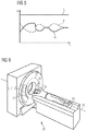
- FIG. 6 shows, by way of example and as a rough schematic diagram, an inventive medical imaging system 20 , here as a concrete example of a computed tomography device 20 .
- the computed tomography device 20 comprises a patient table 25 for supporting a patient 24 as examination object.
- the patient table 25 is displaceable along a system axis 26 into the measuring field, via which the patient 24 can be positioned in the measurement field.
- the computed tomography device 20 further comprises a gantry 22 with a source radiation detector arrangement 23 , 1 , 1 ′, 1 ′′ arranged rotatably about the system axis 26 .
- the source radiation detector arrangement 23 , 1 , 1 ′, 1 ′′ has an X-ray radiation source 23 and a radiation detector 1 , 1 ′, 1 ′′, which are aligned opposite one another so that, in operation, outgoing X-ray radiation from the focus of the X-ray radiation source 23 strikes the radiation detector 1 , 1 ′, 1 ′′.
- the radiation detector 1 , 1 ′, 1 ′′ is structured for spatially-resolved detection of the X-ray radiation into individual pixels 21 , which are arranged into a number of radiation detector rows. For each projection the radiation detector 1 , 1 ′, 1 ′′ creates a set of projection data. This projection data is subsequently further processed and computed to form a resulting image.
- Such a computed tomography device 20 is used for 3D image reconstruction.
- projection data is detected from a plurality of different projection directions.
- spiral scanning during a rotation of the source radiation detector arrangement 23 , 1 , 1 ′, 1 ′′ for example, there is a continuous displacement of the patient table 25 in the direction of the system axis 26 .
- the X-ray radiation source 23 and the radiation detector 1 , 1 ′, 1 ′′ thus move on a helical path about the patient 24 .
- the exact structure and the actual way in which such a CT operates are known to the person skilled in the art and will therefore not be explained in detail here.
Landscapes
- Physics & Mathematics (AREA)
- Spectroscopy & Molecular Physics (AREA)
- Health & Medical Sciences (AREA)
- Life Sciences & Earth Sciences (AREA)
- General Physics & Mathematics (AREA)
- High Energy & Nuclear Physics (AREA)
- Molecular Biology (AREA)
- Apparatus For Radiation Diagnosis (AREA)
- Measurement Of Radiation (AREA)
Abstract
Description
-
- a heating element, arranged between a detection layer including a plurality of detection elements and a plurality of readout units, and
- a control device, to control the heating apparatus and to regulate a heating power, introduceable into the radiation detector to heat the radiation detector.
Claims (15)
Priority Applications (1)
| Application Number | Priority Date | Filing Date | Title |
|---|---|---|---|
| US16/774,041 US10866328B2 (en) | 2016-11-02 | 2020-01-28 | Radiation detector with an intermediate layer |
Applications Claiming Priority (3)
| Application Number | Priority Date | Filing Date | Title |
|---|---|---|---|
| DE102016221481 | 2016-11-02 | ||
| DE102016221481.0 | 2016-11-02 | ||
| DE102016221481.0A DE102016221481B4 (en) | 2016-11-02 | 2016-11-02 | Radiation detector with an intermediate layer |
Related Child Applications (1)
| Application Number | Title | Priority Date | Filing Date |
|---|---|---|---|
| US16/774,041 Continuation US10866328B2 (en) | 2016-11-02 | 2020-01-28 | Radiation detector with an intermediate layer |
Publications (2)
| Publication Number | Publication Date |
|---|---|
| US20180120447A1 US20180120447A1 (en) | 2018-05-03 |
| US10598798B2 true US10598798B2 (en) | 2020-03-24 |
Family
ID=61912112
Family Applications (2)
| Application Number | Title | Priority Date | Filing Date |
|---|---|---|---|
| US15/798,626 Active US10598798B2 (en) | 2016-11-02 | 2017-10-31 | Radiation detector with an intermediate layer |
| US16/774,041 Active US10866328B2 (en) | 2016-11-02 | 2020-01-28 | Radiation detector with an intermediate layer |
Family Applications After (1)
| Application Number | Title | Priority Date | Filing Date |
|---|---|---|---|
| US16/774,041 Active US10866328B2 (en) | 2016-11-02 | 2020-01-28 | Radiation detector with an intermediate layer |
Country Status (3)
| Country | Link |
|---|---|
| US (2) | US10598798B2 (en) |
| CN (1) | CN108020858B (en) |
| DE (1) | DE102016221481B4 (en) |
Families Citing this family (12)
| Publication number | Priority date | Publication date | Assignee | Title |
|---|---|---|---|---|
| EP3418776B1 (en) * | 2017-06-21 | 2022-01-05 | Siemens Healthcare GmbH | Radiation detector and method for operating same |
| DE102018200845B4 (en) | 2018-01-19 | 2021-05-06 | Siemens Healthcare Gmbh | Assembly process for the manufacture of an X-ray detector, X-ray detector and X-ray device |
| US11067707B2 (en) * | 2018-05-07 | 2021-07-20 | Redlen Technologies, Inc. | Four-side buttable radiation detector unit and method of making thereof |
| EP3663806B1 (en) | 2018-12-03 | 2026-02-11 | Siemens Healthineers AG | Photon detector, method for producing a photon detector and x-ray device |
| US11020072B2 (en) * | 2019-06-11 | 2021-06-01 | GE Precision Healthcare LLC | System and method for regulating temperature of imaging detector sensors |
| EP3764127B1 (en) * | 2019-07-08 | 2024-08-28 | Siemens Healthineers AG | X-ray detector and x-ray apparatus with x-ray detector |
| CN112928106B (en) * | 2019-12-05 | 2024-05-17 | 同方威视技术股份有限公司 | Detector device and array panel |
| CN116250085A (en) * | 2020-11-13 | 2023-06-09 | Ams-欧司朗有限公司 | Modular components for detecting X-ray radiation |
| WO2022122374A2 (en) | 2020-12-10 | 2022-06-16 | Ams-Osram Ag | X-ray radiation sensor device |
| DE202021103494U1 (en) * | 2021-06-30 | 2021-07-19 | Siemens Healthcare Gmbh | Radiation Detector Module and Imaging System |
| EP4300140B1 (en) * | 2022-06-30 | 2026-03-11 | Siemens Healthineers AG | Detector module for an x-ray detector with a heating layer |
| EP4419949B1 (en) * | 2022-12-30 | 2026-01-21 | Shanghai United Imaging Healthcare Co., Ltd. | Photon-counting detectors for detecting radiation rays |
Citations (21)
| Publication number | Priority date | Publication date | Assignee | Title |
|---|---|---|---|---|
| US5379336A (en) * | 1992-05-21 | 1995-01-03 | Hughes Aircraft Company | Hybridized semiconductor pixel detector arrays for use in digital radiography |
| US6452186B1 (en) * | 1999-07-23 | 2002-09-17 | Koninklijke Philips Electronics N.V. | Detector for the detection for electromagnetic radiation |
| US20040113088A1 (en) * | 2002-09-23 | 2004-06-17 | Christoph Brabec | X-ray detector including a scintillator with a photosensor coating, and a production process |
| US20050051731A1 (en) * | 2003-09-10 | 2005-03-10 | Kenji Sato | Radiation detector |
| US7339176B2 (en) * | 2004-07-14 | 2008-03-04 | Orbotech Medical Solutions Ltd. | Radiation detector head |
| US20080111083A1 (en) * | 2006-11-14 | 2008-05-15 | Masashi Kondo | Scintillator panel, production method of the same and radiation image sensor |
| US20080272320A1 (en) * | 2007-05-01 | 2008-11-06 | Fujifilm Corporation | Radiation image detector |
| US20090290680A1 (en) * | 2004-03-26 | 2009-11-26 | Nova R & D, Inc. | High resolution imaging system |
| US20110155918A1 (en) * | 2009-12-30 | 2011-06-30 | Jean-Paul Bouhnik | Systems and methods for providing a shared charge in pixelated image detectors |
| US20110211668A1 (en) * | 2008-11-10 | 2011-09-01 | Koninklijke Philips Electronics N.V. | Converter element for a radiation detector |
| US20110241031A1 (en) * | 2008-12-23 | 2011-10-06 | Osram Opto Semiconductors Gmbh | Optoelectronic projection device |
| US20110253901A1 (en) * | 2008-09-23 | 2011-10-20 | Institut De Fisica D'altes Energies | Device for detecting highly energetic photons |
| US20120133001A1 (en) | 2010-11-30 | 2012-05-31 | General Electric Company | Tileable sensor array |
| US20120211663A1 (en) | 2011-02-18 | 2012-08-23 | Samsung Electronics Co., Ltd. | X-Ray Detectors Including Diffusion Barrier Films |
| US20130083887A1 (en) * | 2011-09-30 | 2013-04-04 | General Electric Company | Detector modules and methods of manufacturing |
| US20140138785A1 (en) * | 2012-03-22 | 2014-05-22 | Sionyx, Inc. | Pixel isolation elements, devices, and associated methods |
| US20140284489A1 (en) * | 2011-11-09 | 2014-09-25 | Koninklijke Philips N.V. | Radiation-sensitive detector device with charge-rejecting segment gaps |
| US20140348290A1 (en) * | 2013-05-23 | 2014-11-27 | General Electric Company | Apparatus and Method for Low Capacitance Packaging for Direct Conversion X-Ray or Gamma Ray Detector |
| US20150060681A1 (en) * | 2012-04-30 | 2015-03-05 | Koninklijke Philips N.V. | Imaging detector with anti-aliasing filter in the readout electronics and/or photosensor |
| US20160018536A1 (en) | 2014-07-15 | 2016-01-21 | Siemens Aktiengesellschaft | Detector module for an x-ray detector |
| WO2016046014A1 (en) | 2014-09-26 | 2016-03-31 | Koninklijke Philips N.V. | Radiation detector with heating device |
Family Cites Families (6)
| Publication number | Priority date | Publication date | Assignee | Title |
|---|---|---|---|---|
| US3933432A (en) * | 1974-10-29 | 1976-01-20 | Hnu Systems Inc. | Photoionization |
| WO2004027453A1 (en) * | 2002-09-18 | 2004-04-01 | Koninklijke Philips Electronics N.V. | Radiation detector |
| JP4812760B2 (en) * | 2004-07-20 | 2011-11-09 | ビー. アイ. グループ ピーエルシー | Renewable composite plastic for automotive headliner |
| US20100282972A1 (en) | 2007-11-06 | 2010-11-11 | Koninklijke Philips Electronics N.V. | Indirect radiation detector |
| EP2988307A4 (en) * | 2013-04-15 | 2017-01-25 | Toshiba Electron Tubes & Devices Co., Ltd. | Scintillator panel and process for producing same, and radiation detector and process for producing same |
| DE102014221829B4 (en) | 2014-10-27 | 2018-02-22 | Siemens Healthcare Gmbh | Method for producing a sensor board for a detector module and detector module produced thereby |
-
2016
- 2016-11-02 DE DE102016221481.0A patent/DE102016221481B4/en active Active
-
2017
- 2017-10-31 US US15/798,626 patent/US10598798B2/en active Active
- 2017-11-02 CN CN201711066631.3A patent/CN108020858B/en active Active
-
2020
- 2020-01-28 US US16/774,041 patent/US10866328B2/en active Active
Patent Citations (22)
| Publication number | Priority date | Publication date | Assignee | Title |
|---|---|---|---|---|
| US5379336A (en) * | 1992-05-21 | 1995-01-03 | Hughes Aircraft Company | Hybridized semiconductor pixel detector arrays for use in digital radiography |
| US6452186B1 (en) * | 1999-07-23 | 2002-09-17 | Koninklijke Philips Electronics N.V. | Detector for the detection for electromagnetic radiation |
| US20040113088A1 (en) * | 2002-09-23 | 2004-06-17 | Christoph Brabec | X-ray detector including a scintillator with a photosensor coating, and a production process |
| US20050051731A1 (en) * | 2003-09-10 | 2005-03-10 | Kenji Sato | Radiation detector |
| US20090290680A1 (en) * | 2004-03-26 | 2009-11-26 | Nova R & D, Inc. | High resolution imaging system |
| US7339176B2 (en) * | 2004-07-14 | 2008-03-04 | Orbotech Medical Solutions Ltd. | Radiation detector head |
| US20080111083A1 (en) * | 2006-11-14 | 2008-05-15 | Masashi Kondo | Scintillator panel, production method of the same and radiation image sensor |
| US20080272320A1 (en) * | 2007-05-01 | 2008-11-06 | Fujifilm Corporation | Radiation image detector |
| US20110253901A1 (en) * | 2008-09-23 | 2011-10-20 | Institut De Fisica D'altes Energies | Device for detecting highly energetic photons |
| US20110211668A1 (en) * | 2008-11-10 | 2011-09-01 | Koninklijke Philips Electronics N.V. | Converter element for a radiation detector |
| US20110241031A1 (en) * | 2008-12-23 | 2011-10-06 | Osram Opto Semiconductors Gmbh | Optoelectronic projection device |
| US20110155918A1 (en) * | 2009-12-30 | 2011-06-30 | Jean-Paul Bouhnik | Systems and methods for providing a shared charge in pixelated image detectors |
| US20120133001A1 (en) | 2010-11-30 | 2012-05-31 | General Electric Company | Tileable sensor array |
| US20120211663A1 (en) | 2011-02-18 | 2012-08-23 | Samsung Electronics Co., Ltd. | X-Ray Detectors Including Diffusion Barrier Films |
| US20130083887A1 (en) * | 2011-09-30 | 2013-04-04 | General Electric Company | Detector modules and methods of manufacturing |
| US20140284489A1 (en) * | 2011-11-09 | 2014-09-25 | Koninklijke Philips N.V. | Radiation-sensitive detector device with charge-rejecting segment gaps |
| US20140138785A1 (en) * | 2012-03-22 | 2014-05-22 | Sionyx, Inc. | Pixel isolation elements, devices, and associated methods |
| US20150060681A1 (en) * | 2012-04-30 | 2015-03-05 | Koninklijke Philips N.V. | Imaging detector with anti-aliasing filter in the readout electronics and/or photosensor |
| US20140348290A1 (en) * | 2013-05-23 | 2014-11-27 | General Electric Company | Apparatus and Method for Low Capacitance Packaging for Direct Conversion X-Ray or Gamma Ray Detector |
| US20160018536A1 (en) | 2014-07-15 | 2016-01-21 | Siemens Aktiengesellschaft | Detector module for an x-ray detector |
| DE102014213738A1 (en) | 2014-07-15 | 2016-01-21 | Siemens Aktiengesellschaft | Detector module for an X-ray detector |
| WO2016046014A1 (en) | 2014-09-26 | 2016-03-31 | Koninklijke Philips N.V. | Radiation detector with heating device |
Non-Patent Citations (2)
| Title |
|---|
| Office Action for German Patent Application No. 10 2016 221 481.0 dated Nov. 12, 2018 and English translation thereof. |
| Office Action for German Patent Application No. 10 2016 221 481.0 dated Nov. 12, 2018. |
Also Published As
| Publication number | Publication date |
|---|---|
| DE102016221481A1 (en) | 2018-05-03 |
| US10866328B2 (en) | 2020-12-15 |
| CN108020858A (en) | 2018-05-11 |
| CN108020858B (en) | 2021-07-06 |
| US20180120447A1 (en) | 2018-05-03 |
| DE102016221481B4 (en) | 2021-09-16 |
| US20200158890A1 (en) | 2020-05-21 |
Similar Documents
| Publication | Publication Date | Title |
|---|---|---|
| US10866328B2 (en) | Radiation detector with an intermediate layer | |
| CN104285162B (en) | Multiple-layer horizontal computer tomography (CT) detector array with least one the glimmer sensor array layer being arranged between at least two scintillator arrays layer | |
| US20160116610A1 (en) | Method for producing a sensor board for a detector module | |
| US20210186440A1 (en) | Photon-counting x-ray detector and method for operating a photon-counting x-ray detector | |
| US9945964B2 (en) | Evaluation logic of an X-ray detector with multi-level multiplexer | |
| EP1762863A2 (en) | Radiation detection module, printed circuit board, and radiological imaging apparatus | |
| RU2647206C1 (en) | Sensor device and visualization system for detecting radiation signals | |
| US11675096B2 (en) | Photon-counting X-ray detector and method for operating a photon-counting X-ray detector | |
| US7586096B2 (en) | Interface assembly for thermally coupling a data acquisition system to a sensor array | |
| US20180088248A1 (en) | X-ray detector with thermally-conductive intermediate layer | |
| US20190011578A1 (en) | X-ray detector with intermediate unit and evaluation level | |
| US11476013B2 (en) | Anti-scatter collimator and method for producing an anti-scatter collimator | |
| Zhang et al. | A depth encoding PET detector using four‐crystals‐to‐one‐SiPM coupling and light‐sharing window method | |
| US10371833B2 (en) | X-ray detector having a light source on the carrier element | |
| US20160131771A1 (en) | Optimized signal detection by quantum-counting detectors | |
| US11076822B2 (en) | Photon detector, method for producing a photon detector, and x-ray apparatus | |
| US10588583B2 (en) | X-ray detector with an arrangement of a pixelated second electrode and a scattered radiation grid | |
| US20170269236A1 (en) | Detector apparatus with detachable evaluation unit | |
| US20200158894A1 (en) | X-ray detector having a stack arrangement | |
| US20240004091A1 (en) | Detector module for an x-ray detector having a heating layer | |
| US11226422B2 (en) | X-ray detector and x-ray device with x-ray detector | |
| US20250241605A1 (en) | X-ray detector, x-ray device and method for temperature regulation | |
| US20170242135A1 (en) | Xray detector with illumination layer on converter element | |
| US10330800B2 (en) | X-ray detector with a voltage source device for generating a pulsed potential difference | |
| US10761221B2 (en) | X-ray detector comprising a converter element with rewiring unit |
Legal Events
| Date | Code | Title | Description |
|---|---|---|---|
| FEPP | Fee payment procedure |
Free format text: ENTITY STATUS SET TO UNDISCOUNTED (ORIGINAL EVENT CODE: BIG.); ENTITY STATUS OF PATENT OWNER: LARGE ENTITY |
|
| AS | Assignment |
Owner name: SIEMENS HEALTHCARE GMBH, GERMANY Free format text: ASSIGNMENT OF ASSIGNORS INTEREST;ASSIGNORS:ERGLER, THORSTEN;GEYER, HARALD;HOSEMANN, MICHAEL;AND OTHERS;SIGNING DATES FROM 20171215 TO 20171221;REEL/FRAME:044557/0742 |
|
| STPP | Information on status: patent application and granting procedure in general |
Free format text: RESPONSE AFTER FINAL ACTION FORWARDED TO EXAMINER |
|
| STPP | Information on status: patent application and granting procedure in general |
Free format text: ADVISORY ACTION MAILED |
|
| STPP | Information on status: patent application and granting procedure in general |
Free format text: DOCKETED NEW CASE - READY FOR EXAMINATION |
|
| STPP | Information on status: patent application and granting procedure in general |
Free format text: NON FINAL ACTION MAILED |
|
| STPP | Information on status: patent application and granting procedure in general |
Free format text: RESPONSE TO NON-FINAL OFFICE ACTION ENTERED AND FORWARDED TO EXAMINER |
|
| STPP | Information on status: patent application and granting procedure in general |
Free format text: NOTICE OF ALLOWANCE MAILED -- APPLICATION RECEIVED IN OFFICE OF PUBLICATIONS |
|
| STPP | Information on status: patent application and granting procedure in general |
Free format text: PUBLICATIONS -- ISSUE FEE PAYMENT VERIFIED |
|
| STCF | Information on status: patent grant |
Free format text: PATENTED CASE |
|
| MAFP | Maintenance fee payment |
Free format text: PAYMENT OF MAINTENANCE FEE, 4TH YEAR, LARGE ENTITY (ORIGINAL EVENT CODE: M1551); ENTITY STATUS OF PATENT OWNER: LARGE ENTITY Year of fee payment: 4 |
|
| AS | Assignment |
Owner name: SIEMENS HEALTHINEERS AG, GERMANY Free format text: ASSIGNMENT OF ASSIGNORS INTEREST;ASSIGNOR:SIEMENS HEALTHCARE GMBH;REEL/FRAME:066267/0346 Effective date: 20231219 |