US10592036B2 - Touch display panel and method for driving the same, and display device - Google Patents
Touch display panel and method for driving the same, and display device Download PDFInfo
- Publication number
- US10592036B2 US10592036B2 US15/938,405 US201815938405A US10592036B2 US 10592036 B2 US10592036 B2 US 10592036B2 US 201815938405 A US201815938405 A US 201815938405A US 10592036 B2 US10592036 B2 US 10592036B2
- Authority
- US
- United States
- Prior art keywords
- touch
- display panel
- intensity
- touch display
- liquid crystal
- Prior art date
- Legal status (The legal status is an assumption and is not a legal conclusion. Google has not performed a legal analysis and makes no representation as to the accuracy of the status listed.)
- Expired - Fee Related
Links
Images


Classifications
-
- G—PHYSICS
- G06—COMPUTING OR CALCULATING; COUNTING
- G06F—ELECTRIC DIGITAL DATA PROCESSING
- G06F3/00—Input arrangements for transferring data to be processed into a form capable of being handled by the computer; Output arrangements for transferring data from processing unit to output unit, e.g. interface arrangements
- G06F3/01—Input arrangements or combined input and output arrangements for interaction between user and computer
- G06F3/03—Arrangements for converting the position or the displacement of a member into a coded form
- G06F3/041—Digitisers, e.g. for touch screens or touch pads, characterised by the transducing means
- G06F3/0414—Digitisers, e.g. for touch screens or touch pads, characterised by the transducing means using force sensing means to determine a position
-
- G—PHYSICS
- G06—COMPUTING OR CALCULATING; COUNTING
- G06F—ELECTRIC DIGITAL DATA PROCESSING
- G06F3/00—Input arrangements for transferring data to be processed into a form capable of being handled by the computer; Output arrangements for transferring data from processing unit to output unit, e.g. interface arrangements
- G06F3/01—Input arrangements or combined input and output arrangements for interaction between user and computer
- G06F3/03—Arrangements for converting the position or the displacement of a member into a coded form
- G06F3/0304—Detection arrangements using opto-electronic means
-
- G—PHYSICS
- G06—COMPUTING OR CALCULATING; COUNTING
- G06F—ELECTRIC DIGITAL DATA PROCESSING
- G06F3/00—Input arrangements for transferring data to be processed into a form capable of being handled by the computer; Output arrangements for transferring data from processing unit to output unit, e.g. interface arrangements
- G06F3/01—Input arrangements or combined input and output arrangements for interaction between user and computer
- G06F3/03—Arrangements for converting the position or the displacement of a member into a coded form
- G06F3/041—Digitisers, e.g. for touch screens or touch pads, characterised by the transducing means
- G06F3/0412—Digitisers structurally integrated in a display
-
- G—PHYSICS
- G06—COMPUTING OR CALCULATING; COUNTING
- G06F—ELECTRIC DIGITAL DATA PROCESSING
- G06F3/00—Input arrangements for transferring data to be processed into a form capable of being handled by the computer; Output arrangements for transferring data from processing unit to output unit, e.g. interface arrangements
- G06F3/01—Input arrangements or combined input and output arrangements for interaction between user and computer
- G06F3/03—Arrangements for converting the position or the displacement of a member into a coded form
- G06F3/041—Digitisers, e.g. for touch screens or touch pads, characterised by the transducing means
- G06F3/042—Digitisers, e.g. for touch screens or touch pads, characterised by the transducing means by opto-electronic means
Definitions
- Embodiments of the present disclosure pertain to the technical field of touch control, and especially to a touch display panel and relevant display device, as well as corresponding method for driving the relevant display device.
- Touch screens may be divided into several categories, such as pressure sensing touch screen, resistive touch screen, capacitive touch screen, infrared touch screen and surface acoustic touch screen, and the like.
- the capacitive touch screen is undoubtedly the most widely used touch screen, comprising transverse and longitudinal electrode arrays which are formed by ITO (indium tin oxide) material and cooperate with each other to form collectively a plurality of test points which are distributed uniformly on a surface of the screen, at intersection points where they intersect with each other.
- ITO indium tin oxide
- self-capacitance may be created among adjacent electrodes
- variation of the self-capacitance at various test points may be acquired by a self-capacitance scanning, so as to implement a detection of a single touch.
- variation of the mutual-capacitance at various test points may also be acquired by mutual-capacitance scanning, so as to implement a detection of a multi-touch.
- a so-called “3D touch” is a stereoscopic touch technology which may enhance perception of both touch strength and touch area as compared with a multi-touch operation in a planar two-dimensional space.
- the 3D touch technology may only distinguish between two touch forms of “gentle/soft pressing” and “hard pressing” which differ from each other in degrees of strength of the applied pressure by touch operations, and thus has some difficulty in application thereof for detection of values of the pressure applied by touch operations and determination of touch position at which the touch operation is implemented, resulting in a difficulty in fine rating of the pressure applied by touch operations.
- a touch display panel including: a liquid crystal layer; and a detection layer for light-intensity, which is located at a light exiting side of the liquid crystal layer and is configured to detect an intensity of light passing through the liquid crystal layer at a region thereof corresponding to a touch position on the touch display panel, in both conditions that the touch position on the touch display panel is touched and not touched by a touch action.
- the touch display panel further includes an analytical unit which is arranged to be connected electrically with the detection layer for light-intensity through an electrical connector, and is configured to receive an electrical signal which is generated from the detection layer for light-intensity through the electrical connector so as to determine a magnitude of a pressure applied by the touch action and in turn to rate a level of the pressure depending on the magnitude thereof as determined.
- an analytical unit which is arranged to be connected electrically with the detection layer for light-intensity through an electrical connector, and is configured to receive an electrical signal which is generated from the detection layer for light-intensity through the electrical connector so as to determine a magnitude of a pressure applied by the touch action and in turn to rate a level of the pressure depending on the magnitude thereof as determined.
- the touch display panel further includes sealant which functions as the electrical connector and is doped with metallic material, the analytical unit being connected electrically with the detection layer for light-intensity via the metallic material inside the sealant.
- the detection layer for light-intensity includes a plurality of detectors which are arranged in an array.
- each of the plurality of detectors is one of a photoelectric detector and a thermal detector.
- the touch display panel further includes a black matrix and a signal wiring which is arranged to be connected with the plurality of detectors, orthographic projections of the plurality of detectors and the signal wiring on the liquid crystal layer being located within a orthographic projection of the black matrix on the liquid crystal layer.
- the touch display panel further includes a color filter layer which is located at a side of the detection layer for light-intensity facing away from the liquid crystal layer.
- the touch display panel further includes an array layer provided at a side of the liquid crystal layer facing away from the detection layer for light-intensity and a touch-sensing signal transmission layer provided between the liquid crystal layer and the array layer.
- a display device including: a housing; the touch display panel as above; and a drive circuit for the touch display panel.
- a method for driving the touch display panel according to claim 1 including: detecting the intensity of light passing through the liquid crystal layer at the region thereof corresponding to the touch position on the touch display panel in a condition that the touch position on the touch display panel is touched by the touch action, by the detection layer for light-intensity; and determining touch information by comparing the intensity of light passing through the liquid crystal layer in the condition that the touch position on the touch display panel is touched, with an intensity of light passing through the liquid crystal layer in a condition that the touch position on the touch display panel is not touched.
- the touch information includes a magnitude of a pressure applied by the touch action and the touch position, and determining touch information including determining the magnitude of the pressure applied by the touch action at the touch position.
- the touch display panel further includes an analytical unit, which is arranged to be connected electrically with the detection layer for light-intensity through an electrical connector, and configured to receive an electrical signal which is generated from the detection layer for light-intensity through the electrical connector so as to determine magnitude of the pressure applied by the touch action and in turn to rate a level of the pressure depending on the magnitude thereof as determined; and determining the magnitude of the pressure applied by the touch action at the touch position includes:
- determining the magnitude of the pressure applied by the touch action by comparing the first electrical signal in the condition that the touch position on the touch display panel is not touched and the second electrical signal in the condition that the touch position on the touch display panel is touched.
- the analytical unit stores therein a data table which contains ratings of the pressure applied by the touch action corresponding to different magnitudes of the pressure, and the analytical unit rates the level of the pressure depending on the magnitude thereof.
- the detection layer for light-intensity includes a plurality of detectors which are arranged in an array, and each of the plurality of detectors is marked with values of coordinates thereof, respectively.
- the intensity of light passing through the liquid crystal layer in the condition that the touch position on the touch display panel is not touched is determined by one of:
- a storage device which is located outside the analytical unit stores therein a data table which contains ratings of the pressure applied by the touch action corresponding to different magnitudes of the pressure, and the analytical unit invokes the data table from the storage device and rates the level of the pressure depending on the magnitude thereof.
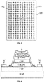
- FIG. 1 illustrates a structural schematic view of a typical exemplary embodiment of a touch display panel according to embodiments of the disclosure
- FIG. 2 illustrates a schematic view of deformation of the touch display panel as illustrated in FIG. 1 , once it is subject to a pressure applied by a touch action;
- FIG. 3 illustrates a schematic view of arrangement of a plurality of detectors within the touch display panel according to embodiments of the disclosure
- FIG. 4 illustrates a structural schematic view of a typical exemplary embodiment of a photoelectric detector within the touch display panel according to embodiments of the disclosure
- FIG. 5 illustrates a schematic flow chart of a method for driving the touch display panel according to embodiments of the disclosure
- FIG. 6 illustrates a schematic flow chart of a method for determining a magnitude of the pressure applied by the touch action according to embodiments of the disclosure.
- FIG. 7 illustrates a schematic view of a method for time-sharing driving of display signal, transferring signal (i.e., signal being delivered) and touch signal in a display control method according to an embodiment of the disclosure.
- the touch display panel 100 includes: a liquid crystal layer 20 ; and a detection layer 10 for light-intensity, which is located at a light emergent side of the liquid crystal layer 20 at which side light exits the liquid crystal layer and is configured to detect an intensity of light passing through the liquid crystal layer 20 at a region thereof corresponding to a touch position on the touch display panel, at which position the touch display panel is set to be touched.
- a light transmittance T of the touch display panel 100 may be represented as below:
- ⁇ is an azimuth angle at which the liquid crystal molecules deflect
- ⁇ n is a birefringence of the liquid crystal layer 20 .
- d is a thickness of the liquid crystal layer 20 .
- ⁇ is a wavelength of incident light.
- the touch display panel 100 may deform slightly when it is squeezed/pressed by an external acting force; in other words, the touch display panel 100 may deform slightly at a touch position thereon at which a pressure is applied by a touch action.
- a reduced thickness, and in turn a decreased amount of liquid crystal may thus be incurred there; i.e., the amount of liquid crystal molecules which may emit light there is decreased, resulting in a reduced display brightness/luminance there.
- the detection layer 10 for light-intensity may detect the intensity of light passing through the liquid crystal layer 20 at the region thereof corresponding to the touch position on the touch display panel, at which the touch display panel is set to be touched, in both conditions that the touch position on the touch display panel is touched and not touched by the touch action, and then convert two resulting optical signals into two electrical signals, respectively, each of which may for example be voltage or current. It is obvious that, the intensity of light passing through the liquid crystal layer 20 in the condition that the touch position on the touch display panel is touched, may differ from intensity of light passing through the liquid crystal layer 20 in a condition that the touch display panel is not touched, at the touch position, in turn bringing about a difference between magnitudes of the two resulting electrical signals.
- the detection layer 10 for light-intensity may then determine a variation of the intensity of light passing through the liquid crystal layer 20 at the region thereof corresponding to the touch position on the touch display panel, depending on the two intensities of light as detected above, facilitating determination of a magnitude of a pressure applied on the touch display panel by the touch action by an external detection device or an internal detection device provided within the touch display panel 100 .
- the magnitude of the pressure applied by the touch action may be determined, for example, different pressures applied during touch with different magnitudes may be preset to correspond to different display contents and display effects, then corresponding display contents and display effects may be presented on the touch display panel 100 , e.g., depending on specific magnitudes of the pressure applied by the touch action as determined above, such that display functions of the touch display panel 100 may be enriched hereby.
- the touch display panel 100 in embodiments of the disclosure may determine the magnitude of the pressure applied by the touch action by detecting the intensity of light passing through the liquid crystal layer 20 , and in turn rate the pressure applied by the touch action based on the magnitude thereof as determined, and then specify different display contents and display effects corresponding to different rating of the pressure applied by the touch action, resulting in enriched display functions.
- the touch display panel 100 further includes an analytical unit 30 , which is configured to analyze the magnitude of the pressure applied by the touch action, with a function of Force Touch or Press Touch which is implemented by rating specific level of the pressure as sensed, so as to function as the aforementioned detection device for determination of the magnitude of the pressure applied on the touch display panel, and is arranged to be connected electrically with the detection layer 10 for light-intensity through an electrical connector provided therebetween.
- the analytical unit 30 is specifically configured to receive an electrical signal which is generated from the detection layer 10 for light-intensity through the electrical connector so as to determine the magnitude of the pressure applied by the touch action.
- the analytical unit 30 is for example integrated within a touch chip, or is for example provided individually.
- FIG. 1 illustrates schematically that the analytical unit 30 is located on a first base substrate 70 .
- the analytical unit 30 is also for example chosen to be located on the second base substrate 60 .
- the analytical unit may be one selected from a group of: MCU, CPU, DSP (i.e., Digital Signal Processor), and PLC (i.e., Programmable Logic Controller) and the like, which may contain a lookup table embedded therein, or connected with a memory or storage device containing a lookup table therein, in which lookup table preset detailed ratings of various values of different magnitudes are stored and accessible by the analytical unit.
- DSP Digital Signal Processor
- PLC Programmable Logic Controller
- the detection layer 10 for light-intensity transfers the electrical signals created at the touch position in both conditions that the touch display panel is touched and not touched by the touch action, to the analytical unit 30 , respectively, and the analytical unit 30 processes both electrical signals by implementing a comparison therebetween, e.g., by calculating a difference value therebetween, such as an absolute difference, or a relative difference.
- the relative difference may for example be a percentage of the magnitude of the electrical signal in the condition that the touch position on the touch display panel is touched by the touch action versus the magnitude of the electrical signal in the condition that the touch position on the touch display panel is not touched by the touch action, or alternatively be a percentage of the absolute difference between the two electrical signals as above versus the magnitude of the electrical signal in the condition that the touch position on the touch display panel is not touched by the touch action.
- corresponding display contents and display effects may be presented on the touch display panel 100 , e.g., based on the specific pressure of a determined rating as applied by the touch action, resulting in enriched display functions.
- the touch display panel 100 for example further includes sealant 40 which is doped with metallic material 401 , such that the sealant 40 possesses relative superior electrical conductivity.
- the sealant 40 functions as aforementioned electrical connector provided between the detection layer 10 for light-intensity and the analytical unit 30 , facilitating delivery/transferring of the electrical signal to the analytical unit 30 by the detection layer 10 for light-intensity.
- the detection layer 10 for light-intensity is provided with a plurality of detectors 101 arranged in an array, each of which is configured to detect the intensity of light passing through the liquid crystal layer at a location where it is located; for example, any two adjacent detectors 101 in a same row or a same column are arranged equidistantly.
- the plurality of detectors 101 located around the portion ‘A’ may detect an intensity of light passing therethrough and convert an optical signal corresponding thereto into an electrical signal and in turn transfer such electrical signal to the analytical unit 30 ; and in another condition that the portion ‘A’ is touched, the plurality of detectors 101 may also detect an intensity of light passing therethrough and convert another optical signal corresponding thereto into another electrical signal and in turn transfer such another electrical signal to the analytical unit 30 .
- the analytical unit 30 receives both above electrical signal generated in the condition that the portion ‘A’ is not touched and above electrical signal generated in the condition that the portion ‘A’ is touched, and then determines the magnitude of the pressure applied by the touch action which acts on the portion ‘A’ by analyzing a variation between the detected intensity of light passing therethrough in the condition that the portion ‘A’ is touched and the detected intensity of light passing therethrough in the condition that the portion ‘A’ is not touched, so as to facilitate rating of the pressure applied by the touch action.
- each of the plurality of detectors 101 is one of a photoelectric detector and a thermal detector.
- FIG. 4 illustrates a structure of a relatively typical photoelectric detector, whose working principle is based on photoelectric effect.
- all semi-conductive material having appropriate energy gap or impurity ionization energy may result in the photoelectric effect; however, in order to manufacture a practical device, several factors should be taken into consideration such as performance/properties, processes, price/cost, and the like.
- a material which is available for photoelectrical detector and is useful in bands of radiation ray and visible light may be CdS, CdSe, CdTe, Si, Ge, and the like.
- each of the detectors 101 may be a CdS detector, a CdSe detector, or a CdTe detector, each type of which has a corresponding band thereof falling within both visible region and infrared region, and the field of display technology also typically utilizes visible light, i.e., above photoelectrical detectors all meet requirements in detection.
- a working principle of a thermal detector lies in that, once a semi-conductor material absorbs energy from optical radiation, its temperatures rises accordingly so as to change its electrical properties; and a most essential feature thereof differing from aforementioned photoelectrical detector lies in that it has no selectivity on light at different wavelengths.
- the touch display panel 100 further includes: a black matrix 501 which is for example arranged to be located at a side of the detection layer 10 for light-intensity facing away from both the first base substrate 70 and the liquid crystal layer 20 and to abut against a second base substrate 60 which is opposite to the first base substrate 70 , and a signal wiring 102 which is arranged to be connected with the plurality of detectors 101 , orthographic projections of the plurality of detectors 101 and the signal wiring 102 on the liquid crystal layer 20 being located within a orthographic projection of the black matrix 501 on the liquid crystal layer 20 . Therefore, any loss in aperture ratio may be avoided so as to ensure a superior display effect of the touch display panel 100 .
- the touch display panel 100 further includes a color filter layer or color film layer 50 which is located at a side of the detection layer 10 for light-intensity facing away from the liquid crystal layer 20 . And between the color filter layer 50 and the detection layer 10 for light-intensity there may for example provide additionally a first alignment layer, which is for example manufactured by PI (polyimide) material, for adjustment in orientations of liquid crystal molecules of the liquid crystal layer 20 .
- PI polyimide
- the touch display panel 100 further includes an array substrate which is provided at a side of the liquid crystal layer facing away from the detection layer 10 for light-intensity and includes: the first base substrate 70 ; an array layer 90 which is provided at a side of the liquid crystal layer 20 facing away from the detection layer 10 for light-intensity and may further be provided with thin-film transistors; and a touch-sensing signal transmission layer 80 provided between the liquid crystal layer 20 and the array layer 90 for transferring a touch signal.
- a second alignment layer which is for example manufactured by PI (polyimide) material, for adjustment in orientations of liquid crystal molecules of the liquid crystal layer 20 by itself, or by cooperation with the first alignment layer.
- a display device in embodiments of the disclosure, including a housing, the touch display panel 100 , and a drive circuit for the touch display panel. Therefore, the display device also has the advantages of the touch display panel 100 , without being repeated herein once again.
- the display device may for example be electronic paper, smartphone, tablet computer, television set, display, laptop computer, digital photo frame, navigator or any product or component having display function.
- a method for driving the touch display panel which method is applicable to the touch display panel 100 as set forth in any one technical solution as above, and includes the following steps:
- Step 1 detecting the intensity of light passing through the liquid crystal layer 20 in a condition that the touch position on the touch display panel is touched by the touch action, by the detection layer 10 for light-intensity.
- a location on the liquid crystal layer 20 corresponding to the touch position may suffer from a slight deformation, resulting in a decreased amount of liquid crystal at the position, and in turn a decrease in the intensity of light passing therethrough.
- Step 2 determining touch information, by comparing the intensity of light passing through the liquid crystal layer in the condition that the touch position on the touch display panel is touched, with an intensity of light passing through the liquid crystal layer in a condition that the touch position on the touch display panel is not touched.
- the touch information includes the touch position and the magnitude of the pressure applied by the touch action at the touch position, but not limited thereto.
- the magnitude of the pressure applied by the touch action may be determined by following steps:
- Step S 21 converting the intensity of light passing through the liquid crystal layer in the condition that the touch position on the touch display panel is not touched into a corresponding electrical signal (which is abbreviated as “first electrical signal” hereinafter for brevity) and transferring it to the analytical unit 30 ;
- Step S 22 converting the intensity of light passing through the liquid crystal layer in the condition that the touch position on the touch display panel is touched into another corresponding electrical signal (which is abbreviated as “second electrical signal” hereinafter for brevity) and transferring it to the analytical unit 30 ; and
- Step S 23 determining the magnitude of the pressure applied by the touch action, by comparing the first electrical signal in the condition that the touch position on the touch display panel is not touched and the second electrical signal in the condition that the touch position on the touch display panel is touched.
- the intensity of light passing through the liquid crystal layer in the condition that the touch position on the touch display panel is not touched is determined, e.g., by detection implemented by the detection layer 10 for light-intensity; in other words, in the condition that the touch display panel 100 is not touched, the detection layer 10 for light-intensity detects in advance the intensity of light passing through the liquid crystal layer 20 at a region thereof corresponding to a location on the touch display panel corresponding to a preset touch position.
- the intensity of light passing through the liquid crystal layer in the condition that the touch position on the touch display panel is not touched is determined, e.g., by detecting brightness of the touch display panel 100 in the condition that the touch position on the touch display panel is not touched; and typically, the brightness is positively correlated to the intensity of light passing therethrough.
- the analytical unit 30 receives both electrical signals in both conditions that the touch position on the touch display panel is touched and not touched by the touch action, it implements a comparison therebetween and a corresponding data processing, e.g., calculation of a difference therebetween, so as to determine the magnitude of the pressure applied by the touch action, and in turn rates the pressure.
- the analytical unit 30 stores therein a corresponding preset data table, in which different magnitudes of pressures applied by touch correspond to different ratings thereof, respectively; or pressures applied by touch falling in different ranges correspond to different ratings thereof, respectively.
- the rating of the pressure is also determined.
- the analytical unit 30 is associated with the preset data table which is stored in a storage device located outside the analytical unit, and the analytical unit 30 for example invokes/calls the data table from the storage device so as to rate the level of the pressure depending on the magnitude thereof, as required.
- the touch display panel 100 in the embodiments of the disclosure has more modes of touch, each of which is configured to correspond to different display contents and display effects, such that the touch display panel 100 may present corresponding display contents and display effects depending on specific mode of touch as determined, resulting in significantly enriched display functions of the touch display panel 100 .
- each of the plurality of detectors 101 is for example marked correspondingly with values of preset coordinates thereof, respectively, so as to facilitate determination of specific touch position based on the preset coordinates in a condition that variations of light intensity is detected by one or more of the plurality of detectors 101 marked with these of preset coordinates, and in turn to facilitate display of corresponding different display contents and different display effects on the touch display panel 100 depending on different touch position as determined.
- the detection layer for light-intensity is used to detect the intensity of light passing through the liquid crystal layer, and once the liquid crystal layer is subject to the pressure applied by the touch action at the touch position on the touch display panel, since the amount of liquid crystal molecules at a location corresponding to the touch position is thus decreased, then a decreased display brightness/luminance there may be incurred accordingly, resulting in a decrease in the intensity of light passing through the liquid crystal layer.
- the detection layer for light-intensity determines the variation of the intensity of light passing through the liquid crystal layer at the region thereof corresponding to the touch position on the touch display panel, depending on the two intensity of light as detected in both conditions that the touch position on the touch display panel is touched and not touched by the touch action, facilitating determination of the magnitude of a pressure applied on the touch display panel by the touch action by the external detection device or the internal detection device provided within the touch display panel.
- the detection layer for light-intensity converts the determined intensity of light into the electrical signal, and then transfers the electrical signal to the analytical unit via the electrical connector provided between the detection layer for light-intensity and the analytical unit. Since the intensity of light detected in the condition that the touch position on the touch display panel is not touched by the touch action differs from the intensity of light detected in the condition that the touch position on the touch display panel is touched by the touch action, then the electrical signal converted from the former also differs from that converted from the latter; and then analytical unit compares the two different electrical signals with each other so as to determine the magnitude of the pressure applied by the touch action there.
- different pressures applied during touch with different magnitudes may be preset to correspond to different display contents and display effects, then, for example, corresponding display contents and display effects may be presented on the touch display panel, depending on specific magnitudes of the pressure applied by the touch action as determined above, such that display functions of the touch display panel may be enriched hereby.
- the sealant is doped with metallic material, such that the sealant possesses relative superior electrical conductivity.
- the sealant functions as aforementioned electrical connector provided between the detection layer for light-intensity and the analytical unit, facilitating delivery/transferring of the electrical signal to the analytical unit via the sealant by the detection layer for light-intensity.
- the detection layer for light-intensity is provided with a plurality of detectors arranged in an array.
- the plurality of detectors and the signal wiring are arranged that orthographic projections of the plurality of detectors and the signal wiring on the liquid crystal layer are located within a orthographic projection of the black matrix on the liquid crystal layer. Therefore, any loss in aperture ratio may be avoided so as to ensure a relatively good display effect of the touch display panel.
- each of the plurality of detectors may be a CdS detector, a CdSe detector, or a CdTe detector, each type of which has corresponding band thereof falling within visible region and infrared region, and the field of display technology also typically utilizes visible light, i.e., above photoelectrical detectors all meet requirements in detection.
- the display device in embodiments of the disclosure utilizes the touch display panel, and thus possesses advantages of the touch display panel.
- the method for driving the touch display panel includes followings steps: detecting the intensity of light passing through the liquid crystal layer in the condition that the touch position on the touch display panel is touched by the touch action, by the detection layer for light-intensity; and determining touch information, by comparing the intensity of light passing through the liquid crystal layer in the condition that the touch position on the touch display panel is touched, with an intensity of light passing through the liquid crystal layer in a condition that the touch position on the touch display panel is not touched.
- the touch information includes the touch position and the magnitude of the pressure applied by the touch action at the touch position.
- the magnitude of the pressure applied by the touch action may be determined, by comparing the electrical signal in the condition that the touch position on the touch display panel is not touched with the electrical signal in the condition that the touch position on the touch display panel is touched; and the touch position may also be determined, by acquiring a position of a detector which obtains the variation of the intensity of light by detection thereof.
- corresponding display contents and display effects may be presented on the touch display panel, e.g., based on the specific pressure of a determined rating as applied by the touch action, thereby meeting requirements on diversity of display and resulting in enriched display functions.
Landscapes
- Engineering & Computer Science (AREA)
- General Engineering & Computer Science (AREA)
- Theoretical Computer Science (AREA)
- Human Computer Interaction (AREA)
- Physics & Mathematics (AREA)
- General Physics & Mathematics (AREA)
- Position Input By Displaying (AREA)
- Liquid Crystal (AREA)
Abstract
Description
Claims (14)
Applications Claiming Priority (3)
| Application Number | Priority Date | Filing Date | Title |
|---|---|---|---|
| CN201711020957 | 2017-10-27 | ||
| CN201711020957.2A CN107608563B (en) | 2017-10-27 | 2017-10-27 | Touch display panel, driving method thereof, and display device |
| CN201711020957.2 | 2017-10-27 |
Publications (2)
| Publication Number | Publication Date |
|---|---|
| US20190129519A1 US20190129519A1 (en) | 2019-05-02 |
| US10592036B2 true US10592036B2 (en) | 2020-03-17 |
Family
ID=61080059
Family Applications (1)
| Application Number | Title | Priority Date | Filing Date |
|---|---|---|---|
| US15/938,405 Expired - Fee Related US10592036B2 (en) | 2017-10-27 | 2018-03-28 | Touch display panel and method for driving the same, and display device |
Country Status (2)
| Country | Link |
|---|---|
| US (1) | US10592036B2 (en) |
| CN (1) | CN107608563B (en) |
Families Citing this family (3)
| Publication number | Priority date | Publication date | Assignee | Title |
|---|---|---|---|---|
| CN109814749B (en) * | 2018-12-18 | 2022-04-15 | 维沃移动通信有限公司 | Pressure detection device, screen assembly and mobile terminal |
| KR20210022278A (en) | 2019-08-20 | 2021-03-03 | 삼성전자주식회사 | Apparatus and Method for detecting Defective Parts with Infrared Camera |
| CN116819837B (en) * | 2023-08-25 | 2024-01-26 | 惠科股份有限公司 | Display panel, preparation method thereof and display device |
Citations (10)
| Publication number | Priority date | Publication date | Assignee | Title |
|---|---|---|---|---|
| TW200811803A (en) | 2006-08-31 | 2008-03-01 | Au Optronics Corp | Liquid crystal display with a liquid crystal touch panel having photosensors |
| US20110310049A1 (en) * | 2009-03-09 | 2011-12-22 | Fuminori Homma | Information processing device, information processing method, and information processing program |
| US20120062817A1 (en) * | 2009-05-26 | 2012-03-15 | Sharp Kabushiki Kaisha | Liquid crystal display device |
| CN103336635A (en) | 2013-05-13 | 2013-10-02 | 京东方科技集团股份有限公司 | Capacitive in-cell touch panel and display device |
| CN104880842A (en) | 2015-06-16 | 2015-09-02 | 京东方科技集团股份有限公司 | Touch display panel and display device |
| US20160065838A1 (en) * | 2014-09-02 | 2016-03-03 | Chiun Mai Communication Systems, Inc. | Device and method for using pressure-sensing touch screen to take picture |
| CN205139869U (en) | 2015-04-13 | 2016-04-06 | 希迪普公司 | Pressure detection module reaches smart mobile phone including this pressure detection module |
| US20160334898A1 (en) * | 2015-05-15 | 2016-11-17 | Intel Corporation | Micro louvers for active privacy screen |
| CN106406617A (en) | 2016-09-26 | 2017-02-15 | 京东方科技集团股份有限公司 | A touch control panel, a touch control detection method thereof and a display device |
| CN106502455A (en) | 2016-10-21 | 2017-03-15 | 厦门天马微电子有限公司 | A kind of display floater and display device |
Family Cites Families (4)
| Publication number | Priority date | Publication date | Assignee | Title |
|---|---|---|---|---|
| CN101923256B (en) * | 2010-07-30 | 2012-01-18 | 南京中电熊猫液晶显示科技有限公司 | Method for manufacturing liquid crystal display |
| CN105786255B (en) * | 2016-03-03 | 2018-11-06 | 京东方科技集团股份有限公司 | Pressure-sensing touch system and method and display system |
| CN106598338B (en) * | 2016-12-21 | 2019-09-27 | 厦门天马微电子有限公司 | A kind of display panel, driving method and display device |
| CN106896596A (en) * | 2017-03-22 | 2017-06-27 | 惠州市德赛西威汽车电子股份有限公司 | A kind of IPS panels of antiradar reflectivity |
-
2017
- 2017-10-27 CN CN201711020957.2A patent/CN107608563B/en not_active Expired - Fee Related
-
2018
- 2018-03-28 US US15/938,405 patent/US10592036B2/en not_active Expired - Fee Related
Patent Citations (16)
| Publication number | Priority date | Publication date | Assignee | Title |
|---|---|---|---|---|
| TW200811803A (en) | 2006-08-31 | 2008-03-01 | Au Optronics Corp | Liquid crystal display with a liquid crystal touch panel having photosensors |
| US8049739B2 (en) | 2006-08-31 | 2011-11-01 | Au Optronics Corp. | Liquid crystal display with a liquid crystal touch panel having photo-sensing elements |
| US20110310049A1 (en) * | 2009-03-09 | 2011-12-22 | Fuminori Homma | Information processing device, information processing method, and information processing program |
| CN102341776A (en) | 2009-03-09 | 2012-02-01 | 索尼公司 | Information processing device, information processing method, and information procession program |
| US20120062817A1 (en) * | 2009-05-26 | 2012-03-15 | Sharp Kabushiki Kaisha | Liquid crystal display device |
| US9547384B2 (en) | 2013-05-13 | 2017-01-17 | Boe Technology Group Co., Ltd. | Capacitive in-cell touch panel and display device |
| US20150185933A1 (en) * | 2013-05-13 | 2015-07-02 | Boe Technology Group Co., Ltd. | Capacitive in-cell touch panel and display device |
| CN103336635A (en) | 2013-05-13 | 2013-10-02 | 京东方科技集团股份有限公司 | Capacitive in-cell touch panel and display device |
| US20160065838A1 (en) * | 2014-09-02 | 2016-03-03 | Chiun Mai Communication Systems, Inc. | Device and method for using pressure-sensing touch screen to take picture |
| CN205139869U (en) | 2015-04-13 | 2016-04-06 | 希迪普公司 | Pressure detection module reaches smart mobile phone including this pressure detection module |
| US20160299598A1 (en) * | 2015-04-13 | 2016-10-13 | Hideep Inc. | Pressure detection module and touch input device including the same |
| US20160334898A1 (en) * | 2015-05-15 | 2016-11-17 | Intel Corporation | Micro louvers for active privacy screen |
| CN104880842A (en) | 2015-06-16 | 2015-09-02 | 京东方科技集团股份有限公司 | Touch display panel and display device |
| US10379676B2 (en) | 2015-06-16 | 2019-08-13 | Boe Technology Group Co., Ltd. | Touch display panel and display device |
| CN106406617A (en) | 2016-09-26 | 2017-02-15 | 京东方科技集团股份有限公司 | A touch control panel, a touch control detection method thereof and a display device |
| CN106502455A (en) | 2016-10-21 | 2017-03-15 | 厦门天马微电子有限公司 | A kind of display floater and display device |
Non-Patent Citations (1)
| Title |
|---|
| First Chinese Office Action dated Dec. 18, 2019, received for corresponding Chinese Application No. 201711020957.2, 25 pages. |
Also Published As
| Publication number | Publication date |
|---|---|
| CN107608563A (en) | 2018-01-19 |
| CN107608563B (en) | 2021-04-09 |
| US20190129519A1 (en) | 2019-05-02 |
Similar Documents
| Publication | Publication Date | Title |
|---|---|---|
| US10025356B2 (en) | Flexible touch screen panel and flexible display device with the same | |
| TWI594160B (en) | Display device with touch sensing and force sensing functions | |
| KR101493840B1 (en) | Liquid crystal display, display system and method for recognizing shape of object using the liquid crystal display | |
| US9547395B2 (en) | Touch and hover sensing with conductive polarizer | |
| KR100976527B1 (en) | LCD with touch screen function using photoconductor | |
| CN105528110B (en) | A kind of In-cell touch panel, display device and its driving method | |
| EP3270271B1 (en) | In-cell touch screen and display device | |
| US10592036B2 (en) | Touch display panel and method for driving the same, and display device | |
| CN105807521A (en) | Array substrate, display panel and display device | |
| EP3118727B1 (en) | In-cell touchscreen and display device | |
| JP2009151039A (en) | Display device | |
| TW201421441A (en) | Display driving circuit with photo detecting input | |
| US10191592B2 (en) | Touch-control display panel and display device, and driving method of display panel | |
| US10671224B2 (en) | Cell touch screen, method for driving the same, and display device | |
| US10222899B2 (en) | Touch substrate, touch display panel and display device | |
| TW201222352A (en) | Switchable touch display device and operating method thereof | |
| CN101840290A (en) | Reflecting type touch-control display panel and manufacturing method thereof | |
| CN104375707A (en) | Touch display panel and touch display device | |
| CN106681571A (en) | Touch screen, display device and driving method of display device | |
| CN105183253B (en) | A kind of touch-control display panel and its driving method, display device | |
| TWI413829B (en) | Reflective touch display panel and manufacturing method thereof | |
| CN107918502A (en) | Mutual capacitance type pressure sensor, touch display device and pressure sensing method thereof | |
| WO2014153880A1 (en) | Touch control display panel, touch locating method and display device | |
| US20210165261A1 (en) | Touch display panel, touch display screen and electronic device | |
| CN105824470A (en) | Touch display device and mobile terminal |
Legal Events
| Date | Code | Title | Description |
|---|---|---|---|
| AS | Assignment |
Owner name: HEFEI BOE OPTOELECTRONICS TECHNOLOGY CO., LTD., CH Free format text: ASSIGNMENT OF ASSIGNORS INTEREST;ASSIGNORS:ZHAO, YUANYANG;SHAO, XIANJIE;GU, HONGGANG;AND OTHERS;REEL/FRAME:045375/0069 Effective date: 20180208 Owner name: BOE TECHNOLOGY GROUP CO., LTD., CHINA Free format text: ASSIGNMENT OF ASSIGNORS INTEREST;ASSIGNORS:ZHAO, YUANYANG;SHAO, XIANJIE;GU, HONGGANG;AND OTHERS;REEL/FRAME:045375/0069 Effective date: 20180208 Owner name: HEFEI BOE OPTOELECTRONICS TECHNOLOGY CO., LTD., CHINA Free format text: ASSIGNMENT OF ASSIGNORS INTEREST;ASSIGNORS:ZHAO, YUANYANG;SHAO, XIANJIE;GU, HONGGANG;AND OTHERS;REEL/FRAME:045375/0069 Effective date: 20180208 |
|
| FEPP | Fee payment procedure |
Free format text: ENTITY STATUS SET TO UNDISCOUNTED (ORIGINAL EVENT CODE: BIG.); ENTITY STATUS OF PATENT OWNER: LARGE ENTITY |
|
| STPP | Information on status: patent application and granting procedure in general |
Free format text: NON FINAL ACTION MAILED |
|
| STPP | Information on status: patent application and granting procedure in general |
Free format text: RESPONSE TO NON-FINAL OFFICE ACTION ENTERED AND FORWARDED TO EXAMINER |
|
| STPP | Information on status: patent application and granting procedure in general |
Free format text: FINAL REJECTION MAILED |
|
| STPP | Information on status: patent application and granting procedure in general |
Free format text: NOTICE OF ALLOWANCE MAILED -- APPLICATION RECEIVED IN OFFICE OF PUBLICATIONS |
|
| STPP | Information on status: patent application and granting procedure in general |
Free format text: PUBLICATIONS -- ISSUE FEE PAYMENT VERIFIED |
|
| STCF | Information on status: patent grant |
Free format text: PATENTED CASE |
|
| FEPP | Fee payment procedure |
Free format text: MAINTENANCE FEE REMINDER MAILED (ORIGINAL EVENT CODE: REM.); ENTITY STATUS OF PATENT OWNER: LARGE ENTITY |
|
| LAPS | Lapse for failure to pay maintenance fees |
Free format text: PATENT EXPIRED FOR FAILURE TO PAY MAINTENANCE FEES (ORIGINAL EVENT CODE: EXP.); ENTITY STATUS OF PATENT OWNER: LARGE ENTITY |
|
| STCH | Information on status: patent discontinuation |
Free format text: PATENT EXPIRED DUE TO NONPAYMENT OF MAINTENANCE FEES UNDER 37 CFR 1.362 |
|
| FP | Lapsed due to failure to pay maintenance fee |
Effective date: 20240317 |