US10580978B2 - Current compliance layers and memory arrays comprising thereof - Google Patents
Current compliance layers and memory arrays comprising thereof Download PDFInfo
- Publication number
- US10580978B2 US10580978B2 US15/863,199 US201815863199A US10580978B2 US 10580978 B2 US10580978 B2 US 10580978B2 US 201815863199 A US201815863199 A US 201815863199A US 10580978 B2 US10580978 B2 US 10580978B2
- Authority
- US
- United States
- Prior art keywords
- ccl
- layer
- memory cell
- ald
- compositions
- Prior art date
- Legal status (The legal status is an assumption and is not a legal conclusion. Google has not performed a legal analysis and makes no representation as to the accuracy of the status listed.)
- Active
Links
- 230000015654 memory Effects 0.000 title claims abstract description 241
- 238000003491 array Methods 0.000 title abstract description 20
- 229910052714 tellurium Inorganic materials 0.000 claims abstract description 112
- 229910052732 germanium Inorganic materials 0.000 claims abstract description 93
- PORWMNRCUJJQNO-UHFFFAOYSA-N tellurium atom Chemical compound [Te] PORWMNRCUJJQNO-UHFFFAOYSA-N 0.000 claims abstract description 91
- GNPVGFCGXDBREM-UHFFFAOYSA-N germanium atom Chemical compound [Ge] GNPVGFCGXDBREM-UHFFFAOYSA-N 0.000 claims abstract description 77
- 239000000203 mixture Substances 0.000 abstract description 222
- 239000011669 selenium Substances 0.000 abstract description 136
- 238000000231 atomic layer deposition Methods 0.000 abstract description 123
- 238000000034 method Methods 0.000 abstract description 67
- 230000009477 glass transition Effects 0.000 abstract description 51
- 229910052711 selenium Inorganic materials 0.000 abstract description 38
- 229910052717 sulfur Inorganic materials 0.000 abstract description 37
- NINIDFKCEFEMDL-UHFFFAOYSA-N Sulfur Chemical compound [S] NINIDFKCEFEMDL-UHFFFAOYSA-N 0.000 abstract description 25
- 239000011593 sulfur Substances 0.000 abstract description 25
- 238000002425 crystallisation Methods 0.000 abstract description 23
- 230000008025 crystallization Effects 0.000 abstract description 23
- 229910052710 silicon Inorganic materials 0.000 abstract description 23
- BUGBHKTXTAQXES-UHFFFAOYSA-N Selenium Chemical compound [Se] BUGBHKTXTAQXES-UHFFFAOYSA-N 0.000 abstract description 19
- XUIMIQQOPSSXEZ-UHFFFAOYSA-N Silicon Chemical compound [Si] XUIMIQQOPSSXEZ-UHFFFAOYSA-N 0.000 abstract description 13
- 239000010703 silicon Substances 0.000 abstract description 11
- 239000010410 layer Substances 0.000 description 369
- 239000000463 material Substances 0.000 description 154
- 239000002243 precursor Substances 0.000 description 139
- 229910052751 metal Inorganic materials 0.000 description 83
- 239000002184 metal Substances 0.000 description 66
- 238000000151 deposition Methods 0.000 description 60
- 238000006243 chemical reaction Methods 0.000 description 59
- 229910052787 antimony Inorganic materials 0.000 description 43
- 229910044991 metal oxide Inorganic materials 0.000 description 40
- 150000004706 metal oxides Chemical class 0.000 description 40
- 238000012545 processing Methods 0.000 description 38
- WATWJIUSRGPENY-UHFFFAOYSA-N antimony atom Chemical compound [Sb] WATWJIUSRGPENY-UHFFFAOYSA-N 0.000 description 37
- 230000008021 deposition Effects 0.000 description 35
- -1 HGeCl3 Chemical compound 0.000 description 31
- DCERHCFNWRGHLK-UHFFFAOYSA-N C[Si](C)C Chemical compound C[Si](C)C DCERHCFNWRGHLK-UHFFFAOYSA-N 0.000 description 30
- 125000004429 atom Chemical group 0.000 description 30
- 150000001875 compounds Chemical class 0.000 description 30
- IJGRMHOSHXDMSA-UHFFFAOYSA-N Atomic nitrogen Chemical compound N#N IJGRMHOSHXDMSA-UHFFFAOYSA-N 0.000 description 29
- 230000008569 process Effects 0.000 description 29
- 239000012071 phase Substances 0.000 description 28
- 239000003446 ligand Substances 0.000 description 26
- 239000010408 film Substances 0.000 description 25
- 238000004519 manufacturing process Methods 0.000 description 24
- 229910005900 GeTe Inorganic materials 0.000 description 23
- 150000001787 chalcogens Chemical class 0.000 description 23
- 229910052798 chalcogen Inorganic materials 0.000 description 21
- 150000004770 chalcogenides Chemical class 0.000 description 21
- 239000007787 solid Substances 0.000 description 21
- 239000004020 conductor Substances 0.000 description 20
- 239000007789 gas Substances 0.000 description 20
- 238000007496 glass forming Methods 0.000 description 20
- 229910052799 carbon Inorganic materials 0.000 description 19
- 239000010949 copper Substances 0.000 description 19
- OKTJSMMVPCPJKN-UHFFFAOYSA-N Carbon Chemical compound [C] OKTJSMMVPCPJKN-UHFFFAOYSA-N 0.000 description 18
- 229910052757 nitrogen Inorganic materials 0.000 description 18
- 238000005229 chemical vapour deposition Methods 0.000 description 17
- 230000010354 integration Effects 0.000 description 17
- 230000004888 barrier function Effects 0.000 description 16
- 230000006399 behavior Effects 0.000 description 16
- 230000007547 defect Effects 0.000 description 16
- 229910052785 arsenic Inorganic materials 0.000 description 15
- 230000005496 eutectics Effects 0.000 description 15
- 239000000376 reactant Substances 0.000 description 14
- 229910006111 GeCl2 Inorganic materials 0.000 description 13
- QHGIKMVOLGCZIP-UHFFFAOYSA-N germanium dichloride Chemical compound Cl[Ge]Cl QHGIKMVOLGCZIP-UHFFFAOYSA-N 0.000 description 13
- 238000010438 heat treatment Methods 0.000 description 13
- 238000010587 phase diagram Methods 0.000 description 13
- 239000004065 semiconductor Substances 0.000 description 13
- 239000000758 substrate Substances 0.000 description 13
- RWSOTUBLDIXVET-UHFFFAOYSA-N Dihydrogen sulfide Chemical compound S RWSOTUBLDIXVET-UHFFFAOYSA-N 0.000 description 12
- 230000008859 change Effects 0.000 description 12
- 238000002955 isolation Methods 0.000 description 12
- 239000007788 liquid Substances 0.000 description 12
- VYPSYNLAJGMNEJ-UHFFFAOYSA-N Silicium dioxide Chemical compound O=[Si]=O VYPSYNLAJGMNEJ-UHFFFAOYSA-N 0.000 description 11
- RQNWIZPPADIBDY-UHFFFAOYSA-N arsenic atom Chemical compound [As] RQNWIZPPADIBDY-UHFFFAOYSA-N 0.000 description 11
- 230000015572 biosynthetic process Effects 0.000 description 11
- IJOOHPMOJXWVHK-UHFFFAOYSA-N chlorotrimethylsilane Chemical compound C[Si](C)(C)Cl IJOOHPMOJXWVHK-UHFFFAOYSA-N 0.000 description 11
- 229910052802 copper Inorganic materials 0.000 description 11
- 239000011521 glass Substances 0.000 description 11
- 229910000037 hydrogen sulfide Inorganic materials 0.000 description 11
- 230000036961 partial effect Effects 0.000 description 11
- 239000002244 precipitate Substances 0.000 description 11
- 239000011135 tin Substances 0.000 description 11
- 229910052721 tungsten Inorganic materials 0.000 description 11
- 229910005916 GeTe2 Inorganic materials 0.000 description 10
- 238000000137 annealing Methods 0.000 description 10
- 238000001816 cooling Methods 0.000 description 10
- NHLNJPXVJOFRNH-UHFFFAOYSA-N ethanol germanium(4+) Chemical compound [Ge+4].CCO.CCO.CCO.CCO NHLNJPXVJOFRNH-UHFFFAOYSA-N 0.000 description 10
- 230000014509 gene expression Effects 0.000 description 10
- 230000007246 mechanism Effects 0.000 description 10
- 229910052718 tin Inorganic materials 0.000 description 10
- 229910005867 GeSe2 Inorganic materials 0.000 description 9
- ATJFFYVFTNAWJD-UHFFFAOYSA-N Tin Chemical compound [Sn] ATJFFYVFTNAWJD-UHFFFAOYSA-N 0.000 description 9
- 150000004703 alkoxides Chemical group 0.000 description 9
- 239000006227 byproduct Substances 0.000 description 9
- 239000003795 chemical substances by application Substances 0.000 description 9
- 238000011049 filling Methods 0.000 description 9
- 239000002356 single layer Substances 0.000 description 9
- 239000000126 substance Substances 0.000 description 9
- 230000005641 tunneling Effects 0.000 description 9
- 229910052581 Si3N4 Inorganic materials 0.000 description 8
- 239000003638 chemical reducing agent Substances 0.000 description 8
- 238000010586 diagram Methods 0.000 description 8
- 229910021420 polycrystalline silicon Inorganic materials 0.000 description 8
- 238000010926 purge Methods 0.000 description 8
- 230000002829 reductive effect Effects 0.000 description 8
- 239000010937 tungsten Substances 0.000 description 8
- RYGMFSIKBFXOCR-UHFFFAOYSA-N Copper Chemical compound [Cu] RYGMFSIKBFXOCR-UHFFFAOYSA-N 0.000 description 7
- 238000005530 etching Methods 0.000 description 7
- 230000006870 function Effects 0.000 description 7
- 229910052740 iodine Inorganic materials 0.000 description 7
- 229920005591 polysilicon Polymers 0.000 description 7
- 239000000047 product Substances 0.000 description 7
- HQVNEWCFYHHQES-UHFFFAOYSA-N silicon nitride Chemical compound N12[Si]34N5[Si]62N3[Si]51N64 HQVNEWCFYHHQES-UHFFFAOYSA-N 0.000 description 7
- 229910052814 silicon oxide Inorganic materials 0.000 description 7
- 238000004088 simulation Methods 0.000 description 7
- 239000010936 titanium Substances 0.000 description 7
- WFKWXMTUELFFGS-UHFFFAOYSA-N tungsten Chemical compound [W] WFKWXMTUELFFGS-UHFFFAOYSA-N 0.000 description 7
- 229910006113 GeCl4 Inorganic materials 0.000 description 6
- VEXZGXHMUGYJMC-UHFFFAOYSA-N Hydrochloric acid Chemical compound Cl VEXZGXHMUGYJMC-UHFFFAOYSA-N 0.000 description 6
- 229910018110 Se—Te Inorganic materials 0.000 description 6
- QVGXLLKOCUKJST-UHFFFAOYSA-N atomic oxygen Chemical compound [O] QVGXLLKOCUKJST-UHFFFAOYSA-N 0.000 description 6
- 238000005452 bending Methods 0.000 description 6
- 229910052794 bromium Inorganic materials 0.000 description 6
- 229910052735 hafnium Inorganic materials 0.000 description 6
- 229910000449 hafnium oxide Inorganic materials 0.000 description 6
- WIHZLLGSGQNAGK-UHFFFAOYSA-N hafnium(4+);oxygen(2-) Chemical compound [O-2].[O-2].[Hf+4] WIHZLLGSGQNAGK-UHFFFAOYSA-N 0.000 description 6
- 238000002844 melting Methods 0.000 description 6
- 230000008018 melting Effects 0.000 description 6
- 229910052750 molybdenum Inorganic materials 0.000 description 6
- 229910052760 oxygen Inorganic materials 0.000 description 6
- 239000001301 oxygen Substances 0.000 description 6
- 229910052698 phosphorus Inorganic materials 0.000 description 6
- 238000001556 precipitation Methods 0.000 description 6
- 230000009257 reactivity Effects 0.000 description 6
- 125000003748 selenium group Chemical group *[Se]* 0.000 description 6
- IEXRMSFAVATTJX-UHFFFAOYSA-N tetrachlorogermane Chemical compound Cl[Ge](Cl)(Cl)Cl IEXRMSFAVATTJX-UHFFFAOYSA-N 0.000 description 6
- XLYOFNOQVPJJNP-UHFFFAOYSA-N water Substances O XLYOFNOQVPJJNP-UHFFFAOYSA-N 0.000 description 6
- 229910001868 water Inorganic materials 0.000 description 6
- GWEVSGVZZGPLCZ-UHFFFAOYSA-N Titan oxide Chemical compound O=[Ti]=O GWEVSGVZZGPLCZ-UHFFFAOYSA-N 0.000 description 5
- 125000000217 alkyl group Chemical group 0.000 description 5
- 229910052801 chlorine Inorganic materials 0.000 description 5
- 238000009826 distribution Methods 0.000 description 5
- 229910021480 group 4 element Inorganic materials 0.000 description 5
- 150000004820 halides Chemical class 0.000 description 5
- 150000002500 ions Chemical class 0.000 description 5
- PXHVJJICTQNCMI-UHFFFAOYSA-N nickel Substances [Ni] PXHVJJICTQNCMI-UHFFFAOYSA-N 0.000 description 5
- 150000004767 nitrides Chemical class 0.000 description 5
- 230000003647 oxidation Effects 0.000 description 5
- 238000007254 oxidation reaction Methods 0.000 description 5
- 238000005191 phase separation Methods 0.000 description 5
- 238000005240 physical vapour deposition Methods 0.000 description 5
- 230000001052 transient effect Effects 0.000 description 5
- 229910005866 GeSe Inorganic materials 0.000 description 4
- ZOKXTWBITQBERF-UHFFFAOYSA-N Molybdenum Chemical compound [Mo] ZOKXTWBITQBERF-UHFFFAOYSA-N 0.000 description 4
- BOTDANWDWHJENH-UHFFFAOYSA-N Tetraethyl orthosilicate Chemical compound CCO[Si](OCC)(OCC)OCC BOTDANWDWHJENH-UHFFFAOYSA-N 0.000 description 4
- NRTOMJZYCJJWKI-UHFFFAOYSA-N Titanium nitride Chemical compound [Ti]#N NRTOMJZYCJJWKI-UHFFFAOYSA-N 0.000 description 4
- MCMNRKCIXSYSNV-UHFFFAOYSA-N Zirconium dioxide Chemical compound O=[Zr]=O MCMNRKCIXSYSNV-UHFFFAOYSA-N 0.000 description 4
- 230000015556 catabolic process Effects 0.000 description 4
- 230000003247 decreasing effect Effects 0.000 description 4
- 238000009792 diffusion process Methods 0.000 description 4
- 230000005684 electric field Effects 0.000 description 4
- 230000002349 favourable effect Effects 0.000 description 4
- VBJZVLUMGGDVMO-UHFFFAOYSA-N hafnium atom Chemical group [Hf] VBJZVLUMGGDVMO-UHFFFAOYSA-N 0.000 description 4
- 229910052736 halogen Inorganic materials 0.000 description 4
- 230000001404 mediated effect Effects 0.000 description 4
- 239000011733 molybdenum Substances 0.000 description 4
- 230000002093 peripheral effect Effects 0.000 description 4
- 229910052709 silver Inorganic materials 0.000 description 4
- 125000003808 silyl group Chemical group [H][Si]([H])([H])[*] 0.000 description 4
- 229910052719 titanium Inorganic materials 0.000 description 4
- 238000003775 Density Functional Theory Methods 0.000 description 3
- 229910018105 SCl2 Inorganic materials 0.000 description 3
- 229910020343 SiS2 Inorganic materials 0.000 description 3
- BLRPTPMANUNPDV-UHFFFAOYSA-N Silane Chemical compound [SiH4] BLRPTPMANUNPDV-UHFFFAOYSA-N 0.000 description 3
- BQCADISMDOOEFD-UHFFFAOYSA-N Silver Chemical compound [Ag] BQCADISMDOOEFD-UHFFFAOYSA-N 0.000 description 3
- RTAQQCXQSZGOHL-UHFFFAOYSA-N Titanium Chemical compound [Ti] RTAQQCXQSZGOHL-UHFFFAOYSA-N 0.000 description 3
- 229910017817 a-Ge Inorganic materials 0.000 description 3
- 229910045601 alloy Inorganic materials 0.000 description 3
- 239000000956 alloy Substances 0.000 description 3
- 229910052782 aluminium Inorganic materials 0.000 description 3
- 230000008901 benefit Effects 0.000 description 3
- 239000002131 composite material Substances 0.000 description 3
- 230000007423 decrease Effects 0.000 description 3
- 238000006731 degradation reaction Methods 0.000 description 3
- 230000001419 dependent effect Effects 0.000 description 3
- 238000005137 deposition process Methods 0.000 description 3
- 238000013461 design Methods 0.000 description 3
- 239000003989 dielectric material Substances 0.000 description 3
- 239000002019 doping agent Substances 0.000 description 3
- 238000001704 evaporation Methods 0.000 description 3
- 230000008020 evaporation Effects 0.000 description 3
- VDDXNVZUVZULMR-UHFFFAOYSA-N germanium tellurium Chemical compound [Ge].[Te] VDDXNVZUVZULMR-UHFFFAOYSA-N 0.000 description 3
- 229910021476 group 6 element Inorganic materials 0.000 description 3
- 150000002367 halogens Chemical class 0.000 description 3
- 239000011261 inert gas Substances 0.000 description 3
- 229910001507 metal halide Inorganic materials 0.000 description 3
- 150000005309 metal halides Chemical class 0.000 description 3
- 125000002496 methyl group Chemical group [H]C([H])([H])* 0.000 description 3
- 229910052759 nickel Inorganic materials 0.000 description 3
- NJPPVKZQTLUDBO-UHFFFAOYSA-N novaluron Chemical compound C1=C(Cl)C(OC(F)(F)C(OC(F)(F)F)F)=CC=C1NC(=O)NC(=O)C1=C(F)C=CC=C1F NJPPVKZQTLUDBO-UHFFFAOYSA-N 0.000 description 3
- 239000007800 oxidant agent Substances 0.000 description 3
- 238000000059 patterning Methods 0.000 description 3
- 238000005325 percolation Methods 0.000 description 3
- 238000001953 recrystallisation Methods 0.000 description 3
- 230000004044 response Effects 0.000 description 3
- 230000002441 reversible effect Effects 0.000 description 3
- 229910052707 ruthenium Inorganic materials 0.000 description 3
- 229910021332 silicide Inorganic materials 0.000 description 3
- 239000004332 silver Substances 0.000 description 3
- FWMUJAIKEJWSSY-UHFFFAOYSA-N sulfur dichloride Chemical compound ClSCl FWMUJAIKEJWSSY-UHFFFAOYSA-N 0.000 description 3
- 238000007669 thermal treatment Methods 0.000 description 3
- 239000010409 thin film Substances 0.000 description 3
- 230000009466 transformation Effects 0.000 description 3
- JLTRXTDYQLMHGR-UHFFFAOYSA-N trimethylaluminium Chemical compound C[Al](C)C JLTRXTDYQLMHGR-UHFFFAOYSA-N 0.000 description 3
- ZCYVEMRRCGMTRW-UHFFFAOYSA-N 7553-56-2 Chemical compound [I] ZCYVEMRRCGMTRW-UHFFFAOYSA-N 0.000 description 2
- QGZKDVFQNNGYKY-UHFFFAOYSA-N Ammonia Chemical compound N QGZKDVFQNNGYKY-UHFFFAOYSA-N 0.000 description 2
- 101100207343 Antirrhinum majus 1e20 gene Proteins 0.000 description 2
- XKRFYHLGVUSROY-UHFFFAOYSA-N Argon Chemical compound [Ar] XKRFYHLGVUSROY-UHFFFAOYSA-N 0.000 description 2
- LFQSCWFLJHTTHZ-UHFFFAOYSA-N Ethanol Chemical compound CCO LFQSCWFLJHTTHZ-UHFFFAOYSA-N 0.000 description 2
- CPELXLSAUQHCOX-UHFFFAOYSA-N Hydrogen bromide Chemical compound Br CPELXLSAUQHCOX-UHFFFAOYSA-N 0.000 description 2
- 229910015711 MoOx Inorganic materials 0.000 description 2
- NBIIXXVUZAFLBC-UHFFFAOYSA-N Phosphoric acid Chemical compound OP(O)(O)=O NBIIXXVUZAFLBC-UHFFFAOYSA-N 0.000 description 2
- OAICVXFJPJFONN-UHFFFAOYSA-N Phosphorus Chemical compound [P] OAICVXFJPJFONN-UHFFFAOYSA-N 0.000 description 2
- 229910019897 RuOx Inorganic materials 0.000 description 2
- 229910017629 Sb2Te3 Inorganic materials 0.000 description 2
- 229910006990 Si1-xGex Inorganic materials 0.000 description 2
- 229910007020 Si1−xGex Inorganic materials 0.000 description 2
- 229910004156 TaNx Inorganic materials 0.000 description 2
- 229910010421 TiNx Inorganic materials 0.000 description 2
- 229910008764 WNx Inorganic materials 0.000 description 2
- 125000003342 alkenyl group Chemical group 0.000 description 2
- XAGFODPZIPBFFR-UHFFFAOYSA-N aluminium Chemical compound [Al] XAGFODPZIPBFFR-UHFFFAOYSA-N 0.000 description 2
- PNEYBMLMFCGWSK-UHFFFAOYSA-N aluminium oxide Inorganic materials [O-2].[O-2].[O-2].[Al+3].[Al+3] PNEYBMLMFCGWSK-UHFFFAOYSA-N 0.000 description 2
- 238000004458 analytical method Methods 0.000 description 2
- FAPDDOBMIUGHIN-UHFFFAOYSA-K antimony trichloride Chemical compound Cl[Sb](Cl)Cl FAPDDOBMIUGHIN-UHFFFAOYSA-K 0.000 description 2
- RBFQJDQYXXHULB-UHFFFAOYSA-N arsane Chemical compound [AsH3] RBFQJDQYXXHULB-UHFFFAOYSA-N 0.000 description 2
- 229910052797 bismuth Inorganic materials 0.000 description 2
- 150000001721 carbon Chemical group 0.000 description 2
- 125000004432 carbon atom Chemical group C* 0.000 description 2
- 239000012159 carrier gas Substances 0.000 description 2
- 239000002800 charge carrier Substances 0.000 description 2
- 238000003486 chemical etching Methods 0.000 description 2
- VIEXQFHKRAHTQS-UHFFFAOYSA-N chloroselanyl selenohypochlorite Chemical compound Cl[Se][Se]Cl VIEXQFHKRAHTQS-UHFFFAOYSA-N 0.000 description 2
- 229910052593 corundum Inorganic materials 0.000 description 2
- 239000002178 crystalline material Substances 0.000 description 2
- 230000001351 cycling effect Effects 0.000 description 2
- HPQAFWGDGJFSQQ-UHFFFAOYSA-N cyclohexa-2,5-dien-1-yl(trimethyl)silane Chemical compound C[Si](C)(C)C1C=CCC=C1 HPQAFWGDGJFSQQ-UHFFFAOYSA-N 0.000 description 2
- QXYJCZRRLLQGCR-UHFFFAOYSA-N dioxomolybdenum Chemical compound O=[Mo]=O QXYJCZRRLLQGCR-UHFFFAOYSA-N 0.000 description 2
- 230000009977 dual effect Effects 0.000 description 2
- 230000000694 effects Effects 0.000 description 2
- HHFAWKCIHAUFRX-UHFFFAOYSA-N ethoxide Chemical compound CC[O-] HHFAWKCIHAUFRX-UHFFFAOYSA-N 0.000 description 2
- 125000001495 ethyl group Chemical group [H]C([H])([H])C([H])([H])* 0.000 description 2
- 230000005284 excitation Effects 0.000 description 2
- CJNBYAVZURUTKZ-UHFFFAOYSA-N hafnium(IV) oxide Inorganic materials O=[Hf]=O CJNBYAVZURUTKZ-UHFFFAOYSA-N 0.000 description 2
- 125000005842 heteroatom Chemical group 0.000 description 2
- 125000004435 hydrogen atom Chemical group [H]* 0.000 description 2
- 238000010348 incorporation Methods 0.000 description 2
- 230000003993 interaction Effects 0.000 description 2
- 239000011630 iodine Substances 0.000 description 2
- 229910052741 iridium Inorganic materials 0.000 description 2
- VRIVJOXICYMTAG-IYEMJOQQSA-L iron(ii) gluconate Chemical compound [Fe+2].OC[C@@H](O)[C@@H](O)[C@H](O)[C@@H](O)C([O-])=O.OC[C@@H](O)[C@@H](O)[C@H](O)[C@@H](O)C([O-])=O VRIVJOXICYMTAG-IYEMJOQQSA-L 0.000 description 2
- 238000001459 lithography Methods 0.000 description 2
- 150000002739 metals Chemical class 0.000 description 2
- VNWKTOKETHGBQD-UHFFFAOYSA-N methane Chemical compound C VNWKTOKETHGBQD-UHFFFAOYSA-N 0.000 description 2
- BDAGIHXWWSANSR-UHFFFAOYSA-N methanoic acid Natural products OC=O BDAGIHXWWSANSR-UHFFFAOYSA-N 0.000 description 2
- 125000000956 methoxy group Chemical group [H]C([H])([H])O* 0.000 description 2
- 230000000116 mitigating effect Effects 0.000 description 2
- 230000004048 modification Effects 0.000 description 2
- 238000012986 modification Methods 0.000 description 2
- 230000006911 nucleation Effects 0.000 description 2
- 238000010899 nucleation Methods 0.000 description 2
- 125000001181 organosilyl group Chemical group [SiH3]* 0.000 description 2
- TWNQGVIAIRXVLR-UHFFFAOYSA-N oxo(oxoalumanyloxy)alumane Chemical compound O=[Al]O[Al]=O TWNQGVIAIRXVLR-UHFFFAOYSA-N 0.000 description 2
- SIWVEOZUMHYXCS-UHFFFAOYSA-N oxo(oxoyttriooxy)yttrium Chemical compound O=[Y]O[Y]=O SIWVEOZUMHYXCS-UHFFFAOYSA-N 0.000 description 2
- 239000011574 phosphorus Substances 0.000 description 2
- 238000001020 plasma etching Methods 0.000 description 2
- 230000001376 precipitating effect Effects 0.000 description 2
- WOCIAKWEIIZHES-UHFFFAOYSA-N ruthenium(iv) oxide Chemical compound O=[Ru]=O WOCIAKWEIIZHES-UHFFFAOYSA-N 0.000 description 2
- PMOBWAXBGUSOPS-UHFFFAOYSA-N selenium tetrafluoride Chemical compound F[Se](F)(F)F PMOBWAXBGUSOPS-UHFFFAOYSA-N 0.000 description 2
- 150000004756 silanes Chemical class 0.000 description 2
- 235000012239 silicon dioxide Nutrition 0.000 description 2
- 239000000377 silicon dioxide Substances 0.000 description 2
- FGEJJBGRIFKJTB-UHFFFAOYSA-N silylsulfanylsilane Chemical compound [SiH3]S[SiH3] FGEJJBGRIFKJTB-UHFFFAOYSA-N 0.000 description 2
- 238000010583 slow cooling Methods 0.000 description 2
- 150000004763 sulfides Chemical class 0.000 description 2
- 229910052715 tantalum Inorganic materials 0.000 description 2
- NNCGPRGCYAWTAF-UHFFFAOYSA-N tellurium hexafluoride Chemical compound F[Te](F)(F)(F)(F)F NNCGPRGCYAWTAF-UHFFFAOYSA-N 0.000 description 2
- 230000001988 toxicity Effects 0.000 description 2
- 231100000419 toxicity Toxicity 0.000 description 2
- JGOJQVLHSPGMOC-UHFFFAOYSA-N triethyl stiborite Chemical compound [Sb+3].CC[O-].CC[O-].CC[O-] JGOJQVLHSPGMOC-UHFFFAOYSA-N 0.000 description 2
- WGBPOPJACTZYSA-UHFFFAOYSA-N trimethyl-(4-trimethylsilylpyrazin-1-yl)silane Chemical compound C[Si](C)(C)N1C=CN([Si](C)(C)C)C=C1 WGBPOPJACTZYSA-UHFFFAOYSA-N 0.000 description 2
- 238000001039 wet etching Methods 0.000 description 2
- 229910001845 yogo sapphire Inorganic materials 0.000 description 2
- WHZBKPRMXKULAN-UHFFFAOYSA-N (triethoxy-lambda4-tellanyl)oxyethane Chemical compound CCO[Te](OCC)(OCC)OCC WHZBKPRMXKULAN-UHFFFAOYSA-N 0.000 description 1
- ABQLAMJAQZFPJI-UHFFFAOYSA-N 3-heptyloxolan-2-one Chemical compound CCCCCCCC1CCOC1=O ABQLAMJAQZFPJI-UHFFFAOYSA-N 0.000 description 1
- OSWFIVFLDKOXQC-UHFFFAOYSA-N 4-(3-methoxyphenyl)aniline Chemical compound COC1=CC=CC(C=2C=CC(N)=CC=2)=C1 OSWFIVFLDKOXQC-UHFFFAOYSA-N 0.000 description 1
- 229910016909 AlxOy Inorganic materials 0.000 description 1
- 229910017009 AsCl3 Inorganic materials 0.000 description 1
- ZOXJGFHDIHLPTG-UHFFFAOYSA-N Boron Chemical compound [B] ZOXJGFHDIHLPTG-UHFFFAOYSA-N 0.000 description 1
- KJJYLRMRFPZHTG-UHFFFAOYSA-N CCO.CCO.CCO.CCO.[SeH2] Chemical compound CCO.CCO.CCO.CCO.[SeH2] KJJYLRMRFPZHTG-UHFFFAOYSA-N 0.000 description 1
- BJOGDLXYUMJOBJ-UHFFFAOYSA-N CO.CO.CO.CO.[SeH2] Chemical compound CO.CO.CO.CO.[SeH2] BJOGDLXYUMJOBJ-UHFFFAOYSA-N 0.000 description 1
- 229910052684 Cerium Inorganic materials 0.000 description 1
- VYZAMTAEIAYCRO-UHFFFAOYSA-N Chromium Chemical compound [Cr] VYZAMTAEIAYCRO-UHFFFAOYSA-N 0.000 description 1
- 229910019044 CoSix Inorganic materials 0.000 description 1
- JPVYNHNXODAKFH-UHFFFAOYSA-N Cu2+ Chemical compound [Cu+2] JPVYNHNXODAKFH-UHFFFAOYSA-N 0.000 description 1
- 229910002531 CuTe Inorganic materials 0.000 description 1
- 229910052691 Erbium Inorganic materials 0.000 description 1
- KRHYYFGTRYWZRS-UHFFFAOYSA-N Fluorane Chemical group F KRHYYFGTRYWZRS-UHFFFAOYSA-N 0.000 description 1
- PXGOKWXKJXAPGV-UHFFFAOYSA-N Fluorine Chemical compound FF PXGOKWXKJXAPGV-UHFFFAOYSA-N 0.000 description 1
- 230000005689 Fowler Nordheim tunneling Effects 0.000 description 1
- BRDWIEOJOWJCLU-LTGWCKQJSA-N GS-441524 Chemical compound C=1C=C2C(N)=NC=NN2C=1[C@]1(C#N)O[C@H](CO)[C@@H](O)[C@H]1O BRDWIEOJOWJCLU-LTGWCKQJSA-N 0.000 description 1
- 229910052688 Gadolinium Inorganic materials 0.000 description 1
- GYHNNYVSQQEPJS-UHFFFAOYSA-N Gallium Chemical compound [Ga] GYHNNYVSQQEPJS-UHFFFAOYSA-N 0.000 description 1
- 229910005987 Ge3N4 Inorganic materials 0.000 description 1
- 229910005829 GeS Inorganic materials 0.000 description 1
- 229910005842 GeS2 Inorganic materials 0.000 description 1
- 229910003946 H3Si Inorganic materials 0.000 description 1
- UFHFLCQGNIYNRP-UHFFFAOYSA-N Hydrogen Chemical compound [H][H] UFHFLCQGNIYNRP-UHFFFAOYSA-N 0.000 description 1
- YZCKVEUIGOORGS-UHFFFAOYSA-N Hydrogen atom Chemical compound [H] YZCKVEUIGOORGS-UHFFFAOYSA-N 0.000 description 1
- 229910052765 Lutetium Inorganic materials 0.000 description 1
- 229910015617 MoNx Inorganic materials 0.000 description 1
- 229910014299 N-Si Inorganic materials 0.000 description 1
- 229910052779 Neodymium Inorganic materials 0.000 description 1
- 229910005889 NiSix Inorganic materials 0.000 description 1
- XYFCBTPGUUZFHI-UHFFFAOYSA-N Phosphine Chemical compound P XYFCBTPGUUZFHI-UHFFFAOYSA-N 0.000 description 1
- 229910052777 Praseodymium Inorganic materials 0.000 description 1
- 229910000796 S alloy Inorganic materials 0.000 description 1
- 229910018152 SeF6 Inorganic materials 0.000 description 1
- 229910008048 Si-S Inorganic materials 0.000 description 1
- 229910008045 Si-Si Inorganic materials 0.000 description 1
- 229910003828 SiH3 Inorganic materials 0.000 description 1
- 229910006336 Si—S Inorganic materials 0.000 description 1
- 229910006411 Si—Si Inorganic materials 0.000 description 1
- 229910001215 Te alloy Inorganic materials 0.000 description 1
- 229910052775 Thulium Inorganic materials 0.000 description 1
- 229910003087 TiOx Inorganic materials 0.000 description 1
- 229910008486 TiSix Inorganic materials 0.000 description 1
- WGLPBDUCMAPZCE-UHFFFAOYSA-N Trioxochromium Chemical compound O=[Cr](=O)=O WGLPBDUCMAPZCE-UHFFFAOYSA-N 0.000 description 1
- 229910052769 Ytterbium Inorganic materials 0.000 description 1
- 229910003134 ZrOx Inorganic materials 0.000 description 1
- 238000009825 accumulation Methods 0.000 description 1
- HSFWRNGVRCDJHI-UHFFFAOYSA-N alpha-acetylene Natural products C#C HSFWRNGVRCDJHI-UHFFFAOYSA-N 0.000 description 1
- 229910000147 aluminium phosphate Inorganic materials 0.000 description 1
- 229910021529 ammonia Inorganic materials 0.000 description 1
- 229910003481 amorphous carbon Inorganic materials 0.000 description 1
- 229910021417 amorphous silicon Inorganic materials 0.000 description 1
- 150000001450 anions Chemical class 0.000 description 1
- 229910052786 argon Inorganic materials 0.000 description 1
- 229910000070 arsenic hydride Inorganic materials 0.000 description 1
- OEYOHULQRFXULB-UHFFFAOYSA-N arsenic trichloride Chemical compound Cl[As](Cl)Cl OEYOHULQRFXULB-UHFFFAOYSA-N 0.000 description 1
- PNTAWGJKWLLAAW-UHFFFAOYSA-N bicyclo[4.1.0]heptane-7-carboxylic acid Chemical compound C1CCCC2C(C(=O)O)C21 PNTAWGJKWLLAAW-UHFFFAOYSA-N 0.000 description 1
- 229910002056 binary alloy Inorganic materials 0.000 description 1
- JCXGWMGPZLAOME-UHFFFAOYSA-N bismuth atom Chemical compound [Bi] JCXGWMGPZLAOME-UHFFFAOYSA-N 0.000 description 1
- 235000020304 black tie Nutrition 0.000 description 1
- 229910052796 boron Inorganic materials 0.000 description 1
- 125000000484 butyl group Chemical group [H]C([*])([H])C([H])([H])C([H])([H])C([H])([H])[H] 0.000 description 1
- 238000004364 calculation method Methods 0.000 description 1
- 239000000969 carrier Substances 0.000 description 1
- 150000001768 cations Chemical class 0.000 description 1
- ZMIGMASIKSOYAM-UHFFFAOYSA-N cerium Chemical compound [Ce][Ce][Ce][Ce][Ce][Ce][Ce][Ce][Ce][Ce][Ce][Ce][Ce][Ce][Ce][Ce][Ce][Ce][Ce][Ce][Ce][Ce][Ce][Ce][Ce][Ce][Ce][Ce][Ce][Ce][Ce][Ce][Ce][Ce][Ce][Ce][Ce][Ce] ZMIGMASIKSOYAM-UHFFFAOYSA-N 0.000 description 1
- 239000007795 chemical reaction product Substances 0.000 description 1
- 229910052804 chromium Inorganic materials 0.000 description 1
- 239000011651 chromium Substances 0.000 description 1
- 229910000423 chromium oxide Inorganic materials 0.000 description 1
- 229910052681 coesite Inorganic materials 0.000 description 1
- 230000000052 comparative effect Effects 0.000 description 1
- 230000000295 complement effect Effects 0.000 description 1
- 239000000470 constituent Substances 0.000 description 1
- 238000007796 conventional method Methods 0.000 description 1
- ZKXWKVVCCTZOLD-FDGPNNRMSA-N copper;(z)-4-hydroxypent-3-en-2-one Chemical compound [Cu].C\C(O)=C\C(C)=O.C\C(O)=C\C(C)=O ZKXWKVVCCTZOLD-FDGPNNRMSA-N 0.000 description 1
- 229910052906 cristobalite Inorganic materials 0.000 description 1
- 239000013078 crystal Substances 0.000 description 1
- 229910021419 crystalline silicon Inorganic materials 0.000 description 1
- 230000001186 cumulative effect Effects 0.000 description 1
- 125000004122 cyclic group Chemical group 0.000 description 1
- 230000000593 degrading effect Effects 0.000 description 1
- 230000002939 deleterious effect Effects 0.000 description 1
- MCQILDHFZKTBOD-UHFFFAOYSA-N diethoxy-hydroxy-imino-$l^{5}-phosphane Chemical compound CCOP(N)(=O)OCC MCQILDHFZKTBOD-UHFFFAOYSA-N 0.000 description 1
- 229910001873 dinitrogen Inorganic materials 0.000 description 1
- PXJJSXABGXMUSU-UHFFFAOYSA-N disulfur dichloride Chemical compound ClSSCl PXJJSXABGXMUSU-UHFFFAOYSA-N 0.000 description 1
- 238000007772 electroless plating Methods 0.000 description 1
- 238000009713 electroplating Methods 0.000 description 1
- UYAHIZSMUZPPFV-UHFFFAOYSA-N erbium Chemical compound [Er] UYAHIZSMUZPPFV-UHFFFAOYSA-N 0.000 description 1
- CTCOPPBXAFHGRB-UHFFFAOYSA-N ethanolate;germanium(4+) Chemical compound [Ge+4].CC[O-].CC[O-].CC[O-].CC[O-] CTCOPPBXAFHGRB-UHFFFAOYSA-N 0.000 description 1
- 125000001301 ethoxy group Chemical group [H]C([H])([H])C([H])([H])O* 0.000 description 1
- 125000002534 ethynyl group Chemical group [H]C#C* 0.000 description 1
- 229910052731 fluorine Inorganic materials 0.000 description 1
- 239000011737 fluorine Substances 0.000 description 1
- CTIKAHQFRQTTAY-UHFFFAOYSA-N fluoro(trimethyl)silane Chemical compound C[Si](C)(C)F CTIKAHQFRQTTAY-UHFFFAOYSA-N 0.000 description 1
- 235000019253 formic acid Nutrition 0.000 description 1
- UIWYJDYFSGRHKR-UHFFFAOYSA-N gadolinium atom Chemical compound [Gd] UIWYJDYFSGRHKR-UHFFFAOYSA-N 0.000 description 1
- 229910052733 gallium Inorganic materials 0.000 description 1
- 239000007792 gaseous phase Substances 0.000 description 1
- 229910021478 group 5 element Inorganic materials 0.000 description 1
- 125000005843 halogen group Chemical group 0.000 description 1
- UQEAIHBTYFGYIE-UHFFFAOYSA-N hexamethyldisiloxane Chemical compound C[Si](C)(C)O[Si](C)(C)C UQEAIHBTYFGYIE-UHFFFAOYSA-N 0.000 description 1
- 125000003707 hexyloxy group Chemical group [H]C([H])([H])C([H])([H])C([H])([H])C([H])([H])C([H])([H])C([H])([H])O* 0.000 description 1
- 229910052739 hydrogen Inorganic materials 0.000 description 1
- 239000001257 hydrogen Substances 0.000 description 1
- XMBWDFGMSWQBCA-UHFFFAOYSA-N hydrogen iodide Chemical group I XMBWDFGMSWQBCA-UHFFFAOYSA-N 0.000 description 1
- 239000012535 impurity Substances 0.000 description 1
- 238000002347 injection Methods 0.000 description 1
- 239000007924 injection Substances 0.000 description 1
- 239000011810 insulating material Substances 0.000 description 1
- 239000012212 insulator Substances 0.000 description 1
- HTXDPTMKBJXEOW-UHFFFAOYSA-N iridium(IV) oxide Inorganic materials O=[Ir]=O HTXDPTMKBJXEOW-UHFFFAOYSA-N 0.000 description 1
- 125000002510 isobutoxy group Chemical group [H]C([H])([H])C([H])(C([H])([H])[H])C([H])([H])O* 0.000 description 1
- 125000003253 isopropoxy group Chemical group [H]C([H])([H])C([H])(O*)C([H])([H])[H] 0.000 description 1
- 229910052746 lanthanum Inorganic materials 0.000 description 1
- FZLIPJUXYLNCLC-UHFFFAOYSA-N lanthanum atom Chemical compound [La] FZLIPJUXYLNCLC-UHFFFAOYSA-N 0.000 description 1
- 230000000670 limiting effect Effects 0.000 description 1
- 239000007791 liquid phase Substances 0.000 description 1
- 238000004518 low pressure chemical vapour deposition Methods 0.000 description 1
- OHSVLFRHMCKCQY-UHFFFAOYSA-N lutetium atom Chemical compound [Lu] OHSVLFRHMCKCQY-UHFFFAOYSA-N 0.000 description 1
- 239000011159 matrix material Substances 0.000 description 1
- 239000000155 melt Substances 0.000 description 1
- NBTOZLQBSIZIKS-UHFFFAOYSA-N methoxide Chemical compound [O-]C NBTOZLQBSIZIKS-UHFFFAOYSA-N 0.000 description 1
- 230000005012 migration Effects 0.000 description 1
- 238000013508 migration Methods 0.000 description 1
- 229910021421 monocrystalline silicon Inorganic materials 0.000 description 1
- ZUSRFDBQZSPBDV-UHFFFAOYSA-N n-[bis(dimethylamino)stibanyl]-n-methylmethanamine Chemical compound CN(C)[Sb](N(C)C)N(C)C ZUSRFDBQZSPBDV-UHFFFAOYSA-N 0.000 description 1
- 125000006606 n-butoxy group Chemical group 0.000 description 1
- 125000003506 n-propoxy group Chemical group [H]C([H])([H])C([H])([H])C([H])([H])O* 0.000 description 1
- QEFYFXOXNSNQGX-UHFFFAOYSA-N neodymium atom Chemical compound [Nd] QEFYFXOXNSNQGX-UHFFFAOYSA-N 0.000 description 1
- 230000007935 neutral effect Effects 0.000 description 1
- 229910000480 nickel oxide Inorganic materials 0.000 description 1
- GNRSAWUEBMWBQH-UHFFFAOYSA-N oxonickel Chemical compound [Ni]=O GNRSAWUEBMWBQH-UHFFFAOYSA-N 0.000 description 1
- BPUBBGLMJRNUCC-UHFFFAOYSA-N oxygen(2-);tantalum(5+) Chemical compound [O-2].[O-2].[O-2].[O-2].[O-2].[Ta+5].[Ta+5] BPUBBGLMJRNUCC-UHFFFAOYSA-N 0.000 description 1
- RVTZCBVAJQQJTK-UHFFFAOYSA-N oxygen(2-);zirconium(4+) Chemical compound [O-2].[O-2].[Zr+4] RVTZCBVAJQQJTK-UHFFFAOYSA-N 0.000 description 1
- 230000003071 parasitic effect Effects 0.000 description 1
- 230000037361 pathway Effects 0.000 description 1
- 125000004115 pentoxy group Chemical group [*]OC([H])([H])C([H])([H])C([H])([H])C(C([H])([H])[H])([H])[H] 0.000 description 1
- 125000001997 phenyl group Chemical group [H]C1=C([H])C([H])=C(*)C([H])=C1[H] 0.000 description 1
- IUGYQRQAERSCNH-UHFFFAOYSA-M pivalate Chemical compound CC(C)(C)C([O-])=O IUGYQRQAERSCNH-UHFFFAOYSA-M 0.000 description 1
- 238000000623 plasma-assisted chemical vapour deposition Methods 0.000 description 1
- 229910052697 platinum Inorganic materials 0.000 description 1
- 229910052696 pnictogen Inorganic materials 0.000 description 1
- 150000003063 pnictogens Chemical class 0.000 description 1
- PUDIUYLPXJFUGB-UHFFFAOYSA-N praseodymium atom Chemical compound [Pr] PUDIUYLPXJFUGB-UHFFFAOYSA-N 0.000 description 1
- 238000011112 process operation Methods 0.000 description 1
- 230000002035 prolonged effect Effects 0.000 description 1
- 125000001436 propyl group Chemical group [H]C([*])([H])C([H])([H])C([H])([H])[H] 0.000 description 1
- 238000010791 quenching Methods 0.000 description 1
- 230000000171 quenching effect Effects 0.000 description 1
- 150000003254 radicals Chemical class 0.000 description 1
- 229910052761 rare earth metal Inorganic materials 0.000 description 1
- 150000002910 rare earth metals Chemical class 0.000 description 1
- 230000008707 rearrangement Effects 0.000 description 1
- 230000008521 reorganization Effects 0.000 description 1
- 230000000717 retained effect Effects 0.000 description 1
- HYXGAEYDKFCVMU-UHFFFAOYSA-N scandium oxide Chemical compound O=[Sc]O[Sc]=O HYXGAEYDKFCVMU-UHFFFAOYSA-N 0.000 description 1
- 125000005920 sec-butoxy group Chemical group 0.000 description 1
- 229910000058 selane Inorganic materials 0.000 description 1
- LMDVZDMBPZVAIV-UHFFFAOYSA-N selenium hexafluoride Chemical compound F[Se](F)(F)(F)(F)F LMDVZDMBPZVAIV-UHFFFAOYSA-N 0.000 description 1
- 238000000926 separation method Methods 0.000 description 1
- 229910000077 silane Inorganic materials 0.000 description 1
- OLRJXMHANKMLTD-UHFFFAOYSA-N silyl Chemical compound [SiH3] OLRJXMHANKMLTD-UHFFFAOYSA-N 0.000 description 1
- 239000007790 solid phase Substances 0.000 description 1
- 229910052682 stishovite Inorganic materials 0.000 description 1
- 125000001424 substituent group Chemical group 0.000 description 1
- 230000001629 suppression Effects 0.000 description 1
- 230000002459 sustained effect Effects 0.000 description 1
- GUVRBAGPIYLISA-UHFFFAOYSA-N tantalum atom Chemical compound [Ta] GUVRBAGPIYLISA-UHFFFAOYSA-N 0.000 description 1
- MZLGASXMSKOWSE-UHFFFAOYSA-N tantalum nitride Chemical compound [Ta]#N MZLGASXMSKOWSE-UHFFFAOYSA-N 0.000 description 1
- 229910001936 tantalum oxide Inorganic materials 0.000 description 1
- PBCFLUZVCVVTBY-UHFFFAOYSA-N tantalum pentoxide Inorganic materials O=[Ta](=O)O[Ta](=O)=O PBCFLUZVCVVTBY-UHFFFAOYSA-N 0.000 description 1
- VTLHPSMQDDEFRU-UHFFFAOYSA-N tellane Chemical compound [TeH2] VTLHPSMQDDEFRU-UHFFFAOYSA-N 0.000 description 1
- 229910000059 tellane Inorganic materials 0.000 description 1
- CRMPMTUAAUPLIK-UHFFFAOYSA-N tellurium tetrafluoride Chemical compound F[Te](F)(F)F CRMPMTUAAUPLIK-UHFFFAOYSA-N 0.000 description 1
- ACOVYJCRYLWRLR-UHFFFAOYSA-N tetramethoxygermane Chemical compound CO[Ge](OC)(OC)OC ACOVYJCRYLWRLR-UHFFFAOYSA-N 0.000 description 1
- 238000005382 thermal cycling Methods 0.000 description 1
- 238000007736 thin film deposition technique Methods 0.000 description 1
- HLLICFJUWSZHRJ-UHFFFAOYSA-N tioxidazole Chemical compound CCCOC1=CC=C2N=C(NC(=O)OC)SC2=C1 HLLICFJUWSZHRJ-UHFFFAOYSA-N 0.000 description 1
- OGIDPMRJRNCKJF-UHFFFAOYSA-N titanium oxide Inorganic materials [Ti]=O OGIDPMRJRNCKJF-UHFFFAOYSA-N 0.000 description 1
- 231100000331 toxic Toxicity 0.000 description 1
- 230000002588 toxic effect Effects 0.000 description 1
- 238000000844 transformation Methods 0.000 description 1
- 229910052723 transition metal Inorganic materials 0.000 description 1
- 150000003624 transition metals Chemical class 0.000 description 1
- LXEXBJXDGVGRAR-UHFFFAOYSA-N trichloro(trichlorosilyl)silane Chemical compound Cl[Si](Cl)(Cl)[Si](Cl)(Cl)Cl LXEXBJXDGVGRAR-UHFFFAOYSA-N 0.000 description 1
- 229910052905 tridymite Inorganic materials 0.000 description 1
- KEUYHGXCOWNTEJ-UHFFFAOYSA-N trimethyl stiborite Chemical compound [Sb+3].[O-]C.[O-]C.[O-]C KEUYHGXCOWNTEJ-UHFFFAOYSA-N 0.000 description 1
- 239000013598 vector Substances 0.000 description 1
- NAWDYIZEMPQZHO-UHFFFAOYSA-N ytterbium Chemical compound [Yb] NAWDYIZEMPQZHO-UHFFFAOYSA-N 0.000 description 1
- RUDFQVOCFDJEEF-UHFFFAOYSA-N yttrium(III) oxide Inorganic materials [O-2].[O-2].[O-2].[Y+3].[Y+3] RUDFQVOCFDJEEF-UHFFFAOYSA-N 0.000 description 1
- 229910052725 zinc Inorganic materials 0.000 description 1
- 229910001928 zirconium oxide Inorganic materials 0.000 description 1
Images


Classifications
-
- H01L45/1233—
-
- G—PHYSICS
- G11—INFORMATION STORAGE
- G11C—STATIC STORES
- G11C13/00—Digital stores characterised by the use of storage elements not covered by groups G11C11/00, G11C23/00, or G11C25/00
- G11C13/0002—Digital stores characterised by the use of storage elements not covered by groups G11C11/00, G11C23/00, or G11C25/00 using resistive RAM [RRAM] elements
- G11C13/0007—Digital stores characterised by the use of storage elements not covered by groups G11C11/00, G11C23/00, or G11C25/00 using resistive RAM [RRAM] elements comprising metal oxide memory material, e.g. perovskites
-
- G—PHYSICS
- G11—INFORMATION STORAGE
- G11C—STATIC STORES
- G11C13/00—Digital stores characterised by the use of storage elements not covered by groups G11C11/00, G11C23/00, or G11C25/00
- G11C13/0002—Digital stores characterised by the use of storage elements not covered by groups G11C11/00, G11C23/00, or G11C25/00 using resistive RAM [RRAM] elements
- G11C13/0021—Auxiliary circuits
- G11C13/003—Cell access
-
- H01L27/2481—
-
- H01L45/06—
-
- H01L45/144—
-
- H01L45/1608—
-
- H—ELECTRICITY
- H10—SEMICONDUCTOR DEVICES; ELECTRIC SOLID-STATE DEVICES NOT OTHERWISE PROVIDED FOR
- H10B—ELECTRONIC MEMORY DEVICES
- H10B63/00—Resistance change memory devices, e.g. resistive RAM [ReRAM] devices
- H10B63/20—Resistance change memory devices, e.g. resistive RAM [ReRAM] devices comprising selection components having two electrodes, e.g. diodes
-
- H—ELECTRICITY
- H10—SEMICONDUCTOR DEVICES; ELECTRIC SOLID-STATE DEVICES NOT OTHERWISE PROVIDED FOR
- H10B—ELECTRONIC MEMORY DEVICES
- H10B63/00—Resistance change memory devices, e.g. resistive RAM [ReRAM] devices
- H10B63/80—Arrangements comprising multiple bistable or multi-stable switching components of the same type on a plane parallel to the substrate, e.g. cross-point arrays
- H10B63/84—Arrangements comprising multiple bistable or multi-stable switching components of the same type on a plane parallel to the substrate, e.g. cross-point arrays arranged in a direction perpendicular to the substrate, e.g. 3D cell arrays
- H10B63/845—Arrangements comprising multiple bistable or multi-stable switching components of the same type on a plane parallel to the substrate, e.g. cross-point arrays arranged in a direction perpendicular to the substrate, e.g. 3D cell arrays the switching components being connected to a common vertical conductor
-
- H—ELECTRICITY
- H10—SEMICONDUCTOR DEVICES; ELECTRIC SOLID-STATE DEVICES NOT OTHERWISE PROVIDED FOR
- H10N—ELECTRIC SOLID-STATE DEVICES NOT OTHERWISE PROVIDED FOR
- H10N70/00—Solid-state devices having no potential barriers, and specially adapted for rectifying, amplifying, oscillating or switching
- H10N70/011—Manufacture or treatment of multistable switching devices
- H10N70/021—Formation of switching materials, e.g. deposition of layers
-
- H—ELECTRICITY
- H10—SEMICONDUCTOR DEVICES; ELECTRIC SOLID-STATE DEVICES NOT OTHERWISE PROVIDED FOR
- H10N—ELECTRIC SOLID-STATE DEVICES NOT OTHERWISE PROVIDED FOR
- H10N70/00—Solid-state devices having no potential barriers, and specially adapted for rectifying, amplifying, oscillating or switching
- H10N70/20—Multistable switching devices, e.g. memristors
- H10N70/231—Multistable switching devices, e.g. memristors based on solid-state phase change, e.g. between amorphous and crystalline phases, Ovshinsky effect
-
- H—ELECTRICITY
- H10—SEMICONDUCTOR DEVICES; ELECTRIC SOLID-STATE DEVICES NOT OTHERWISE PROVIDED FOR
- H10N—ELECTRIC SOLID-STATE DEVICES NOT OTHERWISE PROVIDED FOR
- H10N70/00—Solid-state devices having no potential barriers, and specially adapted for rectifying, amplifying, oscillating or switching
- H10N70/20—Multistable switching devices, e.g. memristors
- H10N70/24—Multistable switching devices, e.g. memristors based on migration or redistribution of ionic species, e.g. anions, vacancies
- H10N70/245—Multistable switching devices, e.g. memristors based on migration or redistribution of ionic species, e.g. anions, vacancies the species being metal cations, e.g. programmable metallization cells
-
- H—ELECTRICITY
- H10—SEMICONDUCTOR DEVICES; ELECTRIC SOLID-STATE DEVICES NOT OTHERWISE PROVIDED FOR
- H10N—ELECTRIC SOLID-STATE DEVICES NOT OTHERWISE PROVIDED FOR
- H10N70/00—Solid-state devices having no potential barriers, and specially adapted for rectifying, amplifying, oscillating or switching
- H10N70/801—Constructional details of multistable switching devices
- H10N70/821—Device geometry
- H10N70/826—Device geometry adapted for essentially vertical current flow, e.g. sandwich or pillar type devices
-
- H—ELECTRICITY
- H10—SEMICONDUCTOR DEVICES; ELECTRIC SOLID-STATE DEVICES NOT OTHERWISE PROVIDED FOR
- H10N—ELECTRIC SOLID-STATE DEVICES NOT OTHERWISE PROVIDED FOR
- H10N70/00—Solid-state devices having no potential barriers, and specially adapted for rectifying, amplifying, oscillating or switching
- H10N70/801—Constructional details of multistable switching devices
- H10N70/821—Device geometry
- H10N70/828—Current flow limiting means within the switching material region, e.g. constrictions
-
- H—ELECTRICITY
- H10—SEMICONDUCTOR DEVICES; ELECTRIC SOLID-STATE DEVICES NOT OTHERWISE PROVIDED FOR
- H10N—ELECTRIC SOLID-STATE DEVICES NOT OTHERWISE PROVIDED FOR
- H10N70/00—Solid-state devices having no potential barriers, and specially adapted for rectifying, amplifying, oscillating or switching
- H10N70/801—Constructional details of multistable switching devices
- H10N70/881—Switching materials
- H10N70/882—Compounds of sulfur, selenium or tellurium, e.g. chalcogenides
- H10N70/8828—Tellurides, e.g. GeSbTe
-
- G—PHYSICS
- G11—INFORMATION STORAGE
- G11C—STATIC STORES
- G11C2213/00—Indexing scheme relating to G11C13/00 for features not covered by this group
- G11C2213/70—Resistive array aspects
- G11C2213/76—Array using an access device for each cell which being not a transistor and not a diode
Definitions
- Memory arrays are typically arranged with multiple memory cells sharing the same word lines and bit lines.
- Sneak current paths and memory cell variability in such arrays can cause various performance issues and limit the size of the array that can be achieved.
- partial or half selected cells in a given memory block may provide a sneak current path(s) around the target cell(s) and interfere with the performance of the array and limit its density as the current will scale with the number of affected partial or half selected cells.
- These sneak current paths need to be suppressed to enable low power (e.g. low current and/or low voltage) operation, reduce variabilities (e.g.
- CCL current compliance layer
- each new layer in fabricating a memory array using a stacked cross-point architecture requires additional lithography/patterning steps at critical dimensions which limits cost/bit scaling at higher densities.
- many materials used for CCLs are sensitive to temperature and exposure to high temperatures during manufacture of the memory or even during operation of the memory array could negatively impact their performance.
- many materials for CCLs may contain arsenic which has safety and manufacturing concerns.
- a CCL may comprise at least one or more of sulfur (S), selenium (Se), and tellurium (Te) as well as at least one or more of germanium (Ge) and silicon (Si).
- CCLs may be fabricated having an amorphous structure and remain amorphous when heated to 400° C. or even 450° C. and above.
- CCLs have crystallization temperatures of greater than 400° C. and, in some embodiments, glass transition temperatures of greater than 400° C.
- CCLs may be fabricated using atomic layer deposition (ALD) as a nanolaminate of layers having different compositions. The composition, number, and arrangement of the layers in the nanolaminate are selected to yield a desired composition of the CCLs.
- ALD atomic layer deposition
- a memory device comprises a CCL, the CCL comprising an interface layer and a main layer.
- the interface layer directly interfaces the main layer.
- the interface layer comprises tellurium oxide.
- the main layer comprises germanium and tellurium.
- the concentration of germanium may vary throughout the thickness of the main layer, such that the thickness extends in a direction substantially perpendicular to an interface between the main layer and the interface layer.
- the concentration of germanium in the main layer may increase toward the interface between the main layer and the interface layer.
- the concentration of germanium in the main layer may have multiple spikes throughout the thickness of the main layer.
- the concentration of tellurium in the main layer is between about 80% atomic and 99% atomic.
- the concentration of germanium in the main layer may be between about 1% atomic and 10% atomic.
- the thickness of the interface layer may be between about 0.1 nanometers and 10 nanometers. In some embodiments, the interface layer is substantially conformal. In some embodiments, the thickness of the main layer is between about 10 nanometers and 200 nanometers.
- the CCL further comprises a first electrode.
- the interface layer may be disposed between the first electrode and the main layer.
- the interface layer may directly interface the first electrode.
- the CCL further comprises a second electrode.
- the main layer may be disposed between the second electrode and the interface layer. The main layer directly may interface the second electrode.
- the memory device further comprises a memory element.
- the CCL may be stacked with and connected in series with the memory element.
- the memory element may directly interface the main layer of the CCL.
- the memory element is a resistive random-access memory (ReRAM).
- the CCL is operable as a memory cell.
- a method of forming a memory device comprising a CCL.
- the method comprises depositing an interface layer of the CCL using atomic layer deposition (ALD).
- the method also comprises depositing a main layer of the CCL using ALD.
- the interface layer directly interfaces the main layer.
- the interface layer comprises tellurium oxide.
- the main layer comprises germanium and tellurium.
- the precursors used to deposit the interface layer comprise tellurium ethoxide (Te(OC 2 H 5 ) 4 ) and water (H 2 O).
- the precursors used to deposit the main layer may comprise one or more of ((CH 3 ) 3 Si) 2 Te, Te(OEt) 4 , Ge(OEt) 4 , GeCl4, HGeCl3, and GeCl 2 .
- different ALD cycles producing layers having different compositions are used for depositing the main layer.
- the concentration of germanium may vary throughout a thickness of the main layer, the thickness extending in a direction substantially perpendicular to an interface between the main layer and the interface layer.
- FIGS. 1A-1D are schematic representations of I-V curves for a memory element comprising a CCL and a memory cell, in accordance with some embodiments.
- FIG. 2A is a schematic representation of a memory element comprising a CCL, a memory cell, and two signal lines, in accordance with some embodiments.
- FIG. 2B is a schematic illustration of a CCL being a multilayered structure, in accordance with some embodiments.
- FIGS. 2C-2E are schematic representations of a memory element comprising a CCL, in accordance with some embodiments.
- FIGS. 2F-2I are schematic representations of different profile concentrations in a CCL, in accordance with some embodiments.
- FIG. 2J is a schematic representation of a memory element comprising a CCL, a memory cell, and two signal lines, in accordance with some embodiments.
- FIGS. 2K-2N represent 3D arrays comprising multiple memory elements sharing signal lines, in accordance with some embodiments.
- FIGS. 3A and 3B are examples of I-V performance of the memory cell.
- FIG. 4A is a process flowchart of fabricating a 3D array comprising multiple memory elements sharing signal lines, in accordance with some embodiments.
- FIG. 4B is a process flowchart of fabricating a CCL in a 3D array, in accordance with some embodiments.
- FIG. 4C is an example of a nanolaminate, in accordance with some embodiments.
- FIGS. 4D and 4E are examples of concentration profiles within a CCL, in accordance with some embodiments.
- FIGS. 5A-5I-2 are schematic representations of a first example of a 3D array at different fabrication stages, in accordance with some embodiments.
- FIGS. 6A-6H-2 are schematic representations of a second example of a 3D array at different fabrication stages, in accordance with some embodiments.
- FIGS. 7A-7I-2 are schematic representations of a third example of a 3D array at different fabrication stages, in accordance with some embodiments.
- FIGS. 8A-8F illustrate examples of the stack at various stages of processing.
- FIGS. 9A-9B are schematic representations of an example of a 3D array at different fabrication stages, in accordance with some embodiments.
- FIG. 10 is a phase diagram for Ge—Te combinations with another component.
- FIGS. 11, 12, and 13A-13D are glass transition temperature (T g ) diagrams for different compositions.
- FIG. 14 is a simulation of a charge layer on one side of a semiconducting layer between two electrodes showing current-voltage non-linearity.
- FIG. 15 is an example of an I-V plot where the resulting current is determined by thermions above a barrier layer.
- FIG. 16A-B are glass transition temperature (T g ) diagrams for different compositions.
- FIGS. 17A-17C illustrates phase diagrams for different types of sulfur-containing precursors.
- FIGS. 18A and 18B illustrate merit functions for different combinations of silicon, tellurium, germanium, selenium, and sulfur or more, specifically, low-T phases in FIG. 18A and high-T phases in FIG. 18B .
- FIGS. 19A-26 illustrate plots of different glass transition temperatures, in which corners represent different compositions of pure materials, including pure binaries.
- FIG. 27 illustrates an order of film deposition in an example ALD process.
- CCLs may be used to block these sneak current paths.
- a CCL may be used in a two-terminal memory array to reduce/retard memory leakage currents, Specifically, a CCL element may be used to avoid disturbance of unselected and/or partially (e.g. half) selected memory elements and to minimize the cumulative parasitic current leakage across the entire array. It is advantageous for bipolar memory elements to have CCLs with symmetric characteristics for both forward and reverse polarities, which is not achievable with conventional diodes used as the CCL. For purposes of this disclosure, CCLs used in bipolar memory elements are referred to as bipolar CCLs or simply CCLs.
- bipolar CCLs include symmetric current characteristics at forward and reverse voltage biases, low current (current suppression) up to a threshold voltage, high current above the threshold voltage (low resistance above the threshold voltage), and large current-voltage non-linearity (NL) at the threshold voltage (e.g., an increase of 4 or more orders of magnitude in the current value per applied Volt, and in some embodiments an increase of 6 or more orders of magnitude in the current value per applied Volt).
- bipolar CCLs may exhibit asymmetry in that the magnitude of the threshold voltages may differ and/or the NL may differ for each polarity.
- CCLs are provided with a non-linear current-voltage (I-V) behavior, including low current at low voltages and high current at higher voltages.
- FIGS. 1A-1D are schematic representations of I-V curves for a memory element comprising a CCL and a memory cell, in accordance with some embodiments. Two different examples of CCLs are presented in these curves.
- Unipolar CCLs can be used together with unipolar memory cells or memory cells operated in unipolar fashion, whereas bipolar CCLs can be used with bipolar memory cells or memory cells operated in bipolar fashion.
- Example memory cell types include but are not limited to phase change memory (PCM), resistive random-access memory (ReRAM), conductive bridge random-access memory (CBRAM), electrolytic memory, and ferroelectric memory.
- PCM phase change memory
- ReRAM resistive random-access memory
- CBRAM conductive bridge random-access memory
- electrolytic memory and ferroelectric memory.
- the unipolar CCL can have high resistance at reverse polarity conditions.
- Both unipolar and bipolar CCLs can have high resistance at low voltages. These CCLs can prevent sneak-through current, even when adjacent memory elements are in low-resistance state.
- the non-linear I-V can also provide the CCL with low resistance at higher voltages so that there is no significant voltage drop across the CCL during switching.
- a CCL may be also referred to as a selector, a selector element, a current limiter, a current compliance layer, a current steering element, or a threshold switch.
- a CCL is defined as a circuit element operable to limit the current through the CCL at one set of conditions and allow for the current to pass through the CCL at another set of conditions. Some examples of the conditions include the programming voltages across the CCL.
- One challenging aspect of integrating CCLs into memory arrays, and particularly into 3D memory arrays, is to maintain their characteristics described above after fabricating these CCLs during the manufacturing process. For example, after CCLs are fabricated on a substrate (which may contain CMOS devices, access transistors, peripheral transistors, core and peripheral circuitry under and/or adjacent to the memory array) additional processing may be performed to fabricate other components. This processing may involve heating and/or exposing the previously fabricated CCLs to processing environments which may deleteriously alter their properties. Heating can be particularly challenging as CCLs may change their morphology (e.g., crystalize) while heated. Proposed aspects of mitigating crystallization of CCL materials involve using materials that remain amorphous when heated to 400° C.
- CCLs have crystallization temperatures of greater than 400° C. and, in some embodiments, CCLs have glass transition temperatures of greater than 400° C. Additionally, CCLs may temporally and spatially (locally) melt while heated and return to the amorphous state by rapid transient cooling. Furthermore, low post-CCL-deposition temperature processing and integration schemes may be used to reduce and prevent crystallization of amorphous CCLs. In some embodiments, CCLs maintain their crystallinity content to less than 40% by volume, less than 30% by volume, less than 20% by volume, less than 10% by volume, and even less than 5% by volume.
- the composition of a CCL may be selected away from the known low-T and high-T stable crystalline phases. For example, merit functions for different combinations of silicon, tellurium, germanium, selenium, and sulfur may be evaluated. Some examples of these merit functions are presented in FIGS. 18A and 18B . Specifically, FIG. 18A only illustrates low-I phases, while FIG. 18B only illustrate high-phases.
- the selected compositions may have values higher than a certain merit function threshold value.
- Topological considerations are used to determine compositions for CCLs where the material is likely to form glasses. It should be noted that even proximity to a stable crystalline stoichiometry still makes glass-to-crystalline transformation very easy. In particular, compositions that are close to crystalline stoichiometries may exhibit memory-like behavior.
- melting-temperature considerations can be used to evaluate memory-vs-selector behavior at compositions where the crystalline phase is well-defined, these melting-temperature considerations become less meaningful far away from compositions with well-defined crystalline phase. This may be due to the ambiguity of the definition of melting temperature at those compositions.
- the proximity itself to the crystalline compositions can be used as an indicator of a likelihood of a glass-to-crystalline transformation. For example, a figure of merit can be defined for a given composition x 0 by going over all known stable crystalline compounds C. Each compound may be approximated by its “ideal” stoichiometry x C .
- Phase diagrams show that crystalline chalcogenide binary compounds (that are thermodynamically stable) do not deviate significantly from one of such well-defined stoichiometries, such as GeTe or Si 2 Te 3 .
- the sum of inverse “normalized distances” n(x,x C ) in the composition space may be considered. Recognizing that both x and x C are actually multi-dimensional vectors ( ⁇ x i ⁇ and ⁇ x C i ⁇ , e.g.
- the “normalized distance” n(x,x C ) may be calculated as
- Low-T crystalline phases are identified as Ge, GeS, GeS 2 , S, Se, GeSe, GeSe 2 , Si, SiS 2 , SiSe 2 , GeTe, Si 2 Te 3 , Si 3 N 4 , Ge 3 N 4 , and S 4 N 4 .
- High-T crystalline phases may additionally include SiS and/or SiSe. CCL compositions close to these phases should be avoided for reliable manufacturing and operation of amorphous selector.
- ALD cycles that deposit three different chalcogenide materials are used. Specifically, two different binary components formed using group IV and group VI elements (e.g., GeSe and SiSe). An additional pure chalcogen (e.g., Te) may be added.
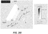
- FIGS. 19A-21I and FIGS. 22A-24I illustrate plots in which corners represent different compositions of pure materials, including pure binaries. The closer a particular CCL composition is to a given corner, the larger number of ALD cycles for this material is needed.
- the number of the ALD cycles for each of the individual materials is selected such as to obtain an average composition with high Tg, high glass-forming ability and away from the known low-T and high-T stable crystalline phase stoichiometries.
- the number of consecutive cycles depositing the same material is kept to the minimum (such as depositing less than a monolayer, or less than 3 monolayers, of given material), so as to provide best intermixing of constituent elements within an amorphous structure.
- the materials are selected such as to lie fully outside the white-color-shaded areas (limited by the dotted line) in the following plots shown in FIGS. 19A-21I , or alternatively within the lightly-shaded area as close as possible (based on other considerations) to the dashed line.
- Tg the materials with high Tg based on the following plot are selected in FIGS. 19A-19I .
- the materials in the darker areas in FIGS. 20A-20I are selected for to low-T competing compounds.
- the materials in the darker areas in FIGS. 21A-21I are selected for to high-T competing compounds.
- material compositions may be selected such that these compositions lie fully outside, the white-color-shaded areas (limited by the dotted line), or alternatively within the lightly-shaded area as close as possible (based on other considerations) to the dashed line.
- Tg the materials with high Tg based on the following plot are selected in FIGS. 22A-22I .
- the materials in the darker areas in FIGS. 23A-23I are selected for to low-T competing compounds.
- the materials in the darker areas in FIGS. 24A-24I are selected for to high-T competing compounds.
- CCLs described herein may be fabricated from different materials, such as at least one of Group VIB chalcogens.
- a CCL may also include at least one of Group IVB semiconductor elements.
- the CCL may also include an electropositive metal element (e.g., CuTe, CuS).
- Examples of Group VIB chalcogens are sulfur (S), selenium (Se), and tellurium (Te).
- Examples of Group IVB semiconductor elements are germanium (Ge), and silicon (Si).
- electropositive metal elements are transition metals, such as copper (Cu), silver (Ag), titanium (Ti), molybdenum (Mo), tungsten (W) and the like.
- the concentration of the one or more Group VIB chalcogens in the CCL may be greater than that of the one or more Group IVB semiconductor elements, e.g., equal to or greater than four times the concentration of the one or more Group IVB semiconductor elements. In some embodiments, the concentration of the one or more Group VIB chalcogens in the CCL may be greater than that of the one or more electropositive metal elements, e.g., equal to or greater than four times the concentration of the one or more electropositive metal elements.
- the concentration of the one or more Group VIB chalcogens in the CCL may be greater than the combined concentration of the one or more Group IVB semiconductor elements and the one or more electropositive metal elements, e.g., equal to or greater than four times the combined concentration of the one or more Group IVB semiconductor elements and the one or more electropositive metal elements.
- materials that can be use in CCL include aluminum (Al), gallium (Ga), carbon (C), nitrogen (N), phosphorus (P), antimony (Sb), bismuth (Bi), and/or arsenic (As). In some embodiments, it is preferable to not include materials such as arsenic (As) which poses safety and manufacturing concerns.
- a CCL may comprise at least germanium (Ge) and at least one of sulfur (S), selenium (Se), or tellurium (Te).
- the combined atomic concentration of sulfur (S), selenium (Se), and tellurium (Te) may be equal or greater than that of germanium.
- nitrogen (N) and/or carbon (C) may be added to the above composition of the CCL. Nitrogen (N) and/or carbon (C) may be added by cyclic exposure or subsequent annealing in a nitrogen (N) and/or carbon (C) containing environment. Additional examples are described below. It should be noted that subscripts presented in this disclosure typically represent percentage values whereby all subscript values for a given composition add to 100 percent. However, other notations may be used as well (e.g., Ge 0.2 Te 0.8 and GeTe 4 ).
- a CCL may be fabricated as a conformal layer or a substantially conformal (>75%) layer.
- Conformality is a measure of film thickness uniformity across a three-dimensional surface or structure.
- the thickness of the CCL layer within a three-dimensional structure such as the sidewall is at least 75% that of the field area.
- the CCL is at least 85% conformal, and in some embodiments, the CCL is at least 95% conformal.
- the thickness of the CCL may be less than or equal to 200 Angstroms, or in some embodiments, less than or equal to 100 Angstroms or, even less than or equal to 50 Angstroms.
- the CCL may be substantially amorphous (e.g., more than 50% by volume amorphous in some embodiments or more than 80% by volume amorphous in some embodiments) or even fully amorphous in some embodiments (e.g., more than 99% by volume being amorphous).
- a thin, conformal CCL aids in 3D (vertical) integration schemes of the memory arrays by conserving space and enabling true vertical integration beyond multi-layered 2D cross-point stacks to achieve 3D density. Additionally, a uniform film thickness facilitates uniform CCL properties. Conformal deposition techniques with compositional and thickness control such as ALD or suitable CVD process regime(s) with compositional and thickness control and conformal deposition is preferred.
- a thermally stable CCL prevents CCL degradation during the manufacturing process of the integrated memory device and arrays (and subsequent processing) as well as during operation.
- An amorphous CCL is preferred over one that may change between amorphous and crystalline state during manufacture and/or during operation which can cause degradation of the CCL performance or render it inoperable as a CCL.
- atomic layer deposition (ALD) or ALD-derivatives are used to fabricate the CCL.
- RTP rapid thermal processing
- UV ultraviolent
- laser photo, ion, radical, and/or atom processing.
- Chemical vapor deposition (CVD) or CVD derivatives including but not limited to flow modulated, cyclical, low pressure, plasma (direct or remote), e-beam, RTP, UV, laser, photo, ion, radical, atom assisted CVD may be used as well.
- the CCUs composition is controlled by fabricating a stack containing multiple layers whereby some layers may have differing compositions.
- the number, arrangement (in the stack), composition, and other characteristics of these layers determine the CCL's overall composition and distribution of different materials (e.g., elements) throughout the thickness of the CCL.
- the thickness of the CCL is a dimension in the direction of the deposition.
- concentrations of germanium and tellurium in the CCL may be controlled by depositing a number (m) of germanium-tellurium layers and a number (n) of tellurium layers.
- the number and position of the layers in the stack fabricating the CCL is defined by the number of ALD cycles and the order of these cycles.
- FIG. 2A is a schematic representation of memory element 200 comprising CCL 202 , memory cell 204 , first signal line 201 (e.g., a bit line), and second signal line 203 (e.g., a word line), in accordance with some embodiments.
- CCL 202 and memory cell 204 are stacked between first signal line 201 and second signal line 203 and interconnected in series.
- CCM 202 and memory cell 204 stacking can be in any orientation/order relative to each other and CCL 202 and memory cell 204 may take a number of different non-planar shapes as further described below.
- CCL 202 and memory cell 204 may directly interface as, for example, shown in FIG. 2A .
- current compliance layer (CCL) 202 is a multilayered structure as, for example, shown in FIG. 2B .
- the multilayered structure can provide various characteristics that are generally not available with single-layered structures.
- a multilayered structure has an interface between two distinct layers. Many CCL materials are amorphous and need to remain so during operation. Multilayered structures can enhance the stability of the amorphous phase by introducing additional interfaces which retard atomic rearrangements required for crystallization.
- CCL 202 may comprise interface layer 202 b and main layer 202 c , which has a different composition and/or morphology than interface layer 202 b .
- CCL 202 comprises optional first electrode 202 a and/or optional second electrode 202 d .
- CCL 202 may be a standalone component, with both first electrode 202 a and second electrode 202 d present, as shown in FIG. 2B .
- both first electrode 202 a and second electrode 202 d may still be present even if CCL 202 is integrated into memory element 200 , e.g., together with memory cell 204 , as shown in FIG. 2E .
- first electrode 202 a may be positioned between memory cell 204 and one of interface layer 202 b and main layer 202 c
- second electrode 202 d may be positioned between a signal line and the other one of interface layer 202 b and main layer 202 c
- the example shown in FIG. 2E has first electrode 202 a of CCL 202 positioned between memory cell 204 and interface layer 202 b
- Second electrode 202 d is positioned between second signal line 203 and main layer 202 c
- first electrode 202 a of CCL 202 may be used to control voltage across CCL 202 independently from controlling the voltage across memory cell 204 , and may be referred to as an intermediate electrode.
- Second electrode 202 d may be used, for example, to provide a specific interface to main layer 202 c that, for example, cannot be achieved with second signal line 203 .
- second signal line 203 may be formed from less resistive material than second electrode 202 d.
- CCL 202 may have only one of first electrode 202 a and second electrode 202 d or no electrodes at all.
- FIG. 2C illustrates an example in which interface layer 202 b directly interfaces memory cell 204 , while main layer 202 c directly interfaces second signal line 203 .
- interface layer 202 b may directly interface a signal line, while main layer 202 c may directly interface memory cell 204 .
- FIG. 2B illustrates another example in which first electrode 202 a is disposed between interface layer 202 b and memory cell 204 , while main layer 202 c directly interfaces second signal line 203 .
- first electrode 202 a may be disposed between main layer 202 c and memory cell 204 , while interface layer 202 b may directly interface a signal line.
- a 1R1S device comprises a lower electrode (which may be a compound electrode, e.g., tungsten/carbon bilayer), followed CCL 202 , followed by an intermediate electrode. The voltage of this intermediate electrode may not externally controlled.
- the intermediate electrode may be used as a diffusion/thermal barrier.
- the 1R1S may also comprise a memory element, disposed over the intermediate electrode, and an upper electrode disposed over the memory element.
- CCL 202 may be also operable as a memory cell.
- the dual function of CCL 202 may be attributed, for example, to an interface presented in the multilayered design and, in some embodiments, to a concentration gradient of various components in one or both layers of CCL 202 as further described below.
- the resistance of the CCL layer may be modulated by changes in the concentration gradient of one or more CCL elementary components. This gradient can be altered by appropriate application of electric fields which will drive motion of the elements toward or away from the applied electric field.
- Interface layer 202 b may comprise tellurium oxide.
- Tellurium oxide is used to enhance the growth of subsequent CCL materials.
- Tellurium oxide can be formed using ALD providing a relatively high reactive surface for subsequent CCL deposition.
- Tellurium oxide is chemically compatible with typical CCL materials and has high thermal stability.
- the thickness of interface layer 202 b may be between about 0.1 nanometers and 10 nanometers or, more specifically, between about 1 nanometer and 5 nanometers. Interface layer 202 b needs to be sufficiently thick such that first electrode 202 a or any other component, which main layer 202 c is formed over, is physically isolated from main layer 202 c . Furthermore, at low thickness values, interface layer 202 b may not be sufficiently conformal or even coat the entire surface supporting interface 202 b.
- Interface layer 202 b separates main layer 202 c from first electrode 202 a and, in some embodiments, helps with nucleation of main layer 202 c .
- interface layer 202 b is formed prior to main layer 202 c .
- Main layer 202 c is then deposited directly over interface layer 202 b .
- interface layer 202 b provides a more uniform surface with a sufficient number of nucleation sites to achieve a continuous main layer for very thin films with low roughness.
- Main layer 202 c may comprise a combination of germanium, selenium, silicon, arsenic, antimony, tellurium, nitrogen, tin, and sulfur or, more specifically, a combination of tellurium and germanium.
- the concentration of tellurium in main layer 202 c may be between about 80% atomic and 99% atomic or, more specifically, between about 90% atomic and 95% atomic.
- the concentration of germanium in main layer 202 c may be between about 1% atomic and 20% atomic or, more specifically, between about 90% atomic and 5% atomic. Excess tellurium avoids compositions near GeTe and GeTe 2 which are crystalline, while still giving CCL like behavior.
- the distribution of tellurium and germanium in main layer 202 c may be substantially uniform (e.g., vary by less than 25% at any two locations within main layer 202 c ).
- FIG. 2I illustrates a constant concentration of germanium throughout the thickness of main layer 202 c .
- main layer 202 c may be formed by depositing both tellurium and germanium in the same ALD cycle as, for example, shown in the following equations, each representing a different ALD cycle: 2((CH 3 ) 3 Si) 2 Te+Ge(OEt) 4 ⁇ GeTe 2 +4(CH 3 ) 3 SiOEt ((CH 3 ) 3 Si) 2 Te+GeCl 2 ⁇ GeTe+2(CH 3 ) 3 SiCl 2((CH 3 ) 3 Si) 2 Te+GeCl 4 ⁇ GeTe2+4(CH 3 ) 3 SiCl ((CH 3 ) 3 Si) 2 Te+HGeCl 3 ⁇ GeTe+2(CH 3 ) 3 SiCl+HCl
- the distribution of tellurium and germanium in main layer 202 c may be non-uniform (e.g., vary by more than 25% in at least two locations within main layer 202 c ).
- more germanium may be present at the interface with interface layer 202 c than, for example, away from this interface.
- This example may be achieved by using different ALD cycles. For example, initial ALD cycles, which start forming main layer 202 c over interface layer 202 b , may deposit only germanium or a combination of tellurium and germanium. As the thickness of main layer 202 c increases, the depositing process may switch to ALD cycles depositing only tellurium.
- Each ALD cycle produces a sub-layer of main layer 202 c that is only a few Angstroms thick.
- varying ALD cycles during deposition of main layers 202 c may be used to produce various concentration profiles.
- Sharp concentration profiles may show more memory like behavior due to element migration under application of an electric field or other stress.
- Gradual or uniform profiles may exhibit more CCL-like behavior.
- Small changes in the profiles may alter the threshold voltage or other electrical properties of the CCL.
- the concentration of germanium may periodically spike throughout the thickness of main layer 202 c as, for example, shown in FIG. 2G or FIG. 2H . These spikes may be produced caused by reapplication of interface layer 202 b . A film with repeated spikes in germanium will have a higher average concentration and, on average, be more uniform leading to a more pure CCL-like behavior. Furthermore, a higher average Ge concentration may enhance the stability of the main layer.
- the thickness of main layer 202 c may be between about 10 nanometers and 200 nanometers or, more specifically, between about 20 nanometers and 50 nanometers. Lower thickness values may lead to an electrical breakdown of main layer 202 c , while main layer 202 c with larger thicknesses may be hard to form, especially when ALD is used for deposition of main layer 202 c.
- First electrode 202 a and/or second electrode 202 d may be formed from titanium nitride, tungsten, molybdenum, amorphous carbon, and the like. In some embodiments, electrodes with good diffusion barrier properties, such as W and/or TiN, may be used. Electrodes with low thermal conductivity (like C) may be used since self-heating can be important for CCL operation.
- Interface layer 202 b and main layer 202 c may be formed using ALD or other techniques.
- precursors may be tellurium ethoxide (Te(OC 2 H 5 ) 4 ) and water (H 2 O).
- Main layer 202 c may be also formed using ALD in which germanium-containing layers are alternated with tellurium layers.
- the deposited layer may include both germanium and tellurium as shown below. 2((CH 3 ) 3 Si) 2 Te+Ge(OEt) 4 ⁇ GeTe 2 +4(CH 3 ) 3 SiOEt ((CH 3 ) 3 Si) 2 Te+GeCl 2 ⁇ GeTe+2(CH 3 ) 3 SiCl 2((CH 3 ) 3 Si) 2 Te+GeCl 4 ⁇ GeTe 2 +4(CH 3 ) 3 SiCl ((CH 3 ) 3 Si) 2 Te+HGeCl 3 ⁇ GeTe+2(CH 3 ) 3 SiCl+HCl 2((CH 3 ) 3 Si) 2 Te+Te(OEt) 4 ⁇ 3Te+4(CH 3 ) 3 SiOEt
- All ALD processing may be performed at temperatures of less than 100° C.
- the processing may not involve annealing of the deposited structures.
- Memory cell 204 may be a single layer or a stack of different layers as, for example, shown in FIG. 2J .
- memory cell 204 may include first electrode 206 and second electrode 208 .
- First electrode 206 and second electrode 208 of memory cell 204 should not be confused with first signal line 201 and second signal line 203 of memory element 200 .
- First electrode 206 and second electrode 208 are operable to connect memory cell 204 to other internal components of memory element 200 and not to external components outside of memory element 200 .
- the outermost electrode 208 and first conductive layer 216 in FIG. 2J can be either vertical/horizontal or horizontal/vertical electrodes pairs corresponding to bit/word or word/bit signal line pairs.
- First electrode 206 and second electrode 208 may be fabricated from metals (e.g., Pt, Ru, Ir, W, Ta, Co, Ni), metal oxides (e.g., RuO 2 , IrO 2 , MoO 2 ), metal nitrides (e.g., TiN x , TaN x , WN x ) silicides (e.g. CoSi x , TiSi x , NiSi x ), carbon, or doped semiconductor (e.g., p- or n-type doped polysilicon).
- metals e.g., Pt, Ru, Ir, W, Ta, Co, Ni
- metal oxides e.g., RuO 2 , IrO 2 , MoO 2
- metal nitrides e.g., TiN x , TaN x , WN x
- silicides e.g. CoSi x , TiSi x ,
- variable resistance layer 210 e.g. an insulator or metal oxide
- Variable resistance layer 210 can be a metal oxide or other dielectric material.
- variable resistance layer 210 has a bandgap greater than four electron volts (eVs).
- variable resistance layer 210 Some examples of materials for variable resistance layer 210 include, but are not limited to HfO 2 , Ta 2 O 5 , Al 2 O 3 , Y 2 O 3 , or ZrO 2 and non-stoichiometric variations thereof such as HfO x , Ta x O y , Al x O y , Y x O y , ZrO x where x and y deviate from aforementioned stoichiometric integer values.
- Materials employed for variable resistance layer 210 may use defect-based mechanisms to switch from a high resistance state to a low resistance state and vice versa. These materials further have set and reset voltages (i.e.
- variable resistance layer 210 switching voltages
- a voltage-mediated (e.g. a field-based) mechanism Defects can be filled (and resistance of layer 210 can switch) during a transient voltage pulse or a non-transient voltage pulse.
- Resistance-switching layer may switch using a transient-type switching mechanism with a relatively short (e.g. less than 1 ms, less than 10 ⁇ s, less than 5 ⁇ s, less than 1 ⁇ s, or less than 100 ns) voltage pulse (i.e. “a transient pulse voltage”) and may switch with steady, non-transient voltage pulses.
- Memory cell 204 may also include interface layer 212 as, for example, shown in FIG. 2J .
- Interface layer 212 may be a metal oxide, such as TiO 2 , ZrO 2 , and Al 2 O 3 , that is different from the metal oxide of variable resistance layer 210 .
- Interface layer 212 may be operable as a diffusion barrier between second electrode 208 and variable resistance layer 210 .
- interface layer 212 may include the same most prevalent metal as second electrode 208 (e.g., second electrode 208 may comprise TiN, while interface layer 212 may comprise TiOx or TiO 2 or second electrode 208 may comprise hafnium nitride while interface layer 212 may comprise HfOx or HfO 2 ).
- Interface layer 212 can be thinner than variable resistance layer 210 .
- interface layer 212 may have a thickness that is less than 25% of the thickness of variable resistance layer 210 or even less than 10%.
- variable resistance layer 210 may have a thickness of between about 20 and 100 Angstroms or, more specifically, between 20 and 60 Angstroms such as about 50 Angstroms.
- the thickness of interface layer may be between about 5 and 10 Angstroms.
- Memory element 200 may include connectors 219 and 220 for connecting to respective signal lines. Furthermore, memory element 200 may include connector 218 interconnecting memory cell 204 with CCL 202 . In some embodiments, one or more of connectors 218 and/or 220 may not be present. For example, memory cell 204 may be in direct contact with second signal line 203 or first signal line 201 . CCL 202 may be in direct contact with first signal line 201 or second signal line 203 . Furthermore, CCL 202 may be in direct contact with memory cell 204 . Memory element 200 may be connected to the signal lines 201 and 203 , which may be, for example, a bit line or word line.
- the connectors 218 and 220 are not necessarily present or another physical layer may be placed between the first electrode 206 and the top electrode layer 214 of CCL 202 .
- the number of electrode/conductive layers and/or their thicknesses are reduced to facilitate 3D (vertical) integration and manufacture for improved yield, reliability, and cost as shown in 200 whereby 203 and 201 serve both as electrode/conductive layers and signal lines.
- the thicknesses of CCL 202 and memory cell 204 is reduced to facilitate 3D (vertical) integration and manufacture for improved yield, reliability, and cost.
- CCL 202 may be a single layer or a stack of different layers as, for example, shown in FIG. 2J .
- CCL 202 may include first conductive layer 216 and second conductive layer 214 .
- Threshold switching layer 222 of CCL 202 may be disposed between and interfacing first conductive layer 216 and second conductive layer 214 .
- one of first conductive layer 216 and second conductive layer 214 may be also operable as an electrode of memory cell 204 .
- FIGS. 2K-2N represent schematics of various 3D and stacked 2D arrays.
- FIG. 2K schematically illustrates a 3D memory array whereby the memory cell 204 of memory elements 200 are at the intersection of first 201 and second 203 signal lines. Interconnection [not labeled] are schematically shown to each layer of first signal lines 201 .
- CCL 202 integration is not described in the art for this 3D array. Integration schemes for the CCL 202 at the intersection of first 201 and second 203 signal lines will be described in below sections in present disclosure.
- first signal lines (e.g., bit lines) 201 connect to the pillar electrodes 207 and the horizontal plane electrodes acts as second signal lines 203 (e.g., word lines).
- CCL 202 and memory cell 204 of memory elements 200 are at the intersection of first 201 and second 203 signal lines.
- Source lines 205 are connected to access transistors (not shown),
- the horizontal plane electrodes typically a conductor
- Stacking multiple horizontal plane electrodes at small CD will make the hole etch very difficult especially as the aspect ratio of the hole increases.
- High aspect ratio metal etching is more difficult and costly as compared to etching of Si or dielectrics such as silicon dioxide and silicon nitride.
- FIG. 2M is a schematic of a 3D memory array.
- CCL 202 and memory cell 204 of memory elements 200 are integrated at the intersection of first 201 and second 203 signal lines. Select lines can be connected to access devices such as access transistors (not shown).
- FIG. 2N is a schematic of a 2D cross point array which can be optionally stacked to create a stacked 3D cross point array.
- CCL 202 and memory cell 204 of memory elements 200 are integrated at the intersection of first 201 and second 203 signal lines.
- This integration scheme may have disadvantages in manufacturing cost and scaling cost/bit at higher density as each layer requires costly lithography/patterning (which may also comprise multi-patterning techniques such as double, triple, quadruple or greater) steps at minimum critical dimensions.
- the present disclosure describes additional embodiments for 3D (vertical) integration of memory elements 200 into memory arrays with reduced manufacturing cost, improved yield, reliability, density, performance and scaling (cost and performance).
- the material When a CCL is fabricated (e.g., using an ALD process as further described below), the material may be solid and amorphous. If this CCL is then heated above the glass transition temperature (T g ) for the corresponding composition, a portion of the CCL material may spatially or temporally melt or become otherwise deleteriously altered. This and other transformations depend on the composition and temperature. If this temperature is above the liquidus temperature (T liq ), (i.e., for a given composition based on the phase diagram), then the material remains homogeneous. The homogeneous liquid may be then rapidly cooled back below the glass transition temperature (T g ) and the liquid turns back into an amorphous solid state. The acceptable cooling rate depends on material composition.
- Ge 17 Se 83 may turn back into an amorphous solid even with “slow cooling”, that is, under typical processing conditions, whereas Ge 30 Se 70 films need to be quenched in nitrogen under vacuum for example, while Ge 41 Se 59 films only turn back into an amorphous solid if the cooling rate is very high, such as quenching in nitrogen under vacuum and using a suitably chilled electrostatically clamped pedestal.
- glass transition temperatures (T g ) Different models and considerations can be used for estimating glass transition temperatures (T g ) and selecting the optimal composition. Below, we describe the compositions chosen according to at least one of those models. The relative magnitude of glass transition temperature (T g ) vs. composition can be used. However, one having skill in the art would understand that experimental values of glass transition temperature (T g ) can be higher than those in models. Furthermore, the desired values of glass transition temperature (T g ) may depend on various post-CCL fabrication processes and operating conditions. For example, while CCLs with glass transition temperature (T g ) of at least about 400° C. and even at least about 450° C. may be used, some CCLs may have lower glass transition temperatures (T g ).
- one challenging aspect of integrating CCLs into memory arrays and particularly into 3D memory arrays is to maintain their characteristics described above after fabricating these CCLs during the manufacturing process.
- a substrate which may contain CMOS, access transistors, peripheral transistors, core and peripheral circuitry under and/or adjacent to the memory array
- additional processing may be performed to fabricate other components.
- This processing may involve heating and/or exposing the previously fabricated CCLs to processing environments which may deleteriously alter their properties.
- TiN is used as an electrode, conductive layer, barrier layer, or liner film layer deposited via CND and is deposited at approximately 380° C. to 480° C. Heating can be particularly challenging as CCLs may change their morphology (e.g., crystalize) while heated.
- CCLs have crystallization temperatures of greater than 400° C. and, in some embodiments, glass transition temperatures of greater than 450° C. Additionally, CCLs may temporally and spatially (locally) melt while heated and return back to the amorphous state by rapid cooling. Furthermore, low post-CCL-deposition temperatures processing and integration schemes may be used to reduce and even prevent crystallization of amorphous CCLs. In some embodiments, CCLs maintain their crystallinity content to less than 40% by volume, less than 30% by volume, less than 20% by volume, less than 10% by volume, and even less than 5% by volume. These materials will now be described in more detail.
- This subset may be expressed with a formula Ge X Se Y Te Z , where X, Y, and Z represent percentage atomic concentrations, and X may be between about 0.14-0.20 or, more specifically, between about 0.16-0.18, Y may be between about 0.13-0.19 or, more specifically, between about 0.15-0.17, Z may be between about 0.64-0.70 or, more specifically, between about 0.66-0.68.
- One example may be referred to as Ge 0.17 Se 0.16 Te 0.67 example, based on a mid-point composition of the above ranges. However, one having ordinary skills in the art would understand that Ge 0.17 Se 0.16 Te 0.67 example includes a range of concentrations for its components as listed above.
- X may between about 0.09-0.15 or, more specifically, between about 0.11-0.13
- Y may be between about 0.08-0.14 or, more specifically, between about 0.10-0.12
- Z may be between about 0.74-0.80 or, more specifically, between about 0.76-0.78.
- X may be between about 0.01-0.07 or, more specifically, between about 0.05-0.06
- Y may be between about 0.07-0.13 or, more specifically, between about 0.09-0.11
- Z may be between about 0.83-0.89 or, more specifically, between about 0.85-0.87.
- X may be between about 0.09-0.15 or, more specifically, between about 0.11-0.13
- Y may be between about 0.21-0.27 or, more specifically, between about 0.23-0.25
- Z may be between about 0.61-0.67 or, more specifically, between about 0.63-0.65.
- the subset of the thermally stable tellurium-rich combinations includes a range of compositions that linearly extend between the Ge 0.17 Se 0.16 Te 0.67 example and the Ge 0.12 Se 0.11 Te 0.77 example.
- This linear extension applies to each of germanium, selenium, and tellurium in a 3D coordinate system representing concentrations of these three elements. It should be noted that the concentration for each element may vary 3 atomic % or, more specifically, 1 atomic % for each element from the linear extension such that the total composition is 100 atomic %.
- Similar linearly extended ranges apply to the Ge 0.12 Se 0.11 Te 0.77 example and the Ge 0.04 Se 0.10 Te 0.86 example and the Ge 0.12 Se 0.11 Te 0.77 example and the Ge 0.12 Se 0.24 Te 0.64 example.
- T liq vs composition curve in a Ge—Te binary phase diagram at 85 atomic % Te defines the binary eutectic temperature (T eut ) and the binary eutectic composition.
- T pdep post-deposition temperature experienced by a CCL is below the liquidus temperature (T liq ) but above the eutectic temperature (T eut )
- thermodynamically driven precipitation may occur in the CCL.
- the precipitating phase may include GeTe
- the average composition of the CCL (or of a particular portion of CCL in a case of a multilayer CCL) is between the eutectic composition and the composition of GeTe (i.e. ⁇ 85 atomic % Te)
- the precipitating phase may include GeTe
- the post-deposition temperature (T pdep ) experienced by the CCL is below the eutectic temperature (T eut )
- the growth of the precipitates may result in a phase separation and formation of crystalline regions. Even if the precipitation does not occur, the material may form metastable crystalline phases. Typically, crystallization happens if the material is held for a sufficiently long time above the crystallization temperature (T c ).
- the crystallization may be avoided in any of the following cases: if the temperature is maintained below T c (in which case the crystallization may be hindered by sluggish kinetics), or if the temperature is raised above T liq (in which case the material may become liquid), or if the temperatures between Tc and T liq are only sustained for a short period such as those corresponding to the composition-dependent acceptable cooling rates as discussed above which case there may be not enough time for crystalline precipitates to form).
- the glass transition (T g ) temperature is equal to approximately two thirds of liquidus temperature (T liq ), i.e., T g ⁇ 2 ⁇ 3 Tri g (in units of K).
- T g can be determined by bond energy.
- the crystallization temperature (T c ) may exhibit a maximum at topologically-favored compositions as described below. In some materials, the T c at topologically-favored compositions may rise to the liquidus temperature (T liq ) and/or become ill-defined as the crystallization may not occur on practical timescales in the absence of crystalline precipitates.
- T c rapidly increases towards T liq once the Se content is increased above approximately 71 atomic %, while above approximately 76 atomic % Se T c may become ill-defined or be sufficiently close to T liq such that it cannot be reliably measured.
- T c becomes lower than T liq .
- the ternary Ge—Se—Te phase diagram may be used to identify liquidus isothermal contours, as well as cotectic boundary curves, and miscibility boundary curves.
- Te-rich region it should be understood that moving along the Ge—Te binary edge, the binary eutectic composition identified above (85 atomic % Te) coincides with the end point of the cotectic line where the liquidus temperature is less than 400° C. (375-388° C. according to the binary diagrams).
- the expected glass transition temperate (T g ⁇ 2 ⁇ 3T liq ) would be approximately 175° C., which is in agreement with the actual glass transition temperate (T g ) of 150° C. However, such low temperatures may be not sufficient for post-deposition processing.
- the glass transition is expected to raise to about 230° C., i.e., T g ⁇ 2 ⁇ 3T liq ⁇ 230° C.
- temperature of up to 230° C. may be used for certain post-deposition processing and operation of the CCL. While this temperature limitation may be insufficient for typical post-deposition processing embodiments, such as fabricating the second electrode ( 438 in FIG. 4A ) by CVD deposition of TiN at approximately 380° C. to 480° C., it may be used with some other choices of post-deposition processes. For example, in some embodiments, fabricating the second electrode ( 438 in FIG. 4A ) is done by lower temperature ALD deposition using appropriate ligands.
- T g glass transition temperature
- the composition may be Ge 0.04 Se 0.10 Te 0.86. This corresponds to a composition at the quasi-binary GeSe 2 —Te, and the liquidous temperature (T liq ) for this composition is 560° C., corresponding to the eutectic-like minimum of T liq .
- the glass transition temperature (T g ) is expected to be about 280° C.
- the compositions in between Ge 0.17 Se 0.16 Te 0.67 and Ge 0.04 Se 0.10 Te 0.86 may exhibit acceptable characteristics for some CCL embodiments.
- the liquidous temperature MO is identified with the miscibility temperature (T misc ), then due to a much higher liquidous temperature (T liq ) temperature in the immiscible region it is possible that the glass transition temperature (T g ) is further increased such that the material never melts and is thus never allowed to phase separate.
- T misc the miscibility temperature
- the miscibility temperature (T misc ) may be greater than about 700° C.
- the glass transition temperature (T g ) may be greater than 375° C. for this Ge 0.12 Se 0.24 Te 0.64 composition. CCL compositions between Ge 0.12 Se 0.11 Te 77 and Ge 0.12 Se 0.24 Te 0.64 may reduce risk of phase separation and increase the glass transition temperature (T g ).
- the CCL material composition is represented by the formula Ge 12+x S 24+2x Te 64 ⁇ 3x , where x is between 0 and 2, or by the formula Ge 12+x S 8+10x Te 80 ⁇ 11x , where x is between 0 and 2.
- Specific examples include Ge 0.14 S 0.28 Te 0.58 , Ge 0.12 S 0.24 Te 64 and Ge 0.12 S 0.08 Te 0.80 .
- selenium (Se) may be added to these compositions to replace some of sulfur (S), e.g., Ge 0.12 Se x S 0.24 ⁇ x Te 0.64 x ⁇ 0.12, such as with x ⁇ 0.10.
- S sulfur
- a specific example may be Ge 0.12 Se 0.10 S 0.14 Te 0.64 .
- Ge—Se—S—Te compositions belong to the quasi-ternary Ge 0.12 S 0.88 —Ge 0.12 Se 0.88 —Ge 0.12 Te 0.88 and CCL composition would be within the region limited by Ge 0.12 S 0.24 Te 0.64 , Ge 0.12 S 0.08 Te 0.80 , and Ge 0.12 Se 0.10 S 0.14 Te 0.64 compositions if plotted within the Gibbs triangle of this quasi-ternary. In all the above cases, one may accept some additional deviations in Ge/(Se+Te) ratio, but no more than 5 atomic % (e.g., ⁇ 1 atomic %).
- the CCL will have a liquidus temperature (T liq ) above 750° C., and most likely above 800° C. in the good glass forming region at approximately 64 atomic % of tellurium (Te) corresponding to a CCL composition of Ge 0.12 S 0.24 Te 0.64 .
- Tg ⁇ 2 ⁇ 3T liq as described above, this implies the estimated glass transition temperature (T g ) is greater than 400° C. or, more specifically, greater than 450° C. for and around Ge 0.12 S 0.24 Te 0.64 composition.
- a decrease in tellurium (Te) content to around Ge 0.14 S 0.28 Te 0.53 composition may improve both the glass-forming properties and the glass transition temperature (T g ).
- the CCL will have the liquidus temperature (T liq ) of at least about 750° C. with the glass transition temperature (T g ) estimated at greater than 400° C.
- Sulfur (S) content can be reduced in a CCL by substituting some sulfur (S) with selenium (Se).
- the CCL may include all four elements, i.e., germanium (Ge), sulfur (S), selenium (Se), and tellerium (Te).
- Ge—S—Se phase diagrams along the GeS 2 —GeSe 2 cross-section demonstrate a near-linear behavior of the liquidus temperature (T liq ).
- the glass-fabricating compositions along the GeSe 2 —Te line fall within a two-phase liquid-liquid region. This can be derived from the phase diagrams, Ge 0.14 S 0.28 Te 0.58 along the GeS 2 —Te composition, and Ge 0.04 Se 0.10 Te 0.86 along the GeSe 2 —Te composition.
- the near-linear behavior may also be used to estimate the compositions at which the liquid-liquid immiscibility develops.
- 12 atomic % Ge is needed as described above.
- Ge 0.12 Se x S 0.24 ⁇ x Te 0.64 alloys with x ⁇ 0.096 (x ⁇ 0.10 within the accuracy of the data) would remain miscible and stay within the good-glass-forming region. According to the above analysis, these may also have the glass transition temperature (T g ) estimated at greater than 400° C.
- the CCL has a composition represented by the following formula: Ge 0.27+ ⁇ S 0.73 ⁇ z2 ⁇ z3 Se z2 Te z3 , with ⁇ ranging between 0-0.08 or, more specifically, between 0-0.04, z2 ranging between 0-0.40 or, more specifically, between 0-0.20, and z3 ranging 0-0.20 or, more specifically, between 0-0.10.
- ⁇ may range between 0-0.73 or, more specifically, between 0.02-0.48, z2 ranging between 0-0.25 or, more specifically, between 0-0.15, and z3 ranging 0-0.20 or, more specifically, between 0-0.07 or between 0.03-0.07.
- More specific examples include (Ge 0.42+z3 S 0.58 ⁇ 2z3 Te z3 ) 1 ⁇ x (Ge 0.42 Se 0.58 ⁇ z3 Te z3 ) x , or Ge 0.48 S 0.52 ⁇ z2 ⁇ z3 Se z2 Te z3 , or Ge 0.54 S 0.46 ⁇ z2 ⁇ z3 Se z2 Te z3 , or (Ge 3 ⁇ z3 S 0.97 Te z3 ) 1 ⁇ x (Ge 0.91 ⁇ z3 Se 0.09 Te z3 ) x . These materials may be fabricated in an amorphous state. Furthermore, for these compositions, it is preferable to control the uncapped post CCL deposition temperature to be less than 400° C.
- efficient removal of locally generated joule heat is provided.
- the removal of the locally generated joule heat is performed by metallic or carbon layers, which may be good heat conductors.
- the second electrode fabricated in step 438 in FIG. 4A may have a sufficient thickness to absorb the generated joule heat, or may extend laterally sufficiently far from the region where most of the joule heating is generated, depending on the specific design of the memory array.
- the glass transition temperature (T g ) in glasses could be related to the chemical energy associated with bond breaking.
- the glass transition temperature (T g ) could be controlled primarily by van-der-Waals slips. If the van-der-Waals-slip mechanism begins to become important once the number of chemical bond constraints becomes smaller than the number of the degrees of freedom (as further described below) and becomes the primary factor determining the glass transition temperature (T g ) in pure chalcogenides, then the expected glass transition temperature (T g ) can be found as a function of composition at various Ge—Te—Se—S compositions, as shown in FIG. 11 .
- the solid black line in the diagrams of FIG. 11 shows the topologically-favored compositions as described below, fabricating where recrystallization is expected to be the slowest.
- the glass transition temperature (T g ) is expected to be less than 300° C. or even less than 200° C. if more than half of chalcogen atoms are tellurium (Te) atoms as, for example, shown in the bottom three diagrams of FIG. 11 .
- the dotted black line in the diagrams of FIG. 11 shows the lowest chalcogen content at which the good class-fabricating properties are expected as further described below.
- the recrystallization temperatures (T c ) can be expected to substantially exceed the glass transition temperature (T g ) as also further described below. It is seen that based on the chemical bond model, good glass-fabricating Ge—Te—Se—S materials are not expected to have the glass transition temperature (T g ) reaching or exceeding 400° C. However, the kinetics in overcooled liquids just above glass transition temperature (T g ) is quite slow, and their viscosity is very high.
- thin films at compositions listed above can substantially behave as solid glasses over the short period of time required for subsequent processing (such as deposition of TiN electrodes/signal lines).
- These materials are expected to have the glass transition temperature (T g ) above 300° C. or, more specifically, about 350° C.
- Materials with less chalcogen content may have recrystallization temperatures (T g ) closer to the glass transition temperature (T g ).
- T g glass transition temperature
- T g glass transition temperature
- many of the above-listed materials can be deposited as amorphous solids (e.g. a-Ge) by thin film deposition methods. In such deposition methods, amorphous solids kinetics may be suppressed sufficiently for them to behave in many aspects as glasses below some effective glass transition temperature (T g ).
- compositions identified above may be used for CCLs when these materials are deposited in an amorphous state.
- Various deposition techniques to achieve these compositions are described below.
- the composition may be selected around the eutectic compositions in the liquid state. These compositions may maximize the geometric frustration to the local atomic structure.
- compositions should be further chosen roughly along (Ge 0.42+z3 S 0.58 ⁇ 2z3 Te z3 ) 1 ⁇ x (Ge 0.42 Se 0.58 ⁇ z3 Te z3 ) x , or Ge 0.48 S 0.52 ⁇ z2 ⁇ z3 Se z2 Te z3 , or Ge 0.54 S 0.46 ⁇ z2 ⁇ z3 Se z2 Te z3 , or (Ge 3 ⁇ z3 S 0.97 Te z3 ) 1 ⁇ x (Ge 0.91 ⁇ z3 Se 0.09 Te z3 ) x .
- CCLs have a composition expressed by the following formula: Si 0.26 ⁇ g2 Ge g2 S 0.74 ⁇ z2 ⁇ z3 Se z2 Te z3 , where 3*g2+z2+2*z3 is less than 0.60 or, more specifically less than 0.30.
- Independent deviations of each of the parameters (g2, z2, and z3) may be up to 0.04 or more specifically up to 0.01.
- the net content of chalcogens is between about 0.70-0.78 or, more specifically, between about 0.73-0.75.
- compositions can be understood as Si 0.26 S 0.74 in which some Si may be substituted by Ge and/or some S may be substituted by Se and/or Te.
- Si 0.26 S 0.74 with ⁇ 10 atomic % of Ge substituted for Si, or ⁇ 30 atomic % of Se substituted for S, or ⁇ 15 atomic % of Te substituted for S).
- CCLs have a composition expressed by the following formula: Si 0.27 ⁇ g2 Ge g2 S 0.73+ ⁇ z2 ⁇ z3 Se z2 Te z3 , where 10* ⁇ +5*g2+z2+3*z3 is less than one or more specifically less than 0.5.
- ⁇ , g2, z2, and z3 are limited between 0 and 100%, e.g. ⁇ 33% Te only (such as ⁇ 25%), or ⁇ 10% excess S in Si—S only (such as ⁇ 5%).
- the thermal processing above 350° C. or, more specifically, above 300° C. is limited to a relatively short period of time.
- CCLs have a composition expressed by the following formula: (Si 1 ⁇ x Ge x ) 0.27+ ⁇ Ge g2 S 0.73 ⁇ z2 ⁇ z3 Se z2 Te z3 , where ⁇ is between about 0-0.73, x is between about 0-1, z2 ⁇ *(6 ⁇ 4.5*x) is less than 0.50, and z3 ⁇ *(1 ⁇ 4+x/8)+z2 ⁇ 5 is less than 0.20.
- the analysis applied to Ge-based can be extended to Si-based systems.
- the expected glass transition temperature (T g ) can be found as a function of composition at various Si—Te—Se—S and Si—Ge—Te—Se—S compositions, as shown in FIGS. 13A and 13B .
- glass transition temperatures (T g ) of greater than 400° C. may be achieved within the good-glass-forming region (on the chalcogen-rich side of the dotted line) at around Si 0.26 S 0.74 composition, or more generally around Si 0.26 ⁇ g2 Ge g2 S 0.74 ⁇ z2 ⁇ z3 Se z2 Te z3 , where, 3*g2+z2+2*z3 is less than 0.60 or, more specifically, less than 0.30.
- the concentration of germanium (Ge) may be less than 10 atomic %
- the concentration of selenium (Se) may be less than 10 atomic %
- the concentration of tellurium (Te) may be less than 15 atomic %.
- Deviations ⁇ 4%, such as ⁇ 1%, from the net 74% chalcogen content may be uses. These compositions are expected to withstand processing temperatures of greater 400° C. without crystallization. CCUs are formed using the afore-mentioned composition range in some embodiments.
- CCL may have compositions Si 0.27 ⁇ g2 Ge g2 S 0.73+ ⁇ z2 ⁇ z3 Se z2 Te z3 , where 10* ⁇ +5*g2+z2+3*z3 is less than 1 or, more specifically less than 0.5.
- Each of ⁇ , g2, z2, and z3 may be ranging between 0 and 100%.
- the concentration of tellurium (Te) may be less than 33 atomic % or, more specifically, less than 25 atomic %
- the concentration of sulfur (S) may be less than 10 atomic % or, more specifically, less than 5 atomic %.
- CCL may have compositions (Si 1 ⁇ x Ge x ) 0.27+ ⁇ Ge g2 S 0.73 ⁇ z2 ⁇ z3 Se z2 Te z3 , with ⁇ ranging from 0-0.73, x ranging from 0 to 1, and z2 ⁇ delta*(6 ⁇ 4.5*x) being less than 0.5 and z3 ⁇ delta*(1 ⁇ 4+x/8)+z2 ⁇ 5 being less 0.2.
- the CCL has a well-defined band gap 0.5 to 3.5 eV, such as 0.7 to 1.8 eV, with low density of tail states within the band gap.
- the materials have a pseudo band gap (or a gap with a high density of tail states) 0.4 to 3.0 eV, such as 0.9 to 2 eV.
- the gap between mobility edges at low fields is no less than 0.8 eV, such as no less than eV. Small band gaps degrade the OFF currents.
- the CCL may have an induced leakage by multiple mechanisms, including direct and Fowler-Nordheim tunneling, trap-assisted tunneling, and band-to-band tunneling.
- Simulations indicate that in order to sustain low leakage levels, band gap of at least 0.5 eV is needed or, more specifically, at least 0.8 eV.
- some states near the band edges may be localized (below the mobility edge).
- Simulations treating such states as defect states indicate that if a mobility edge exceeds 0.8 eV and particularly 1 eV, the preferred band gap requirement can be reduced to 0.7 eV.
- band gap The largest values of band gap are limited by the need to have high ON current and the specific requirements depend on the mechanism of CCL operation. Different mechanisms may be involved. Assuming the band gap remains unchanged in the ON state (and reasonable values of other parameters, as well as low OFF currents), high ON currents are hard to achieve with band gap values in excess of 2 eV, such as 1.8 eV. However, CCL operation may involve a change in the density of states (DOS) in the ON state. The maximum rate of change seen in density functional theory (UFT) simulations suggests that ⁇ 1.5 eV of additional band gap may be acceptable, setting the upper limit at 3.5 eV.
- DOS density of states
- UFT density functional theory
- a CCL comprises a charged layer, such as a layer comprising ionized entities (atoms, or atomic arrangements effectively equivalent to point defects in crystalline materials) that may carry an electric charge that within the extent of the charged layer is not compensated by opposite-sign charges.
- ionized entities atoms, or atomic arrangements effectively equivalent to point defects in crystalline materials
- opposite-sign charges may compensate some, but not all of the ionized entities.
- the charged layer may remain charged in both on and off state of the CCL, or only become charged in the off state, or only become charged in the on state.
- a CCL comprises a non-charged layer adjacent to the charged layer.
- the charged layer comprises entities creating a state in the electronic density of states (eDOS) not lower than 0.2 eV below conduction band minimum (CBM) (i.e. not further away in energy than 0.2 eV from CBM) that carries positive charge as long as this state is above the local quasi-Fermi level.
- the low-field electron mobility edge is taken as the position of the CBM in the above criterion.
- the mode of operation of the memory element attached to CCL is such that high current level (the ON state) is only required for the current direction from the part of the CCL that does not have the charged layer towards the charged layer (i.e. when a negative voltage is applied to the electrode adjacent to the charged layer).
- the charged layer comprises entities creating a state in the electronic density of states (eDOS) not higher than 0.2 eV above valance band maximum (VBM) (i.e., not further away in energy than 0.2 eV from VBM) that carries a negative charge as long as this state is below the local quasi-Fermi level.
- the low-field hole mobility edge is taken as the position of the VBM in the above criterion.
- the memory element attached to CCL is such that high current level (the ON state) is only required for the current direction from the charged layer towards the part of the selector that does not have the charged layer (i.e. when a positive voltage is applied to the electrode adjacent to the charged layer).
- the charged layer extends no more than 50% of thickness of the CCL, such as no more than 25% of the thickness of the CCL and has no less than 2e19 per cubic centimeter, such as no less than 1e20 per cubic centimeter of such charged entities.
- a thinner CCL is advantageous for manufacturing.
- a presence of a charged layer on one side of a semiconducting material between two electrodes may lead to current-voltage non-linearity, particularly at low voltages, as can be demonstrated in device simulations.
- this current-voltage non-linearity may be largely due to the band bending that creates a narrow barrier at the electrode adjacent to the charged layer, as illustrated in FIG. 14 for the case of a charged layer carrying a positive charge. (The case of a charged layer carrying a negative charge will be described by a figure obtained by flipping FIG. 14 vertically.)
- thermionic excitations ( 1 ) can tunnel through the narrow barrier ( 2 ) with a high probability.
- many such thermions ( 1 ) after tunneling ( 2 ) are contained by the second barrier ( 4 ), and eventually tunnel back to the original electrode.
- the diffusion current is determined by the barrier lowering ( 5 ) due to the applied voltage.
- the resulting current is effectively determined by the thermions above the remaining barrier ( 4 ), and as a result the current nonlinearity is approaching the thermal slope (around 60 meV/dec at room temperature and higher at elevated temperatures).
- the current nonlinearity changes, e.g. as illustrated in FIG. 15 for the case of room temperature (corresponding to the thermal slope of around >60 meV/dec) and a usual semiconducting material (not possessing inherent “selector-like” properties).
- room temperature corresponding to the thermal slope of around >60 meV/dec
- a usual semiconducting material not possessing inherent “selector-like” properties.
- two factors would limit the operation of a CCL device based solely on the presence of such a charged layer. Both factors restrict the maximum value of the ON current and become important once the barrier lowering ( 5 ) in FIG. 14 due to the applied voltage becomes sufficiently large for the barrier ( 4 ) in FIG. 14 to disappear.
- the current levels at higher V are determined by a combination of the carrier band transport (in the conduction band for the case in the figure, or in the valence band for the negative charged layer), and the limitation of the supply of the tunneling thermions ( 1 ), ( 2 ) in FIG. 14 to the point of maximum barrier lowering ( 6 ) in FIG. 14 due charged-layer-induced band bending. Due to the carrier band transport limitation, achieving high current levels may require that the material exhibits high-field mobility approaching that of high-quality single crystal silicon, which is unlikely in amorphous or even moderate-quality crystalline materials.
- the maximum supply of thermions As to the limitation of the maximum supply of thermions, it is set by the Richardson constant pre-factor, which at room temperature allows for no more than 1 ⁇ 10 7 A/cm 2 thermionic current density even in the case of zero thermionic excitation barrier (i.e. point ( 6 ) in FIG. 14 as low as at the Fermi level of the electrode adjacent to the ‘charged layer”).
- the supply of tunneling thermions is lower due to a finite tunneling probability, and the thermionic barrier at point ( 6 ) in FIG. 14 is typically larger than zero both because the charged entities may become neutralized when the local quasi-Fermi level crosses the corresponding states, and because a strong band bending is eventually opposed by the accumulation of free carriers.
- the CCL in order to achieve high current levels, the CCL employs a material that exhibits “selector-like” behavior (which is due to mechanisms other than band-bending).
- a material that exhibits “selector-like” behavior which is due to mechanisms other than band-bending.
- examples of such materials are the chalcogenide materials described in the previous sections, e.g. Ge 0.16 Te 0.84 , or Ge 0.12 Si 0.08 S 0.08 Se 0.16 Te 0.56 .
- the presence of the charged layer may help to further suppress the off currents, thus improving the properties of the CCL.
- the charged layer comprises one of the materials described above comprising metal atoms together with chalcogen and other atoms.
- the charged layer comprises one of the materials described above not comprising metal atoms, with additional “dopant” atoms that may create the ionized entities.
- the charged layer in order to achieve substantial tunneling ( 2 ) of thermions ( 1 ) compared to the suppressed direct tunneling ( 3 ), the charged layer needs to extend a small fraction of thickness of the CCL, preferably no more than 25%, and generally no more than 60%.
- the thickness of the charged layer in order to achieve a substantial bend bending, should be no less than 7 nm and it should have no less than 2e19 per cubic centimeter, such as no less than 1e20 per cubic centimeter of charged entities.
- charged entities create states in the eDOS, such as in the band gap, such that the charge state of such an entity changes, e.g. from charged to neutral, once the local quasi-Fermi level crosses the energy of this state. This limits the maximum band bending that can be induced by the presence of such entities. If the corresponding state is within 0.2 e/V from the band edge (e.g. being brought closer to the Fermi level), then the maximum supply of thermionic current density is reduced from 1e 7 A/cm 2 to 4e 5 A/cm 2 . In order for thermionic levels to become appreciable, the state should be less than 0.2 eV (preferably less than or equal to 0.1 eV) from the band edge.
- the charged layer extends the entire thickness of the CCL.
- a portion of the adjacent memory element may play the electrical role of the non-charged layer in such embodiments.
- a portion of CCLs may spatially or temporally melt during processing or subsequent processing and can stay substantially glassy and behave as a CCL if cooled rapidly.
- a portion of the CCLs may be capped with another layer with a composition that is more thermally stable (e.g. higher T g ) and/or with a composition which crystallizes. This serves as to stabilize the CCL composite to facilitate subsequent processing at elevated temperatures.
- multiple layers of materials with different compositions are deposited by methods that ensure conformal coverage, such as ALD or CVD.
- the CCL material may undergo phase separation forming secondary phases with different compositions. However, if the melted material is above its T liq , it remains homogeneous. Additionally, if it is a good-glass-forming composition and is subsequently cooled rapidly, then it would remain glassy after the thermal treatment.
- the requirement of good glass-forming properties can be estimated according to the topological constraints as discussed in the above and below sections.
- the requirement of low T liq can be estimated from the available binary and ternary diagrams in Te-rich Ge—Te, Ge—Se—Te, Ge—S—Te and Si—Te systems.
- the “bottom layer” is comprised of a material with compositions satisfying X p Si g1 Ge g2 (Te 1 ⁇ x1 ⁇ x2 S x1 Se x2 ) 1 ⁇ g1 ⁇ g2 ⁇ p , where g1+g2 ⁇ 0.3, such as between 0.12 and 0.19, and x1+x2 ⁇ 0.4, such as between 0 and 0.25, and X represents zero, one, or more other elements with the net content p ⁇ 0.15, such as 0 to 0.05.
- the “bottom layer” is comprised of a material with compositions satisfying X p Ge g2 (Te 1 ⁇ x2-Se ⁇ z2 ) 1 ⁇ g2 ⁇ p , where g2 is between 0.12 and 0.19, x2 is between 0 and 0.25 and such that x2(1 ⁇ g2 ⁇ p)/g2 ⁇ 45/55, and X represents zero, one, or more other elements with the net content p ⁇ 0.15, such as 0 to 0.05.
- the “top layer” is comprised of a material with compositions satisfying X p Si g1 Ge g2 (Te 1 ⁇ x1 ⁇ x2 S x1 Se x2 ) 1 ⁇ g1 ⁇ g2 ⁇ p , where g1+g2>0.20, and x1+x2>0.60, and X represents zero, one, or more other elements with the net content p 0.15, such as 0 to 0.05.
- the “top layer” has compositions as proposed above in the section titled “Examples of Silicon based CCLs”.
- the “top layer” has compositions as proposed above in the section titled “Examples of CCLs Comprising Germanium and Chalcogen”.
- the “top layer” has at least 80 atomic % of Ge and/or Si.
- a high thermal conductivity metallic electrode or a carbon electrode of at least 4 nm or greater thickness is deposited directly on top of the “top layer”, to help removal of the joule heat generated during device operation and rapid cooling after any post-deposition thermal history arising from subsequent process steps.
- a relatively rapid cooling of the CCL material is provided after any post-deposition thermal treatment, such as after the deposition of a second electrode if the latter is performed at temperatures exceeding T g of the bottom layer.
- compositions within the tetrahedron in the 3-dimensional compositional space of the 4-component Si—N—Te—S system limited by Si 0.17 N 0.17 Te 0.66 , Si 0.17 N 0.17 S 0.66 , Si 0.27 Te 0.73 and Si 0.17 N 0.17 S 0.22 Te 0.44 are used, allowing up to 2% deviations in content.
- the CCL composition is between Si 0.17 N 0.17 S 0.22 Te 0.44 and Si 0.27 Te 0.73 .
- the CCL composition is between Si 0.17 N 0.17 S 0.22 Te 0.44 and Si 0.17 S 0.28 Te 0.55 .
- compositions within the tetrahedron in the 3-dimensional compositional space of the 4-component Si—N—Te—Se system limited by Si 0.17 N 0.17 Te 0.66 , Si 0.17 N 0.17 Se 0.66 , Si 0.27 Te 0.73 and Si 0.17 N 0.17 Se 0.22 Te 0.44 are used, allowing up to 2% deviations in content.
- the CCL composition is between Si 0.17 N 0.17 Se 0.22 Te 0.44 and Si 0.17 Te 0.73 .
- the CCL composition is between Si 0.17 N 0.17 Se 0.22 Te 0.44 and Si 0.17 Se 0.28 Te 0.55 .
- compositions within the Gibbs triangle of the quasi-3-component A xA N xN Z xZ system limited by A 0.17 N 0.17 Z 0.66 , A 0.27 Z 0.73 and A 0.17 Z 0.83 are used, allowing up to 2% deviations in content, where A is one or more of Si, Ge, and Z is one or more of Te, Se, and S.
- A is one or more of Si, Ge, and Z is one or more of Te, Se, and S.
- Tg of Si- and Ge-based chalcogenides can be extended to include N-containing compositions.
- N is a group V element, one important difference needs to be introduced for N-containing systems, compared to the treatment found in the literature for As- and Sb-containing systems.
- N 3.04
- V-IV bonds e.g. N—Si bonds
- chalcogen atoms might also potentially behave as cations in the presence of N, in particular, forming more than 2 bonds per atom. Based on simulations results, we assume here that such increased coordination is not much stronger in N-containing systems than in As- and Sb-containing systems. Then, the general topological guidelines of good glass forming compositions as discussed in the above sections still hold, and the model of Tg can be extended using Pauling electronegativities but properly modifying the “matrix” and “heteropolar” expressions to account for the different role of N.
- FIG. 16A For systems containing a single type of chalcogen atoms, and in FIG. 16B for systems containing Te and other types of chalcogen atoms.
- Si-based, Te-rich systems with high T g around compositions Si 0.17 N 0.17 S 0.22 Te 0.44 and Si 0.17 N 0.17 Se 0.22 Te 0.44 are used for CCL.
- Si 0.171 N 0.17 S 0.22 Te 0.44 and Si 0.17 N 0.17 Se 0.22 Te 0.44 can be referred to as Si 0.171 N 0.17 S 0.22 Te 0.44 and Si 0.17 N 0.17 Se 0.22 Te 0.44 .
- these compositions can be further adjusted towards Si 0.27 Te 0.73 (the edge of good-glass-forming region in the binary system), or towards Si 0.16 S 0.28 Te 0.56 or S 0.16 Se 0.28 Te 0.56 (the topologically-favored compositions at the same Se:Te, S:Te ratios), or in between those compositions.
- Such adjustments may be chosen in some embodiments to modify selector behavior of the CCL.
- the CCL compositions can be adjusted towards Si 0.17 N 0.17 Te 0.66 , Si 0.17 N 0.17 S 0.6 or S 0.17 N 0.17 Se 0.66 .
- Ge can substitute for all or part of Si.
- the composition of the CCL is chosen so as to satisfy topological constraints, as explained below.
- the composition is chosen such that the root-mean-square-average coordination number is approximately 2.45, in some embodiments between 2.1 and 2.7, and in some embodiments between 2.3 and 2.55.
- the root-mean-square-average coordination number of the material may be calculated by taking the coordination numbers of the individual elements as typical for a given type of material as described below (e.g.
- composition of the material fabricating CCL may be represented by the following formula A g B p M1 m1 M2 m2 M3 m3 X h Z 1-g-p-m1-m2-m3-h , where A includes one or more of Ge, Si, C with atomic fractions totaling to g, B may include one or more of Sb, As, P, N with atomic fractions totaling to p, M1, M2 and M3 may be metallic elements with atomic fractions m1, m2, and m3, respectively, X may include one or more of I, Br, Cl with atomic fractions totaling to h, and Z includes one or more of Te, Se, S with atomic fractions totaling to 1-g-p-m1-m2-m3-h, and where additional restrictions are imposed, in particular as described below.
- the representative formula is A g B p X h Z 1-g-p-h .
- g is chosen within g>(2+3h ⁇ 5p)/12 ⁇ 0.125 and g ⁇ (2+3h ⁇ 5p)/12+0.1 or more specifically, g>(2+3h ⁇ 5p)/12 ⁇ 0.05 and g ⁇ (2+3h ⁇ 5p)/12+0.03, subject to further constraints.
- the CCL materials may substantially include germanium and tellurium and represented by the formula Ge g Te 1 ⁇ g , the atomic fraction g could be chosen between 0.04 and 0.27, such as between 0.12 and 0.20.
- the metallic element(s) M1 can be Cu, Ag, Zn with atomic fractions totaling to m1, and the atomic fraction g is chosen around the values g coord,2 ⁇ (2+3h ⁇ 5p)/12 (note that the atomic fraction g of group-IV elements in this case does not depend on m1, but the atomic fraction of group-VI elements 1-g-p-m1-m2-m3-h still depends on m1). As above, deviations of ⁇ 0.125/+0.1, such as ⁇ 0.05/+0.03, are acceptable.
- the metallic element(s) M2 can be Ag (if not used as M1) and/or Al with atomic fractions totaling to m2.
- deviations of ⁇ 0.125/+0.1, such as ⁇ 0.051+0.03, are acceptable m1 and/or m2 is also nonzero, the expression for g is combined with the expressions above.
- FIG. 10 illustrates various examples of relationships between g and h, m1, m2, m3 are illustrated for a ternary system involving Ge, Te, and one of X or M1 or M2 or M3 elements.
- N constr ⁇ N coord 2 >/2 (where ⁇ > denote average over all atoms), equals the total number of degrees of freedom, i.e.
- the coordination number may differ from simple valence. Furthermore, in both ionic and metallic limits the bonds are not strongly directional, thus constraints related only to the coordination number (bond lengths) but not angles may be considered. Correspondingly, for atoms that may be 1-, 2-, 4-, and 6-coordinated, the number of constraints in the “ionic” model is only 1/2, 2/2, 4/2, and 6/2, respectively, whereas in the usual “covalent” model they are 1/2, 4/2, 16/2, and 36/2, leading to the compositions presented above.
- the material chosen in accordance with these coordination rules may have a very high configurational entropy as well as low chemical energy, making it less likely to phase separate during electrical cycling and retards degradation. Furthermore, such compositions may be more resilient to thermal cycling as they may remain amorphous even with slower cooling rates.
- a typical bond energy E is approximately 1 eV per bond, and in group IV elements, this bond energy can be considered as a combination of 1 distance and 4 angle constraints.
- the over-constrained nature of materials with ⁇ g ⁇ 0.1 may crystallize and/or phase separate with prolonged annealing or slow cooling. In this respect, smaller deviations from g coord may be preferable.
- CCL may be substantially free from arsenic and have a thermally stable composition. While arsenic containing compositions can exhibit improved thermal stability of the CCL, there are safety, toxicity, and manufacturing concerns and/or complications related to the use of arsenic.
- FIG. 25 illustrates representative contour plots of T g vs. CCL composition, which is modeled data.
- CCL compositions may be thermally stabile (e.g., have a high T g , T m , and/or T c ).
- CCL compositions may be amorphous and/or amorphous-like (e.g., glass formers). The black-tie line (most favored) and the regions around said line illustrates the favored glass forming compositions. Other less favored glass forming compositions are grayed out.
- CCL compositions can be selected in favored glass forming regions with higher relative T g (e.g. >200° C., >300° C., and/or >400° C.).
- CCL compositions including those illustrated in the non-grayed out regions below combining high Tg and good glass formers can be deposited using ALD, CVD, PVD, evaporation, and derivatives thereof.
- ALD and/or CVD are more favorable for 3D vertical integration using a highly conformal CO, deposition process vs. PVD and or evaporation.
- the CCL can also be integrated in 3D layered cross-point fashion which can be formed using ALD, CVD, PVD, evaporation, and derivatives thereof.
- the CCL is deposited in planar (or substantially planar) fashion without stringent requirements of conforrnality.
- selected chemistries are described in the next section.
- FIG. 26 illustrates Tg plots for Ge—Se—Te (non-Arsenic) compositions.
- the solid black line is favored for glass formation amorphous CCL) in that compositions of CCL along this line are most favored for said amorphous glass-like CCL formation.
- the dashed line illustrates the boundary by which the tendency for glass formation is reduced. Therefore, one would like to choose a CCL composition proximate to the solid black line and not outside of the dotted line.
- contours of the (relative) magnitude of the glass transition temperature degrees C.) is shown as colored contours.
- compositions with high T g a proxy for thermal stability and tendency to remain amorphous during device formation and integration, as well as during operation
- “lighter” compositions e.g. >200° C.
- “darker” compositions are favored over “darker” compositions.
- “whited out regions” are compositions which are closer to crystalline compositions. These compositions are less favorable as there is tendency to become crystalline or portions of the CCL to become crystalline during CCL formation, integration, and/or operation). Combining the three points (identified regions) described above yields “non-whited out regions” as shown in FIG. 26 with varying values of (relative) T g vs. composition.
- the table presented above shows specific examples of the Ge—Se—Te system which exhibit a combination of traits as illustrated above.
- Higher T g compositions are chosen which have tendency to be amorphous (glass forming) and are located comparatively further away from crystalline compositions.
- NCaV (and NCrms) is the average coordination numbers.
- Tg (and Tg_eff) is the glass transitions temperature in ° C.
- Prox_lowT (and prox_highT) is a figure of merit whereby a larger value is closer to crystalline compositions and is less desirable. Values for Prox-lowT>18.5 have been screened out. A smaller value is preferred due to further relative distance from crystalline phases. Compositions with Tg ⁇ 250° C. have also been screened out. Please note, these are relative Tg's as the modeled “bulk” Tg can be smaller in absolute magnitude from deposited thin films. Ge x Se y Te z is also further constrained with the sum of Group IV semiconducting element(s) ⁇ 0.4, e.g. Ge ⁇ 0.4 in this example. The compositions are sorted by Tg after imposing the constraints described.
- CCLs Various types of memory cells may be used together with CCLs described herein.
- ReRAM ReRAM
- CBRAM PCM
- electrolytic electrolytic
- ferroelectric cell types may be used.
- the state of a memory cell can be sensed by applying a sensing voltage (i.e., a “read” voltage) to an appropriate set of signal lines.
- a sensing voltage i.e., a “read” voltage
- a memory cell that is addressed in the array in this way may be in either a high resistance state or a low resistance state, The resistance of the memory cell therefore determines what digital data is being stored by the memory cell.
- the state of a memory cell can be changed by application of suitable write signals to an appropriate set of signal lines.
- FIG. 3A is a logarithm of current (I) versus voltage (V) plot 300 for a memory cell.
- FIG. 3A illustrates the set and reset operations to change the contents of the memory cell.
- memory cell may be in a high resistance state (“HRS”, e.g., storing a logic zero).
- HRS high resistance state
- the current versus voltage characteristic of memory cell is represented by solid line HRS 303 .
- the high resistance state of memory cell can be sensed by read circuitry using signal lines. For example, read circuitry may apply a read voltage V READ to the memory cell and can sense the resulting “off” current I OFF that flows through memory cell.
- V READ read voltage
- I OFF current I OFF
- V SET set voltage
- LRS 304 low resistance curve
- the change in the resistive state of memory cell may be because of the filling of traps (i.e., a may be “trap-mediated”) in a metal oxide material.
- the low resistance state of memory cell can be sensed using read circuitry.
- read circuitry When a read voltage V READ is applied to resistive switching memory cell, read circuitry will sense the relatively high “on” current value I ON , indicating that memory cell is in its low resistance state.
- the memory cell When it is desired to store a logic zero in memory cell, the memory cell can once again be placed in its high resistance state by applying a reset voltage V RESET to memory cell.
- V RESET When write circuitry applies V RESET to memory cell, memory cell enters its high resistance state HRS, as indicated by dashed line 308 .
- the reset voltage V RESET is removed from memory cell, memory cell will once again be characterized by high resistance line HRS 303 . Voltage pulses can be used in the programming of the memory cell.
- a fabricating voltage V FORM is a voltage applied to the memory cell to ready the memory cell for use.
- Some memory cells described herein may need a fabricating event that includes the application of a voltage greater than or equal to the set voltage or reset voltage. Once the memory cell initially switches, the set and reset voltages can be used to change the resistance state of the memory cell.
- a lower fabricating voltage may be desirable (e.g. less than 5 volts) to reduce the likelihood of damage to the memory cell.
- certain process techniques can be used to fabricate memory cells that have lower fabricating voltages.
- W FORM is the same as the first programming voltage V SET or V RESET .
- the bistable resistance of resistive switching memory cell makes memory cell suitable for storing digital data. Because no changes take place in the stored data in the absence of application of the voltages V SET and V RESET , memory fabricated from such cells are nonvolatile. As can be appreciated, it is desirable for memory cell to have a large difference between off current and on current (i.e., a high I ON /I OFF ratio), which causes the on and off states of the memory cell to be more discrete and easily detectable.
- the memory cell may use a switching mechanism that is mediated in the bulk of the metal oxide.
- defects are fabricated in, e.g. already exist in the deposited metal oxide.
- existing defects can be enhanced by additional processes.
- Defects may comprise of variances in charge in the structure of the metal oxide. For example, some charge carriers may be absent from the structure (i.e., vacancies) or additional charge carriers may be present (i.e., interstitials). Therefore, by applying a voltage to the memory cell, the defects, such as traps, can either be filled or emptied to alter the resistivity of a metal oxide and resistive switching memory cells can be fabricated using these principles.
- the memory cell fabricated from one or more metal oxides may be of any phase, including crystalline and amorphous.
- the deposited metal oxides can have impurities (i.e., substitutional defects) such as an aluminum atom where a hafnium atom should be, vacancies (missing atoms), and interstitials (extra atoms).
- impurities i.e., substitutional defects
- Amorphous-phase metal oxides may have increased resistivity, which in some embodiments can lower the operational currents of the device to enable low power operation and reduce potential damage to the memory cell.
- FIG. 3B is a current (I) versus voltage (V) plot 330 for a memory cell that demonstrates a resistance state change.
- the plot 330 shows a voltage ramp applied to the memory cell along the x-axis and the resulting current along a y-axis.
- the line 333 represents the response of an Ohmic material when the ramped voltage is applied. An Ohmic response is undesirable, since there is no discrete voltage at which the set or reset occurs.
- the graph 334 begins with an Ohmic response 334 a , and then curves sharply upward 334 b .
- the graph 334 may represent a set operation, where the memory cells switches from the HRS 303 to the LRS 304 .
- non-metallic percolation paths are fabricated during a set operation and broken during a reset operation. For example, during a set operation, the memory cell switches to a low resistance state.
- the percolation paths that are fabricated by filling traps increase the conductivity of the metal oxide, thereby reducing (i.e., changing) the resistivity.
- the voltage represented by 334 b is the set voltage. At the set voltage, the traps are filled and there is a large jump in current as the resistivity of the metal oxide decreases.
- the set voltage shown here is very discrete (i.e., vertical), which is desirable to ensure the switching of the memory cell occurs at a repeatable voltage. Additionally, a high ratio of on current to off current (i.e., a high I ON /I OFF ratio), for example 10 or greater, is desirable because it indicates a large difference in the resistivity of the metal oxide when in the HRS and LRS, making the state of the memory cell easier to determine. Finally, it is desirable to have low set, reset, and fabricating voltages in order to avoid damage to the memory cells and to be compatible with complementary device cells such as CCLs, selectors, diodes and/or transistors in series with the memory cell.
- complementary device cells such as CCLs, selectors, diodes and/or transistors in series with the memory cell.
- the metal oxide includes electrically active defects (also known as traps) in the bulk. It is believed that the traps can be filled by the application of the set voltage, and emptied by applying the reset voltage. Traps can be inherent in the metal oxide (i.e., existing from fabrication of the metal oxide) or created by doping, and enhanced by doping and other processes.
- a hafnium oxide layer may include oxygen or hafnium vacancies or oxygen or hafnium interstitials that may fabricate traps which can be used to create percolation paths and alter the conductivity of the hafnium oxide layer.
- a metal oxide may include defects that are the result of the process used to fabricate the metal oxide.
- the defects may be inherent in the metal oxide.
- ALD atomic layer deposition
- processes deposit layers that will always have some imperfections or flaws. These imperfections can generally be referred to as defects in the structure of the metal oxide.
- the defects can be used to create localized charge variances that can be filled and emptied by applying voltage pulses to the metal oxides. Defects can be created by doping, which is explained in more detail below.
- other materials have been shown to have switching properties and may also be used with the embodiments described herein.
- These oxides can be doped with each other and additionally, for example, scandium oxide, yttrium oxide, and nickel oxide.
- Other dopants may include rare earth metals such as lanthanum, cerium, praseodymium, neodymium, gadolinium, erbium, ytterbium, and lutetium and their oxides.
- Additional dopants may include hafnium, hafnium oxide, oxygen, silicon, silicon oxide, nitrogen, fluorine, chromium, and chromium oxide.
- a metal oxide can be to have a metal nitride electrode and a metal oxide adjacent to the metal nitride electrode.
- the metal to fabricate the metal oxide and the metal nitride are the same.
- a memory element can be fabricated having a titanium nitride electrode and a titanium oxide layer adjacent to the titanium nitride electrode.
- a hafnium nitride electrode and a hafnium oxide layer are adjacent to each other. This serves to stabilize the interface, for example.
- the memory element can also include other metal oxides (e.g., aluminum oxide or hafnium oxide) in a stacked or co-deposited manner.
- two metal oxides can be stacked in layers to adjust the effective on current of the memory element 200 .
- the first metal oxide can have a smaller on current than the second metal oxide material and the second metal oxide material can have a lower off current than the first metal oxide material.
- the memory element 200 can have the lower off current of the second metal oxide material and the lower on current of the first metal oxide material to make the memory element 200 compatible with other device elements, for example a CCL, selector, diode or transistor in series with the memory elements and also to enable lower power operation.
- FIG. 4A illustrates a process flow chart corresponding to method 400 of fabricating a memory array, in accordance with some embodiments.
- Method 400 may commence with fabricating a stack of two alternating material layers on a substrate during operation 405 .
- one material layer may be fabricated from silicon nitride, while another material layer may be fabricated from silicon oxide.
- Another example is poly silicon and silicon oxide.
- Another example is silicon nitride and poly silicon.
- Carbon and boron containing dielectrics can also be used in other embodiments. It is desirable to choose materials which can be plasma etched as a planar stack to fabricate vias or lines and have wet etch selectivity (e.g. silicon nitride vs. silicon oxide or silicon oxide vs. poly-Si) for subsequent recessing.
- the thickness for each layer is approximately 10 nm to 60 nm.
- the thickness for each layer is approximately 20 nm to 50 nm, and in other embodiments, approximately 25 nm to 45 nm.
- FIG. 5A illustrates an example of stack 500 after completing operation 405 .
- Stack 500 includes first dielectric layers 510 a , 510 b , and 510 c alternating with second dialectic layers 520 a , 520 b , and 520 c .
- the thickness of each of these layers may be between about 10 nm and 60 nm.
- One set of these dielectric layers e.g., silicon nitride
- the other set may remain in the final device.
- one of the material layers is conductive (e.g. doped poly silicon, Co, Ni, W, Cu, Al, Mo, Ru, Ti, RuOx, IrOx, MoOx, TiNx, WNx, MoNx, TaNx, silicides, other conductive oxides and nitrides, alloys, combinations thereof etc.) and is later used as a signal line.
- FIG. 8A illustrate another example of stack 500 after completing operation 405 .
- Stack 500 includes first conductive layers 570 a , 570 b , and 570 c alternating with dielectric layers 520 a , 520 b , and 520 c .
- the thickness of each of these layers may be between about 10 nm and 60 nm in some embodiments.
- Method 400 may proceed with fabricating vias 515 a - 515 b through stack 500 during operation 410 .
- Vias 515 a - 515 b may extend through all layers in stack 500 as, for example, shown in FIG. 5B or FIG. 8B .
- Vias 515 a - 515 b may be fabricated by plasma etching, physical etching, wet etching, chemical etching, or combinations thereof.
- the size of the vias depend on the memory design generation (e.g. 40 nm, 20 nm, 10 nm, etc. nodes) and density of interest and the aspect ratio of the etch resulting from the thickness of the sum of all alternating material layer pairs divided by the size of the via diameter (critical dimension/CD).
- the via CD may be adjusted to manage the aspect ratio of the etch. Aspect ratios greater than approximately 60:1 to 80:1 can provide challenges to etching in some embodiments. In some embodiments, the via size is approximately 40 nm to 130 nm.
- method 400 may proceed with filling via (e.g., via 515 a and 515 b fabricated in the previous operation) with a first conductive material during operation 415 .
- This first conductive material creates first signal lines 201 a and 201 b as, for example, shown in FIG. 5C (unless these signals lines have been already fabricated as one of the alternating material layers in the stack as shown in FIGS. 8A-8F ).
- first signal lines 201 a and 201 b include but are not limited to TiN, W, Co, Ni, Ru, Ir, Mo, Al, Cu, RuOx, IrOx, MoOx, TaN, (doped) polysilicon, silicides, doped metals and alloys, and combinations thereof such as TiN/W, WN/W, TaN/W, TaN/Cu, etc.
- Low resistivity, fab friendly materials which can conformally line and/or gap or seam-free fill the vias are preferred.
- First signal lines 201 a and 201 b may be fabricated in direct contact with each of the alternating material layers of stack 500 .
- CCL 202 and/or memory cell layer 204 may be fabricated in vias 515 a and 515 b before fabricating any signal lines during optional operation 412 .
- FIG. 6A illustrates an example in which both CCL 202 and memory cell layer 204 are fabricated in via 515 a and 515 b .
- CCL 202 is fabricated before memory cell layer 204 as, for example, sown in FIG. 6B-2 .
- memory cell layer 204 is fabricated before CCL 202 as, for example, schematically shown in an expanded view of the stack portion presented in FIG. 6B-1 .
- CCL 202 and memory cell layer 204 may be fabricated in vias 515 a and 515 b as schematically shown in FIG. 7A and FIGS. 7B-1 and 7B-2 .
- method 400 may proceed the remaining portion of vias 515 a and 515 b with a conductive material, e.g., operation 412 is followed by operation 415 .
- method 400 may proceed with fabricating additional isolation structures 525 (e.g., in between first signal lines 201 a and 201 b ) through stack 500 during optional operation 417 and shown in FIG. 5C-2 .
- Isolation structure 525 may extend through all layers in stack 500 as, for example, shown in FIG. 5C-2 , FIG. 5C-3 (top view), FIG. 6D , or FIG. 7D .
- Isolation structure 525 may be fabricated by plasma etching, physical etching, wet etching, chemical etching, or combinations thereof. Operation 417 may be similar to operation 410 .
- method 400 may proceed with recessing/removing portions one of the two alternating materials of stack 500 during operation 420 .
- exposed silicon nitride layers may be removed (e.g., with wet etch using phosphoric acid), while silicon oxide layers may be retained as, for example, shown in FIG. 5D .
- Selective etching may be used for this operation.
- First conductive lines 530 a and 530 b may provide support to the remaining layers of stack 500 .
- Method 400 may proceed with fabricating memory device layers on interior surfaces of stack during operation 430 .
- This operation may involve a number of sub-operations, such as fabricating memory cell (sub-operation 434 ), fabricating CCL (sub-operation 436 ).
- the memory device may have additional layers, such as electrodes as described above with reference to FIG. 2B .
- operation 430 may be also involve fabricating first electrode (sub-operation 432 ), and fabricating second electrode (sub-operation 438 ). Partially fabricated memory array 500 after completing operation 430 is shown in FIG. 5E .
- Memory cell may be fabricated during sub-operation 434 using one or more oxides or other suitable materials described previously above. Memory cell may be fabricated using ALD or other suitable conformal processes.
- Examples of materials for a CCL fabricated during sub-operation 436 are described above. It should be noted that certain compositions of two or more elements may not be possible to fabricate in a single ALD cycle because deposited materials often have certain stoichiometric compositions that may not closely correspond to the target composition. In these cases, the target composition may be achieved by depositing a stack of layers that include at least two layers having different compositions. In this case, the overall composition of the CCL depends on the number of layers, the composition of each layer, and the thickness of each layer.
- the stack has a non-uniform concentration throughout the thickness (e.g., varying from a layer having one composition to a layer having a different composition), more uniformity, if necessary, can be achieved by annealing the stack either as layers being fabricated or after fabricating of all layers.
- a CCL may have a non-uniform composition throughout its thickness.
- CuS is introduced into the CCL through a reaction of a copper containing precursor, such as copper amidinate, with a sulfur containing reducing, agent such as hydrogen sulfide (H 2 S), disilyl sulfide, or bistrialkylsilyl sulfides.
- a copper containing precursor such as copper amidinate
- a sulfur containing reducing, agent such as hydrogen sulfide (H 2 S), disilyl sulfide, or bistrialkylsilyl sulfides.
- the CCL has a sulfur-rich composition.
- the concentration of sulfur in the CCL may exceed 50 atomic % or even exceed 67 atomic %.
- the CCL may be formed using an ALD process.
- H 2 S and a binary sulfur-halogen gas may be used as two ALD reactants.
- H 2 S and SF 4 may be used as reactants, producing S (solid) and HF (gas).
- H 2 S and SF 6 may be used as reactants, producing S (solid) and HF (gas).
- Other materials that can be used in combinations with H 2 S include SCl, SCl 2 , and SBr. However, when SCl, SCl 2 , and/or SBr, the process may involve providing a constant flow of the reactants or a sufficiently large chamber volume, to ensure very low pressure of the gaseous reactant product (HCl or HBO.
- the reaction has a theoretical enthalpy of around ⁇ 1.5e2 kJ/mol and may be presented by the following formula: SF 6 +3H 2 S ⁇ 4S+6HF
- a finite partial pressure of one of the reactants may be maintained while having one of the products (HF or HCl when other precursors are used) in very low partial pressure.
- the other product (sulfur) remains a solid, and the other reactant (respectively SF 6 or H 2 S) stays in a solid-like partially reacted form chemisorbed on the deposition surface, which further favors the thermodynamics of this reaction.
- the ALD process of depositing sulfur may use H 2 S and SF 6 .
- the theoretical enthalpy of this reaction is around ⁇ 5e2 kJ/mol.
- SF 4 is commercially available and is very reactive.
- SF 4 is would have an even stronger tendency to react than SF 6 , according to the following reaction: SF4+2H2S ⁇ 3S+4HF
- the theoretical enthalpy of this reaction is around ⁇ 3e2 kJ/mol.
- compositions cited can be made using aforementioned techniques using below ALD unit reactions.
- Table I shows a number of compounds useful in the deposition of chalcogenide containing films. These films are typically deposited in a vacuum apparatus using Chemical Vapor Deposition (CVD) or Atomic Layer Deposition (ALD).
- CVD Chemical Vapor Deposition
- ALD Atomic Layer Deposition
- tetraethylorthosilicate Si(OEt) 4 or TES, oxidation state +4) and H 2 S (oxidation state ⁇ 2) can be used.
- the successful reaction would proceed to form SiS 2 and ethanol as a byproduct.
- the two chemicals may be chosen so that the thermodynamics of the reaction are favorable.
- the ⁇ G of the reaction is approximately +80 KJ/mol.
- ((CH 3 ) 3 Si) 2 Te may be used instead of H 2 Te which gives a negative ⁇ G and a more favored reaction.
- the precursors must have sufficient vapor pressure (>0.1 Torr) so that they may be delivered to the ALD reaction chamber. If heating is required to achieve these vapor pressures (either in a bubbler or direct liquid injection system), the chemical must be stable under these conditions.
- Examples of reactions for ALD of chalcogenide-containing CCLs may be as follows: 2((CH 3 ) 3 Si) 2 Te+Si(OEt) 4 ⁇ SiTe 2 +4(CH 3 ) 3 SiOEt 2((CH 3 ) 3 Si) 2 Te+Ge(OEt) 4 ⁇ GeTe 2 +4(CH 3 ) 3 SiOEt ((CH 3 ) 3 Si) 2 Te+GeCl 2 ⁇ GeTe+2(CH 3 ) 3 SiCl 2H 2 S+SF 4 ⁇ 3S+4HF 2((CH 3 ) 3 Si) 2 Te+Te(OEt) 4 ⁇ 3Te+4(CH 3 ) 3 SiOEt
- ALD cycles can be performed.
- the individual cycles of the component layers should be interspersed as evenly as possible to maximize compositional uniformity.
- A, B, and C are the film components which may be elemental (e.g. Te, Se) or compound (e.g. SiTe 2 , GeSe) and a, b, and c are the relative fractions of these components.
- Each of the component ALD reactions will exhibit a particular growth per cycle (GPC) characteristic of the chemistry and process conditions used (e.g. pressure, reactant partial pressure, flow rates of gasses, temperature, etc.).
- GPC rates for A, B, and C can be represented by ⁇ , ⁇ , and ⁇ .
- the number of ALD cycles required for each component can be determined from the product of the ratio of the individual component fraction and the ratio of the component GPC to the total film thickness. For example, the number of cycles of component A will be
- a schedule can be constructed which determines the order of individual ALD cycles of each component.
- the schedule of cycles for each component should be uniformly spaced so that the cycles span the film stack. For example, if for a film of A a B b C c it is determined that 10 cycles of A, 3 cycles of B, and 5 cycles of C are desired, the schedule can then be represented graphically by the illustration in FIG. 27 .
- the deposition starts with nine cycles of reaction #1 which are followed by one cycle of reaction #2.
- This application of nine instances of reaction #1 followed by one instance of reaction #2 can be termed a supercycle.
- this supercycle is repeated until the film reaches the desired thickness, which in some embodiments are between 1 nm and 20 nm.
- the desired thickness which in some embodiments are between 1 nm and 20 nm.
- This supercycle would use 3 layers to achieve this composition.
- the supercycle sequence would be ⁇ 4,5,6 ⁇ , or combinations thereof, e.g. ⁇ 4, 6, 5 ⁇ , or ⁇ 5, 4, 6 ⁇ , etc. lithe ALD reactions each gave 1 Angstrom of film, this supercycle would deposit 0.3 nm of material of the appropriate composition. Then this supercycle is repeated until the film reaches the desired thickness, which in some embodiments are between 1 nm and 20 nm.
- Elemental ALD can be used in some embodiments to improve the effective thermal stability of the CCL stack.
- the table below illustrates some of the elemental species which can be used in such fashion and the associated melting temperatures.
- at least one of elemental Te, Sb, Ge, or Si is used as a thermal cap for the CCL stack.
- at least one of elemental Te, Sb, Ge, or Si is inserted in a nano-laminate fashion to improve the effective thermal stability of the CCL stack.
- Sn, Bi, and Se has comparatively lower melting temperatures.
- Elemental Te and Sb chemistries can be processed at low temperatures (e.g. ⁇ 150 C) using a dual ligand strategy as listed in Table II below and Table I in the prior section.
- Ge and Si tend to need higher deposition temperatures (e.g. >300 C) which makes integration with low Tg, low Tc, and/or low Tm chalcogen containing CCL films difficult as it may deleteriously modify said underlying layers.
- Processes used to incorporate Ge and Si are preferably ⁇ 300 C, more preferably ⁇ 150 C.
- the CCL is free from arsenic, which is highly toxic.
- the CCL may include at least one or more of germanium and silicon, at least one or more of tellurium, selenium, and sulfur, at least one or more of nitrogen and carbon, and/or copper.
- the CCL is in direct contact with a memory cells, e.g., a metal oxide memory layer.
- a memory cells e.g., a metal oxide memory layer.
- an optional electrode separates the CCL from the memory cell.
- alkyl (R) in (R 3 Si) 2 Te are methyl, ethyl, phenyl, and mixtures of these and other organics groups. Tellurium may be substituted by selenium.
- C 10 H 22 N 2 Si 2 which is 1,4-bis(trimethylsilyl)-1,4-dihydropyrazine (DHP), is a strong reducing agent.
- Other strong reducing agents may be used as well, such as atomic hydrogen (such as is generated in a remote H 2 plasma), C 13 H 26 Si 2 (CHP), and C 9 H 16 Si (1-trimethylsilyl-2,5-cyclohexadiene).
- tellurium may be substituted by selenium.
- deposition of binary chalcogenide layers and single elemental chalcogenide layers may be performed at less than 150° C. or even at less than 100° C.
- the lower temperatures required in these ALL) reactions can be attributed in part to the large thermodynamic driving force of reactions between relatively strong reducing agents and oxidizing agents such as these and the stability of the byproducts.
- Such single elemental tellurium layers may be used in various combinations with other single elemental layers and/or binary layers to achieve specific compositions of the CCL.
- a binary GeTe layer can be alternated with 5 single elemental Te layers to form a composite with the formula of GeTe 6 .
- ALD cycle involves the following four steps: introducing one or more precursors into the depositing chamber to fabricate an absorbed layer, followed by purging these precursors, and then introducing reactive agents that will react with the precursor in the absorbed layer to fabricate a portion of the CCL. This process is followed by purging the excess reactive agents and byproducts.
- reactive agents may be also referred to as precursors, and in some instances, a portion of the reactive agent also goes into fabricating of the CCL (e.g., carbon of an organic reactive agent).
- a layer fabricated during each atomic layer deposition cycle described above may be between about 0.05 and 2 Angstroms thick.
- the cycle may be repeated multiple times until the overall base layer (and subsequently the thickness of the CCL) reaches it desired thickness.
- ALD cycles are repeated using different precursors to fabricate layers of different compositions that collectively fabricate the CCL.
- a precursor containing one or more elements that are used for CCL is introduced into the ALD chamber and allowed to flow over the deposition surface (which may have previously deposited ALD layers) provided therein.
- the precursor is introduced in the form of a pulse. After this pulse (and other pulses when other precursors/reactive agents are introduced), the reaction chamber is purged, for example, with an inert gas to remove unreacted precursors/reactive agents, reaction products, and other undesirable components from the chamber.
- the introduced precursor adsorbs (e.g., chemisorb) on the deposition surface.
- a purging gas removes excess precursor from the deposition chamber.
- purging is performed before full saturation of the substrate surface occurs with the precursors. In other words, additional precursor molecules could have been further adsorbed on the substrate surface if the purging was not initiated so early. This aspect may be referred to as partial saturation.
- a subsequent pulse introduces a reactive or reducing agent, which reacts with the adsorbed precursor to fabricate a portion of CCL. Reaction byproducts and excess reactants are purged from the deposition chamber. The saturation during the reaction and purging stages makes the growth self-limiting. This feature helps to improve deposition uniformity and conformality and allows more precise control of CCL.
- the temperature of the substrate during atomic layer deposition may be between about 50° C. to 350° C.
- the precursor may be either in gaseous phase, liquid phase, or solid phase. If a liquid or solid precursor is used, then it may be transported into the chamber an inert carrier gas, such as argon or nitrogen.
- deposition of binary chalcogenide layers and single elemental chalcogenide layers may be performed at less than 150° C. or even at less than 100° C.
- the lower temperatures required in these ALD reactions can be attributed in part to the large thermodynamic driving force of reactions between relatively strong reducing agents and oxidizing agents such as these and the stability of the byproducts.
- Such single elemental tellurium layers may be used in various combinations with other single elemental layers and/or binary layers to achieve specific compositions of the CCL.
- a binary GeTe layer can be alternated with 5 single elemental Te layers to form a composite with the formula of GeTe 6 .
- Examples of phosphorus (P) containing precursors include phosphine (PH 3 ), diethyl phosphoramidate.
- Examples of arsenic (As) containing precursors include AsCl 3 , (Me 3 Si) 3 . As, and arsine AsH 3 .
- Examples of antimony (Sb) containing precursors include SbCl 3 , (Me 3 Si) 3 Sb, and tris(dimethylamido)antimony.
- selenium containing precursors include diselenium dichloride, selenium tetrafluoride, selenium hexafluoride, hydrogen selenide, alkyl selenides (such as Me 2 Se), and alkylsilyl selenides (such as (Me 3 Si) 2 Se and selenium alkoxides (such as (MeO) 4 Se).
- Sulfur containing precursors include hydrogen sulfide, disilyl sulfide ((SiH 3 ) 2 S), and bistrialkylsilyl sulfides (such as (Me 3 Si) 2 S).
- examples of carbon (C) containing precursors include trimethyl aluminum (TMA), acetylene, formic acid, methane, nix containing radicals/moieties, and carbon-containing precursors that may also be used to provide other elements.
- Trimethyl aluminum may be used as both carbon source and as a reducing agent.
- parts of carbon containing ligands from other precursors e.g., Se, Te, Cu containing precursors
- silicon (Si) containing precursors include silane (SiH 4 ) and higher order silanes (Si n H 2n+2 ), as well as halogenated versions such as hexachlorodisilane.
- germanium (Ge) containing precursors examples include GeCl 2 . (C 4 H 8 O 2 ), GeCl 4 , Ge(OCH 3 ) 4 , Ge(II) amidinate.
- Ge(OCH 3 ) 4 may be used to form GeTe 2 layers in combination with alkyl tellurium precursors, while Ge(II) amidinate may be used for GeS layers in combination H 2 S precursor.
- examples of copper (Cu) containing precursors include Cu amidinate (which is a Ge analogue), copper(2+) bis(2,2-dimethyl propanoate) Cu(acac) 2 .
- examples of such agents include 1,4-Bis(trimethylsilyl)-1,4-dihydropyrazine (DHP), C 13 H 26 Si 2 (CHP), C 9 H 16 Si (1-trimethylsilyl-2,5-cyclohexadiene), hydrogen gas (H 2 ) or H containing atoms or radicals (such as is generated in a remote H 2 plasma).
- DHP 1,4-Bis(trimethylsilyl)-1,4-dihydropyrazine
- CHP C 13 H 26 Si 2
- C 9 H 16 Si (1-trimethylsilyl-2,5-cyclohexadiene
- hydrogen gas H 2
- H containing atoms or radicals such as is generated in a remote H 2 plasma
- each nanolaminate structure may include at least two layers having different compositions used to control the overall composition of a CCL.
- first material layers 202 a and second material layers 202 b shown in FIG. 4C is just one example.
- FIG. 4D and FIG. 4E illustrates two examples of concentration profiles within a CCL. In the example shown in FIG.
- concentration profiles 302 and 304 of first material layers 202 a and second material layers 202 b are uniform throughout the entire CCL thickness, This profile may be achieved when first material layers 202 a and second material layers 202 b are introduced in each ALD cycle or when annealing is used after forming a nanolaminate to redistribute first material layers 202 a and second material layers 202 b within the CCL.
- concentration profiles 302 and 304 of first material layers 202 a and second material layers 202 b are non-uniform. Small portions of the CCL include high concentrations of first material layers 202 a and low concentrations of second material layers 202 b and vice versa.
- This type of a CCL may be formed when one ALD cycle forms only or predominantly first material layers 202 a , while another (different) ALD cycle forms only or predominantly second material layers 202 b . It should be noted that the example shown in FIG. 4E may be converted to some extent into the example shown in FIG. 4D by annealing.
- the same element of CCL may be deposited using two different element-containing precursors in different ALD cycles.
- one ALD cycle may use a first tellurium-containing precursor, while another ALD cycle may use a second tellurium-containing precursor that is different from the first precursor.
- alkylsilyl tellurides such as (Me 3 Si) 2 Te
- tellurium alkoxides such as Te(OMe) 4
- tellurium may be substituted by selenium in either or both the first or second precursor.
- GeTe is the predominant material formed by ALD.
- Ge(IV)Cl 4 and Te(II)(TMS) 2 are used as the precursors, GeTe, is the predominant material formed by ALD.
- Ge(IV)(OEt) 4 and Te(II)(TMS) 2 are used as the precursors, GeTe 2 is the predominant material formed by ALD.
- Sb 2 Te 3 is the predominant material formed by ALD. If Sb(III)Cl 3 and Te(II)(TMS) 2 are used as the precursors, Sb 2 Te 3 is the predominant material formed by ALD.
- each ALD layer cycle two metal precursors (of the same metal) may be used.
- a reactive metal precursor may be reacted directly with a co-reactive metal precursor.
- Each of the metal precursors includes a metal and at least one ligand coordinated to the metal, with the metal in each of the metal precursors being the same.
- the metal precursors used in a particular ALD layer cycle may differ in the ligands, which provide the desired degree of reactivity to the metal precursors, but have the same metal center.
- the number of ligands coordinated to the metal is dependent on the valence state of the metal and may be determined by a person of ordinary skill in the art.
- ligand is used herein even if multiple ligands are coordinated to the metal.
- Each of the ligands coordinated to the metal may be selected depending on the desired reactivity of the metal precursor.
- reactive metal precursor and “co-reactive metal precursor” are used to differentiate between the metal precursors and do not indicate relative reactivities of the metal precursors utilized in a particular ALD layer cycle.
- the two metal precursors used in a particular ALD layer cycle may have the following general structure M-(L1) n and M-(L2) n , where M is the metal (germanium, antimony, or tellurium), L1 and L2 are ligands, and n is the number of ligands coordinated to the metal, which is dependent on the valence state of the metal and is an integer greater than or equal to 2.
- M is the metal (germanium, antimony, or tellurium)
- L1 and L2 are ligands
- n is the number of ligands coordinated to the metal, which is dependent on the valence state of the metal and is an integer greater than or equal to 2.
- Each of the ligands coordinated to the metal may be the same or may be different so long as the desired reactivity of the metal precursor is achieved.
- the metal precursor may be symmetric or asymmetric.
- the metal precursors used in a particular ALD layer cycle may be able to participate in efficient ligand exchange reactions with one another or react with the surface.
- the metal precursors may also have sufficient reactivity, thermal stability, and volatility to be used in the ALD process.
- the metal precursors may be solids, liquids, or gases at room temperature (from approximately 20° C. to approximately 25° C.).
- two tellurium precursors may be utilized, with one of the tellurium precursors being a reactive tellurium precursor and the other being a co-reactive tellurium precursor. Since the tellurium has a valence state of ⁇ 2 or +4, two ligands or four ligands may be coordinated to the tellurium.
- the formation of the tellurium layer during the ALD layer cycle may utilize two tellurium precursors having a common metal center but different ligands.
- tellurium may be substituted by selenium.
- Reactive ligands that may be used include, but are not limited to, a halide group or an alkoxide group.
- the reactive ligand may be a fluoride group, a chloride group, a bromide group, an iodide group, or combinations thereof.
- Metal halides that may be used as the reactive metal precursor include, but are not limited to, Ge(II)F 2 , Ge(IV)F 4 , Ge(II)Cl 2 , Ge(IV)Cl 4 , Ge(II)Br 2 , Ge(IV)Br 4 , Ge(II)I 2 , Ge(IV)I 4 , Sb(V)F 5 , Sb(III)F 3 , Sb(III)Cl 3 , Sb(V)Cl 5 , Sb(III)I 3 , Sb(III)Br 3 , TeF 4 , TeF 6 , TeF 4 Cl 2 , Se 2 Cl 2 , SeF 6 , or SeF 4 .
- Such metal halides are commercially available from numerous sources, such as from Sigma-Aldrich Co. (St. Louis, Mo.). While most of the above examples includes a single type of halide group as the ligand, a metal halide having at least two different halide groups may be used.
- the alkoxide group of the reactive ligand may include an alkyl group having from one carbon atom to eight carbon atoms, including straight or branched carbon chains or rings.
- the alkoxide group may be a methoxy group (OMe), an ethoxy group (OEt), an iso-propoxy group, an n-propoxy group, an iso-butoxy group, an n-butoxy group, a sec-butoxy group, a t-butoxy group, a pentoxy group, a hexoxy group, a heptoxy group, an octoxy group, or combinations thereof.
- the alkoxide may also include heteroatoms, such as oxygen or nitrogen.
- Metal alkoxides that may be used as the reactive metal precursor include, but are not limited to, germanium(IV) methoxide (Ge(OMe) 4 ), germanium(IV) ethoxide (Ge(OEt) 4 ), antimony(III) methoxide (Sb(OMe) 3 ), antimony(III) ethoxide (Sb(OEt) 3 ), selenium(IV) methoxide (Se(OMe) 4 ), or selenium(IV) ethoxide (Se(OEt 4 ), tellurium tellurium(IV) methoxide (Te(OMe) 4 ), or tellurium(IV) ethoxide (Te(OEt) 4 ).
- Such metal alkoxides are commercially available from numerous sources, such as from Sigma-Aldrich Co. (St. Louis, Mo.). While each of the above examples includes a single type of alkoxide group as the ligand, a metal alkoxide having at least two different alkoxide groups may be used.
- the co-reactive ligand coordinated to the metal may be a substituted silyl group.
- the substituents on the silicon atom of the substituted silyl group may include a hydrogen atom, an alkyl group, an alkenyl group, a halogen atom, or combinations thereof.
- the alkyl group and alkenyl group may have from one carbon atom to four carbon atoms and may include straight or branched carbon chains.
- the silicon atom may be substituted with trimethyl groups, forming a trimethylsityl (TMS) group.
- TMS trimethylsityl
- the substituted silyl group may also include heteroatoms, such as oxygen or nitrogen.
- Metal silyl compounds that may be used as the co-reactive metal precursor include, but are not limited to, a bis-silylgermanium compound, a silylalkylgermanium compound, a tetrasilylgertnanium compound, a tris-silylalkylgertnanium compound, a tris-silylgermanium hydride compound, a sillyltrialkylgermane compound, a disilyldialkylgermanium compound, a silyltrialkylgermanium compound, a trisilylantimony compound, a disilylalkylantimony compound, a dialkylsilylantimony compound, a disilylaminoantimony compound, a disilylselenium compound, a silylalkylseleniwn compound, a silyiatninoselenium compound, a di silyltellurium compound, a silylalkyltellurium compound, or a silyla
- the metal silyl compound may be Ge(II)(TMS) 2 , Ge(IV)(TMS) 4 , GeH(TMS) 3 , Sb(III)(TMS) 3 , Se(II)(TMS) 2 , or Te(II)(TMS) 2 .
- Such metal silyl compounds are commercially available from numerous sources, such as Air Products and Chemicals, Inc. (Allentown, Pa.), or may be synthesized by conventional techniques.
- the reactive germanium precursor i.e., GeCl 2
- the co-reactive germanium precursor i.e., GeH(IV)(TMS) 3
- the reactive germanium precursor may be introduced into the ALD reaction chamber and reacted with the substrate to form a partial germanium monolayer, the ALD reaction chamber purged to remove excess reactive germanium precursor and byproducts, the co-reactive germanium precursor introduced into the ALD reaction chamber and reacted with the substrate, and the ALD reaction chamber purged to remove excess co-reactive germanium precursor and byproducts.
- the reactive germanium precursor and the co-reactive germanium precursor may each be pulsed into the ALD reaction chamber for an amount of time sufficient for the reactive germanium precursor and the co-reactive germanium precursor to be chemisorbed or adsorbed to the substrate, resulting in the formation of the germanium layer.
- the ALD reaction chamber may be maintained at a temperature of between approximately 50° C. and approximately 250° C.
- the reactive antimony precursor i.e., Sb(OEt) 3
- the co-reactive antimony precursor i.e., Sb(III)(TMS) 3
- the reactive antimony precursor may react with ligands of the reactive germanium precursor and the co-reactive germanium precursor to fabricate a partial antimony monolayer over the germanium layer.
- the co-reactive antimony precursor may react with ligands of the reactive germanium precursor and the co-reactive germanium precursor to fabricate the antimony layer over the germanium layer.
- the reactive antimony precursor and the co-reactive antimony precursor may be sequentially pulsed into the ALD reaction chamber for an amount of time sufficient for the reactive antimony precursor and the co-reactive antimony precursor to be chemisorbed or adsorbed to the germanium monolayer, resulting in the fabrication of the antimony monolayer.
- the ALD reaction chamber may be purged with the inert gas to remove excess reactive antimony precursor, co-reactive antimony precursor, and byproducts.
- tellurium may be substituted by selenium.
- the reactive tellurium precursor i.e., Te(OEt) 4
- the co-reactive tellurium precursor i.e., Te(TMS) 2
- the reactive tellurium precursor may react with ligands of the reactive antimony precursor and the co-reactive antimony precursor to fabricate a partial tellurium monolayer over the antimony layer.
- the co-reactive tellurium precursor may react with ligands of the reactive antimony precursor and the co-reactive antimony precursor to fabricate the tellurium layer over the antimony layer.
- the reactive tellurium precursor and the co-reactive tellurium precursor may be sequentially pulsed into the ALD reaction chamber for an amount of time sufficient for the reactive tellurium precursor and the co-reactive tellurium precursor to be chemisorbed or adsorbed to the antimony layer, resulting in the fabrication of the tellurium layer. Between pulses of the reactive tellurium precursor and the co-reactive tellurium precursor, the ALD reaction chamber may be purged with the inert gas to remove excess reactive tellurium precursor, co-reactive tellurium precursor, and byproducts.
- the metal layers may be fabricated without co-reactants, such as water, oxygen, hydrogen, or ammonia.
- Each of the ALD layer cycles may include the metal precursors, the carrier gas, and the purge gas, with no other reactants.
- the reactive germanium precursor is Ge(II)Cl 2 and the co-reactive metal precursor is GeH(IV)(TMS) 3 .
- the layer of germanium is formed on the substrate.
- the reactive antimony precursor is Sb(III)(OEt) 3 and the co-reactive antimony precursor is Sb(III)(TMS) 3 , which react to form the layer of antimony on the layer of germanium.
- the reactive metal precursor is Sb(III)Cl 3 and the co-reactive metal precursor is Sb(III)(TMS) 3 , which react to form the layer of antimony on the germanium layer.
- the reactive germanium precursor is GeCl 4 and the reactive antimony precursor is Sb(III)(TMS) 3 , which react to give a layer of Ge 3 Sb 4 .
- the reactive metal precursor is Te(OEt) 4 and the co-reactive metal precursor is Te(II)(TMS) 2 , which react to form the layer of tellurium on the antimony or germanium layer, in another embodiment, the reactive metal precursor is Te(OME) 4 and the co-reactive metal precursor is Te(II)(TMS) 2 , which react to form the layer of tellurium on the antimony or germanium layer.
- the reactive germanium precursor is Ge(OEt) 4 and the reactive tellurium precursor is Te(IIF)(TMS), which react to form a layer of GeTe 2 on the antimony layer.
- the reactive metal precursor is Se(OMe) 4 and the co-reactive metal precursor is Se(II)(TMS) 2 , which react to form the layer of selenium on the antimony or germanium layer,
- FIG. 4B shows operation 436 with sub-operation steps 436 a - d for forming the CCL by ALD as described above.
- Sub-operation 436 may also involve optional annealing sub-operation 436 e as shown in FIG. 4B .
- Annealing 436 e may be performed before or after forming the second electrode. Annealing temperatures should be higher than the ALD deposition temperatures but less than the melting or crystallization temperatures of the CCL.
- annealing 436 e is performed on a partially formed CCL, e.g., a stack including some but not all nanolaminate structures.
- Method 400 may proceed with fabricating a second electrode daring operation 438 .
- the second electrode may also be deposited in a manner similar to the first electrode as described above with reference to operation 432 .
- method 400 comprises filling isolation structures 525 with second conductive material 527 during optional operation 440 .
- Second conductive material 527 may be the same or different than the first insulating material forming first signal line 201 a (described above with reference to operation 415 ). Second conductive material 527 is later used to fabricate second signal lines 203 a and 203 b .
- Isolation structures 525 may be filled with second conductive material 527 using ALD, CVD, or other suitable techniques. Second conductive material 527 may be deposited as a continuous layer covering all surfaces of isolation structures 525 .
- second conductive material 527 may be in direct contact with memory cell 204 or CCL 202 or a second electrode, if one is used.
- second conductive material 527 is tungsten (W) deposited by ALD or CND.
- second conductive material 527 is comprised of an initial liner material such as titanium nitride, tantalum, tantalum nitride, or tungsten nitride, deposited by ALD or CVD, followed by tungsten deposited by ALD or CVD.
- method 400 comprises separating memory devices from each other during optional operation 445 .
- FIG. 5H One example of a structure after completing operation 445 is shown in FIG. 5H .
- materials forming memory cells 204 , CCLs 202 , and second signal lines 203 may be deposited into isolation structures as continuous layers which results in adjacent cells (in the vertical direction) being electrically connected. At least a portion of the second conductive material (and the second electrode if one is present) extending between the vertically adjacent cells need to be removed. In some embodiments, portions of memory cells 204 and/or CCLs 202 extending between the vertically adjacent cells are removed. The space formed between adjacent columns of memory devices can be later filled with dielectric.
- each junction between one of first signal lines 201 a , 201 b , etc. and between one of second signal lines 203 a , 203 b , etc. has at least memory cell 204 (e.g., a portion of the originally formed layer) and CCL 202 (e.g., a portion of the originally formed layer).
- This combination of memory cell 204 and CCL 202 is referred to as memory element 200 , two examples of which are presented in FIGS. 5I-1 and 5I-2 .
- FIG. 5I-1 illustrates an example of memory element 200 in which memory cell 204 is formed before forming CCL 202 .
- memory cell 204 is adjacent (and in some embodiments, e.g., FIG.
- FIG. 5I-1 illustrates an example of memory element 200 in which memory cell 204 is formed after forming CCL 202 .
- CCL 202 is adjacent (and in some embodiments, e.g., FIG. 5I-2 ) directly interfacing first signal line 201 .
- memory cell 204 is adjacent (and in some embodiments, e.g., FIG. 5I-2 ) directly interfacing second signal line 203 .
- FIGS. 6A - 6 H 2 illustrate another example of method 400 .
- both layers corresponding to CCL 202 and memory cell 204 are formed within these vias 515 a and 515 b before filling these vias with the first conductive material.
- operation 412 (referring to FIG. 4A ) is performed after operation 410 and before operation 415 .
- FIG. 6A illustrates an example of the partially fabricated circuit after completing operation 412
- FIGS. 6B-1 and 6B-2 illustrate an expanded view a portion comprising of CCL 202 , memory cell 204 , and first dielectric layer 510 a .
- FIG. 6A illustrates an example of the partially fabricated circuit after completing operation 412
- FIGS. 6B-1 and 6B-2 illustrate an expanded view a portion comprising of CCL 202 , memory cell 204 , and first dielectric layer 510 a .
- memory cell 204 is formed before CCL 202 .
- memory cell 204 is formed after CCL 202 . It should be noted at right after completing operation 412 , either CCL 202 or memory cell 204 (or a first electrode, if one is present) directly interface a stack of first dielectric layers 510 a , 510 b , etc. and second dielectric layers 520 a , 520 b , etc.
- Method 400 then proceed with filling remaining portions of vias 515 a and 515 b with first conductive material (thereby forming first signal lines 201 a and 201 b ) during operation 415 .
- One example of a partially fabricated circuit after completing operation 415 l is shown in FIG. 6C .
- Method 400 may then proceed with fabricating isolating structures 525 during operation 417 .
- One example of a partially fabricated circuit after completing operation 417 is shown in FIG. 6D .
- Method 400 may proceed with removing one alternating material layer from the stack during operation 420 , as for example, shown in FIG. 6E .
- Operations 415 , 417 , and 420 may be the same as operations described above with reference to FIGS. 5C-5D . However, it should be noted that since CCL 202 and memory cell 204 are already present in the partially fabricated circuit subjected to these operation, operations 415 , 417 , and 420 may be designed to avoid damage to CCL 202 and memory
- FIGS. 6H-1 and 6H-2 illustrate two examples of memory elements 200 .
- FIG. 6H-1 illustrates an example of memory element 200 in which memory cell 204 is formed before forming CCL 202 .
- memory cell 204 is adjacent (and in some embodiments, e.g., FIG. 6H-1 ) directly interfacing second signal line 203 .
- FIG. 6H-2 illustrates an example of memory element 200 in which memory cell 204 is formed after forming CCL 202 .
- CCL 202 is adjacent (and in some embodiments, e.g., FIG. 6H-2 ) directly interfacing second signal line 203 .
- memory cell 204 is adjacent (and in some embodiments, e.g., FIG. 6H-2 ) directly interfacing first signal line 201 .
- FIGS. 7A-7H illustrate another example of method 400 in which one of CCL 202 or memory cell 204 is formed in vias 515 a and 515 b before filling these vias with the first conductive material (similar to the example described above with reference to FIGS. 6A-6H-2 ).
- the other one of CCL 202 or memory cell 204 is deposited within isolation structure 525 (similar to the example described above with reference to FIGS. 5A-5I-2 ).
- FIGS. 7A and 7B-1 illustrate an example of the partially fabricated circuit after completing operation 412 during which memory cell 204 is formed in vi as 515 a and 515 b .
- CCL 202 is later formed within isolation structure 525 .
- FIGS. 7B-2 illustrate an example of the partially fabricated circuit after completing operation 412 during which CCL 202 is formed in vias 515 a and 515 b .
- memory cell 204 is later formed within isolation structure 525 .
- method 400 then proceeds with filling remaining portions of vias 515 a and 515 b with first conductive material (thereby forming first signal lines 201 a and 201 b ) during operation 415 .
- Method 400 continues with fabricating isolating structures 525 during operation 417 as shown in FIG. 7D .
- Method 400 may proceed with removing one alternating material layer from the stack during operation 420 , as for example, shown in FIG. 7E .
- the remaining one of CCU 202 or memory cell 204 is then formed within isolation structure 525 during operation 430 (or more specifically during sub-operation 434 or sub-operation 436 ) as schematically shown in FIG. 7F .
- Method 400 may proceed directly to operations 440 and 445 as described above.
- FIG. 7G illustrates an example of a memory device where memory cell 204 was formed first (prior to first signal line 201 and prior to CCL 202 ), while FIG. 7I-2 illustrates an example of a memory device where CCL 202 was formed first (prior to first signal line 201 and prior to memory cell 204 ).
- FIGS. 8A-8F illustrate a different example of method 400 .
- a stack formed in this example includes conductive layers 570 a , 570 b , etc. alternating with dielectric layer 520 a , 520 b , etc.
- An example of such stack is shown in FIG. 8A .
- Conductive layers 570 a , 570 b will be converted into second signal lines 230 .
- dielectric layer 520 a , 520 b , etc. is SiO2 (or SiN), while the conductive layers 570 a , 570 b is doped polysilicon. Doped polysilicon serves as a conductor.
- Method 400 proceeds with fabricating vias 515 a and 515 b in the stack during operation 410 , as shown in FIG. 8B .
- portions of conductive layers 570 a , 570 b , etc. may be optionally recessed in between semiconductor layer 520 a , 520 b , etc. as, for example, shown in FIG. 8C .
- selective etching may be used for this optional operation.
- Method 400 may proceed with forming CCL 202 and memory cell 204 in vias 515 a and 515 b , as shown in FIG. 8D .
- This operation 412 is similar to the one described above with reference to FIG. 6A .
- CCL 202 is formed before memory cell 204 .
- the alternative is also within the scope.
- Method 400 may proceed with filling vias 515 a and 515 b with a conductive material to forming first signal lines 201 a and 201 b , as schematically shown in FIG. 8E .
- Isolation structure 525 is then fabricated to separate second signal lines 203 a , 203 b , etc., as schematically shown in FIG. 8F .
- FIG. 9A illustrates an example where memory cell 204 is formed before CCL 202
- FIG. 9B illustrates an example where memory cell 204 is formed after CCL 202 .
Landscapes
- Engineering & Computer Science (AREA)
- Manufacturing & Machinery (AREA)
- Chemical & Material Sciences (AREA)
- Materials Engineering (AREA)
- Semiconductor Memories (AREA)
Abstract
Description
2((CH3)3Si)2Te+Ge(OEt)4→GeTe2+4(CH3)3SiOEt
((CH3)3Si)2Te+GeCl2→GeTe+2(CH3)3SiCl
2((CH3)3Si)2Te+GeCl4→GeTe2+4(CH3)3SiCl
((CH3)3Si)2Te+HGeCl3→GeTe+2(CH3)3SiCl+HCl
2((CH3)3Si)2Te+Ge(OEt)4→GeTe2+4(CH3)3SiOEt
((CH3)3Si)2Te+GeCl2→GeTe+2(CH3)3SiCl
2((CH3)3Si)2Te+GeCl4→GeTe2+4(CH3)3SiCl
((CH3)3Si)2Te+HGeCl3→GeTe+2(CH3)3SiCl+HCl
2((CH3)3Si)2Te+Te(OEt)4→3Te+4(CH3)3SiOEt
E d(AB)=√{square root over (E d(AA)E d(BB))}+1.3(x A −x B)2 eV
Assuming the same contribution from the van-de-Waals-slips as in the model describe above and other parameters of that model, the expected glass transition temperature (Tg) can be found as a function of composition at various Si—Te—Se—S and Si—Ge—Te—Se—S compositions, as shown in
| Tg_eff | |||||||||
| Composition | Ge | Se | Te | NCav | NCrms | Tg (C.) | (C.) | Prox_lowT | Prox_highT |
| 1 | 0.38 | 0.56 | 0.06 | 2.76 | 2.93 | 294.43 | 313.98 | 18.39 | 19.89 |
| 2 | 0.34 | 0.58 | 0.08 | 2.68 | 2.84 | 296.11 | 298.68 | 18.43 | 19.93 |
| 3 | 0.36 | 0.56 | 0.08 | 2.72 | 2.88 | 291.99 | 302.72 | 17.76 | 19.26 |
| 4 | 0.38 | 0.54 | 0.08 | 2.76 | 2.93 | 287.22 | 306.77 | 17.59 | 19.09 |
| 5 | 0.34 | 0.56 | 0.10 | 2.68 | 2.84 | 288.89 | 291.467 | 17.27 | 18.77 |
| 6 | 0.36 | 0.54 | 0.1 | 2.72 | 2.88 | 284.77 | 295.51 | 16.95 | 18.45 |
| 7 | 0.38 | 0.52 | 0.1 | 2.76 | 2.926 | 280.01 | 299.55 | 16.99 | 18.49 |
| 8 | 0.32 | 0.58 | 0.1 | 2.64 | 2.8 | 282.86 | 287.17 | 17.267 | 18.767 |
| 9 | 0.34 | 0.54 | 0.12 | 2.68 | 2.84 | 281.68 | 284.25 | 16.47 | 17.97 |
| 10 | 0.36 | 0.52 | 0.12 | 2.72 | 2.88 | 277.56 | 288.29 | 16.36 | 17.86 |
| 11 | 0.3 | 0.62 | 0.08 | 2.6 | 2.76 | 277.09 | 288.73 | 18.37 | 19.87 |
| 12 | 0.38 | 0.5 | 0.12 | 2.76 | 2.93 | 272.79 | 292.34 | 16.54 | 18.04 |
| 13 | 0.32 | 0.56 | 0.12 | 2.64 | 2.8 | 275.64 | 279.96 | 16.36 | 17.86 |
| 14 | 0.3 | 0.6 | 0.1 | 2.6 | 2.76 | 272.49 | 282.76 | 17.02 | 18.52 |
| 15 | 0.34 | 0.52 | 0.14 | 2.68 | 2.84 | 274.46 | 277.03 | 15.88 | 17.38 |
| 16 | 0.36 | 0.5 | 0.14 | 2.72 | 2.88 | 270.34 | 281.08 | 15.91 | 17.41 |
| 17 | 0.38 | 0.48 | 0.14 | 2.76 | 2.93 | 265.58 | 285.12 | 15.59 | 17.05 |
| 18 | 0.32 | 0.54 | 0.14 | 2.64 | 2.80 | 268.43 | 272.74 | 15.71 | 17.21 |
| 19 | 0.3 | 0.58 | 0.12 | 2.6 | 2.76 | 265.28 | 275.54 | 16.11 | 17.61 |
| 20 | 0.28 | 0.64 | 0.08 | 2.56 | 2.71 | 259.79 | 280.58 | 18.21 | 19.71 |
| 21 | 0.34 | 0.5 | 0.16 | 2.68 | 2.84 | 267.25 | 269.82 | 15.43 | 16.93 |
| 22 | 0.36 | 0.48 | 0.16 | 2.72 | 2.88 | 263.13 | 273.86 | 15.11 | 16.57 |
| 23 | 0.38 | 0.46 | 0.16 | 2.76 | 2.93 | 258.36 | 277.90 | 14.85 | 16.28 |
| 24 | 0.28 | 0.62 | 0.1 | 2.56 | 2.71 | 255.12 | 274.61 | 16.85 | 18.35 |
| 25 | 0.32 | 0.52 | 0.16 | 2.64 | 2.80 | 261.21 | 265.53 | 15.21 | 16.71 |
| 26 | 0.3 | 0.56 | 0.14 | 2.6 | 2.76 | 258.06 | 268.33 | 15.45 | 16.95 |
| 27 | 0.28 | 0.6 | 0.12 | 2.56 | 2.71 | 250.46 | 268.64 | 15.92 | 17.42 |
| 28 | 0.3 | 0.54 | 0.16 | 2.6 | 2.76 | 250.85 | 261.11 | 14.94 | 16.44 |
| 29 | 0.28 | 0.58 | 0.14 | 2.56 | 2.71 | 245.79 | 262.67 | 15.25 | 16.75 |
(Me3Si)2Te (gas)+GeCl2 (gas)→GeTe (solid)+2Me3SiCl (gas)
SF6+3H2S→4S+6HF
3SF4→S+2SF6
The theoretical enthalpy of this reaction is around −5e2 kJ/mol. SF4 is commercially available and is very reactive. Thus, SF4 is would have an even stronger tendency to react than SF6, according to the following reaction:
SF4+2H2S→3S+4HF
The theoretical enthalpy of this reaction is around −3e2 kJ/mol.
((CH3)3Si)2Se+GeCl2→GeSe+2(CH3)3SiCl
((CH3)3Si)2Te+GeCl2→GeTe+2(CH3)3SiCl
2((CH3)3Si)2Se+Se(OEt)4→3Se+4(CH3)3SiOEt
2((CH3)3Si)2Te+Te(OEt)4→3Te+4(CH3)3SiOEt
2((CH3)3Si)2Se+Ge(OEt)4→GeSe2+4(CH3)3SiOEt
2((CH3)3Si)2Te+Ge(OEt)4→GeTe2+4(CH3)3SiOEt
| TABLE I |
| Chalcogenide and related compounds grouped by oxidation state. |
| −2 | 0 | +1 | +2 | +4 | +6 | ||
| H2Ch | O2 | S2F2 | SCl2 | ChF4 | ChF6 | ||
| (R3Si)2Ch | O3 | S2Cl2 | GeCl2 | GeCl4 | ChClF5 | ||
| (H3Si)2Ch | Cl2 | Si(OR)4 | |||||
| F2 | Ch(OR)4 | ||||||
| Br2 | Ge(OR)4 | ||||||
| Ch = chalcogenide = S, Se, Te | |||||||
| R = H or alkyl group (e.g. ethyl, methyl, propyl, butyl, etc.) | |||||||
2((CH3)3Si)2Te+Si(OEt)4→SiTe2+4(CH3)3SiOEt
2((CH3)3Si)2Te+Ge(OEt)4→GeTe2+4(CH3)3SiOEt
((CH3)3Si)2Te+GeCl2→GeTe+2(CH3)3SiCl
2H2S+SF4→3S+4HF
2((CH3)3Si)2Te+Te(OEt)4→3Te+4(CH3)3SiOEt
2((CH3)3Si)2Te+O2→2Te+((CH3)3Si)2O
2((CH3)3Si)2Te+F2→2Te+2(CH3)3SiF
where T is the total desired film thickness. Given the desired number of cycles of each component, a schedule can be constructed which determines the order of individual ALD cycles of each component. The schedule of cycles for each component should be uniformly spaced so that the cycles span the film stack. For example, if for a film of AaBbCc it is determined that 10 cycles of A, 3 cycles of B, and 5 cycles of C are desired, the schedule can then be represented graphically by the illustration in
2((CH3)3Si)2Se+Ge(OEt)4→GeSe2+4(CH3)3SiOEt (reaction #1)
2((CH3)3Si)2Te+Te(OEt)4→3Te+4(CH3)3SiOEt (reaction #2)
2((CH3)3Si)2Se+Ge(OEt)4→GeSe2+4(CH3)3SiOEt (reaction #4)
((CH3)3Si)2Te+GeCl2→GeTe+2(CH3)3SiCl (reaction #5)
2((CH3)3Si)2Se+Se(OEt)4→3Se+4(CH3)3SiOEt (reaction #6)
| TABLE II |
| Comparative melting points of elemental cap materials. |
| Elemental | Melting | |||
| ALD | Temp (C.) | Comments | ||
| Sn | 232 | Too Low | ||
| Bi | 271 | Too Low | ||
| Se | 180-221 | Too Low | ||
| Te | 449 | e.g., Te(OR)4 + Te(R3Si)2 | ||
| Sb | 630 | e.g., SbCl3 + Sb(R3Si)3 or Sb(OR)3 + | ||
| Sb(R3Si)3 | ||||
| Ge | 938 | DHP as reducing agent for Ge source | ||
| (e.g. Ge halides) | ||||
| Si* | 1410 | SiH4 soak or higher order silanes | ||
(Me3Si)2Te (gas)+GeCl2(gas)=>GeTe (solid)+2Me3SiCl (gas)
(R3Si)2Te (gas)+H2O (gas)=>Te (solid)+R3SiOSiR3 (gas)+H2 (gas)
Some examples of alkyl (R) in (R3Si)2Te are methyl, ethyl, phenyl, and mixtures of these and other organics groups. Tellurium may be substituted by selenium.
TeF6 (gas)+3C10H22N2Si2 (gas)=>Te (solid)+6Me3SiF+3C4H4N2
Claims (14)
Priority Applications (2)
| Application Number | Priority Date | Filing Date | Title |
|---|---|---|---|
| US15/863,199 US10580978B2 (en) | 2017-01-08 | 2018-01-05 | Current compliance layers and memory arrays comprising thereof |
| US16/735,801 US10833263B2 (en) | 2017-01-08 | 2020-01-07 | Current compliance layers and memory arrays comprising thereof |
Applications Claiming Priority (3)
| Application Number | Priority Date | Filing Date | Title |
|---|---|---|---|
| US201762443758P | 2017-01-08 | 2017-01-08 | |
| US201762489545P | 2017-04-25 | 2017-04-25 | |
| US15/863,199 US10580978B2 (en) | 2017-01-08 | 2018-01-05 | Current compliance layers and memory arrays comprising thereof |
Related Child Applications (1)
| Application Number | Title | Priority Date | Filing Date |
|---|---|---|---|
| US16/735,801 Continuation US10833263B2 (en) | 2017-01-08 | 2020-01-07 | Current compliance layers and memory arrays comprising thereof |
Publications (2)
| Publication Number | Publication Date |
|---|---|
| US20180198064A1 US20180198064A1 (en) | 2018-07-12 |
| US10580978B2 true US10580978B2 (en) | 2020-03-03 |
Family
ID=62783484
Family Applications (2)
| Application Number | Title | Priority Date | Filing Date |
|---|---|---|---|
| US15/863,199 Active US10580978B2 (en) | 2017-01-08 | 2018-01-05 | Current compliance layers and memory arrays comprising thereof |
| US16/735,801 Active US10833263B2 (en) | 2017-01-08 | 2020-01-07 | Current compliance layers and memory arrays comprising thereof |
Family Applications After (1)
| Application Number | Title | Priority Date | Filing Date |
|---|---|---|---|
| US16/735,801 Active US10833263B2 (en) | 2017-01-08 | 2020-01-07 | Current compliance layers and memory arrays comprising thereof |
Country Status (1)
| Country | Link |
|---|---|
| US (2) | US10580978B2 (en) |
Cited By (1)
| Publication number | Priority date | Publication date | Assignee | Title |
|---|---|---|---|---|
| US20220351768A1 (en) * | 2017-05-09 | 2022-11-03 | Micron Technology, Inc. | Ferroelectric devices and ferroelectric memory cells |
Families Citing this family (14)
| Publication number | Priority date | Publication date | Assignee | Title |
|---|---|---|---|---|
| WO2019055008A1 (en) * | 2017-09-14 | 2019-03-21 | Intel Corporation | Selector devices |
| CN109935685B (en) * | 2019-01-31 | 2020-08-18 | 华中科技大学 | Method for regulating and controlling vacancy defects in material |
| US11264567B2 (en) * | 2019-11-19 | 2022-03-01 | Intel Corporation | Memory device with increased electrode resistance to reduce transient selection current |
| JP2021103749A (en) | 2019-12-25 | 2021-07-15 | キオクシア株式会社 | Resistance change element |
| FR3107144B1 (en) * | 2020-02-07 | 2025-12-26 | Commissariat Energie Atomique | Element for selecting a memory |
| JP2021150522A (en) * | 2020-03-19 | 2021-09-27 | キオクシア株式会社 | Memory device |
| US12396375B2 (en) | 2020-07-06 | 2025-08-19 | Tetramem Inc. | Resistive random-access memory devices with engineered electronic defects and methods for making the same |
| US12302768B2 (en) | 2021-05-12 | 2025-05-13 | Tetramem Inc. | Resistive random-access memory devices with multi-component electrodes |
| US12382847B2 (en) | 2020-07-06 | 2025-08-05 | Tetramem Inc. | Resistive random-access memory devices with multi-component electrodes and discontinuous interface layers |
| KR20220021550A (en) * | 2020-08-14 | 2022-02-22 | 삼성전자주식회사 | Semiconductor device including data storage material pattern and selector material pattern |
| US12543514B2 (en) * | 2021-05-12 | 2026-02-03 | Tetramem Inc. | Resistive random-access memory devices with metal-nitride compound electrodes |
| CN114284431A (en) * | 2021-12-23 | 2022-04-05 | 中国科学院微电子研究所 | Preparation method of storage pool element |
| CN115584480B (en) * | 2022-07-20 | 2024-10-08 | 苏州源展材料科技有限公司 | Growth of TeO by ALD technology2Method for producing thin films |
| CN118870963A (en) * | 2023-04-28 | 2024-10-29 | 华为技术有限公司 | Strobe material and method for obtaining same, phase change memory chip, memory device and electronic device |
Citations (35)
| Publication number | Priority date | Publication date | Assignee | Title |
|---|---|---|---|---|
| US4621032A (en) * | 1985-07-29 | 1986-11-04 | Energy Conversion Devices, Inc. | Method of forming a data storage medium and data storage device by congruent sublimation |
| US20070023758A1 (en) * | 2005-07-29 | 2007-02-01 | Semiconductor Energy Laboratory Co., Ltd. | Semiconductor device and manufacturing method thereof |
| US20070254455A1 (en) * | 2006-04-28 | 2007-11-01 | Semiconductor Energy Laboratory Co., Ltd. | Semiconductor integrated circuit, manufacturing method thereof, and semiconductor device using semiconductor integrated circuit |
| US20080042180A1 (en) * | 2004-11-11 | 2008-02-21 | Semiconductor Energy Laboratory Co., Ltd. | Semiconductor Device |
| US20080123396A1 (en) * | 2004-04-02 | 2008-05-29 | Semiconductor Energy Laboratory Co., Ltd. | Semiconductor Device and Driving Method of the Same |
| US20080308785A1 (en) * | 2007-06-15 | 2008-12-18 | Samsung Electronics Co., Ltd. | Phase change memory device and method of forming the same |
| US7504675B2 (en) | 2007-02-22 | 2009-03-17 | Intel Corporation | Phase change memories with improved programming characteristics |
| US20090137100A1 (en) | 2007-11-27 | 2009-05-28 | Air Products And Chemicals, Inc. | Tellurium Precursors for GST Films in an ALD or CVD Process |
| US20090250682A1 (en) * | 2008-04-08 | 2009-10-08 | Samsung Electronics Co., Ltd. | Phase change memory device |
| WO2009132207A2 (en) | 2008-04-25 | 2009-10-29 | Asm International N.V. | Synthesis and use of precursors for ald of tellurium and selenium thin films |
| US20110089393A1 (en) * | 2009-10-19 | 2011-04-21 | Macronix International Co., Ltd. | Memory and Method of Fabricating the Same |
| US8072795B1 (en) | 2009-10-28 | 2011-12-06 | Intermolecular, Inc. | Biploar resistive-switching memory with a single diode per memory cell |
| US20130105756A1 (en) * | 2011-10-26 | 2013-05-02 | Samsung Electronics Co., Ltd. | Phase-change memory device |
| US8440990B2 (en) | 2011-06-09 | 2013-05-14 | Intermolecular, Inc. | Nonvolatile memory device having an electrode interface coupling region |
| US8618525B2 (en) | 2011-06-09 | 2013-12-31 | Intermolecular, Inc. | Work function tailoring for nonvolatile memory applications |
| US8642985B2 (en) | 2011-06-30 | 2014-02-04 | Industrial Technology Research Institute | Memory Cell |
| US8654560B2 (en) | 2009-10-28 | 2014-02-18 | Intermolecular, Inc. | Variable resistance memory with a select device |
| US8780607B2 (en) | 2011-09-16 | 2014-07-15 | Micron Technology, Inc. | Select devices for memory cell applications |
| US8787066B2 (en) | 2011-10-26 | 2014-07-22 | Intermolecular, Inc. | Method for forming resistive switching memory elements with improved switching behavior |
| US8878152B2 (en) | 2012-02-29 | 2014-11-04 | Intermolecular, Inc. | Nonvolatile resistive memory element with an integrated oxygen isolation structure |
| US8976565B2 (en) | 2012-12-04 | 2015-03-10 | Intermolecular, Inc. | Selector device using low leakage dielectric MIMCAP diode |
| US20150130751A1 (en) * | 2012-09-04 | 2015-05-14 | Sony Corporation | Display device and electronic apparatus |
| US9054634B1 (en) | 2013-12-26 | 2015-06-09 | Intermolecular, Inc. | Voltage controlling assemblies including variable resistance devices |
| US9065048B2 (en) | 2010-07-27 | 2015-06-23 | Micron Technology, Inc. | Methods of forming germanium-antimony-tellurium materials and chalcogenide materials |
| US9076523B2 (en) | 2012-12-13 | 2015-07-07 | Intermolecular, Inc. | Methods of manufacturing embedded bipolar switching resistive memory |
| US9105320B2 (en) | 2013-10-16 | 2015-08-11 | Micron Technology, Inc. | Memory devices and methods of operating the same |
| US20150249211A1 (en) * | 2014-03-03 | 2015-09-03 | Infineon Technologies Ag | Memory |
| US9142764B1 (en) | 2014-12-08 | 2015-09-22 | Intermolecular, Inc. | Methods of forming embedded resistors for resistive random access memory cells |
| US9246087B1 (en) | 2014-11-24 | 2016-01-26 | Intermolecular, Inc. | Electron barrier height controlled interfaces of resistive switching layers in resistive random access memory cells |
| US9306165B2 (en) | 2014-03-27 | 2016-04-05 | Micron Technology, Inc. | Replacement materials processes for forming cross point memory |
| US20160260775A1 (en) | 2015-03-02 | 2016-09-08 | Sandisk 3D Llc | Parallel bit line three-dimensional resistive random access memory |
| US9443763B2 (en) | 2013-09-12 | 2016-09-13 | Micron Technology, Inc. | Methods for forming interconnections between top electrodes in memory cells by a two-step chemical-mechanical polishing (CMP) process |
| US9460788B2 (en) | 2014-07-09 | 2016-10-04 | Crossbar, Inc. | Non-volatile memory cell utilizing volatile switching two terminal device and a MOS transistor |
| US20160315115A1 (en) * | 2013-12-24 | 2016-10-27 | Sony Corporation | Light control device, imaging element, and imaging device |
| US20170214864A1 (en) * | 2014-08-05 | 2017-07-27 | Sony Corporation | Imaging device and pixel signal reading method |
-
2018
- 2018-01-05 US US15/863,199 patent/US10580978B2/en active Active
-
2020
- 2020-01-07 US US16/735,801 patent/US10833263B2/en active Active
Patent Citations (44)
| Publication number | Priority date | Publication date | Assignee | Title |
|---|---|---|---|---|
| US4621032A (en) * | 1985-07-29 | 1986-11-04 | Energy Conversion Devices, Inc. | Method of forming a data storage medium and data storage device by congruent sublimation |
| US20080123396A1 (en) * | 2004-04-02 | 2008-05-29 | Semiconductor Energy Laboratory Co., Ltd. | Semiconductor Device and Driving Method of the Same |
| US20080042180A1 (en) * | 2004-11-11 | 2008-02-21 | Semiconductor Energy Laboratory Co., Ltd. | Semiconductor Device |
| US20070023758A1 (en) * | 2005-07-29 | 2007-02-01 | Semiconductor Energy Laboratory Co., Ltd. | Semiconductor device and manufacturing method thereof |
| US20070254455A1 (en) * | 2006-04-28 | 2007-11-01 | Semiconductor Energy Laboratory Co., Ltd. | Semiconductor integrated circuit, manufacturing method thereof, and semiconductor device using semiconductor integrated circuit |
| US7504675B2 (en) | 2007-02-22 | 2009-03-17 | Intel Corporation | Phase change memories with improved programming characteristics |
| US20080308785A1 (en) * | 2007-06-15 | 2008-12-18 | Samsung Electronics Co., Ltd. | Phase change memory device and method of forming the same |
| US20090137100A1 (en) | 2007-11-27 | 2009-05-28 | Air Products And Chemicals, Inc. | Tellurium Precursors for GST Films in an ALD or CVD Process |
| US20090250682A1 (en) * | 2008-04-08 | 2009-10-08 | Samsung Electronics Co., Ltd. | Phase change memory device |
| WO2009132207A2 (en) | 2008-04-25 | 2009-10-29 | Asm International N.V. | Synthesis and use of precursors for ald of tellurium and selenium thin films |
| US9175390B2 (en) | 2008-04-25 | 2015-11-03 | Asm International N.V. | Synthesis and use of precursors for ALD of tellurium and selenium thin films |
| US20110089393A1 (en) * | 2009-10-19 | 2011-04-21 | Macronix International Co., Ltd. | Memory and Method of Fabricating the Same |
| US8072795B1 (en) | 2009-10-28 | 2011-12-06 | Intermolecular, Inc. | Biploar resistive-switching memory with a single diode per memory cell |
| US8369131B2 (en) | 2009-10-28 | 2013-02-05 | Intermolecular, Inc. | Bipolar resistive-switching memory with a single diode per memory cell |
| US8654560B2 (en) | 2009-10-28 | 2014-02-18 | Intermolecular, Inc. | Variable resistance memory with a select device |
| US8531868B2 (en) | 2009-10-28 | 2013-09-10 | Intermolecular, Inc. | Bipolar resistive-switching memory with a single diode per memory cell |
| US9013913B2 (en) | 2009-10-28 | 2015-04-21 | Intermolecular, Inc. | Bipolar resistive-switching memory with a single diode per memory cell |
| US8750021B2 (en) | 2009-10-28 | 2014-06-10 | Intermolecular, Inc. | Bipolar resistive-switching memory with a single diode per memory cell |
| US9065048B2 (en) | 2010-07-27 | 2015-06-23 | Micron Technology, Inc. | Methods of forming germanium-antimony-tellurium materials and chalcogenide materials |
| US9178151B2 (en) | 2011-06-09 | 2015-11-03 | Intermolecular, Inc. | Work function tailoring for nonvolatile memory applications |
| US8440990B2 (en) | 2011-06-09 | 2013-05-14 | Intermolecular, Inc. | Nonvolatile memory device having an electrode interface coupling region |
| US8652923B2 (en) | 2011-06-09 | 2014-02-18 | Intermolecular, Inc. | Nonvolatile memory device having an electrode interface coupling region |
| US9184383B2 (en) | 2011-06-09 | 2015-11-10 | Intermolecular, Inc. | Nonvolatile memory device having an electrode interface coupling region |
| US8618525B2 (en) | 2011-06-09 | 2013-12-31 | Intermolecular, Inc. | Work function tailoring for nonvolatile memory applications |
| US8642985B2 (en) | 2011-06-30 | 2014-02-04 | Industrial Technology Research Institute | Memory Cell |
| US8780607B2 (en) | 2011-09-16 | 2014-07-15 | Micron Technology, Inc. | Select devices for memory cell applications |
| US8787066B2 (en) | 2011-10-26 | 2014-07-22 | Intermolecular, Inc. | Method for forming resistive switching memory elements with improved switching behavior |
| US20130105756A1 (en) * | 2011-10-26 | 2013-05-02 | Samsung Electronics Co., Ltd. | Phase-change memory device |
| US8878152B2 (en) | 2012-02-29 | 2014-11-04 | Intermolecular, Inc. | Nonvolatile resistive memory element with an integrated oxygen isolation structure |
| US20150130751A1 (en) * | 2012-09-04 | 2015-05-14 | Sony Corporation | Display device and electronic apparatus |
| US9343523B2 (en) | 2012-12-04 | 2016-05-17 | Intermolecular, Inc. | Selector device using low leakage dielectric MIMCAP diode |
| US8976565B2 (en) | 2012-12-04 | 2015-03-10 | Intermolecular, Inc. | Selector device using low leakage dielectric MIMCAP diode |
| US9076523B2 (en) | 2012-12-13 | 2015-07-07 | Intermolecular, Inc. | Methods of manufacturing embedded bipolar switching resistive memory |
| US9443763B2 (en) | 2013-09-12 | 2016-09-13 | Micron Technology, Inc. | Methods for forming interconnections between top electrodes in memory cells by a two-step chemical-mechanical polishing (CMP) process |
| US9105320B2 (en) | 2013-10-16 | 2015-08-11 | Micron Technology, Inc. | Memory devices and methods of operating the same |
| US20160315115A1 (en) * | 2013-12-24 | 2016-10-27 | Sony Corporation | Light control device, imaging element, and imaging device |
| US9054634B1 (en) | 2013-12-26 | 2015-06-09 | Intermolecular, Inc. | Voltage controlling assemblies including variable resistance devices |
| US20150249211A1 (en) * | 2014-03-03 | 2015-09-03 | Infineon Technologies Ag | Memory |
| US9306165B2 (en) | 2014-03-27 | 2016-04-05 | Micron Technology, Inc. | Replacement materials processes for forming cross point memory |
| US9460788B2 (en) | 2014-07-09 | 2016-10-04 | Crossbar, Inc. | Non-volatile memory cell utilizing volatile switching two terminal device and a MOS transistor |
| US20170214864A1 (en) * | 2014-08-05 | 2017-07-27 | Sony Corporation | Imaging device and pixel signal reading method |
| US9246087B1 (en) | 2014-11-24 | 2016-01-26 | Intermolecular, Inc. | Electron barrier height controlled interfaces of resistive switching layers in resistive random access memory cells |
| US9142764B1 (en) | 2014-12-08 | 2015-09-22 | Intermolecular, Inc. | Methods of forming embedded resistors for resistive random access memory cells |
| US20160260775A1 (en) | 2015-03-02 | 2016-09-08 | Sandisk 3D Llc | Parallel bit line three-dimensional resistive random access memory |
Non-Patent Citations (12)
| Title |
|---|
| Boris Hudec, et al.; 3D resistive RAM cell design for high-density storage class memory-a review; Science China; Special Focus on Advanced Microelectronics Technology Science China Information Sciences Jun. 2016, vol. 59 061403:1-061403:21. |
| Boris Hudec, et al.; 3D resistive RAM cell design for high-density storage class memory—a review; Science China; Special Focus on Advanced Microelectronics Technology Science China Information Sciences Jun. 2016, vol. 59 061403:1-061403:21. |
| Hongxin Yang, et al.; A Novel Selector Enables the High Density NonVolatile Memory Chips; Storage Unlimited Apr.-Jun. 2015 |
| Julien Gatineau, et al.; Dihalide germanium(II) precursors for germanium-containing film depositions U.S. Pat. No. 8,691,668 B2; Apr. 8, 2014. |
| Myoung-Jae Lee, et al.; A plasma-treated chalcogenide switch device for stackable scalable 3D nanoscale memory; Nature Communications-Received Jun. 28, 2013 | Accepted Sep. 17, 2013 | Published Oct. 16, 2013. |
| Myoung-Jae Lee, et al.; A plasma-treated chalcogenide switch device for stackable scalable 3D nanoscale memory; Nature Communications—Received Jun. 28, 2013 | Accepted Sep. 17, 2013 | Published Oct. 16, 2013. |
| Myoung-Jae Lee, et al.; Highly-Scalable Threshold Switching Select Device based on Chaclogenide Glasses for 3D Nanoscaled Memory Arrays; Nano Fabrication Group, Samsung Advanced Institute of Technology, Gyeonggi-Do, Korea, 446-712 Tel: 82-31-280-8348, Fax82-31-280-9348, Email: myoungjaalee@samsung.com. |
| Sandy Wen; Coventor's powerful SEMulator3D® semiconductor process modeling platform offers a wide range of technology development capabilities for the development of cutting edge 3D NAND Flash technology. Coventor SEMulator3D. |
| Sung Hyun Jo; Recent Progress in RRAM Materials and Devices-Feb. 4-6, 2015 www.semiconkorea.org. |
| Sung Hyun Jo; Recent Progress in RRAM Materials and Devices—Feb. 4-6, 2015 www.semiconkorea.org. |
| Sungho Kim, et al.; Performance of Threshold Switching in Chalcogenide Glass for 3D Stackable Selector; Samsung Advanced Institute of Technology, Gyeonggi-Do, Korea, 446-712 Email: sungho85.kim@samsung.com, Phone: +82-31-280-9763, Fax: +82-31-280-9348. |
| Yue Bai, et al.; Stacked 3D RRAM Array with Graphene/CNT as Edge Electrodes; Sep. 8, 2015 www.nature.com/scientificreports/. |
Cited By (2)
| Publication number | Priority date | Publication date | Assignee | Title |
|---|---|---|---|---|
| US20220351768A1 (en) * | 2017-05-09 | 2022-11-03 | Micron Technology, Inc. | Ferroelectric devices and ferroelectric memory cells |
| US12080329B2 (en) * | 2017-05-09 | 2024-09-03 | Micron Technology, Inc. | Ferroelectric devices and ferroelectric memory cells |
Also Published As
| Publication number | Publication date |
|---|---|
| US20200152867A1 (en) | 2020-05-14 |
| US20180198064A1 (en) | 2018-07-12 |
| US10833263B2 (en) | 2020-11-10 |
Similar Documents
| Publication | Publication Date | Title |
|---|---|---|
| US10833263B2 (en) | Current compliance layers and memory arrays comprising thereof | |
| US11538991B2 (en) | Methods of forming a memory cell comprising a metal chalcogenide material | |
| KR102036836B1 (en) | Method of making a Resistive Random Access Memory device | |
| KR101989926B1 (en) | Method of making a resistive random access memory device | |
| US9065048B2 (en) | Methods of forming germanium-antimony-tellurium materials and chalcogenide materials | |
| US7518007B2 (en) | Ge precursor, GST thin layer formed using the same, phase-change memory device including the GST thin layer, and method of manufacturing the GST thin layer | |
| US9006026B2 (en) | Atomic layer deposition of metal oxides for memory applications | |
| KR100688532B1 (en) | Tellurium precursor, Te-containing chalcogenide thin film manufactured using the same, method for manufacturing the thin film and phase change memory device | |
| KR102090221B1 (en) | Method of making a resistive random access memory device with metal-doped resistive switching layer | |
| JP5148063B2 (en) | Germanium precursor, GST thin film formed using the same, method for manufacturing the thin film, and phase change memory device | |
| US8852996B2 (en) | Carbon doped resistive switching layers | |
| US20060170027A1 (en) | Nonvolatile memory device made of resistance material and method of fabricating the same | |
| US11805714B2 (en) | Phase change memory with conductive bridge filament | |
| KR101946091B1 (en) | Atomic layer deposition of hafnium and zirconium oxides for memory applications | |
| JP2006080523A (en) | Antimony precursor, phase change memory device and method of manufacturing the same | |
| US10808316B2 (en) | Composition control of chemical vapor deposition nitrogen doped germanium antimony tellurium | |
| US8455296B2 (en) | Semiconductor processing | |
| KR20220155128A (en) | Silicon compound and method of manufacturing integrated circuit device using the same | |
| US8741698B2 (en) | Atomic layer deposition of zirconium oxide for forming resistive-switching materials | |
| KR20060097870A (en) | Phase change memory device manufacturing method |
Legal Events
| Date | Code | Title | Description |
|---|---|---|---|
| AS | Assignment |
Owner name: INTERMOLECULAR, INC., CALIFORNIA Free format text: ASSIGNMENT OF ASSIGNORS INTEREST;ASSIGNORS:CHIANG, TONY;BARABASH, SERGEY V;LITTAU, KARL;AND OTHERS;SIGNING DATES FROM 20180103 TO 20180105;REEL/FRAME:044545/0945 |
|
| FEPP | Fee payment procedure |
Free format text: ENTITY STATUS SET TO UNDISCOUNTED (ORIGINAL EVENT CODE: BIG.); ENTITY STATUS OF PATENT OWNER: LARGE ENTITY |
|
| STPP | Information on status: patent application and granting procedure in general |
Free format text: NON FINAL ACTION MAILED |
|
| STPP | Information on status: patent application and granting procedure in general |
Free format text: RESPONSE TO NON-FINAL OFFICE ACTION ENTERED AND FORWARDED TO EXAMINER |
|
| STPP | Information on status: patent application and granting procedure in general |
Free format text: FINAL REJECTION MAILED |
|
| STPP | Information on status: patent application and granting procedure in general |
Free format text: DOCKETED NEW CASE - READY FOR EXAMINATION |
|
| STPP | Information on status: patent application and granting procedure in general |
Free format text: NOTICE OF ALLOWANCE MAILED -- APPLICATION RECEIVED IN OFFICE OF PUBLICATIONS |
|
| STPP | Information on status: patent application and granting procedure in general |
Free format text: PUBLICATIONS -- ISSUE FEE PAYMENT VERIFIED |
|
| STCF | Information on status: patent grant |
Free format text: PATENTED CASE |
|
| MAFP | Maintenance fee payment |
Free format text: PAYMENT OF MAINTENANCE FEE, 4TH YEAR, LARGE ENTITY (ORIGINAL EVENT CODE: M1551); ENTITY STATUS OF PATENT OWNER: LARGE ENTITY Year of fee payment: 4 |