US10577325B2 - Method for preparing a series of carbazole derivatives and use thereof in organic light-emitting diodes - Google Patents
Method for preparing a series of carbazole derivatives and use thereof in organic light-emitting diodes Download PDFInfo
- Publication number
- US10577325B2 US10577325B2 US15/714,295 US201715714295A US10577325B2 US 10577325 B2 US10577325 B2 US 10577325B2 US 201715714295 A US201715714295 A US 201715714295A US 10577325 B2 US10577325 B2 US 10577325B2
- Authority
- US
- United States
- Prior art keywords
- layer
- thickness
- transport layer
- compound
- organic
- Prior art date
- Legal status (The legal status is an assumption and is not a legal conclusion. Google has not performed a legal analysis and makes no representation as to the accuracy of the status listed.)
- Active, expires
Links
- 0 [1*]C1=C2C(=C([4*])C([3*])=C1[2*])C1=C(C([8*])=C([7*])C([6*])=C1[5*])N2C1=CC=C(N2C3=C(C([14*])=C([13*])C([12*])=C3[11*])C3=C2C([18*])=C([17*])C([16*])=C3[15*])C(N)=C1N.[10*].[9*]C Chemical compound [1*]C1=C2C(=C([4*])C([3*])=C1[2*])C1=C(C([8*])=C([7*])C([6*])=C1[5*])N2C1=CC=C(N2C3=C(C([14*])=C([13*])C([12*])=C3[11*])C3=C2C([18*])=C([17*])C([16*])=C3[15*])C(N)=C1N.[10*].[9*]C 0.000 description 5
- ITXXJMFRMGJEJC-UHFFFAOYSA-N C.C1=CC=C(N(C2=CC=C(N(C3=CC=C(N(C4=CC=CC=C4)C4=CC=C5C=CC=CC5=C4)C=C3)C3=CC=C(N(C4=CC=CC=C4)C4=CC5=C(C=CC=C5)C=C4)C=C3)C=C2)C2=CC=C3C=CC=CC3=C2)C=C1 Chemical compound C.C1=CC=C(N(C2=CC=C(N(C3=CC=C(N(C4=CC=CC=C4)C4=CC=C5C=CC=CC5=C4)C=C3)C3=CC=C(N(C4=CC=CC=C4)C4=CC5=C(C=CC=C5)C=C4)C=C3)C=C2)C2=CC=C3C=CC=CC3=C2)C=C1 ITXXJMFRMGJEJC-UHFFFAOYSA-N 0.000 description 2
- YPYFIQPXPDZESG-UHFFFAOYSA-N C1=CC(N2C3=NC4=C(N=C3C3=C2C=CC=C3)C(N2C3=C(C=CC=C3)C3=C2C=CC=C3)=CC=C4N2C3=C(C=CC=C3)C3=C2C=CC=C3)=CC(N2C3=C(C=CC=C3)C3=C2C=CC=C3)=C1.C1=CC2=CC=CC(N3C4=NC5=C(N=C4C4=C3C=CC=C4)C(N3C4=C(C=CC=C4)C4=C3C=CC=C4)=CC=C5N3C4=C(C=CC=C4)C4=C3C=CC=C4)=C2C=C1.C1=CC=C(C2=CC=C(N3C4=NC5=C(N=C4C4=C3C=CC=C4)C(N3C4=C(C=CC=C4)C4=C3C=CC=C4)=CC=C5N3C4=C(C=CC=C4)C4=C3C=CC=C4)C=C2)C=C1.C1=CC=C(N2C3=CC=CC=C3N(C3=CC4=C(C=C3)N(C3=CC=C(N5C6=C(C=CC=C6)C6=C5C=CC(N5C7=CC=CC=C7N(C7=CC=CC=C7)C7=C5C=CC=C7)=C6)C5=C3N=C3C(=N5)C5=C(C=CC=C5)C5=C3C=CC=C5)C3=C4C=CC=C3)C3=C2C=CC=C3)C=C1.C1=CC=C(N2C3=NC4=C(N=C3C3=C2C=CC=C3)C(N2C3=C(C=CC=C3)C3=C2C=CC=C3)=CC=C4N2C3=C(C=CC=C3)C3=C2C=CC=C3)C=C1 Chemical compound C1=CC(N2C3=NC4=C(N=C3C3=C2C=CC=C3)C(N2C3=C(C=CC=C3)C3=C2C=CC=C3)=CC=C4N2C3=C(C=CC=C3)C3=C2C=CC=C3)=CC(N2C3=C(C=CC=C3)C3=C2C=CC=C3)=C1.C1=CC2=CC=CC(N3C4=NC5=C(N=C4C4=C3C=CC=C4)C(N3C4=C(C=CC=C4)C4=C3C=CC=C4)=CC=C5N3C4=C(C=CC=C4)C4=C3C=CC=C4)=C2C=C1.C1=CC=C(C2=CC=C(N3C4=NC5=C(N=C4C4=C3C=CC=C4)C(N3C4=C(C=CC=C4)C4=C3C=CC=C4)=CC=C5N3C4=C(C=CC=C4)C4=C3C=CC=C4)C=C2)C=C1.C1=CC=C(N2C3=CC=CC=C3N(C3=CC4=C(C=C3)N(C3=CC=C(N5C6=C(C=CC=C6)C6=C5C=CC(N5C7=CC=CC=C7N(C7=CC=CC=C7)C7=C5C=CC=C7)=C6)C5=C3N=C3C(=N5)C5=C(C=CC=C5)C5=C3C=CC=C5)C3=C4C=CC=C3)C3=C2C=CC=C3)C=C1.C1=CC=C(N2C3=NC4=C(N=C3C3=C2C=CC=C3)C(N2C3=C(C=CC=C3)C3=C2C=CC=C3)=CC=C4N2C3=C(C=CC=C3)C3=C2C=CC=C3)C=C1 YPYFIQPXPDZESG-UHFFFAOYSA-N 0.000 description 2
- FQKGTGJLHUUHPT-UHFFFAOYSA-N C1=CC2=C(C=C1)N(C1=CC=C(C3=CC=C(N4C5=C(C=CC=C5)C5=C4C=CC=C5)C=C3)C=C1)C1=NC3=C(N=C12)C(N1C2=C(C=CC=C2)C2=C1C=CC=C2)=CC=C3N1C2=C(C=CC=C2)C2=C1C=CC=C2.C1=CC2=C(C=C1)N(C1=CC=C(N3C4=C(C=CC=C4)C4=C3C=CC=C4)C=C1)C1=NC3=C(N=C12)C(N1C2=C(C=CC=C2)C2=C1C=CC=C2)=CC=C3N1C2=C(C=CC=C2)C2=C1C=CC=C2.C1=CC=C(C2=NC(C3=CC=CC=C3)=NC(C3=CC=CC(N4C5=NC6=C(N=C5C5=C4C=CC=C5)C(N4C5=C(C=CC=C5)C5=C4C=CC=C5)=CC=C6N4C5=C(C=CC=C5)C5=C4C=CC=C5)=C3)=N2)C=C1.C1=CC=C(N(C2=CC=CC=C2)C2=CC=C(N3C4=NC5=C(N=C4C4=C3C=CC=C4)C(N3C4=C(C=CC=C4)C4=C3C=CC=C4)=CC=C5N3C4=C(C=CC=C4)C4=C3C=CC=C4)C=C2)C=C1.C1=CC=C([Si](C2=CC=CC=C2)(C2=CC=CC=C2)C2=CC=C(N3C4=NC5=C(N=C4C4=C3C=CC=C4)C(N3C4=C(C=CC=C4)C4=C3C=CC=C4)=CC=C5N3C4=C(C=CC=C4)C4=C3C=CC=C4)C=C2)C=C1.O=P(C1=CC=CC=C1)(C1=CC=CC=C1)C1=CC=C(N2C3=NC4=C(N=C3C3=C2C=CC=C3)C(N2C3=C(C=CC=C3)C3=C2C=CC=C3)=CC=C4N2C3=C(C=CC=C3)C3=C2C=CC=C3)C=C1 Chemical compound C1=CC2=C(C=C1)N(C1=CC=C(C3=CC=C(N4C5=C(C=CC=C5)C5=C4C=CC=C5)C=C3)C=C1)C1=NC3=C(N=C12)C(N1C2=C(C=CC=C2)C2=C1C=CC=C2)=CC=C3N1C2=C(C=CC=C2)C2=C1C=CC=C2.C1=CC2=C(C=C1)N(C1=CC=C(N3C4=C(C=CC=C4)C4=C3C=CC=C4)C=C1)C1=NC3=C(N=C12)C(N1C2=C(C=CC=C2)C2=C1C=CC=C2)=CC=C3N1C2=C(C=CC=C2)C2=C1C=CC=C2.C1=CC=C(C2=NC(C3=CC=CC=C3)=NC(C3=CC=CC(N4C5=NC6=C(N=C5C5=C4C=CC=C5)C(N4C5=C(C=CC=C5)C5=C4C=CC=C5)=CC=C6N4C5=C(C=CC=C5)C5=C4C=CC=C5)=C3)=N2)C=C1.C1=CC=C(N(C2=CC=CC=C2)C2=CC=C(N3C4=NC5=C(N=C4C4=C3C=CC=C4)C(N3C4=C(C=CC=C4)C4=C3C=CC=C4)=CC=C5N3C4=C(C=CC=C4)C4=C3C=CC=C4)C=C2)C=C1.C1=CC=C([Si](C2=CC=CC=C2)(C2=CC=CC=C2)C2=CC=C(N3C4=NC5=C(N=C4C4=C3C=CC=C4)C(N3C4=C(C=CC=C4)C4=C3C=CC=C4)=CC=C5N3C4=C(C=CC=C4)C4=C3C=CC=C4)C=C2)C=C1.O=P(C1=CC=CC=C1)(C1=CC=CC=C1)C1=CC=C(N2C3=NC4=C(N=C3C3=C2C=CC=C3)C(N2C3=C(C=CC=C3)C3=C2C=CC=C3)=CC=C4N2C3=C(C=CC=C3)C3=C2C=CC=C3)C=C1 FQKGTGJLHUUHPT-UHFFFAOYSA-N 0.000 description 2
- KASQCJJGPMVVEN-UHFFFAOYSA-N C1=CC2=C(C=C1)N(C1=CC=C(C3=NC4=C(N=C3)C(N3C5=C(C=CC=C5)C5=C3C=CC=C5)=CC=C4N3C4=C(C=CC=C4)C4=C3C=CC=C4)C=C1)C1=C(C=CC=C1)O2.C1=CC2=C(C=C1)N(C1=CC=C3C(=C1)C1=C(C=CC(N4C5=C(C=CC=C5)C5=C4C=CC=C5)=C1)C1=NC4=C(N=C31)C(N1C3=C(C=CC=C3)C3=C1C=CC=C3)=CC=C4N1C3=C(C=CC=C3)C3=C1C=CC=C3)C1=C2C=CC=C1.C1=CC=C(N(C2=CC=CC=C2)C2=CC=C3C(=C2)C2=C(C=CC(N(C4=CC=CC=C4)C4=CC=CC=C4)=C2)C2=NC4=C(N=C32)C(N2C3=C(C=CC=C3)C3=C2C=CC=C3)=CC=C4N2C3=C(C=CC=C3)C3=C2C=CC=C3)C=C1.C1=CC=C(N2C3=C(C=CC=C3)N(C3=CC=C(C4=NC5=C(N=C4)C(N4C6=C(C=CC=C6)C6=C4C=CC=C6)=CC=C5N4C5=C(C=CC=C5)C5=C4C=CC=C5)C=C3)C3=C2C=CC=C3)C=C1.CC(C)(C)C1=CC2=C(C=C1)N(C1=CC=C(N3C4=C(C=C(C(C)(C)C)C=C4)C4=C3C=CC(C(C)(C)C)=C4)C3=C1N=C(C1=CC=CN=C1)C(C1=CN=CC=C1)=N3)C1=C2C=C(C(C)(C)C)C=C1.CC1(C)C2=C(C=CC=C2)N(C2=CC=C(C3=NC4=C(N=C3)C(N3C5=C(C=CC=C5)C5=C3C=CC=C5)=CC=C4N3C4=C(C=CC=C4)C4=C3C=CC=C4)C=C2)C2=C1C=CC=C2 Chemical compound C1=CC2=C(C=C1)N(C1=CC=C(C3=NC4=C(N=C3)C(N3C5=C(C=CC=C5)C5=C3C=CC=C5)=CC=C4N3C4=C(C=CC=C4)C4=C3C=CC=C4)C=C1)C1=C(C=CC=C1)O2.C1=CC2=C(C=C1)N(C1=CC=C3C(=C1)C1=C(C=CC(N4C5=C(C=CC=C5)C5=C4C=CC=C5)=C1)C1=NC4=C(N=C31)C(N1C3=C(C=CC=C3)C3=C1C=CC=C3)=CC=C4N1C3=C(C=CC=C3)C3=C1C=CC=C3)C1=C2C=CC=C1.C1=CC=C(N(C2=CC=CC=C2)C2=CC=C3C(=C2)C2=C(C=CC(N(C4=CC=CC=C4)C4=CC=CC=C4)=C2)C2=NC4=C(N=C32)C(N2C3=C(C=CC=C3)C3=C2C=CC=C3)=CC=C4N2C3=C(C=CC=C3)C3=C2C=CC=C3)C=C1.C1=CC=C(N2C3=C(C=CC=C3)N(C3=CC=C(C4=NC5=C(N=C4)C(N4C6=C(C=CC=C6)C6=C4C=CC=C6)=CC=C5N4C5=C(C=CC=C5)C5=C4C=CC=C5)C=C3)C3=C2C=CC=C3)C=C1.CC(C)(C)C1=CC2=C(C=C1)N(C1=CC=C(N3C4=C(C=C(C(C)(C)C)C=C4)C4=C3C=CC(C(C)(C)C)=C4)C3=C1N=C(C1=CC=CN=C1)C(C1=CN=CC=C1)=N3)C1=C2C=C(C(C)(C)C)C=C1.CC1(C)C2=C(C=CC=C2)N(C2=CC=C(C3=NC4=C(N=C3)C(N3C5=C(C=CC=C5)C5=C3C=CC=C5)=CC=C4N3C4=C(C=CC=C4)C4=C3C=CC=C4)C=C2)C2=C1C=CC=C2 KASQCJJGPMVVEN-UHFFFAOYSA-N 0.000 description 2
- IVUADSLELYIZIU-UHFFFAOYSA-N C1=CC2=C(C=C1)N(C1=CC=C(C3=NC4=C(N=C3C3=CC=C(N5C6=C(C=CC=C6)C6=C5C=CC=C6)C=C3)C(N3C5=C(C=CC=C5)C5=C3C=CC=C5)=CC=C4N3C4=C(C=CC=C4)C4=C3C=CC=C4)C=C1)C1=C2C=CC=C1.C1=CC=C(C2=NN=C(C3=CC=C(C4=NC5=C(N=C4)C(N4C6=C(C=CC=C6)C6=C4C=CC=C6)=CC=C5N4C5=C(C=CC=C5)C5=C4C=CC=C5)C=C3)N2C2=CC=CC=C2)C=C1.C1=CC=C(C2=NN=C(C3=CC=CC=C3)N2C2=CC=C(C3=NC4=C(N=C3)C(N3C5=C(C=CC=C5)C5=C3C=CC=C5)=CC=C4N3C4=C(C=CC=C4)C4=C3C=CC=C4)C=C2)C=C1.C1=CC=C(N2C3=C(C=CC=C3)/N=C\2C2=CC=C(C3=NC4=C(N=C3)C(N3C5=C(C=CC=C5)C5=C3C=CC=C5)=CC=C4N3C4=C(C=CC=C4)C4=C3C=CC=C4)C=C2)C=C1.C1=CC=C(N2C3=C(C=CC=C3)C3=C2C=CC(C2=CC=C(C4=NC5=C(N=C4)C(N4C6=C(C=CC=C6)C6=C4C=CC=C6)=CC=C5N4C5=C(C=CC=C5)C5=C4C=CC=C5)C=C2)=C3)C=C1.CC(C)(C)C1=CC=C(C2=NN=C(C3=CC=C(C4=NC5=C(N=C4)C(N4C6=C(C=CC=C6)C6=C4C=CC=C6)=CC=C5N4C5=C(C=CC=C5)C5=C4C=CC=C5)C=C3)O2)C=C1 Chemical compound C1=CC2=C(C=C1)N(C1=CC=C(C3=NC4=C(N=C3C3=CC=C(N5C6=C(C=CC=C6)C6=C5C=CC=C6)C=C3)C(N3C5=C(C=CC=C5)C5=C3C=CC=C5)=CC=C4N3C4=C(C=CC=C4)C4=C3C=CC=C4)C=C1)C1=C2C=CC=C1.C1=CC=C(C2=NN=C(C3=CC=C(C4=NC5=C(N=C4)C(N4C6=C(C=CC=C6)C6=C4C=CC=C6)=CC=C5N4C5=C(C=CC=C5)C5=C4C=CC=C5)C=C3)N2C2=CC=CC=C2)C=C1.C1=CC=C(C2=NN=C(C3=CC=CC=C3)N2C2=CC=C(C3=NC4=C(N=C3)C(N3C5=C(C=CC=C5)C5=C3C=CC=C5)=CC=C4N3C4=C(C=CC=C4)C4=C3C=CC=C4)C=C2)C=C1.C1=CC=C(N2C3=C(C=CC=C3)/N=C\2C2=CC=C(C3=NC4=C(N=C3)C(N3C5=C(C=CC=C5)C5=C3C=CC=C5)=CC=C4N3C4=C(C=CC=C4)C4=C3C=CC=C4)C=C2)C=C1.C1=CC=C(N2C3=C(C=CC=C3)C3=C2C=CC(C2=CC=C(C4=NC5=C(N=C4)C(N4C6=C(C=CC=C6)C6=C4C=CC=C6)=CC=C5N4C5=C(C=CC=C5)C5=C4C=CC=C5)C=C2)=C3)C=C1.CC(C)(C)C1=CC=C(C2=NN=C(C3=CC=C(C4=NC5=C(N=C4)C(N4C6=C(C=CC=C6)C6=C4C=CC=C6)=CC=C5N4C5=C(C=CC=C5)C5=C4C=CC=C5)C=C3)O2)C=C1 IVUADSLELYIZIU-UHFFFAOYSA-N 0.000 description 2
- GVEYAPJQOVUOSZ-UHFFFAOYSA-N C1=CC2=C(C=C1)N(C1=CC=C3C(=C1)C1=C(C=CC(N4C5=C(C=CC=C5)OC5=C4C=CC=C5)=C1)C1=NC4=C(N=C31)C(N1C3=C(C=CC=C3)C3=C1C=CC=C3)=CC=C4N1C3=C(C=CC=C3)C3=C1C=CC=C3)C1=C(C=CC=C1)O2.C1=CC=C(C2=NC3=C(C(N4C5=C(C=CC=C5)C5=C4C=CC=C5)=CC=C3N3C4=C(C=CC=C4)C4=C3C=CC=C4)N2C2=CC=CC=C2)C=C1.C1=CC=C(C2=NN=C(C3=CC=CC=C3)N2C2=CC=C(C3=NC4=C(C(N5C6=C(C=CC=C6)C6=C5C=CC=C6)=CC=C4N4C5=C(C=CC=C5)C5=C4C=CC=C5)N3C3=CC=CC=C3)C=C2)C=C1.C1=CC=C(N(C2=CC=CC=C2)C2=CC=C(C3=NC4=C(C(N5C6=C(C=CC=C6)C6=C5C=CC=C6)=CC=C4N4C5=C(C=CC=C5)C5=C4C=CC=C5)N3C3=CC=CC=C3)C=C2)C=C1.CC1(C)C2=C(C=CC=C2)C2=C1C=C(C1=NC3=C(C(N4C5=C(C=CC=C5)C5=C4C=CC=C5)=CC=C3N3C4=C(C=CC=C4)C4=C3C=CC=C4)N1C1=CC=CC=C1)C=C2.CC1(C)C2=C(C=CC=C2)N(C2=CC=C3C(=C2)C2=C(C=CC(N4C5=C(C=CC=C5)C(C)(C)C5=C4C=CC=C5)=C2)C2=NC4=C(N=C32)C(N2C3=C(C=CC=C3)C3=C2C=CC=C3)=CC=C4N2C3=C(C=CC=C3)C3=C2C=CC=C3)C2=C1C=CC=C2 Chemical compound C1=CC2=C(C=C1)N(C1=CC=C3C(=C1)C1=C(C=CC(N4C5=C(C=CC=C5)OC5=C4C=CC=C5)=C1)C1=NC4=C(N=C31)C(N1C3=C(C=CC=C3)C3=C1C=CC=C3)=CC=C4N1C3=C(C=CC=C3)C3=C1C=CC=C3)C1=C(C=CC=C1)O2.C1=CC=C(C2=NC3=C(C(N4C5=C(C=CC=C5)C5=C4C=CC=C5)=CC=C3N3C4=C(C=CC=C4)C4=C3C=CC=C4)N2C2=CC=CC=C2)C=C1.C1=CC=C(C2=NN=C(C3=CC=CC=C3)N2C2=CC=C(C3=NC4=C(C(N5C6=C(C=CC=C6)C6=C5C=CC=C6)=CC=C4N4C5=C(C=CC=C5)C5=C4C=CC=C5)N3C3=CC=CC=C3)C=C2)C=C1.C1=CC=C(N(C2=CC=CC=C2)C2=CC=C(C3=NC4=C(C(N5C6=C(C=CC=C6)C6=C5C=CC=C6)=CC=C4N4C5=C(C=CC=C5)C5=C4C=CC=C5)N3C3=CC=CC=C3)C=C2)C=C1.CC1(C)C2=C(C=CC=C2)C2=C1C=C(C1=NC3=C(C(N4C5=C(C=CC=C5)C5=C4C=CC=C5)=CC=C3N3C4=C(C=CC=C4)C4=C3C=CC=C4)N1C1=CC=CC=C1)C=C2.CC1(C)C2=C(C=CC=C2)N(C2=CC=C3C(=C2)C2=C(C=CC(N4C5=C(C=CC=C5)C(C)(C)C5=C4C=CC=C5)=C2)C2=NC4=C(N=C32)C(N2C3=C(C=CC=C3)C3=C2C=CC=C3)=CC=C4N2C3=C(C=CC=C3)C3=C2C=CC=C3)C2=C1C=CC=C2 GVEYAPJQOVUOSZ-UHFFFAOYSA-N 0.000 description 2
- LTPOYBJLCCJGOK-UHFFFAOYSA-N C1=CC=C(C2=CC3=C(C=C2)N(C2=CC=C(N4C5=C(C=C(C6=CC=CC=C6)C=C5)C5=C4C=CC(C4=CC=CC=C4)=C5)C4=C2N=CC=N4)C2=C3C=C(C3=CC=CC=C3)C=C2)C=C1.C1=CC=C(N2C3=CC=CC=C3N(C3=CC4=C(C=C3)N(C3=CC=C(N5C6=C(C=CC=C6)C6=C5C=CC(N5C7=CC=CC=C7N(C7=CC=CC=C7)C7=C5C=CC=C7)=C6)C5=NSN=C35)C3=C4C=CC=C3)C3=C2C=CC=C3)C=C1.C1=CC=C2C(=C1)SC1=C(C=CC=C1)N2C1=CC2=C(C=C1)N(C1=CC=C(N3C4=C(C=CC=C4)C4=C3C=CC(N3C5=CC=CC=C5SC5=C3C=CC=C5)=C4)C3=NSN=C13)C1=C2C=CC=C1.CC(C)(C)C1=CC2=C(C=C1)N(C1=CC=C(N3C4=C(C=C(C(C)(C)C)C=C4)C4=C3C=CC(C(C)(C)C)=C4)C3=C1N=CC=N3)C1=C2C=C(C(C)(C)C)C=C1 Chemical compound C1=CC=C(C2=CC3=C(C=C2)N(C2=CC=C(N4C5=C(C=C(C6=CC=CC=C6)C=C5)C5=C4C=CC(C4=CC=CC=C4)=C5)C4=C2N=CC=N4)C2=C3C=C(C3=CC=CC=C3)C=C2)C=C1.C1=CC=C(N2C3=CC=CC=C3N(C3=CC4=C(C=C3)N(C3=CC=C(N5C6=C(C=CC=C6)C6=C5C=CC(N5C7=CC=CC=C7N(C7=CC=CC=C7)C7=C5C=CC=C7)=C6)C5=NSN=C35)C3=C4C=CC=C3)C3=C2C=CC=C3)C=C1.C1=CC=C2C(=C1)SC1=C(C=CC=C1)N2C1=CC2=C(C=C1)N(C1=CC=C(N3C4=C(C=CC=C4)C4=C3C=CC(N3C5=CC=CC=C5SC5=C3C=CC=C5)=C4)C3=NSN=C13)C1=C2C=CC=C1.CC(C)(C)C1=CC2=C(C=C1)N(C1=CC=C(N3C4=C(C=C(C(C)(C)C)C=C4)C4=C3C=CC(C(C)(C)C)=C4)C3=C1N=CC=N3)C1=C2C=C(C(C)(C)C)C=C1 LTPOYBJLCCJGOK-UHFFFAOYSA-N 0.000 description 2
- HLPDPCDSIHBWOI-UHFFFAOYSA-N C1=CC=C(C2=CC=C(C3=NC(N4C5=NC6=C(N=C5C5=C4C=CC=C5)C(N4C5=C(C=CC=C5)C5=C4C=CC=C5)=CC=C6N4C5=C(C=CC=C5)C5=C4C=CC=C5)=NC(C4=CC=CC=C4)=N3)C=C2)C=C1.C1=CC=C(C2=NC(C3=CC=CC=C3)=NC(N3C4=NC5=C(N=C4C4=C3C=CC=C4)C(N3C4=C(C=CC=C4)C4=C3C=CC(N(C3=CC=CC=C3)C3=CC=CC=C3)=C4)=CC=C5N3C4=C(C=CC=C4)C4=C3C=CC(N(C3=CC=CC=C3)C3=CC=CC=C3)=C4)=N2)C=C1.C1=CC=C(C2=NC3=C(C4=CC=C(N5C6=NC7=C(N=C6C6=C5C=CC=C6)C(N5C6=C(C=CC=C6)C6=C5C=CC=C6)=CC=C7N5C6=C(C=CC=C6)C6=C5C=CC=C6)C=C4)C=CC=C3O2)C=C1.C1=CC=C(N(C2=CC=CC=C2)C2=CC3=C(C=C2)N(C2=CC=C(N4C5=C(C=CC=C5)C5=C4C=CC(N(C4=CC=CC=C4)C4=CC=CC=C4)=C5)C4=C2N=C2C(=N4)N(C4=CC=CC=C4)C4=C2C=CC=C4)C2=C3C=CC=C2)C=C1.C1=CC=C(N2C(C3=CC=C(N4C5=NC6=C(N=C5C5=C4C=CC=C5)C(N4C5=C(C=CC=C5)C5=C4C=CC=C5)=CC=C6N4C5=C(C=CC=C5)C5=C4C=CC=C5)C=C3)=NC3=C2C=CC=C3)C=C1.C1=CC=C(N2C3=C(C=CC=C3)C3=C2/C=C\C(C2=CC=C(N4C5=NC6=C(N=C5C5=C4C=CC=C5)C(N4C5=C(C=CC=C5)C5=C4C=CC=C5)=CC=C6N4C5=C(C=CC=C5)C5=C4C=CC=C5)C=C2)=C\3)C=C1 Chemical compound C1=CC=C(C2=CC=C(C3=NC(N4C5=NC6=C(N=C5C5=C4C=CC=C5)C(N4C5=C(C=CC=C5)C5=C4C=CC=C5)=CC=C6N4C5=C(C=CC=C5)C5=C4C=CC=C5)=NC(C4=CC=CC=C4)=N3)C=C2)C=C1.C1=CC=C(C2=NC(C3=CC=CC=C3)=NC(N3C4=NC5=C(N=C4C4=C3C=CC=C4)C(N3C4=C(C=CC=C4)C4=C3C=CC(N(C3=CC=CC=C3)C3=CC=CC=C3)=C4)=CC=C5N3C4=C(C=CC=C4)C4=C3C=CC(N(C3=CC=CC=C3)C3=CC=CC=C3)=C4)=N2)C=C1.C1=CC=C(C2=NC3=C(C4=CC=C(N5C6=NC7=C(N=C6C6=C5C=CC=C6)C(N5C6=C(C=CC=C6)C6=C5C=CC=C6)=CC=C7N5C6=C(C=CC=C6)C6=C5C=CC=C6)C=C4)C=CC=C3O2)C=C1.C1=CC=C(N(C2=CC=CC=C2)C2=CC3=C(C=C2)N(C2=CC=C(N4C5=C(C=CC=C5)C5=C4C=CC(N(C4=CC=CC=C4)C4=CC=CC=C4)=C5)C4=C2N=C2C(=N4)N(C4=CC=CC=C4)C4=C2C=CC=C4)C2=C3C=CC=C2)C=C1.C1=CC=C(N2C(C3=CC=C(N4C5=NC6=C(N=C5C5=C4C=CC=C5)C(N4C5=C(C=CC=C5)C5=C4C=CC=C5)=CC=C6N4C5=C(C=CC=C5)C5=C4C=CC=C5)C=C3)=NC3=C2C=CC=C3)C=C1.C1=CC=C(N2C3=C(C=CC=C3)C3=C2/C=C\C(C2=CC=C(N4C5=NC6=C(N=C5C5=C4C=CC=C5)C(N4C5=C(C=CC=C5)C5=C4C=CC=C5)=CC=C6N4C5=C(C=CC=C5)C5=C4C=CC=C5)C=C2)=C\3)C=C1 HLPDPCDSIHBWOI-UHFFFAOYSA-N 0.000 description 2
- DGIDGKSJSUVNMT-UHFFFAOYSA-N C1=CC=C(C2=NC3=C(N=C2C2=CC=CC=C2)C(N2C4=C(C=CC=C4)C4=C2C=CC(N2C5=CC=CC=C5N(C5=CC=CC=C5)C5=C2C=CC=C5)=C4)=CC=C3N2C3=C(C=CC=C3)C3=C2C=CC(N2C4=CC=CC=C4N(C4=CC=CC=C4)C4=C2C=CC=C4)=C3)C=C1.C1=CC=C(C2=NC3=C(N=C2C2=CC=CC=C2)C(N2C4=C(C=CC=C4)C4=C2C=CC(N2C5=CC=CC=C5OC5=C2C=CC=C5)=C4)=CC=C3N2C3=C(C=CC=C3)C3=C2C=CC(N2C4=CC=CC=C4OC4=C2C=CC=C4)=C3)C=C1.C1=CC=C(C2=NC3=C(N=C2C2=CC=CC=C2)C(N2C4=C(C=CC=C4)C4=C2C=CC(N2C5=CC=CC=C5SC5=C2C=CC=C5)=C4)=CC=C3N2C3=C(C=CC=C3)C3=C2C=CC(N2C4=CC=CC=C4SC4=C2C=CC=C4)=C3)C=C1.C1=CC=C(N(C2=CC=CC=C2)C2=CC=C(C3=NC4=C(N=C3)C(N3C5=C(C=CC=C5)C5=C3C=CC=C5)=CC=C4N3C4=C(C=CC=C4)C4=C3C=CC=C4)C=C2)C=C1.CC(C)(C)C1=CC2=C(C=C1)N(C1=CC=C(C3=NC4=C(N=C3)C(N3C5=C(C=CC=C5)C5=C3C=CC=C5)=CC=C4N3C4=C(C=CC=C4)C4=C3C=CC=C4)C=C1)C1=C2C=C(C(C)(C)C)C=C1.CC1(C)C2=CC=CC=C2N(C2=CC3=C(C=C2)N(C2=CC=C(N4C5=C(C=CC=C5)C5=C4C=CC(N4C6=CC=CC=C6C(C)(C)C6=C4C=CC=C6)=C5)C4=C2N=C(C2=CC=CC=C2)C(C2=CC=CC=C2)=N4)C2=C3C=CC=C2)C2=C1C=CC=C2 Chemical compound C1=CC=C(C2=NC3=C(N=C2C2=CC=CC=C2)C(N2C4=C(C=CC=C4)C4=C2C=CC(N2C5=CC=CC=C5N(C5=CC=CC=C5)C5=C2C=CC=C5)=C4)=CC=C3N2C3=C(C=CC=C3)C3=C2C=CC(N2C4=CC=CC=C4N(C4=CC=CC=C4)C4=C2C=CC=C4)=C3)C=C1.C1=CC=C(C2=NC3=C(N=C2C2=CC=CC=C2)C(N2C4=C(C=CC=C4)C4=C2C=CC(N2C5=CC=CC=C5OC5=C2C=CC=C5)=C4)=CC=C3N2C3=C(C=CC=C3)C3=C2C=CC(N2C4=CC=CC=C4OC4=C2C=CC=C4)=C3)C=C1.C1=CC=C(C2=NC3=C(N=C2C2=CC=CC=C2)C(N2C4=C(C=CC=C4)C4=C2C=CC(N2C5=CC=CC=C5SC5=C2C=CC=C5)=C4)=CC=C3N2C3=C(C=CC=C3)C3=C2C=CC(N2C4=CC=CC=C4SC4=C2C=CC=C4)=C3)C=C1.C1=CC=C(N(C2=CC=CC=C2)C2=CC=C(C3=NC4=C(N=C3)C(N3C5=C(C=CC=C5)C5=C3C=CC=C5)=CC=C4N3C4=C(C=CC=C4)C4=C3C=CC=C4)C=C2)C=C1.CC(C)(C)C1=CC2=C(C=C1)N(C1=CC=C(C3=NC4=C(N=C3)C(N3C5=C(C=CC=C5)C5=C3C=CC=C5)=CC=C4N3C4=C(C=CC=C4)C4=C3C=CC=C4)C=C1)C1=C2C=C(C(C)(C)C)C=C1.CC1(C)C2=CC=CC=C2N(C2=CC3=C(C=C2)N(C2=CC=C(N4C5=C(C=CC=C5)C5=C4C=CC(N4C6=CC=CC=C6C(C)(C)C6=C4C=CC=C6)=C5)C4=C2N=C(C2=CC=CC=C2)C(C2=CC=CC=C2)=N4)C2=C3C=CC=C2)C2=C1C=CC=C2 DGIDGKSJSUVNMT-UHFFFAOYSA-N 0.000 description 2
- WPVYZFICEAUWHX-UHFFFAOYSA-N C1=CC=C(C2=NC3=C(O2)C(C2=CC=C(C4=NC5=C(C(N6C7=C(C=CC=C7)C7=C6C=CC=C7)=CC=C5N5C6=CC=CC=C6C6=C5C=CC=C6)N4C4=CC=CC=C4)C=C2)=CC=C3)C=C1.C1=CC=C(N2C(C3=CC=C(C4=CC=C5OC6=C(C=CC=C6)C5=C4)C=C3)=NC3=C2C(N2C4=C(C=CC=C4)C4=C2C=CC=C4)=CC=C3N2C3=CC=CC=C3C3=C2C=CC=C3)C=C1.C1=CC=C(N2C(C3=CC=C(C4=CC=C5SC6=C(C=CC=C6)C5=C4)C=C3)=NC3=C2C(N2C4=C(C=CC=C4)C4=C2C=CC=C4)=CC=C3N2C3=CC=CC=C3C3=C2C=CC=C3)C=C1.C1=CC=C(N2C(C3=CC=C(C4=CC=CC5=C4SC4=C5C=CC=C4)C=C3)=NC3=C2C(N2C4=C(C=CC=C4)C4=C2C=CC=C4)=CC=C3N2C3=CC=CC=C3C3=C2C=CC=C3)C=C1.C1=CC=C(N2C3=CC=C(C4=CC=C(C5=NC6=C(C(N7C8=C(C=CC=C8)C8=C7C=CC=C8)=CC=C6N6C7=CC=CC=C7C7=C6C=CC=C7)N5C5=CC=CC=C5)C=C4)C=C3C3=C2C=CC=C3)C=C1.C1=CC=C(N2C3=CC=C(C4=NC5=C(C(N6C7=C(C=CC=C7)C7=C6C=CC=C7)=CC=C5N5C6=CC=CC=C6C6=C5C=CC=C6)N4C4=CC=CC=C4)C=C3C3=C2C=CC=C3)C=C1.CC1(C)C2=CC=CC=C2C2=CC=C(C3=CC=C(C4=NC5=C(C(N6C7=C(C=CC=C7)C7=C6C=CC=C7)=CC=C5N5C6=CC=CC=C6C6=C5C=CC=C6)N4C4=CC=CC=C4)C=C3)C=C21.O=S1(=O)C2=CC=C(C3=CC=C(C4=NC5=C(C(N6C7=C(C=CC=C7)C7=C6C=CC=C7)=CC=C5N5C6=CC=CC=C6C6=C5C=CC=C6)N4C4=CC=CC=C4)C=C3)C=C2C2=C1C=CC=C2 Chemical compound C1=CC=C(C2=NC3=C(O2)C(C2=CC=C(C4=NC5=C(C(N6C7=C(C=CC=C7)C7=C6C=CC=C7)=CC=C5N5C6=CC=CC=C6C6=C5C=CC=C6)N4C4=CC=CC=C4)C=C2)=CC=C3)C=C1.C1=CC=C(N2C(C3=CC=C(C4=CC=C5OC6=C(C=CC=C6)C5=C4)C=C3)=NC3=C2C(N2C4=C(C=CC=C4)C4=C2C=CC=C4)=CC=C3N2C3=CC=CC=C3C3=C2C=CC=C3)C=C1.C1=CC=C(N2C(C3=CC=C(C4=CC=C5SC6=C(C=CC=C6)C5=C4)C=C3)=NC3=C2C(N2C4=C(C=CC=C4)C4=C2C=CC=C4)=CC=C3N2C3=CC=CC=C3C3=C2C=CC=C3)C=C1.C1=CC=C(N2C(C3=CC=C(C4=CC=CC5=C4SC4=C5C=CC=C4)C=C3)=NC3=C2C(N2C4=C(C=CC=C4)C4=C2C=CC=C4)=CC=C3N2C3=CC=CC=C3C3=C2C=CC=C3)C=C1.C1=CC=C(N2C3=CC=C(C4=CC=C(C5=NC6=C(C(N7C8=C(C=CC=C8)C8=C7C=CC=C8)=CC=C6N6C7=CC=CC=C7C7=C6C=CC=C7)N5C5=CC=CC=C5)C=C4)C=C3C3=C2C=CC=C3)C=C1.C1=CC=C(N2C3=CC=C(C4=NC5=C(C(N6C7=C(C=CC=C7)C7=C6C=CC=C7)=CC=C5N5C6=CC=CC=C6C6=C5C=CC=C6)N4C4=CC=CC=C4)C=C3C3=C2C=CC=C3)C=C1.CC1(C)C2=CC=CC=C2C2=CC=C(C3=CC=C(C4=NC5=C(C(N6C7=C(C=CC=C7)C7=C6C=CC=C7)=CC=C5N5C6=CC=CC=C6C6=C5C=CC=C6)N4C4=CC=CC=C4)C=C3)C=C21.O=S1(=O)C2=CC=C(C3=CC=C(C4=NC5=C(C(N6C7=C(C=CC=C7)C7=C6C=CC=C7)=CC=C5N5C6=CC=CC=C6C6=C5C=CC=C6)N4C4=CC=CC=C4)C=C3)C=C2C2=C1C=CC=C2 WPVYZFICEAUWHX-UHFFFAOYSA-N 0.000 description 2
- JBCFHCDKMPBQCQ-UHFFFAOYSA-N C1=CC=C(N(C2=CC=CC=C2)C2=CC3=C(C=C2)N(C2=CC=C(N4C5=C(C=C(N(C6=CC=CC=C6)C6=CC=CC=C6)C=C5)C5=C4C=CC(N(C4=CC=CC=C4)C4=CC=CC=C4)=C5)C4=C2N=C2C=CC=CC2=N4)C2=C3C=C(N(C3=CC=CC=C3)C3=CC=CC=C3)C=C2)C=C1.C1=CC=C(N(C2=CC=CC=C2)C2=CC3=C(C=C2)N(C2=CC=C(N4C5=C(C=CC=C5)C5=C4C=CC(N(C4=CC=CC=C4)C4=CC=CC=C4)=C5)C4=C2N=C2C=CC=CC2=N4)C2=C3C=CC=C2)C=C1.C1=CC=C2C(=C1)C1=C(C=CC=C1)N2C1=CC2=C(C=C1)N(C1=CC=C(N3C4=C(C=CC=C4)C4=C3C=CC(N3C5=CC=CC=C5C5=C3C=CC=C5)=C4)C3=C1N=C1C=CC=CC1=N3)C1=C2C=CC=C1.C1=CC=C2C(=C1)OC1=C(C=CC=C1)N2C1=CC2=C(C=C1)N(C1=CC=C(N3C4=C(C=CC=C4)C4=C3C=CC(N3C5=CC=CC=C5OC5=C3C=CC=C5)=C4)C3=C1N=C1C=CC=CC1=N3)C1=C2C=CC=C1.C1=CC=C2C(=C1)SC1=C(C=CC=C1)N2C1=CC2=C(C=C1)N(C1=CC=C(N3C4=C(C=CC=C4)C4=C3C=CC(N3C5=CC=CC=C5SC5=C3C=CC=C5)=C4)C3=C1N=C1C=CC=CC1=N3)C1=C2C=CC=C1.CC(C)(C)C1=CC2=C(C=C1)N(C1=CC=C(N3C4=C(C=C(C(C)(C)C)C=C4)C4=C3C=CC(C(C)(C)C)=C4)C3=C1N=C1C=CC=CC1=N3)C1=C2C=C(C(C)(C)C)C=C1 Chemical compound C1=CC=C(N(C2=CC=CC=C2)C2=CC3=C(C=C2)N(C2=CC=C(N4C5=C(C=C(N(C6=CC=CC=C6)C6=CC=CC=C6)C=C5)C5=C4C=CC(N(C4=CC=CC=C4)C4=CC=CC=C4)=C5)C4=C2N=C2C=CC=CC2=N4)C2=C3C=C(N(C3=CC=CC=C3)C3=CC=CC=C3)C=C2)C=C1.C1=CC=C(N(C2=CC=CC=C2)C2=CC3=C(C=C2)N(C2=CC=C(N4C5=C(C=CC=C5)C5=C4C=CC(N(C4=CC=CC=C4)C4=CC=CC=C4)=C5)C4=C2N=C2C=CC=CC2=N4)C2=C3C=CC=C2)C=C1.C1=CC=C2C(=C1)C1=C(C=CC=C1)N2C1=CC2=C(C=C1)N(C1=CC=C(N3C4=C(C=CC=C4)C4=C3C=CC(N3C5=CC=CC=C5C5=C3C=CC=C5)=C4)C3=C1N=C1C=CC=CC1=N3)C1=C2C=CC=C1.C1=CC=C2C(=C1)OC1=C(C=CC=C1)N2C1=CC2=C(C=C1)N(C1=CC=C(N3C4=C(C=CC=C4)C4=C3C=CC(N3C5=CC=CC=C5OC5=C3C=CC=C5)=C4)C3=C1N=C1C=CC=CC1=N3)C1=C2C=CC=C1.C1=CC=C2C(=C1)SC1=C(C=CC=C1)N2C1=CC2=C(C=C1)N(C1=CC=C(N3C4=C(C=CC=C4)C4=C3C=CC(N3C5=CC=CC=C5SC5=C3C=CC=C5)=C4)C3=C1N=C1C=CC=CC1=N3)C1=C2C=CC=C1.CC(C)(C)C1=CC2=C(C=C1)N(C1=CC=C(N3C4=C(C=C(C(C)(C)C)C=C4)C4=C3C=CC(C(C)(C)C)=C4)C3=C1N=C1C=CC=CC1=N3)C1=C2C=C(C(C)(C)C)C=C1 JBCFHCDKMPBQCQ-UHFFFAOYSA-N 0.000 description 2
- WAVXLHJXAZMXCE-UHFFFAOYSA-N C1=CC=C(N(C2=CC=CC=C2)C2=CC3=C(C=C2)N(C2=CC=C(N4C5=C(C=C(N(C6=CC=CC=C6)C6=CC=CC=C6)C=C5)C5=C4C=CC(N(C4=CC=CC=C4)C4=CC=CC=C4)=C5)C4=C2N=CC=N4)C2=C3C=C(N(C3=CC=CC=C3)C3=CC=CC=C3)C=C2)C=C1.C1=CC=C(N(C2=CC=CC=C2)C2=CC3=C(C=C2)N(C2=CC=C(N4C5=C(C=CC=C5)C5=C4C=CC(N(C4=CC=CC=C4)C4=CC=CC=C4)=C5)C4=C2N=CC=N4)C2=C3C=CC=C2)C=C1.C1=CC=C2C(=C1)OC1=C(C=CC=C1)N2C1=CC2=C(C=C1)N(C1=CC=C(N3C4=C(C=CC=C4)C4=C3C=CC(N3C5=CC=CC=C5OC5=C3C=CC=C5)=C4)C3=C1N=CC=N3)C1=C2C=CC=C1.C1=CC=C2C(=C1)SC1=C(C=CC=C1)N2C1=CC2=C(C=C1)N(C1=CC=C(N3C4=C(C=CC=C4)C4=C3C=CC(N3C5=CC=CC=C5SC5=C3C=CC=C5)=C4)C3=C1N=CC=N3)C1=C2C=CC=C1.CC1(C)C2=CC=CC=C2N(C2=CC3=C(C=C2)N(C2=CC=C(N4C5=C(C=CC=C5)C5=C4C=CC(N4C6=CC=CC=C6C(C)(C)C6=C4C=CC=C6)=C5)C4=C2N=CC=N4)C2=C3C=CC=C2)C2=C1C=CC=C2 Chemical compound C1=CC=C(N(C2=CC=CC=C2)C2=CC3=C(C=C2)N(C2=CC=C(N4C5=C(C=C(N(C6=CC=CC=C6)C6=CC=CC=C6)C=C5)C5=C4C=CC(N(C4=CC=CC=C4)C4=CC=CC=C4)=C5)C4=C2N=CC=N4)C2=C3C=C(N(C3=CC=CC=C3)C3=CC=CC=C3)C=C2)C=C1.C1=CC=C(N(C2=CC=CC=C2)C2=CC3=C(C=C2)N(C2=CC=C(N4C5=C(C=CC=C5)C5=C4C=CC(N(C4=CC=CC=C4)C4=CC=CC=C4)=C5)C4=C2N=CC=N4)C2=C3C=CC=C2)C=C1.C1=CC=C2C(=C1)OC1=C(C=CC=C1)N2C1=CC2=C(C=C1)N(C1=CC=C(N3C4=C(C=CC=C4)C4=C3C=CC(N3C5=CC=CC=C5OC5=C3C=CC=C5)=C4)C3=C1N=CC=N3)C1=C2C=CC=C1.C1=CC=C2C(=C1)SC1=C(C=CC=C1)N2C1=CC2=C(C=C1)N(C1=CC=C(N3C4=C(C=CC=C4)C4=C3C=CC(N3C5=CC=CC=C5SC5=C3C=CC=C5)=C4)C3=C1N=CC=N3)C1=C2C=CC=C1.CC1(C)C2=CC=CC=C2N(C2=CC3=C(C=C2)N(C2=CC=C(N4C5=C(C=CC=C5)C5=C4C=CC(N4C6=CC=CC=C6C(C)(C)C6=C4C=CC=C6)=C5)C4=C2N=CC=N4)C2=C3C=CC=C2)C2=C1C=CC=C2 WAVXLHJXAZMXCE-UHFFFAOYSA-N 0.000 description 2
- MZRSUHHISQYCHU-UHFFFAOYSA-N C1=CC=C(N(C2=CC=CC=C2)C2=CC3=C(C=C2)N(C2=CC=C(N4C5=C(C=CC=C5)C5=C4C=CC(N(C4=CC=CC=C4)C4=CC=CC=C4)=C5)C4=C2N=C2C(=N4)C4=C(C=CC=C4)C4=C2C=CC=C4)C2=C3C=CC=C2)C=C1.C1=CC=C(N2C3=CC=CC=C3N(C3=CC4=C(C=C3)N(C3=CC=C(N5C6=C(C=CC=C6)C6=C5C=CC(N5C7=CC=CC=C7N(C7=CC=CC=C7)C7=C5C=CC=C7)=C6)C5=C3N=CC=N5)C3=C4C=CC=C3)C3=C2C=CC=C3)C=C1.CC(C)(C)C1=CC2=C(C=C1)N(C1=CC=C(N3C4=C(C=C(C(C)(C)C)C=C4)C4=C3C=CC(C(C)(C)C)=C4)C3=C1N=C1C(=N3)C3=C(C=CC=C3)C3=C1C=CC=C3)C1=C2C=C(C(C)(C)C)C=C1.CC1(C)C2=CC=CC=C2N(C2=CC3=C(C=C2)N(C2=CC=C(N4C5=C(C=C(N6C7=CC=CC=C7C(C)(C)C7=C6C=CC=C7)C=C5)C5=C4C=CC(N4C6=C(C=CC=C6)C(C)(C)C6=C4C=CC=C6)=C5)C4=C2N=CC=N4)C2=C3C=C(N3C4=C(C=CC=C4)C(C)(C)C4=C3C=CC=C4)C=C2)C2=C1C=CC=C2.COC1=CC2=C(C=C1)N(C1=CC=C(N3C4=C(C=C(OC)C=C4)C4=C3C=CC(OC)=C4)C3=C1N=C1C(=N3)C3=C(C=CC=C3)C3=C1C=CC=C3)C1=C2C=C(OC)C=C1 Chemical compound C1=CC=C(N(C2=CC=CC=C2)C2=CC3=C(C=C2)N(C2=CC=C(N4C5=C(C=CC=C5)C5=C4C=CC(N(C4=CC=CC=C4)C4=CC=CC=C4)=C5)C4=C2N=C2C(=N4)C4=C(C=CC=C4)C4=C2C=CC=C4)C2=C3C=CC=C2)C=C1.C1=CC=C(N2C3=CC=CC=C3N(C3=CC4=C(C=C3)N(C3=CC=C(N5C6=C(C=CC=C6)C6=C5C=CC(N5C7=CC=CC=C7N(C7=CC=CC=C7)C7=C5C=CC=C7)=C6)C5=C3N=CC=N5)C3=C4C=CC=C3)C3=C2C=CC=C3)C=C1.CC(C)(C)C1=CC2=C(C=C1)N(C1=CC=C(N3C4=C(C=C(C(C)(C)C)C=C4)C4=C3C=CC(C(C)(C)C)=C4)C3=C1N=C1C(=N3)C3=C(C=CC=C3)C3=C1C=CC=C3)C1=C2C=C(C(C)(C)C)C=C1.CC1(C)C2=CC=CC=C2N(C2=CC3=C(C=C2)N(C2=CC=C(N4C5=C(C=C(N6C7=CC=CC=C7C(C)(C)C7=C6C=CC=C7)C=C5)C5=C4C=CC(N4C6=C(C=CC=C6)C(C)(C)C6=C4C=CC=C6)=C5)C4=C2N=CC=N4)C2=C3C=C(N3C4=C(C=CC=C4)C(C)(C)C4=C3C=CC=C4)C=C2)C2=C1C=CC=C2.COC1=CC2=C(C=C1)N(C1=CC=C(N3C4=C(C=C(OC)C=C4)C4=C3C=CC(OC)=C4)C3=C1N=C1C(=N3)C3=C(C=CC=C3)C3=C1C=CC=C3)C1=C2C=C(OC)C=C1 MZRSUHHISQYCHU-UHFFFAOYSA-N 0.000 description 2
- ONOFDUCZZNXMOS-UHFFFAOYSA-N C1=CC=C(N(C2=CC=CC=C2)C2=CC=C(C3=CC=C(C4=NC5=C(C(N6C7=C(C=CC=C7)C7=C6C=CC=C7)=CC=C5N5C6=C(C=CC=C6)C6=C5C=CC=C6)N4C4=CC=CC=C4)C=C3)C=C2)C=C1.C1=CC=C(N2C(C3=CC=C(C4=NC5=C(C(N6C7=C(C=CC=C7)C7=C6C=CC=C7)=CC=C5N5C6=C(C=CC=C6)C6=C5C=CC=C6)N4C4=CC=CC=C4)C=C3)=NC3=C2C=CC=C3)C=C1.C1=CC=C(N2C(C3=CC=C(C4=NC5=C(C=CC=C5)O4)C=C3)=NC3=C2C(N2C4=C(C=CC=C4)C4=C2C=CC=C4)=CC=C3N2C3=C(C=CC=C3)C3=C2C=CC=C3)C=C1.C1=CC=C(N2C(C3=CC=C(N4C5=C(C=CC=C5)C5=C4C=CC=C5)C=C3)=NC3=C2C(N2C4=C(C=CC=C4)C4=C2C=CC=C4)=CC=C3N2C3=C(C=CC=C3)C3=C2C=CC=C3)C=C1.C1=CC=C(N2C(C3=CC=C(N4C5=C(C=CC=C5)OC5=C4C=CC=C5)C=C3)=NC3=C2C(N2C4=C(C=CC=C4)C4=C2C=CC=C4)=CC=C3N2C3=C(C=CC=C3)C3=C2C=CC=C3)C=C1.C1=CC=C(N2C(C3=CC=C(N4C5=C(C=CC=C5)SC5=C4C=CC=C5)C=C3)=NC3=C2C(N2C4=C(C=CC=C4)C4=C2C=CC=C4)=CC=C3N2C3=C(C=CC=C3)C3=C2C=CC=C3)C=C1.CC1(C)C2=C(C=CC=C2)N(C2=CC=C(C3=NC4=C(C(N5C6=C(C=CC=C6)C6=C5C=CC=C6)=CC=C4N4C5=C(C=CC=C5)C5=C4C=CC=C5)N3C3=CC=CC=C3)C=C2)C2=C1C=CC=C2.O=P(C1=CC=CC=C1)(C1=CC=CC=C1)C1=CC=C(C2=NC3=C(C(N4C5=C(C=CC=C5)C5=C4C=CC=C5)=CC=C3N3C4=C(C=CC=C4)C4=C3C=CC=C4)N2C2=CC=CC=C2)C=C1 Chemical compound C1=CC=C(N(C2=CC=CC=C2)C2=CC=C(C3=CC=C(C4=NC5=C(C(N6C7=C(C=CC=C7)C7=C6C=CC=C7)=CC=C5N5C6=C(C=CC=C6)C6=C5C=CC=C6)N4C4=CC=CC=C4)C=C3)C=C2)C=C1.C1=CC=C(N2C(C3=CC=C(C4=NC5=C(C(N6C7=C(C=CC=C7)C7=C6C=CC=C7)=CC=C5N5C6=C(C=CC=C6)C6=C5C=CC=C6)N4C4=CC=CC=C4)C=C3)=NC3=C2C=CC=C3)C=C1.C1=CC=C(N2C(C3=CC=C(C4=NC5=C(C=CC=C5)O4)C=C3)=NC3=C2C(N2C4=C(C=CC=C4)C4=C2C=CC=C4)=CC=C3N2C3=C(C=CC=C3)C3=C2C=CC=C3)C=C1.C1=CC=C(N2C(C3=CC=C(N4C5=C(C=CC=C5)C5=C4C=CC=C5)C=C3)=NC3=C2C(N2C4=C(C=CC=C4)C4=C2C=CC=C4)=CC=C3N2C3=C(C=CC=C3)C3=C2C=CC=C3)C=C1.C1=CC=C(N2C(C3=CC=C(N4C5=C(C=CC=C5)OC5=C4C=CC=C5)C=C3)=NC3=C2C(N2C4=C(C=CC=C4)C4=C2C=CC=C4)=CC=C3N2C3=C(C=CC=C3)C3=C2C=CC=C3)C=C1.C1=CC=C(N2C(C3=CC=C(N4C5=C(C=CC=C5)SC5=C4C=CC=C5)C=C3)=NC3=C2C(N2C4=C(C=CC=C4)C4=C2C=CC=C4)=CC=C3N2C3=C(C=CC=C3)C3=C2C=CC=C3)C=C1.CC1(C)C2=C(C=CC=C2)N(C2=CC=C(C3=NC4=C(C(N5C6=C(C=CC=C6)C6=C5C=CC=C6)=CC=C4N4C5=C(C=CC=C5)C5=C4C=CC=C5)N3C3=CC=CC=C3)C=C2)C2=C1C=CC=C2.O=P(C1=CC=CC=C1)(C1=CC=CC=C1)C1=CC=C(C2=NC3=C(C(N4C5=C(C=CC=C5)C5=C4C=CC=C5)=CC=C3N3C4=C(C=CC=C4)C4=C3C=CC=C4)N2C2=CC=CC=C2)C=C1 ONOFDUCZZNXMOS-UHFFFAOYSA-N 0.000 description 2
- PNODCMKRKMZPQL-UHFFFAOYSA-N C1=CC=C(N2C3=CC=CC=C3N(C3=CC4=C(C=C3)N(C3=CC=C(N5C6=C(C=CC=C6)C6=C5C=CC(N5C7=CC=CC=C7N(C7=CC=CC=C7)C7=C5C=CC=C7)=C6)C5=C3N=C3C=CC=CC3=N5)C3=C4C=CC=C3)C3=C2C=CC=C3)C=C1.CC(C)(C)C1=CC=C(C(C)(C)C)C2=C1N=C1C3=NC4=C(N=C3C3=NC5=C(N=C3C1=N2)C(C(C)(C)C)=CC=C5C(C)(C)C)C(C(C)(C)C)=CC=C4C(C)(C)C.CC(C)(C)N1C2=C(C=CC=C2)C2=C/C=C/C=C\21.CC1(C)C2=CC=CC=C2N(C2=CC3=C(C=C2)N(C2=CC=C(N4C5=C(C=C(N6C7=CC=CC=C7C(C)(C)C7=C6C=CC=C7)C=C5)C5=C4C=CC(N4C6=CC=CC=C6C(C)(C)C6=C4C=CC=C6)=C5)C4=C2N=C2C=CC=CC2=N4)C2=C3C=C(N3C4=CC=CC=C4C(C)(C)C4=C3C=CC=C4)C=C2)C2=C1C=CC=C2.CC1(C)C2=CC=CC=C2N(C2=CC3=C(C=C2)N(C2=CC=C(N4C5=C(C=CC=C5)C5=C4C=CC(N4C6=CC=CC=C6C(C)(C)C6=C4C=CC=C6)=C5)C4=C2N=C2C=CC=CC2=N4)C2=C3C=CC=C2)C2=C1C=CC=C2 Chemical compound C1=CC=C(N2C3=CC=CC=C3N(C3=CC4=C(C=C3)N(C3=CC=C(N5C6=C(C=CC=C6)C6=C5C=CC(N5C7=CC=CC=C7N(C7=CC=CC=C7)C7=C5C=CC=C7)=C6)C5=C3N=C3C=CC=CC3=N5)C3=C4C=CC=C3)C3=C2C=CC=C3)C=C1.CC(C)(C)C1=CC=C(C(C)(C)C)C2=C1N=C1C3=NC4=C(N=C3C3=NC5=C(N=C3C1=N2)C(C(C)(C)C)=CC=C5C(C)(C)C)C(C(C)(C)C)=CC=C4C(C)(C)C.CC(C)(C)N1C2=C(C=CC=C2)C2=C/C=C/C=C\21.CC1(C)C2=CC=CC=C2N(C2=CC3=C(C=C2)N(C2=CC=C(N4C5=C(C=C(N6C7=CC=CC=C7C(C)(C)C7=C6C=CC=C7)C=C5)C5=C4C=CC(N4C6=CC=CC=C6C(C)(C)C6=C4C=CC=C6)=C5)C4=C2N=C2C=CC=CC2=N4)C2=C3C=C(N3C4=CC=CC=C4C(C)(C)C4=C3C=CC=C4)C=C2)C2=C1C=CC=C2.CC1(C)C2=CC=CC=C2N(C2=CC3=C(C=C2)N(C2=CC=C(N4C5=C(C=CC=C5)C5=C4C=CC(N4C6=CC=CC=C6C(C)(C)C6=C4C=CC=C6)=C5)C4=C2N=C2C=CC=CC2=N4)C2=C3C=CC=C2)C2=C1C=CC=C2 PNODCMKRKMZPQL-UHFFFAOYSA-N 0.000 description 2
- CYPVTICNYNXTQP-UHFFFAOYSA-N CC1(C)C2=C(C=CC=C2)N(C2=CC=C(S(=O)(=O)C3=CC=C(N4C5=C(C=CC=C5)C(C)(C)C5=C4C=CC=C5)C=C3)C=C2)C2=C1C=CC=C2 Chemical compound CC1(C)C2=C(C=CC=C2)N(C2=CC=C(S(=O)(=O)C3=CC=C(N4C5=C(C=CC=C5)C(C)(C)C5=C4C=CC=C5)C=C3)C=C2)C2=C1C=CC=C2 CYPVTICNYNXTQP-UHFFFAOYSA-N 0.000 description 2
- ZHPIPDYGVUFCKP-UHFFFAOYSA-N BB(C)P.C1=CC(C2=CC=CC(N3C4=C(C=CC=C4)C4=C3C=CC=C4)=C2)=CC(N2C3=C(C=CC=C3)C3=C2C=CC=C3)=C1.C1=CC2=C(C=C1)C1=C(C3=C2C=CC=C3)N(C2=CC=C(C3=CC=C(N4C5=C(C=CC=C5)C5=C4C4=C(C=CC=C4)C4=C5C=CC=C4)C=C3)C=C2)C2=C1C=CC=C2.C1=CC=C([Si](C2=CC=CC=C2)(C2=CC=CC=C2)C2=CC(N3C4=C(C=CC=C4)C4=C3C=CC=C4)=CC(N3C4=C(C=CC=C4)C4=C3C=CC=C4)=C2)C=C1.C1=CC=C2C(=C1)SC1=C2C=C2C3=CC=CC=C3N(C3=CC=C(C4=CC=C(N5C6=C(C=CC=C6)C6=C5C=CC=C6)C=C4)C=C3)C2=C1 Chemical compound BB(C)P.C1=CC(C2=CC=CC(N3C4=C(C=CC=C4)C4=C3C=CC=C4)=C2)=CC(N2C3=C(C=CC=C3)C3=C2C=CC=C3)=C1.C1=CC2=C(C=C1)C1=C(C3=C2C=CC=C3)N(C2=CC=C(C3=CC=C(N4C5=C(C=CC=C5)C5=C4C4=C(C=CC=C4)C4=C5C=CC=C4)C=C3)C=C2)C2=C1C=CC=C2.C1=CC=C([Si](C2=CC=CC=C2)(C2=CC=CC=C2)C2=CC(N3C4=C(C=CC=C4)C4=C3C=CC=C4)=CC(N3C4=C(C=CC=C4)C4=C3C=CC=C4)=C2)C=C1.C1=CC=C2C(=C1)SC1=C2C=C2C3=CC=CC=C3N(C3=CC=C(C4=CC=C(N5C6=C(C=CC=C6)C6=C5C=CC=C6)C=C4)C=C3)C2=C1 ZHPIPDYGVUFCKP-UHFFFAOYSA-N 0.000 description 1
- ZLKMCGKFOTUYCI-UHFFFAOYSA-N BB(C)P.C1=CC2=C(C=C1)C1=C(C3=C2C=CC=C3)N(C2=CC=C(C3=CC=C(N4C5=C(C=CC=C5)C5=C4C4=C(C=CC=C4)C4=C5C=CC=C4)C=C3)C=C2)C2=C1C=CC=C2.C1=CC=C(C2=NC(C3=CC=CC=C3)=NC(N3C4=C(C=CC=C4)C4=C3C=CC3=C4C4=C(C=CC=C4)C34C3=C(C=CC=C3)C3=C4/C=C(C4=CC=CC=C4)\C=C/3)=N2)C=C1.C1=CC=C([Si](C2=CC=CC=C2)(C2=CC=CC=C2)C2=CC(N3C4=C(C=CC=C4)C4=C3C=CC=C4)=CC(N3C4=C(C=CC=C4)C4=C3C=CC=C4)=C2)C=C1.C1=CC=C2C(=C1)SC1=C2C=C2C3=CC=CC=C3N(C3=CC=C(C4=CC=C(N5C6=C(C=CC=C6)C6=C5C=CC=C6)C=C4)C=C3)C2=C1 Chemical compound BB(C)P.C1=CC2=C(C=C1)C1=C(C3=C2C=CC=C3)N(C2=CC=C(C3=CC=C(N4C5=C(C=CC=C5)C5=C4C4=C(C=CC=C4)C4=C5C=CC=C4)C=C3)C=C2)C2=C1C=CC=C2.C1=CC=C(C2=NC(C3=CC=CC=C3)=NC(N3C4=C(C=CC=C4)C4=C3C=CC3=C4C4=C(C=CC=C4)C34C3=C(C=CC=C3)C3=C4/C=C(C4=CC=CC=C4)\C=C/3)=N2)C=C1.C1=CC=C([Si](C2=CC=CC=C2)(C2=CC=CC=C2)C2=CC(N3C4=C(C=CC=C4)C4=C3C=CC=C4)=CC(N3C4=C(C=CC=C4)C4=C3C=CC=C4)=C2)C=C1.C1=CC=C2C(=C1)SC1=C2C=C2C3=CC=CC=C3N(C3=CC=C(C4=CC=C(N5C6=C(C=CC=C6)C6=C5C=CC=C6)C=C4)C=C3)C2=C1 ZLKMCGKFOTUYCI-UHFFFAOYSA-N 0.000 description 1
- XEPALKZSURHDLE-UHFFFAOYSA-N BCP.C1=CC2=C(C=C1)N(C1=CC=C(C3=CC=C(N4C5=C(C=CC=C5)C5=C4C=CC=C5)C=C3)C=C1)C1=C2C=CC=C1.CC(C)(C)C1=CC2=C(C3=CC4=C(C=CC=C4)C=C3)C3=C(C=CC=C3)C(C3=CC4=C(C=CC=C4)C=C3)=C2C=C1.CCC(C)N1C2=C(C=CC=C2)C2=C/C=C/C=C\21.CCC1(CC)C2=CC=CC=C2C2=C1C=C(C1=CC3=C(C=C1)C1=C(C=C(C4=CC5=C(C=C4)C4=C(C=CC=C4)C5(CC)CC)C=C1)C3(CC)CC)C=C2.O=P(C1=CC=CC=C1)(C1=CC=CC=C1)C1=CC(N2C3=C(C=CC=C3)C3=C2/C=C\C=C/3)=CC(P(=O)(C2=CC=CC=C2)C2=CC=CC=C2)=C1.O=P(C1=CC=CC=C1)(C1=CC=CC=C1)C1=CC=CC=C1OC1=C(P(=O)(C2=CC=CC=C2)C2=CC=CC=C2)C=CC=C1.[K]P[V] Chemical compound BCP.C1=CC2=C(C=C1)N(C1=CC=C(C3=CC=C(N4C5=C(C=CC=C5)C5=C4C=CC=C5)C=C3)C=C1)C1=C2C=CC=C1.CC(C)(C)C1=CC2=C(C3=CC4=C(C=CC=C4)C=C3)C3=C(C=CC=C3)C(C3=CC4=C(C=CC=C4)C=C3)=C2C=C1.CCC(C)N1C2=C(C=CC=C2)C2=C/C=C/C=C\21.CCC1(CC)C2=CC=CC=C2C2=C1C=C(C1=CC3=C(C=C1)C1=C(C=C(C4=CC5=C(C=C4)C4=C(C=CC=C4)C5(CC)CC)C=C1)C3(CC)CC)C=C2.O=P(C1=CC=CC=C1)(C1=CC=CC=C1)C1=CC(N2C3=C(C=CC=C3)C3=C2/C=C\C=C/3)=CC(P(=O)(C2=CC=CC=C2)C2=CC=CC=C2)=C1.O=P(C1=CC=CC=C1)(C1=CC=CC=C1)C1=CC=CC=C1OC1=C(P(=O)(C2=CC=CC=C2)C2=CC=CC=C2)C=CC=C1.[K]P[V] XEPALKZSURHDLE-UHFFFAOYSA-N 0.000 description 1
- SYXYTTOJXMLKGS-UHFFFAOYSA-N BCP.C1=CC2=C(C=C1)N(C1=CC=C(C3=CC=C(N4C5=C(C=CC=C5)C5=C4C=CC=C5)C=C3)C=C1)C1=C2C=CC=C1.CC(C)(C)C1=CC2=C(C3=CC4=C(C=CC=C4)C=C3)C3=C(C=CC=C3)C(C3=CC4=C(C=CC=C4)C=C3)=C2C=C1.CCC(C)N1C2=C(C=CC=C2)C2=C/C=C/C=C\21.O=P(C1=CC=CC=C1)(C1=CC=CC=C1)C1=CC(N2C3=C(C=CC=C3)C3=C2/C=C\C=C/3)=CC(P(=O)(C2=CC=CC=C2)C2=CC=CC=C2)=C1.O=P(C1=CC=CC=C1)(C1=CC=CC=C1)C1=CC=CC=C1OC1=C(P(=O)(C2=CC=CC=C2)C2=CC=CC=C2)C=CC=C1.[K]P[V] Chemical compound BCP.C1=CC2=C(C=C1)N(C1=CC=C(C3=CC=C(N4C5=C(C=CC=C5)C5=C4C=CC=C5)C=C3)C=C1)C1=C2C=CC=C1.CC(C)(C)C1=CC2=C(C3=CC4=C(C=CC=C4)C=C3)C3=C(C=CC=C3)C(C3=CC4=C(C=CC=C4)C=C3)=C2C=C1.CCC(C)N1C2=C(C=CC=C2)C2=C/C=C/C=C\21.O=P(C1=CC=CC=C1)(C1=CC=CC=C1)C1=CC(N2C3=C(C=CC=C3)C3=C2/C=C\C=C/3)=CC(P(=O)(C2=CC=CC=C2)C2=CC=CC=C2)=C1.O=P(C1=CC=CC=C1)(C1=CC=CC=C1)C1=CC=CC=C1OC1=C(P(=O)(C2=CC=CC=C2)C2=CC=CC=C2)C=CC=C1.[K]P[V] SYXYTTOJXMLKGS-UHFFFAOYSA-N 0.000 description 1
- AADSPCIFCKARRD-PPQSCVLNSA-N BN=P.C1=CC=C(N(C2=CC=C(C3=CC=C(N(C4=CC=CC=C4)C4=C5/C=C\C=C/C5=CC=C4)C=C3)C=C2)C2=CC=CC3=C2C=CC=C3)C=C1.CC1=CC=CC(N(C2=CC=CC=C2)C2=CC=C(C3=CC=C(N(C4=CC=CC=C4)C4=CC=CC(C)=C4)C=C3)C=C2)=C1.[2H]P[3H] Chemical compound BN=P.C1=CC=C(N(C2=CC=C(C3=CC=C(N(C4=CC=CC=C4)C4=C5/C=C\C=C/C5=CC=C4)C=C3)C=C2)C2=CC=CC3=C2C=CC=C3)C=C1.CC1=CC=CC(N(C2=CC=CC=C2)C2=CC=C(C3=CC=C(N(C4=CC=CC=C4)C4=CC=CC(C)=C4)C=C3)C=C2)=C1.[2H]P[3H] AADSPCIFCKARRD-PPQSCVLNSA-N 0.000 description 1
- XQGUOTPZFXYHLI-UHFFFAOYSA-N C.C1=CC(N2C3=C(C=CC=C3)C3=C2C=CC=C3)=CC(N2C3=C(C=CC=C3)C3=C2C=CC=C3)=C1.C1=CC2=C(C=C1)C=C(C1=C3C=CC=CC3=C(C3=CC4=C(C=CC=C4)C=C3)C3=C1C=CC=C3)C=C2.C1=CC2=C(C=C1)N(C1=CC(N3C4=C(C=CC=C4)C4=C3C=CC=C4)=CC(N3C4=C(C=CC=C4)C4=C3/C=C\C=C/4)=C1)C1=C2C=CC=C1.C1=CC=C(C2=CC3=C(C=C2)C2=C(C=CC=C2)C32C3=CC=CC=C3C3=C2/C=C\C2=C3C3=C(C=CC=C3)N2C2=NC(C3=CC=CC=C3)=NC(C3=CC=CC=C3)=N2)C=C1.CC1=C(C2=C(C)C=C(N3C4=C(C=CC=C4)C4=C3C=CC=C4)C=C2)C=CC(N2C3=C(C=CC=C3)C3=C2C=CC=C3)=C1 Chemical compound C.C1=CC(N2C3=C(C=CC=C3)C3=C2C=CC=C3)=CC(N2C3=C(C=CC=C3)C3=C2C=CC=C3)=C1.C1=CC2=C(C=C1)C=C(C1=C3C=CC=CC3=C(C3=CC4=C(C=CC=C4)C=C3)C3=C1C=CC=C3)C=C2.C1=CC2=C(C=C1)N(C1=CC(N3C4=C(C=CC=C4)C4=C3C=CC=C4)=CC(N3C4=C(C=CC=C4)C4=C3/C=C\C=C/4)=C1)C1=C2C=CC=C1.C1=CC=C(C2=CC3=C(C=C2)C2=C(C=CC=C2)C32C3=CC=CC=C3C3=C2/C=C\C2=C3C3=C(C=CC=C3)N2C2=NC(C3=CC=CC=C3)=NC(C3=CC=CC=C3)=N2)C=C1.CC1=C(C2=C(C)C=C(N3C4=C(C=CC=C4)C4=C3C=CC=C4)C=C2)C=CC(N2C3=C(C=CC=C3)C3=C2C=CC=C3)=C1 XQGUOTPZFXYHLI-UHFFFAOYSA-N 0.000 description 1
- NSXJEEMTGWMJPY-UHFFFAOYSA-N C1=CC(C2=CC=CC(N3C4=C(C=CC=C4)C4=C3C=CC=C4)=C2)=CC(N2C3=C(C=CC=C3)C3=C2C=CC=C3)=C1 Chemical compound C1=CC(C2=CC=CC(N3C4=C(C=CC=C4)C4=C3C=CC=C4)=C2)=CC(N2C3=C(C=CC=C3)C3=C2C=CC=C3)=C1 NSXJEEMTGWMJPY-UHFFFAOYSA-N 0.000 description 1
- GQICLYYJZMEUHP-UHFFFAOYSA-N C1=CC(N2C3=C(C=CC=C3)C3=C2C=CC=C3)=CC(N2C3=C(C=CC=C3)C3=C2C=CC=C3)=C1.C1=CC2=C(C=C1)C=C(C1=C3C=CC=CC3=C(C3=CC4=C(C=CC=C4)C=C3)C3=C1C=CC=C3)C=C2.C1=CC2=C(C=C1)N(C1=CC(N3C4=C(C=CC=C4)C4=C3C=CC=C4)=CC(N3C4=C(C=CC=C4)C4=C3/C=C\C=C/4)=C1)C1=C2C=CC=C1.CC1=C(C2=C(C)C=C(N3C4=C(C=CC=C4)C4=C3/C=C\C=C/4)C=C2)C=CC(N2C3=C(C=CC=C3)C3=C2C=CC=C3)=C1.CCC1(CC)C2=CC=CC=C2C2=C1C=C(C1=CC3=C(C=C1)C1=C(C=C(C4=CC5=C(C=C4)C4=C(C=CC=C4)C5(CC)CC)C=C1)C3(CC)CC)C=C2 Chemical compound C1=CC(N2C3=C(C=CC=C3)C3=C2C=CC=C3)=CC(N2C3=C(C=CC=C3)C3=C2C=CC=C3)=C1.C1=CC2=C(C=C1)C=C(C1=C3C=CC=CC3=C(C3=CC4=C(C=CC=C4)C=C3)C3=C1C=CC=C3)C=C2.C1=CC2=C(C=C1)N(C1=CC(N3C4=C(C=CC=C4)C4=C3C=CC=C4)=CC(N3C4=C(C=CC=C4)C4=C3/C=C\C=C/4)=C1)C1=C2C=CC=C1.CC1=C(C2=C(C)C=C(N3C4=C(C=CC=C4)C4=C3/C=C\C=C/4)C=C2)C=CC(N2C3=C(C=CC=C3)C3=C2C=CC=C3)=C1.CCC1(CC)C2=CC=CC=C2C2=C1C=C(C1=CC3=C(C=C1)C1=C(C=C(C4=CC5=C(C=C4)C4=C(C=CC=C4)C5(CC)CC)C=C1)C3(CC)CC)C=C2 GQICLYYJZMEUHP-UHFFFAOYSA-N 0.000 description 1
- UVCRGOQWLOJMDX-UHFFFAOYSA-N C1=CC2=C(C=C1)C1=C(C3=C2C=CC=C3)N(C2=CC=C(N3C4=C(C=CC=C4)C4=C3C3=C(C=CC=C3)C3=C4C=CC=C3)C3=NSN=C23)C2=C1C=CC=C2.C1=CC2=NC3=C(N=C2C=C1)C(N1C2=C(C=CC=C2)C2=C1C1=C(C=CC=C1)C1=C2C=CC=C1)=CC=C3N1C2=C(C=CC=C2)C2=C1C1=C(C=CC=C1)C1=C2C=CC=C1.C1=CC=C(C2=NC3=C(N=C2C2=CC=CC=C2)C(N2C4=C(C=C(N(C5=CC=CC=C5)C5=CC=CC=C5)C=C4)C4=C2C=CC(N(C2=CC=CC=C2)C2=CC=CC=C2)=C4)=CC=C3N2C3=C(C=C(N(C4=CC=CC=C4)C4=CC=CC=C4)C=C3)C3=C2C=CC(N(C2=CC=CC=C2)C2=CC=CC=C2)=C3)C=C1.C1=CC=C(C2=NC3=C(N=C2C2=CC=CC=C2)C(N2C4=C(C=CC=C4)C4=C2C=CC(N(C2=CC=CC=C2)C2=CC=CC=C2)=C4)=CC=C3N2C3=C(C=CC=C3)C3=C2C=CC(N(C2=CC=CC=C2)C2=CC=CC=C2)=C3)C=C1.C1=CC=C(C2=NC3=C(N=C2C2=CC=CC=C2)C(N2C4=C(C=CC=C4)C4=C2C=CC(N2C5=CC=CC=C5C5=C2C=CC=C5)=C4)=CC=C3N2C3=C(C=CC=C3)C3=C2C=CC(N2C4=CC=CC=C4C4=C2C=CC=C4)=C3)C=C1.C1=CC=C2C(=C1)C1=C(C=CC=C1)N2C1=CC2=C(C=C1)N(C1=CC=C(N3C4=C(C=C(N5C6=CC=CC=C6C6=C5C=CC=C6)C=C4)C4=C3C=CC(N3C5=C(C=CC=C5)C5=C3C=CC=C5)=C4)C3=C1N=C1C=CC=CC1=N3)C1=C2C=C(N2C3=C(C=CC=C3)C3=C2C=CC=C3)C=C1.CC(C)(C)C1=CC2=C(C=C1)N(C(C)(C)C)/C1=C/C=C(C(C)(C)C)\C=C\21.CC(C)(C)C1=CC2=C(C=C1)N(C1=CC=C(N3C4=C(C=C(C(C)(C)C)C=C4)C4=C3C=CC(C(C)(C)C)=C4)C3=C1N=C(C1=CC=CC=C1)C(C1=CC=CC=C1)=N3)C1=C2C=C(C(C)(C)C)C=C1.CC(C)(C)C1=CC=C(C(C)(C)C)C2=C1N=C1C3=NC4=C(N=C3C3=NC5=C(N=C3C1=N2)C(C(C)(C)C)=CC=C5C(C)(C)C)C(C(C)(C)C)=CC=C4C(C)(C)C Chemical compound C1=CC2=C(C=C1)C1=C(C3=C2C=CC=C3)N(C2=CC=C(N3C4=C(C=CC=C4)C4=C3C3=C(C=CC=C3)C3=C4C=CC=C3)C3=NSN=C23)C2=C1C=CC=C2.C1=CC2=NC3=C(N=C2C=C1)C(N1C2=C(C=CC=C2)C2=C1C1=C(C=CC=C1)C1=C2C=CC=C1)=CC=C3N1C2=C(C=CC=C2)C2=C1C1=C(C=CC=C1)C1=C2C=CC=C1.C1=CC=C(C2=NC3=C(N=C2C2=CC=CC=C2)C(N2C4=C(C=C(N(C5=CC=CC=C5)C5=CC=CC=C5)C=C4)C4=C2C=CC(N(C2=CC=CC=C2)C2=CC=CC=C2)=C4)=CC=C3N2C3=C(C=C(N(C4=CC=CC=C4)C4=CC=CC=C4)C=C3)C3=C2C=CC(N(C2=CC=CC=C2)C2=CC=CC=C2)=C3)C=C1.C1=CC=C(C2=NC3=C(N=C2C2=CC=CC=C2)C(N2C4=C(C=CC=C4)C4=C2C=CC(N(C2=CC=CC=C2)C2=CC=CC=C2)=C4)=CC=C3N2C3=C(C=CC=C3)C3=C2C=CC(N(C2=CC=CC=C2)C2=CC=CC=C2)=C3)C=C1.C1=CC=C(C2=NC3=C(N=C2C2=CC=CC=C2)C(N2C4=C(C=CC=C4)C4=C2C=CC(N2C5=CC=CC=C5C5=C2C=CC=C5)=C4)=CC=C3N2C3=C(C=CC=C3)C3=C2C=CC(N2C4=CC=CC=C4C4=C2C=CC=C4)=C3)C=C1.C1=CC=C2C(=C1)C1=C(C=CC=C1)N2C1=CC2=C(C=C1)N(C1=CC=C(N3C4=C(C=C(N5C6=CC=CC=C6C6=C5C=CC=C6)C=C4)C4=C3C=CC(N3C5=C(C=CC=C5)C5=C3C=CC=C5)=C4)C3=C1N=C1C=CC=CC1=N3)C1=C2C=C(N2C3=C(C=CC=C3)C3=C2C=CC=C3)C=C1.CC(C)(C)C1=CC2=C(C=C1)N(C(C)(C)C)/C1=C/C=C(C(C)(C)C)\C=C\21.CC(C)(C)C1=CC2=C(C=C1)N(C1=CC=C(N3C4=C(C=C(C(C)(C)C)C=C4)C4=C3C=CC(C(C)(C)C)=C4)C3=C1N=C(C1=CC=CC=C1)C(C1=CC=CC=C1)=N3)C1=C2C=C(C(C)(C)C)C=C1.CC(C)(C)C1=CC=C(C(C)(C)C)C2=C1N=C1C3=NC4=C(N=C3C3=NC5=C(N=C3C1=N2)C(C(C)(C)C)=CC=C5C(C)(C)C)C(C(C)(C)C)=CC=C4C(C)(C)C UVCRGOQWLOJMDX-UHFFFAOYSA-N 0.000 description 1
- TWYKJLPRAQQRLK-UHFFFAOYSA-N C1=CC2=C(C=C1)C=NC=C2.C1=CC2=C(C=C1)N=CC=C2.C1=CC2=C(C=C1)N=CC=N2.C1=CC2=C(C=C1)N=CN=C2.C1=CC2=C(N=C1)C1=C(C=C2)/C=C\C=N/1.C1=CC=NC=C1.C1=CN=CC=N1.C1=CN=CN=C1.C1=NC=NC=N1.CC.CC.CC.CC.CC.CC.CC.CC.CC.CC(C)(C)C.CC(C)(C)C.CC(C)(C)C.CC(C)(C)C.CC(C)(C)C.CC(C)(C)C.CC(C)(C)C.CC(C)(C)C.CC(C)(C)C Chemical compound C1=CC2=C(C=C1)C=NC=C2.C1=CC2=C(C=C1)N=CC=C2.C1=CC2=C(C=C1)N=CC=N2.C1=CC2=C(C=C1)N=CN=C2.C1=CC2=C(N=C1)C1=C(C=C2)/C=C\C=N/1.C1=CC=NC=C1.C1=CN=CC=N1.C1=CN=CN=C1.C1=NC=NC=N1.CC.CC.CC.CC.CC.CC.CC.CC.CC.CC(C)(C)C.CC(C)(C)C.CC(C)(C)C.CC(C)(C)C.CC(C)(C)C.CC(C)(C)C.CC(C)(C)C.CC(C)(C)C.CC(C)(C)C TWYKJLPRAQQRLK-UHFFFAOYSA-N 0.000 description 1
- UJJXKPLGGLDXCA-UHFFFAOYSA-E C1=CC2=CC=CC(O[Ga](OC3=CC=CC4=C3N=CC=C4)OC3=C4N=CC=CC4=CC=C3)=C2N=C1.C1=CC2=CC=CN3=C2C(=C1)O[Al]312(O/C3=C/C=C\C4=CC=CN1=C43)O/C1=C/C=C\C3=CC=CN2=C31.C1=CC=C(C2=CC=C(O[AlH]34(C/C5=C/C=C\C6=CC=CN3=C65)O/C3=C/C=C\C5=CC=CN4=C53)C=C2)C=C1.[Li]1OC2=C3C(=CC=C2)C=CC=N13 Chemical compound C1=CC2=CC=CC(O[Ga](OC3=CC=CC4=C3N=CC=C4)OC3=C4N=CC=CC4=CC=C3)=C2N=C1.C1=CC2=CC=CN3=C2C(=C1)O[Al]312(O/C3=C/C=C\C4=CC=CN1=C43)O/C1=C/C=C\C3=CC=CN2=C31.C1=CC=C(C2=CC=C(O[AlH]34(C/C5=C/C=C\C6=CC=CN3=C65)O/C3=C/C=C\C5=CC=CN4=C53)C=C2)C=C1.[Li]1OC2=C3C(=CC=C2)C=CC=N13 UJJXKPLGGLDXCA-UHFFFAOYSA-E 0.000 description 1
- WSARZXPELCGOBE-CNCXTSPYSA-J C1=CC2=CC=CN3=C2C(=C1)O[Ga]312(O/C3=C/C=C\C4=CC=CN1=C43)O/C1=C/C=C\C3=CC=CN2=C31.C1=CC=C(N2C(C3=CC(/C4=N/C5=C(C=CC=C5)N4C4=CC=CC=C4)=CC(/C4=N/C5=C(C=CC=C5)N4C4=CC=CC=C4)=C3)=NC3=C2C=CC=C3)C=C1.CCC1(CC)C2=C(C=CC(C3=CC=C(C4=NC5=C(C=CC=C5)N4C4=CC=CC=C4)C=C3)=C2)C2=C1C1=CC(C3=CC=CC=N3)=CC=C1N2C1=CC=CC=C1.[3H]P(B)I.[Li]1OC2=CC=CC3=CC=CN1=C32 Chemical compound C1=CC2=CC=CN3=C2C(=C1)O[Ga]312(O/C3=C/C=C\C4=CC=CN1=C43)O/C1=C/C=C\C3=CC=CN2=C31.C1=CC=C(N2C(C3=CC(/C4=N/C5=C(C=CC=C5)N4C4=CC=CC=C4)=CC(/C4=N/C5=C(C=CC=C5)N4C4=CC=CC=C4)=C3)=NC3=C2C=CC=C3)C=C1.CCC1(CC)C2=C(C=CC(C3=CC=C(C4=NC5=C(C=CC=C5)N4C4=CC=CC=C4)C=C3)=C2)C2=C1C1=CC(C3=CC=CC=N3)=CC=C1N2C1=CC=CC=C1.[3H]P(B)I.[Li]1OC2=CC=CC3=CC=CN1=C32 WSARZXPELCGOBE-CNCXTSPYSA-J 0.000 description 1
- MRRADILVAKGKKM-UHFFFAOYSA-N C1=CC2=NC3=C(N=C2C=C1)C(N1C2=C(C=CC=C2)C2=C1C1=C(C=CC=C1)C1=C2C=CC=C1)=CC=C3N1C2=C(C=CC=C2)C2=C1C1=C(C=CC=C1)C1=C2C=CC=C1.C1=CC=C(C2=NC3=C(N=C2C2=CC=CC=C2)C(N2C4=C(C=C(N(C5=CC=CC=C5)C5=CC=CC=C5)C=C4)C4=C2C=CC(N(C2=CC=CC=C2)C2=CC=CC=C2)=C4)=CC=C3N2C3=C(C=C(N(C4=CC=CC=C4)C4=CC=CC=C4)C=C3)C3=C2C=CC(N(C2=CC=CC=C2)C2=CC=CC=C2)=C3)C=C1.C1=CC=C(C2=NC3=C(N=C2C2=CC=CC=C2)C(N2C4=C(C=CC=C4)C4=C2C=CC(N(C2=CC=CC=C2)C2=CC=CC=C2)=C4)=CC=C3N2C3=C(C=CC=C3)C3=C2C=CC(N(C2=CC=CC=C2)C2=CC=CC=C2)=C3)C=C1.C1=CC=C(C2=NC3=C(N=C2C2=CC=CC=C2)C(N2C4=C(C=CC=C4)C4=C2C=CC(N2C5=CC=CC=C5C5=C2C=CC=C5)=C4)=CC=C3N2C3=C(C=CC=C3)C3=C2C=CC(N2C4=CC=CC=C4C4=C2C=CC=C4)=C3)C=C1.C1=CC=C2C(=C1)C1=C(C=CC=C1)N2C1=CC2=C(C=C1)N(C1=CC=C(N3C4=C(C=C(N5C6=CC=CC=C6C6=C5C=CC=C6)C=C4)C4=C3C=CC(N3C5=C(C=CC=C5)C5=C3C=CC=C5)=C4)C3=C1N=C1C=CC=CC1=N3)C1=C2C=C(N2C3=C(C=CC=C3)C3=C2C=CC=C3)C=C1.CC(C)(C)C1=CC2=C(C=C1)N(C(C)(C)C)/C1=C/C=C(C(C)(C)C)\C=C\21.CC(C)(C)C1=CC=C(C(C)(C)C)C2=C1N=C1C3=NC4=C(N=C3C3=NC5=C(N=C3C1=N2)C(C(C)(C)C)=CC=C5C(C)(C)C)C(C(C)(C)C)=CC=C4C(C)(C)C Chemical compound C1=CC2=NC3=C(N=C2C=C1)C(N1C2=C(C=CC=C2)C2=C1C1=C(C=CC=C1)C1=C2C=CC=C1)=CC=C3N1C2=C(C=CC=C2)C2=C1C1=C(C=CC=C1)C1=C2C=CC=C1.C1=CC=C(C2=NC3=C(N=C2C2=CC=CC=C2)C(N2C4=C(C=C(N(C5=CC=CC=C5)C5=CC=CC=C5)C=C4)C4=C2C=CC(N(C2=CC=CC=C2)C2=CC=CC=C2)=C4)=CC=C3N2C3=C(C=C(N(C4=CC=CC=C4)C4=CC=CC=C4)C=C3)C3=C2C=CC(N(C2=CC=CC=C2)C2=CC=CC=C2)=C3)C=C1.C1=CC=C(C2=NC3=C(N=C2C2=CC=CC=C2)C(N2C4=C(C=CC=C4)C4=C2C=CC(N(C2=CC=CC=C2)C2=CC=CC=C2)=C4)=CC=C3N2C3=C(C=CC=C3)C3=C2C=CC(N(C2=CC=CC=C2)C2=CC=CC=C2)=C3)C=C1.C1=CC=C(C2=NC3=C(N=C2C2=CC=CC=C2)C(N2C4=C(C=CC=C4)C4=C2C=CC(N2C5=CC=CC=C5C5=C2C=CC=C5)=C4)=CC=C3N2C3=C(C=CC=C3)C3=C2C=CC(N2C4=CC=CC=C4C4=C2C=CC=C4)=C3)C=C1.C1=CC=C2C(=C1)C1=C(C=CC=C1)N2C1=CC2=C(C=C1)N(C1=CC=C(N3C4=C(C=C(N5C6=CC=CC=C6C6=C5C=CC=C6)C=C4)C4=C3C=CC(N3C5=C(C=CC=C5)C5=C3C=CC=C5)=C4)C3=C1N=C1C=CC=CC1=N3)C1=C2C=C(N2C3=C(C=CC=C3)C3=C2C=CC=C3)C=C1.CC(C)(C)C1=CC2=C(C=C1)N(C(C)(C)C)/C1=C/C=C(C(C)(C)C)\C=C\21.CC(C)(C)C1=CC=C(C(C)(C)C)C2=C1N=C1C3=NC4=C(N=C3C3=NC5=C(N=C3C1=N2)C(C(C)(C)C)=CC=C5C(C)(C)C)C(C(C)(C)C)=CC=C4C(C)(C)C MRRADILVAKGKKM-UHFFFAOYSA-N 0.000 description 1
- FPUVGVGLWWBGEF-LJYYPCKPSA-N C1=CC2=NC=CN2C=C1.C1=CN2C=CN=C2N=C1.CC.CC.CC.CC.CC.CC.CC.CC.CC(C)(C)C.CC(C)(C)C.CC(C)(C)C.CC(C)(C)C.CC(C)(C)C1=NC2=C([3H]1)C=CC=C2.CN1C(C(C)(C)C)=NC2=C1C=CC=C2.CN1C2=CC=CC=C2C2=C1/C=C\C=C/2.[3H]1C2=CC=CC=C2C2=C1/C=C\C=C/2 Chemical compound C1=CC2=NC=CN2C=C1.C1=CN2C=CN=C2N=C1.CC.CC.CC.CC.CC.CC.CC.CC.CC(C)(C)C.CC(C)(C)C.CC(C)(C)C.CC(C)(C)C.CC(C)(C)C1=NC2=C([3H]1)C=CC=C2.CN1C(C(C)(C)C)=NC2=C1C=CC=C2.CN1C2=CC=CC=C2C2=C1/C=C\C=C/2.[3H]1C2=CC=CC=C2C2=C1/C=C\C=C/2 FPUVGVGLWWBGEF-LJYYPCKPSA-N 0.000 description 1
- UWEJMTGLPPWZDL-UHFFFAOYSA-N C1=CC=C(C2=CC3=C(C=C2)N(C2=CC=C(N4C5=C(C=C(C6=CC=CC=C6)C=C5)C5=C4C=CC(C4=CC=CC=C4)=C5)C4=NSN=C24)C2=C3C=C(C3=CC=CC=C3)C=C2)C=C1.C1=CC=C(N(C2=CC=CC=C2)C2=CC3=C(C=C2)N(C2=CC=C(N4C5=C(C=C(N(C6=CC=CC=C6)C6=CC=CC=C6)C=C5)C5=C4C=CC(N(C4=CC=CC=C4)C4=CC=CC=C4)=C5)C4=NSN=C24)C2=C3C=C(N(C3=CC=CC=C3)C3=CC=CC=C3)C=C2)C=C1.C1=CC=C(N(C2=CC=CC=C2)C2=CC3=C(C=C2)N(C2=CC=C(N4C5=C(C=CC=C5)C5=C4C=CC(N(C4=CC=CC=C4)C4=CC=CC=C4)=C5)C4=NSN=C24)C2=C3C=CC=C2)C=C1.C1=CC=C2C(=C1)C1=C(C=CC=C1)N2C1=CC2=C(C=C1)N(C1=CC=C(N3C4=C(C=CC=C4)C4=C3C=CC(N3C5=CC=CC=C5C5=C3C=CC=C5)=C4)C3=NSN=C13)C1=C2C=CC=C1.C1=CC=C2C(=C1)OC1=C(C=CC=C1)N2C1=CC2=C(C=C1)N(C1=CC=C(N3C4=C(C=CC=C4)C4=C3C=CC(N3C5=CC=CC=C5OC5=C3C=CC=C5)=C4)C3=NSN=C13)C1=C2C=CC=C1.CC1(C)C2=CC=CC=C2N(C2=CC3=C(C=C2)N(C2=CC=C(N4C5=C(C=CC=C5)C5=C4C=CC(N4C6=CC=CC=C6C(C)(C)C6=C4C=CC=C6)=C5)C4=NSN=C24)C2=C3C=CC=C2)C2=C1C=CC=C2 Chemical compound C1=CC=C(C2=CC3=C(C=C2)N(C2=CC=C(N4C5=C(C=C(C6=CC=CC=C6)C=C5)C5=C4C=CC(C4=CC=CC=C4)=C5)C4=NSN=C24)C2=C3C=C(C3=CC=CC=C3)C=C2)C=C1.C1=CC=C(N(C2=CC=CC=C2)C2=CC3=C(C=C2)N(C2=CC=C(N4C5=C(C=C(N(C6=CC=CC=C6)C6=CC=CC=C6)C=C5)C5=C4C=CC(N(C4=CC=CC=C4)C4=CC=CC=C4)=C5)C4=NSN=C24)C2=C3C=C(N(C3=CC=CC=C3)C3=CC=CC=C3)C=C2)C=C1.C1=CC=C(N(C2=CC=CC=C2)C2=CC3=C(C=C2)N(C2=CC=C(N4C5=C(C=CC=C5)C5=C4C=CC(N(C4=CC=CC=C4)C4=CC=CC=C4)=C5)C4=NSN=C24)C2=C3C=CC=C2)C=C1.C1=CC=C2C(=C1)C1=C(C=CC=C1)N2C1=CC2=C(C=C1)N(C1=CC=C(N3C4=C(C=CC=C4)C4=C3C=CC(N3C5=CC=CC=C5C5=C3C=CC=C5)=C4)C3=NSN=C13)C1=C2C=CC=C1.C1=CC=C2C(=C1)OC1=C(C=CC=C1)N2C1=CC2=C(C=C1)N(C1=CC=C(N3C4=C(C=CC=C4)C4=C3C=CC(N3C5=CC=CC=C5OC5=C3C=CC=C5)=C4)C3=NSN=C13)C1=C2C=CC=C1.CC1(C)C2=CC=CC=C2N(C2=CC3=C(C=C2)N(C2=CC=C(N4C5=C(C=CC=C5)C5=C4C=CC(N4C6=CC=CC=C6C(C)(C)C6=C4C=CC=C6)=C5)C4=NSN=C24)C2=C3C=CC=C2)C2=C1C=CC=C2 UWEJMTGLPPWZDL-UHFFFAOYSA-N 0.000 description 1
- FJWQRUIOJYRFMI-UHFFFAOYSA-N C1=CC=C(C2=CC3=C(C=C2)N(C2=CC=C(N4C5=C(C=C(C6=CC=CC=C6)C=C5)C5=C4C=CC(C4=CC=CC=C4)=C5)C4=NSN=C24)C2=C3C=C(C3=CC=CC=C3)C=C2)C=C1.C1=CC=C2C(=C1)C1=C(C=CC=C1)N2C1=CC2=C(C=C1)N(C1=CC=C(N3C4=C(C=CC=C4)C4=C3C=CC(N3C5=CC=CC=C5C5=C3C=CC=C5)=C4)C3=NSN=C13)C1=C2C=CC=C1.C1=CC=C2C(=C1)OC1=C(C=CC=C1)N2C1=CC2=C(C=C1)N(C1=CC=C(N3C4=C(C=CC=C4)C4=C3C=CC(N3C5=CC=CC=C5OC5=C3C=CC=C5)=C4)C3=NSN=C13)C1=C2C=CC=C1.CC1(C)C2=CC=CC=C2N(C2=CC3=C(C=C2)N(C2=CC=C(N4C5=C(C=CC=C5)C5=C4C=CC(N4C6=CC=CC=C6C(C)(C)C6=C4C=CC=C6)=C5)C4=NSN=C24)C2=C3C=CC=C2)C2=C1C=CC=C2 Chemical compound C1=CC=C(C2=CC3=C(C=C2)N(C2=CC=C(N4C5=C(C=C(C6=CC=CC=C6)C=C5)C5=C4C=CC(C4=CC=CC=C4)=C5)C4=NSN=C24)C2=C3C=C(C3=CC=CC=C3)C=C2)C=C1.C1=CC=C2C(=C1)C1=C(C=CC=C1)N2C1=CC2=C(C=C1)N(C1=CC=C(N3C4=C(C=CC=C4)C4=C3C=CC(N3C5=CC=CC=C5C5=C3C=CC=C5)=C4)C3=NSN=C13)C1=C2C=CC=C1.C1=CC=C2C(=C1)OC1=C(C=CC=C1)N2C1=CC2=C(C=C1)N(C1=CC=C(N3C4=C(C=CC=C4)C4=C3C=CC(N3C5=CC=CC=C5OC5=C3C=CC=C5)=C4)C3=NSN=C13)C1=C2C=CC=C1.CC1(C)C2=CC=CC=C2N(C2=CC3=C(C=C2)N(C2=CC=C(N4C5=C(C=CC=C5)C5=C4C=CC(N4C6=CC=CC=C6C(C)(C)C6=C4C=CC=C6)=C5)C4=NSN=C24)C2=C3C=CC=C2)C2=C1C=CC=C2 FJWQRUIOJYRFMI-UHFFFAOYSA-N 0.000 description 1
- GCWIXTUFQIYWAN-DVACKJPTSA-M C1=CC=C(C2=NC(N3C4=C(C=CC=C4)C4=C3C=CC(C3=C/C5=C(\C=C/3)N(C3=CC=CC=C3)C3=C5C=CC=C3)=C4)=NC3=CC=CC=C32)C=C1.CCCC1CCC(C2=CC3=C(C=C2)C2=C4C=CC=CC4=CC=N2[Ir]32OC(C)=CC(C)=O2)CC1 Chemical compound C1=CC=C(C2=NC(N3C4=C(C=CC=C4)C4=C3C=CC(C3=C/C5=C(\C=C/3)N(C3=CC=CC=C3)C3=C5C=CC=C3)=C4)=NC3=CC=CC=C32)C=C1.CCCC1CCC(C2=CC3=C(C=C2)C2=C4C=CC=CC4=CC=N2[Ir]32OC(C)=CC(C)=O2)CC1 GCWIXTUFQIYWAN-DVACKJPTSA-M 0.000 description 1
- PJRRVRVGZVTZJP-UHFFFAOYSA-N C1=CC=C(N(C2=CC=CC=C2)C2=CC3=C(C=C2)N(C2=CC=C(N4C5=C(C=C(N(C6=CC=CC=C6)C6=CC=CC=C6)C=C5)C5=C4C=CC(N(C4=CC=CC=C4)C4=CC=CC=C4)=C5)C4=C2N=C2C(=N4)C4=C(C=CC=C4)C4=C2C=CC=C4)C2=C3C=C(N(C3=CC=CC=C3)C3=CC=CC=C3)C=C2)C=C1.C1=CC=C2C(=C1)C1=C(C=CC=C1)N2C1=CC2=C(C=C1)N(C1=CC=C(N3C4=C(C=CC=C4)C4=C3C=CC(N3C5=CC=CC=C5C5=C3C=CC=C5)=C4)C3=C1N=C1C(=N3)C3=C(C=CC=C3)C3=C1C=CC=C3)C1=C2C=CC=C1.C1=CC=C2C(=C1)OC1=C(C=CC=C1)N2C1=CC2=C(C=C1)N(C1=CC=C(N3C4=C(C=CC=C4)C4=C3C=CC(N3C5=CC=CC=C5OC5=C3C=CC=C5)=C4)C3=C1N=C1C(=N3)C3=C(C=CC=C3)C3=C1C=CC=C3)C1=C2C=CC=C1.C1=CC=C2C(=C1)SC1=C(C=CC=C1)N2C1=CC2=C(C=C1)N(C1=CC=C(N3C4=C(C=CC=C4)C4=C3C=CC(N3C5=CC=CC=C5SC5=C3C=CC=C5)=C4)C3=C1N=C1C(=N3)C3=C(C=CC=C3)C3=C1C=CC=C3)C1=C2C=CC=C1.CC1(C)C2=CC=CC=C2N(C2=CC3=C(C=C2)N(C2=CC=C(N4C5=C(C=CC=C5)C5=C4C=CC(N4C6=CC=CC=C6C(C)(C)C6=C4C=CC=C6)=C5)C4=C2N=C2C(=N4)C4=C(C=CC=C4)C4=C2C=CC=C4)C2=C3C=CC=C2)C2=C1C=CC=C2 Chemical compound C1=CC=C(N(C2=CC=CC=C2)C2=CC3=C(C=C2)N(C2=CC=C(N4C5=C(C=C(N(C6=CC=CC=C6)C6=CC=CC=C6)C=C5)C5=C4C=CC(N(C4=CC=CC=C4)C4=CC=CC=C4)=C5)C4=C2N=C2C(=N4)C4=C(C=CC=C4)C4=C2C=CC=C4)C2=C3C=C(N(C3=CC=CC=C3)C3=CC=CC=C3)C=C2)C=C1.C1=CC=C2C(=C1)C1=C(C=CC=C1)N2C1=CC2=C(C=C1)N(C1=CC=C(N3C4=C(C=CC=C4)C4=C3C=CC(N3C5=CC=CC=C5C5=C3C=CC=C5)=C4)C3=C1N=C1C(=N3)C3=C(C=CC=C3)C3=C1C=CC=C3)C1=C2C=CC=C1.C1=CC=C2C(=C1)OC1=C(C=CC=C1)N2C1=CC2=C(C=C1)N(C1=CC=C(N3C4=C(C=CC=C4)C4=C3C=CC(N3C5=CC=CC=C5OC5=C3C=CC=C5)=C4)C3=C1N=C1C(=N3)C3=C(C=CC=C3)C3=C1C=CC=C3)C1=C2C=CC=C1.C1=CC=C2C(=C1)SC1=C(C=CC=C1)N2C1=CC2=C(C=C1)N(C1=CC=C(N3C4=C(C=CC=C4)C4=C3C=CC(N3C5=CC=CC=C5SC5=C3C=CC=C5)=C4)C3=C1N=C1C(=N3)C3=C(C=CC=C3)C3=C1C=CC=C3)C1=C2C=CC=C1.CC1(C)C2=CC=CC=C2N(C2=CC3=C(C=C2)N(C2=CC=C(N4C5=C(C=CC=C5)C5=C4C=CC(N4C6=CC=CC=C6C(C)(C)C6=C4C=CC=C6)=C5)C4=C2N=C2C(=N4)C4=C(C=CC=C4)C4=C2C=CC=C4)C2=C3C=CC=C2)C2=C1C=CC=C2 PJRRVRVGZVTZJP-UHFFFAOYSA-N 0.000 description 1
- UFJAZEMMSZJPAT-UHFFFAOYSA-N CC1(C)c2ccccc2N(c(cc2)cc(c3cc(N4c5ccccc5C(C)(C)c5c4cccc5)ccc33)c2[n]3-c(cc2)c3nccnc3c2-[n]2c(ccc(N3c4ccccc4C(C)(C)c4ccccc34)c3)c3c3cc(N4c5ccccc5C(C)(C)c5c4cccc5)ccc23)c2c1cccc2 Chemical compound CC1(C)c2ccccc2N(c(cc2)cc(c3cc(N4c5ccccc5C(C)(C)c5c4cccc5)ccc33)c2[n]3-c(cc2)c3nccnc3c2-[n]2c(ccc(N3c4ccccc4C(C)(C)c4ccccc34)c3)c3c3cc(N4c5ccccc5C(C)(C)c5c4cccc5)ccc23)c2c1cccc2 UFJAZEMMSZJPAT-UHFFFAOYSA-N 0.000 description 1
- UGDXROYZHQDBSH-UHFFFAOYSA-N CC1(C)c2ccccc2N(c(cc2)cc(c3ccccc33)c2[n]3-c(c2n[s]nc22)ccc2-[n](c(cccc2)c2c2c3)c2ccc3N(c2c(C3(C)C)cccc2)c2c3cccc2)c2c1cccc2 Chemical compound CC1(C)c2ccccc2N(c(cc2)cc(c3ccccc33)c2[n]3-c(c2n[s]nc22)ccc2-[n](c(cccc2)c2c2c3)c2ccc3N(c2c(C3(C)C)cccc2)c2c3cccc2)c2c1cccc2 UGDXROYZHQDBSH-UHFFFAOYSA-N 0.000 description 1
- WGUXUFXFBQJZQF-UHFFFAOYSA-N CCc(cc1c2c3ccc(C)c2)ccc1[n]3-c(cc1)c2nc(c3ccccc3c3ccccc33)c3nc2c1-[n]1c2ccc(CC)cc2c2c1ccc(C)c2 Chemical compound CCc(cc1c2c3ccc(C)c2)ccc1[n]3-c(cc1)c2nc(c3ccccc3c3ccccc33)c3nc2c1-[n]1c2ccc(CC)cc2c2c1ccc(C)c2 WGUXUFXFBQJZQF-UHFFFAOYSA-N 0.000 description 1
- RFWIBCYMWCCWCQ-UHFFFAOYSA-N COc(cc1)cc(c2c3ccc(OC)c2)c1[n]3-c(cc1)c2nc(c3ccccc3c3ccccc33)c3nc2c1-[n](c(ccc(OC)c1)c1c1c2)c1ccc2OC Chemical compound COc(cc1)cc(c2c3ccc(OC)c2)c1[n]3-c(cc1)c2nc(c3ccccc3c3ccccc33)c3nc2c1-[n](c(ccc(OC)c1)c1c1c2)c1ccc2OC RFWIBCYMWCCWCQ-UHFFFAOYSA-N 0.000 description 1
- PLXHBIKDHRWYRK-UHFFFAOYSA-N c(cc1)ccc1-c(cc1c2c3ccc(-c4ccccc4)c2)ccc1[n]3-c(c1n[s]nc11)ccc1-[n]1c(ccc(-c2ccccc2)c2)c2c2cc(-c3ccccc3)ccc12 Chemical compound c(cc1)ccc1-c(cc1c2c3ccc(-c4ccccc4)c2)ccc1[n]3-c(c1n[s]nc11)ccc1-[n]1c(ccc(-c2ccccc2)c2)c2c2cc(-c3ccccc3)ccc12 PLXHBIKDHRWYRK-UHFFFAOYSA-N 0.000 description 1
- LEDCAJUPYUAYNF-UHFFFAOYSA-N c(cc1)ccc1N(c1ccccc1)c(cc1)cc(c2ccccc22)c1[n]2-c(cc1)c2nc(c3ccccc3c3ccccc33)c3nc2c1-[n]1c(ccc(N(c2ccccc2)c2ccccc2)c2)c2c2ccccc12 Chemical compound c(cc1)ccc1N(c1ccccc1)c(cc1)cc(c2ccccc22)c1[n]2-c(cc1)c2nc(c3ccccc3c3ccccc33)c3nc2c1-[n]1c(ccc(N(c2ccccc2)c2ccccc2)c2)c2c2ccccc12 LEDCAJUPYUAYNF-UHFFFAOYSA-N 0.000 description 1
- JJYWGTPEIJZNPX-UHFFFAOYSA-N c(cc1)ccc1N1c(cccc2)c2N(c(cc2c3c4cccc3)ccc2[n]4-c(cc2)c3nccnc3c2-[n]2c(ccc(N3c(cccc4)c4N(c4ccccc4)c4c3cccc4)c3)c3c3ccccc23)c2c1cccc2 Chemical compound c(cc1)ccc1N1c(cccc2)c2N(c(cc2c3c4cccc3)ccc2[n]4-c(cc2)c3nccnc3c2-[n]2c(ccc(N3c(cccc4)c4N(c4ccccc4)c4c3cccc4)c3)c3c3ccccc23)c2c1cccc2 JJYWGTPEIJZNPX-UHFFFAOYSA-N 0.000 description 1
- NSSXXKPHLGIJOT-UHFFFAOYSA-N c(cc1c2c3ccc(N4c(cccc5)c5Oc5c4cccc5)c2)ccc1[n]3-c(c1n[s]nc11)ccc1-[n](c(cccc1)c1c1c2)c1ccc2N1c(cccc2)c2Oc2c1cccc2 Chemical compound c(cc1c2c3ccc(N4c(cccc5)c5Oc5c4cccc5)c2)ccc1[n]3-c(c1n[s]nc11)ccc1-[n](c(cccc1)c1c1c2)c1ccc2N1c(cccc2)c2Oc2c1cccc2 NSSXXKPHLGIJOT-UHFFFAOYSA-N 0.000 description 1
- KQCYKUAICRCQKQ-UHFFFAOYSA-N c(cc1c2ccccc22)ccc1[n]2-c(cc1)cc(c2ccccc22)c1[n]2-c(c1n[s]nc11)ccc1-[n](c(cccc1)c1c1c2)c1ccc2-[n]1c2ccccc2c2c1cccc2 Chemical compound c(cc1c2ccccc22)ccc1[n]2-c(cc1)cc(c2ccccc22)c1[n]2-c(c1n[s]nc11)ccc1-[n](c(cccc1)c1c1c2)c1ccc2-[n]1c2ccccc2c2c1cccc2 KQCYKUAICRCQKQ-UHFFFAOYSA-N 0.000 description 1
Images


Classifications
-
- C—CHEMISTRY; METALLURGY
- C07—ORGANIC CHEMISTRY
- C07D—HETEROCYCLIC COMPOUNDS
- C07D417/00—Heterocyclic compounds containing two or more hetero rings, at least one ring having nitrogen and sulfur atoms as the only ring hetero atoms, not provided for by group C07D415/00
- C07D417/14—Heterocyclic compounds containing two or more hetero rings, at least one ring having nitrogen and sulfur atoms as the only ring hetero atoms, not provided for by group C07D415/00 containing three or more hetero rings
-
- C—CHEMISTRY; METALLURGY
- C07—ORGANIC CHEMISTRY
- C07D—HETEROCYCLIC COMPOUNDS
- C07D209/00—Heterocyclic compounds containing five-membered rings, condensed with other rings, with one nitrogen atom as the only ring hetero atom
- C07D209/56—Ring systems containing three or more rings
- C07D209/80—[b, c]- or [b, d]-condensed
- C07D209/82—Carbazoles; Hydrogenated carbazoles
- C07D209/88—Carbazoles; Hydrogenated carbazoles with hetero atoms or with carbon atoms having three bonds to hetero atoms with at the most one bond to halogen, e.g. ester or nitrile radicals, directly attached to carbon atoms of the ring system
-
- C—CHEMISTRY; METALLURGY
- C07—ORGANIC CHEMISTRY
- C07D—HETEROCYCLIC COMPOUNDS
- C07D209/00—Heterocyclic compounds containing five-membered rings, condensed with other rings, with one nitrogen atom as the only ring hetero atom
- C07D209/56—Ring systems containing three or more rings
- C07D209/80—[b, c]- or [b, d]-condensed
- C07D209/82—Carbazoles; Hydrogenated carbazoles
- C07D209/86—Carbazoles; Hydrogenated carbazoles with only hydrogen atoms, hydrocarbon or substituted hydrocarbon radicals, directly attached to carbon atoms of the ring system
-
- C—CHEMISTRY; METALLURGY
- C07—ORGANIC CHEMISTRY
- C07D—HETEROCYCLIC COMPOUNDS
- C07D401/00—Heterocyclic compounds containing two or more hetero rings, having nitrogen atoms as the only ring hetero atoms, at least one ring being a six-membered ring with only one nitrogen atom
- C07D401/14—Heterocyclic compounds containing two or more hetero rings, having nitrogen atoms as the only ring hetero atoms, at least one ring being a six-membered ring with only one nitrogen atom containing three or more hetero rings
-
- C—CHEMISTRY; METALLURGY
- C07—ORGANIC CHEMISTRY
- C07D—HETEROCYCLIC COMPOUNDS
- C07D403/00—Heterocyclic compounds containing two or more hetero rings, having nitrogen atoms as the only ring hetero atoms, not provided for by group C07D401/00
- C07D403/14—Heterocyclic compounds containing two or more hetero rings, having nitrogen atoms as the only ring hetero atoms, not provided for by group C07D401/00 containing three or more hetero rings
-
- C—CHEMISTRY; METALLURGY
- C07—ORGANIC CHEMISTRY
- C07D—HETEROCYCLIC COMPOUNDS
- C07D409/00—Heterocyclic compounds containing two or more hetero rings, at least one ring having sulfur atoms as the only ring hetero atoms
- C07D409/14—Heterocyclic compounds containing two or more hetero rings, at least one ring having sulfur atoms as the only ring hetero atoms containing three or more hetero rings
-
- C—CHEMISTRY; METALLURGY
- C07—ORGANIC CHEMISTRY
- C07D—HETEROCYCLIC COMPOUNDS
- C07D413/00—Heterocyclic compounds containing two or more hetero rings, at least one ring having nitrogen and oxygen atoms as the only ring hetero atoms
- C07D413/14—Heterocyclic compounds containing two or more hetero rings, at least one ring having nitrogen and oxygen atoms as the only ring hetero atoms containing three or more hetero rings
-
- C—CHEMISTRY; METALLURGY
- C07—ORGANIC CHEMISTRY
- C07D—HETEROCYCLIC COMPOUNDS
- C07D487/00—Heterocyclic compounds containing nitrogen atoms as the only ring hetero atoms in the condensed system, not provided for by groups C07D451/00 - C07D477/00
- C07D487/02—Heterocyclic compounds containing nitrogen atoms as the only ring hetero atoms in the condensed system, not provided for by groups C07D451/00 - C07D477/00 in which the condensed system contains two hetero rings
- C07D487/04—Ortho-condensed systems
-
- C—CHEMISTRY; METALLURGY
- C07—ORGANIC CHEMISTRY
- C07D—HETEROCYCLIC COMPOUNDS
- C07D487/00—Heterocyclic compounds containing nitrogen atoms as the only ring hetero atoms in the condensed system, not provided for by groups C07D451/00 - C07D477/00
- C07D487/12—Heterocyclic compounds containing nitrogen atoms as the only ring hetero atoms in the condensed system, not provided for by groups C07D451/00 - C07D477/00 in which the condensed system contains three hetero rings
- C07D487/14—Ortho-condensed systems
-
- C—CHEMISTRY; METALLURGY
- C07—ORGANIC CHEMISTRY
- C07F—ACYCLIC, CARBOCYCLIC OR HETEROCYCLIC COMPOUNDS CONTAINING ELEMENTS OTHER THAN CARBON, HYDROGEN, HALOGEN, OXYGEN, NITROGEN, SULFUR, SELENIUM OR TELLURIUM
- C07F7/00—Compounds containing elements of Groups 4 or 14 of the Periodic Table
- C07F7/02—Silicon compounds
- C07F7/08—Compounds having one or more C—Si linkages
- C07F7/0803—Compounds with Si-C or Si-Si linkages
- C07F7/081—Compounds with Si-C or Si-Si linkages comprising at least one atom selected from the elements N, O, halogen, S, Se or Te
- C07F7/0812—Compounds with Si-C or Si-Si linkages comprising at least one atom selected from the elements N, O, halogen, S, Se or Te comprising a heterocyclic ring
-
- C—CHEMISTRY; METALLURGY
- C07—ORGANIC CHEMISTRY
- C07F—ACYCLIC, CARBOCYCLIC OR HETEROCYCLIC COMPOUNDS CONTAINING ELEMENTS OTHER THAN CARBON, HYDROGEN, HALOGEN, OXYGEN, NITROGEN, SULFUR, SELENIUM OR TELLURIUM
- C07F9/00—Compounds containing elements of Groups 5 or 15 of the Periodic Table
- C07F9/02—Phosphorus compounds
- C07F9/547—Heterocyclic compounds, e.g. containing phosphorus as a ring hetero atom
- C07F9/6558—Heterocyclic compounds, e.g. containing phosphorus as a ring hetero atom containing at least two different or differently substituted hetero rings neither condensed among themselves nor condensed with a common carbocyclic ring or ring system
- C07F9/65583—Heterocyclic compounds, e.g. containing phosphorus as a ring hetero atom containing at least two different or differently substituted hetero rings neither condensed among themselves nor condensed with a common carbocyclic ring or ring system each of the hetero rings containing nitrogen as ring hetero atom
-
- C—CHEMISTRY; METALLURGY
- C07—ORGANIC CHEMISTRY
- C07F—ACYCLIC, CARBOCYCLIC OR HETEROCYCLIC COMPOUNDS CONTAINING ELEMENTS OTHER THAN CARBON, HYDROGEN, HALOGEN, OXYGEN, NITROGEN, SULFUR, SELENIUM OR TELLURIUM
- C07F9/00—Compounds containing elements of Groups 5 or 15 of the Periodic Table
- C07F9/02—Phosphorus compounds
- C07F9/547—Heterocyclic compounds, e.g. containing phosphorus as a ring hetero atom
- C07F9/6561—Heterocyclic compounds, e.g. containing phosphorus as a ring hetero atom containing systems of two or more relevant hetero rings condensed among themselves or condensed with a common carbocyclic ring or ring system, with or without other non-condensed hetero rings
-
- C—CHEMISTRY; METALLURGY
- C09—DYES; PAINTS; POLISHES; NATURAL RESINS; ADHESIVES; COMPOSITIONS NOT OTHERWISE PROVIDED FOR; APPLICATIONS OF MATERIALS NOT OTHERWISE PROVIDED FOR
- C09K—MATERIALS FOR MISCELLANEOUS APPLICATIONS, NOT PROVIDED FOR ELSEWHERE
- C09K11/00—Luminescent materials, e.g. electroluminescent or chemiluminescent
- C09K11/06—Luminescent materials, e.g. electroluminescent or chemiluminescent containing organic luminescent materials
-
- H01L51/0052—
-
- H01L51/0059—
-
- H01L51/0072—
-
- H01L51/0082—
-
- H01L51/5048—
-
- H01L51/5056—
-
- H01L51/5072—
-
- H—ELECTRICITY
- H10—SEMICONDUCTOR DEVICES; ELECTRIC SOLID-STATE DEVICES NOT OTHERWISE PROVIDED FOR
- H10K—ORGANIC ELECTRIC SOLID-STATE DEVICES
- H10K50/00—Organic light-emitting devices
-
- H—ELECTRICITY
- H10—SEMICONDUCTOR DEVICES; ELECTRIC SOLID-STATE DEVICES NOT OTHERWISE PROVIDED FOR
- H10K—ORGANIC ELECTRIC SOLID-STATE DEVICES
- H10K50/00—Organic light-emitting devices
- H10K50/10—OLEDs or polymer light-emitting diodes [PLED]
- H10K50/14—Carrier transporting layers
-
- H—ELECTRICITY
- H10—SEMICONDUCTOR DEVICES; ELECTRIC SOLID-STATE DEVICES NOT OTHERWISE PROVIDED FOR
- H10K—ORGANIC ELECTRIC SOLID-STATE DEVICES
- H10K50/00—Organic light-emitting devices
- H10K50/10—OLEDs or polymer light-emitting diodes [PLED]
- H10K50/14—Carrier transporting layers
- H10K50/15—Hole transporting layers
-
- H—ELECTRICITY
- H10—SEMICONDUCTOR DEVICES; ELECTRIC SOLID-STATE DEVICES NOT OTHERWISE PROVIDED FOR
- H10K—ORGANIC ELECTRIC SOLID-STATE DEVICES
- H10K50/00—Organic light-emitting devices
- H10K50/10—OLEDs or polymer light-emitting diodes [PLED]
- H10K50/14—Carrier transporting layers
- H10K50/16—Electron transporting layers
-
- H—ELECTRICITY
- H10—SEMICONDUCTOR DEVICES; ELECTRIC SOLID-STATE DEVICES NOT OTHERWISE PROVIDED FOR
- H10K—ORGANIC ELECTRIC SOLID-STATE DEVICES
- H10K85/00—Organic materials used in the body or electrodes of devices covered by this subclass
- H10K85/30—Coordination compounds
- H10K85/321—Metal complexes comprising a group IIIA element, e.g. Tris (8-hydroxyquinoline) gallium [Gaq3]
- H10K85/326—Metal complexes comprising a group IIIA element, e.g. Tris (8-hydroxyquinoline) gallium [Gaq3] comprising gallium
-
- H—ELECTRICITY
- H10—SEMICONDUCTOR DEVICES; ELECTRIC SOLID-STATE DEVICES NOT OTHERWISE PROVIDED FOR
- H10K—ORGANIC ELECTRIC SOLID-STATE DEVICES
- H10K85/00—Organic materials used in the body or electrodes of devices covered by this subclass
- H10K85/60—Organic compounds having low molecular weight
- H10K85/615—Polycyclic condensed aromatic hydrocarbons, e.g. anthracene
-
- H—ELECTRICITY
- H10—SEMICONDUCTOR DEVICES; ELECTRIC SOLID-STATE DEVICES NOT OTHERWISE PROVIDED FOR
- H10K—ORGANIC ELECTRIC SOLID-STATE DEVICES
- H10K85/00—Organic materials used in the body or electrodes of devices covered by this subclass
- H10K85/60—Organic compounds having low molecular weight
- H10K85/631—Amine compounds having at least two aryl rest on at least one amine-nitrogen atom, e.g. triphenylamine
- H10K85/636—Amine compounds having at least two aryl rest on at least one amine-nitrogen atom, e.g. triphenylamine comprising heteroaromatic hydrocarbons as substituents on the nitrogen atom
-
- H—ELECTRICITY
- H10—SEMICONDUCTOR DEVICES; ELECTRIC SOLID-STATE DEVICES NOT OTHERWISE PROVIDED FOR
- H10K—ORGANIC ELECTRIC SOLID-STATE DEVICES
- H10K85/00—Organic materials used in the body or electrodes of devices covered by this subclass
- H10K85/60—Organic compounds having low molecular weight
- H10K85/649—Aromatic compounds comprising a hetero atom
- H10K85/657—Polycyclic condensed heteroaromatic hydrocarbons
- H10K85/6572—Polycyclic condensed heteroaromatic hydrocarbons comprising only nitrogen in the heteroaromatic polycondensed ring system, e.g. phenanthroline or carbazole
-
- H—ELECTRICITY
- H10—SEMICONDUCTOR DEVICES; ELECTRIC SOLID-STATE DEVICES NOT OTHERWISE PROVIDED FOR
- H10K—ORGANIC ELECTRIC SOLID-STATE DEVICES
- H10K85/00—Organic materials used in the body or electrodes of devices covered by this subclass
- H10K85/60—Organic compounds having low molecular weight
- H10K85/649—Aromatic compounds comprising a hetero atom
- H10K85/657—Polycyclic condensed heteroaromatic hydrocarbons
- H10K85/6576—Polycyclic condensed heteroaromatic hydrocarbons comprising only sulfur in the heteroaromatic polycondensed ring system, e.g. benzothiophene
-
- C—CHEMISTRY; METALLURGY
- C09—DYES; PAINTS; POLISHES; NATURAL RESINS; ADHESIVES; COMPOSITIONS NOT OTHERWISE PROVIDED FOR; APPLICATIONS OF MATERIALS NOT OTHERWISE PROVIDED FOR
- C09K—MATERIALS FOR MISCELLANEOUS APPLICATIONS, NOT PROVIDED FOR ELSEWHERE
- C09K2211/00—Chemical nature of organic luminescent or tenebrescent compounds
- C09K2211/10—Non-macromolecular compounds
- C09K2211/1003—Carbocyclic compounds
- C09K2211/1007—Non-condensed systems
-
- C—CHEMISTRY; METALLURGY
- C09—DYES; PAINTS; POLISHES; NATURAL RESINS; ADHESIVES; COMPOSITIONS NOT OTHERWISE PROVIDED FOR; APPLICATIONS OF MATERIALS NOT OTHERWISE PROVIDED FOR
- C09K—MATERIALS FOR MISCELLANEOUS APPLICATIONS, NOT PROVIDED FOR ELSEWHERE
- C09K2211/00—Chemical nature of organic luminescent or tenebrescent compounds
- C09K2211/10—Non-macromolecular compounds
- C09K2211/1003—Carbocyclic compounds
- C09K2211/1011—Condensed systems
-
- C—CHEMISTRY; METALLURGY
- C09—DYES; PAINTS; POLISHES; NATURAL RESINS; ADHESIVES; COMPOSITIONS NOT OTHERWISE PROVIDED FOR; APPLICATIONS OF MATERIALS NOT OTHERWISE PROVIDED FOR
- C09K—MATERIALS FOR MISCELLANEOUS APPLICATIONS, NOT PROVIDED FOR ELSEWHERE
- C09K2211/00—Chemical nature of organic luminescent or tenebrescent compounds
- C09K2211/10—Non-macromolecular compounds
- C09K2211/1003—Carbocyclic compounds
- C09K2211/1014—Carbocyclic compounds bridged by heteroatoms, e.g. N, P, Si or B
-
- C—CHEMISTRY; METALLURGY
- C09—DYES; PAINTS; POLISHES; NATURAL RESINS; ADHESIVES; COMPOSITIONS NOT OTHERWISE PROVIDED FOR; APPLICATIONS OF MATERIALS NOT OTHERWISE PROVIDED FOR
- C09K—MATERIALS FOR MISCELLANEOUS APPLICATIONS, NOT PROVIDED FOR ELSEWHERE
- C09K2211/00—Chemical nature of organic luminescent or tenebrescent compounds
- C09K2211/10—Non-macromolecular compounds
- C09K2211/1018—Heterocyclic compounds
- C09K2211/1022—Heterocyclic compounds bridged by heteroatoms, e.g. N, P, Si or B
-
- C—CHEMISTRY; METALLURGY
- C09—DYES; PAINTS; POLISHES; NATURAL RESINS; ADHESIVES; COMPOSITIONS NOT OTHERWISE PROVIDED FOR; APPLICATIONS OF MATERIALS NOT OTHERWISE PROVIDED FOR
- C09K—MATERIALS FOR MISCELLANEOUS APPLICATIONS, NOT PROVIDED FOR ELSEWHERE
- C09K2211/00—Chemical nature of organic luminescent or tenebrescent compounds
- C09K2211/10—Non-macromolecular compounds
- C09K2211/1018—Heterocyclic compounds
- C09K2211/1025—Heterocyclic compounds characterised by ligands
- C09K2211/1029—Heterocyclic compounds characterised by ligands containing one nitrogen atom as the heteroatom
- C09K2211/1033—Heterocyclic compounds characterised by ligands containing one nitrogen atom as the heteroatom with oxygen
-
- C—CHEMISTRY; METALLURGY
- C09—DYES; PAINTS; POLISHES; NATURAL RESINS; ADHESIVES; COMPOSITIONS NOT OTHERWISE PROVIDED FOR; APPLICATIONS OF MATERIALS NOT OTHERWISE PROVIDED FOR
- C09K—MATERIALS FOR MISCELLANEOUS APPLICATIONS, NOT PROVIDED FOR ELSEWHERE
- C09K2211/00—Chemical nature of organic luminescent or tenebrescent compounds
- C09K2211/10—Non-macromolecular compounds
- C09K2211/1018—Heterocyclic compounds
- C09K2211/1025—Heterocyclic compounds characterised by ligands
- C09K2211/1029—Heterocyclic compounds characterised by ligands containing one nitrogen atom as the heteroatom
- C09K2211/1037—Heterocyclic compounds characterised by ligands containing one nitrogen atom as the heteroatom with sulfur
-
- C—CHEMISTRY; METALLURGY
- C09—DYES; PAINTS; POLISHES; NATURAL RESINS; ADHESIVES; COMPOSITIONS NOT OTHERWISE PROVIDED FOR; APPLICATIONS OF MATERIALS NOT OTHERWISE PROVIDED FOR
- C09K—MATERIALS FOR MISCELLANEOUS APPLICATIONS, NOT PROVIDED FOR ELSEWHERE
- C09K2211/00—Chemical nature of organic luminescent or tenebrescent compounds
- C09K2211/10—Non-macromolecular compounds
- C09K2211/1018—Heterocyclic compounds
- C09K2211/1025—Heterocyclic compounds characterised by ligands
- C09K2211/1044—Heterocyclic compounds characterised by ligands containing two nitrogen atoms as heteroatoms
- C09K2211/1048—Heterocyclic compounds characterised by ligands containing two nitrogen atoms as heteroatoms with oxygen
-
- C—CHEMISTRY; METALLURGY
- C09—DYES; PAINTS; POLISHES; NATURAL RESINS; ADHESIVES; COMPOSITIONS NOT OTHERWISE PROVIDED FOR; APPLICATIONS OF MATERIALS NOT OTHERWISE PROVIDED FOR
- C09K—MATERIALS FOR MISCELLANEOUS APPLICATIONS, NOT PROVIDED FOR ELSEWHERE
- C09K2211/00—Chemical nature of organic luminescent or tenebrescent compounds
- C09K2211/10—Non-macromolecular compounds
- C09K2211/1018—Heterocyclic compounds
- C09K2211/1025—Heterocyclic compounds characterised by ligands
- C09K2211/1044—Heterocyclic compounds characterised by ligands containing two nitrogen atoms as heteroatoms
- C09K2211/1051—Heterocyclic compounds characterised by ligands containing two nitrogen atoms as heteroatoms with sulfur
-
- C—CHEMISTRY; METALLURGY
- C09—DYES; PAINTS; POLISHES; NATURAL RESINS; ADHESIVES; COMPOSITIONS NOT OTHERWISE PROVIDED FOR; APPLICATIONS OF MATERIALS NOT OTHERWISE PROVIDED FOR
- C09K—MATERIALS FOR MISCELLANEOUS APPLICATIONS, NOT PROVIDED FOR ELSEWHERE
- C09K2211/00—Chemical nature of organic luminescent or tenebrescent compounds
- C09K2211/10—Non-macromolecular compounds
- C09K2211/1018—Heterocyclic compounds
- C09K2211/1025—Heterocyclic compounds characterised by ligands
- C09K2211/1059—Heterocyclic compounds characterised by ligands containing three nitrogen atoms as heteroatoms
- C09K2211/1066—Heterocyclic compounds characterised by ligands containing three nitrogen atoms as heteroatoms with sulfur
-
- C—CHEMISTRY; METALLURGY
- C09—DYES; PAINTS; POLISHES; NATURAL RESINS; ADHESIVES; COMPOSITIONS NOT OTHERWISE PROVIDED FOR; APPLICATIONS OF MATERIALS NOT OTHERWISE PROVIDED FOR
- C09K—MATERIALS FOR MISCELLANEOUS APPLICATIONS, NOT PROVIDED FOR ELSEWHERE
- C09K2211/00—Chemical nature of organic luminescent or tenebrescent compounds
- C09K2211/10—Non-macromolecular compounds
- C09K2211/1018—Heterocyclic compounds
- C09K2211/1025—Heterocyclic compounds characterised by ligands
- C09K2211/1092—Heterocyclic compounds characterised by ligands containing sulfur as the only heteroatom
-
- C—CHEMISTRY; METALLURGY
- C09—DYES; PAINTS; POLISHES; NATURAL RESINS; ADHESIVES; COMPOSITIONS NOT OTHERWISE PROVIDED FOR; APPLICATIONS OF MATERIALS NOT OTHERWISE PROVIDED FOR
- C09K—MATERIALS FOR MISCELLANEOUS APPLICATIONS, NOT PROVIDED FOR ELSEWHERE
- C09K2211/00—Chemical nature of organic luminescent or tenebrescent compounds
- C09K2211/18—Metal complexes
-
- H01L2251/558—
-
- H01L51/0085—
-
- H01L51/5012—
-
- H01L51/5016—
-
- H—ELECTRICITY
- H10—SEMICONDUCTOR DEVICES; ELECTRIC SOLID-STATE DEVICES NOT OTHERWISE PROVIDED FOR
- H10K—ORGANIC ELECTRIC SOLID-STATE DEVICES
- H10K2101/00—Properties of the organic materials covered by group H10K85/00
- H10K2101/10—Triplet emission
-
- H—ELECTRICITY
- H10—SEMICONDUCTOR DEVICES; ELECTRIC SOLID-STATE DEVICES NOT OTHERWISE PROVIDED FOR
- H10K—ORGANIC ELECTRIC SOLID-STATE DEVICES
- H10K2102/00—Constructional details relating to the organic devices covered by this subclass
- H10K2102/301—Details of OLEDs
- H10K2102/351—Thickness
-
- H—ELECTRICITY
- H10—SEMICONDUCTOR DEVICES; ELECTRIC SOLID-STATE DEVICES NOT OTHERWISE PROVIDED FOR
- H10K—ORGANIC ELECTRIC SOLID-STATE DEVICES
- H10K50/00—Organic light-emitting devices
- H10K50/10—OLEDs or polymer light-emitting diodes [PLED]
- H10K50/11—OLEDs or polymer light-emitting diodes [PLED] characterised by the electroluminescent [EL] layers
-
- H—ELECTRICITY
- H10—SEMICONDUCTOR DEVICES; ELECTRIC SOLID-STATE DEVICES NOT OTHERWISE PROVIDED FOR
- H10K—ORGANIC ELECTRIC SOLID-STATE DEVICES
- H10K85/00—Organic materials used in the body or electrodes of devices covered by this subclass
- H10K85/30—Coordination compounds
- H10K85/341—Transition metal complexes, e.g. Ru(II)polypyridine complexes
- H10K85/342—Transition metal complexes, e.g. Ru(II)polypyridine complexes comprising iridium
Definitions
- the present invention belongs to the field of organic electroluminescent display technologies and relates to a method for preparing a series of fluorescent materials and use thereof in organic electroluminescent diodes, and particularly to a series of carbazole derivatives and an organic electroluminescent device.
- OLED organic electroluminescence
- pope et al. first discovered the electroluminescence phenomenon of an organic compound, monocrystalline anthracene in 1963.
- the Kodak Company of U.S. fabricated an amorphous film-type device using a method for the evaporation of organic small molecules, which reduces the drive voltage to 20 V or lower.
- Such devices can be widely used in flat panel displays and surface light sources due to having advantages of being ultrathin, all solid state, self-illumination, a high brightness, a wide viewing angle, a fast response speed, a ow drive voltage, a low power consumption, a bright colour, a high contrast ratio, a simple technological process, good temperature characteristics, being capable of achieving a flexible display, etc., and therefore has been widely studied, developed and used.
- organic EL materials have fully realized red, blue and green luminescence, and the application field has also been extended to areas such as macromolecules and metal complexes from small molecules.
- the organic electroluminescence display technology has become mature, and some products have entered the market; however, in the process of industrialization, there are still many problems to be solved urgently, particularly various organic materials for manufacturing devices, there are still many problems that have not been solved yet, e.g., the carrier injection, transmission performance, material luminous performance, service life, and colour purity thereof, the match between the various materials and between various electrodes.
- the luminous efficiency and service life of light-emitting devices have not met the practical requirements yet, which greatly limits the development of the OLED technology.
- triplet state-luminescent metal complex phosphorescent materials provides a high luminous efficiency, wherein green and red light materials thereof have met the service requirements, but the special electronic structure characteristics of the metal complex results in that the blue light material cannot meet the service requirements.
- thermally activated delayed fluorescent material between fluorescence and phosphorescence greatly increases the luminous efficiency of the fluorescent material, which almost achieves the luminous efficiency of a phosphorescent material, and makes up for the deficiency of the phosphorescent blue light material, while avoiding the use of noble rare metals, greatly reducing the material cost.
- the thermally activated delayed fluorescent materials that have been reported can be used for preparing OLED devices only by a doping method due to the presence of an aggregation-caused quenching effect in the solid state. Therefore, it is an approach to solve the above-mentioned problems by developing a thermally activated delayed fluorescent material having an aggregation-induced emission effect in the solid state.
- An object of the present invention is to provide an efficient fluorescent material and use thereof in organic electroluminescent diodes.
- organic electroluminescent materials provided by the invention have a structural general formula as shown in Formula I,
- R 1 , R 4 , R 5 , R 8 , R 9 , R 11 , R 14 , R 15 and R 18 are each independently selected from any one of hydrogen, C 1 -C 10 alkyl, C 2 -C 10 alkenyl, C 2 -C 10 alkynyl, C 1 -C 10 alkoxy, C 3 -C 10 cycloalkyl, C 3 -C 10 cycloalkenyl, a substituted or unsubstituted C 6 -C 60 aryl group, a substituted or unsubstituted C 6 -C 60 aryloxy group, a substituted or unsubstituted C 6 -C 60 arylthio group, a substituted or unsubstituted C 6 -C 60 arylphosphino group, a substituted or unsubstituted C 6 -C 60 arylsilyl group, a substituted or unsubstituted C 6 -C 60 aryl bo
- R 2 , R 3 , R 6 , R 7 , R 12 , R 13 , R 16 and R 17 are each independently selected from one or more of hydrogen, a substituted or unsubstituted C 6 -C 60 aryl group, a substituted or unsubstituted C 6 -C 60 arylamino group, a substituted or unsubstituted C 6 -C 60 aryloxy group, a substituted or unsubstituted C 6 -C 60 arylthio group, a substituted or unsubstituted C 6 -C 60 aryl phosphino group, a substituted or unsubstituted C 6 -C 60 arylsilyl group, a substituted or unsubstituted C 6 -C 60 aryl boryl group, and a substituted or unsubstituted C 2 -C 60 heterocyclic aryl group, said substituting substituents being selected from one or more of hydrogen, deuterium,
- R 10 represents a cyclic structure.
- Said substituted or unsubstituted C 2 -C 60 heterocyclic aryl group has a cyclic structure comprising at least one of atoms N, O and S;
- said C 2 -C 60 heterocyclic aryl group includes the following structures II-1 to II-15:
- Z 1 , Z 2 and Z 3 are independently selected from any one of hydrogen, deuterium, a halogen atom, hydroxyl, a nitrile group, nitro, amino, amidino, hydrazino, a hydrazone group, carboxyl or a carboxylate salt thereof, a sulphonic acid group or a sulphonate salt thereof, a phosphoric acid group or a phosphate salt thereof, C 1 -C 60 alkyl, C 2 -C 60 alkenyl, C 2 -C 60 alkynyl, C 1 -C 60 alkoxy, C 3 -C 60 cycloalkyl, C 3 -C 60 cycloalkenyl, C 6 -C 60 aryl, C 6 -C 60 aryl containing at least one —F, —CN or C 1 -C 10 alkyl, a substituted or unsubstituted C 6 -C 60 aryloxy
- T 1 is an oxygen or sulphur atom
- the compound represented by Formula I is any one of the following structural formulae as shown in the following table, but is not limited to the following structures:
- the present invention further provides an electroluminescent OLED device of a material of Formula I;
- said organic electroluminescent device is composed of a transparent substrate, an anode, a hole injection layer, a hole transport layer, an organic light-emitting layer, an electron transport layer and a cathode layer in sequence from the bottom to the top;
- the material constituting said transparent substrate is glass or a flexible substrate
- the material constituting said anode layer is an inorganic material or an organic electrically conductive polymer; wherein said inorganic material is indium tin oxide, zinc oxide, tin zinc oxide, gold, silver or copper; and said organic electrically conductive polymer is selected from at least one of a polythiophene, sodium polyvinylbenzene sulphonate and a polyaniline;
- the material constituting said hole injection contains one or more of the following compounds, but not limited to the following compounds:
- the material constituting said transport layer contains, but not limited to one or more of the following compounds:
- the material constituting said organic light-emitting layer contains a compound of Formula (I) of the present invention and/or one or more of the following compounds, but not limited to the following compounds:
- the material constituting said electron transport layer is a metal complex having the following structure, but is not limited to the following materials:
- the material constituting said cathode layer is selected from any one of or an alloy of any two of or a fluoride of the following elements: lithium, magnesium, silver, calcium, strontium, aluminium, indium, copper, gold and silver.
- the thickness of said hole injection layer is 30-50 nm, particularly 30 nm;
- the thickness of said hole transport layer is 5-15 nm, particularly 10 nm;
- the thickness of said organic light-emitting layer is 10-100 nm, particularly 40 nm;
- the thickness of said electron transport layer is 10-30 nm, particularly 50 nm.
- the thickness of said cathode layer is 90-110 nm, particularly 60 nm.
- the organic electroluminescent material of Formula I provided by the present invention has a high glass transition temperature, high thermal stability and excellent film-forming performance.
- the material has characteristics, for example, methods for the synthesis and purification of the material are simple and suitable for large-scale production, the energy level, luminous properties, thermal stability, etc., of a product can be adjusted by connecting different groups, and is an ideal choice as a luminescent layer material for organic electroluminescent devices.
- An OLED device using a material of the present invention mentioned above has a high colour purity and a good stability, such that the luminous efficiency and life of the device can meet the practical requirements.
- OLED materials and devices and test instruments and methods for performance tests are as follows:
- OLED device performance test conditions are as follows:
- FIG. 1 is a flow chart of a method for preparing a series of carbazole derivatives of the present invention
- FIG. 2 is a schematic structural diagram of an OLED device structure manufactured by using a compound of Formula (1) of the present invention
- FIG. 3 is an ultraviolet absorption spectrum of a compound of formula (A21) of the present invention.
- FIG. 4 is a fluorescence spectrum of the compound of formula (A21) of the present invention.
- FIG. 5 is an ultraviolet absorption spectrum of a compound of formula (A30) of the present invention.
- FIG. 6 is a fluorescence spectrum of the compound of formula (A30) of the present invention.
- a glass substrate on which an ITO conductive layer is sputtered is subjected to an ultrasonic treatment in a cleaning agent for 30 minutes, rinsed in deionized water, subjected to a ultrasonic treatment in an acetone/ethanol mixed solvent for 30 minutes, baked in a clean environment to completely dryness and irradiated with an ultraviolet light cleaner for 10 minutes, and the surface is bombarded with low energy cations;
- the above-treated ITO glass substrate is placed in a vacuum chamber, the vacuum chamber is evacuated to 1 ⁇ 10 ⁇ 5 Pa to 9 ⁇ 10 ⁇ 3 Pa, and a compound HATCN is evaporated as a hole injection layer onto the above-mentioned anode layer film, with the evaporation rate being 0.1 nm/s and the thickness of the evaporated film being 40 nm;
- NPB is further evaporated as a hole transport layer, with the evaporation rate being 0.1 nm/s and the thickness of the evaporated film being 10 nm;
- a layer of Liq as an electron transport layer of the device is further evaporated, with the evaporation rate being 0.1 nm/s and the thickness of the evaporated film being 40 nm;
- a magnesium/silver alloy layer as a cathode layer of the device is evaporated in turn to give an OLED device provided by the present invention, wherein the evaporation rate for the magnesium/silver alloy layer is 2.0-3.0 nm/s, the thickness of the evaporated film is 100 nm, and the mass ratio of magnesium to silver is 1:9.
- the devices prepared by the organic materials of the present patent invention have a low turn-on voltage, under the same brightness conditions, the external quantum efficiencies of the devices are obviously higher than that of the comparative device OLED-3 with DMAC-DPS as the doping material, and the lives of the devices are much longer.
- a glass substrate on which an ITO conductive layer is sputtered is subjected to an ultrasonic treatment in a cleaning agent for 30 minutes, rinsed in deionized water, subjected to a ultrasonic treatment in an acetone/ethanol mixed solvent for 30 minutes, baked in a clean environment to completely dryness and irradiated with an ultraviolet light cleaner for 10 minutes, and the surface is bombarded with low energy cations;
- the above-treated ITO glass substrate is placed in a vacuum chamber, the vacuum chamber is evacuated to 1 ⁇ 10 ⁇ 5 Pa to 9 ⁇ 10 ⁇ 3 Pa, and a compound HATCN is evaporated as a hole injection layer onto the above-mentioned anode layer film, with the evaporation rate being 0.1 nm/s and the thickness of the evaporated film being 40 nm;
- NPB is further evaporated as a hole transport layer, with the evaporation rate being 0.1 nm/s and the thickness of the evaporated film being 10 nm;
- an organic light-emitting layer of the device with a compound (of Formula I) of the present invention as a host material and Ir(CHPIQ) 2 acac as a doping material, with the compound of Formula I: Ir(CHPIQ) 2 acac 90:10 is further evaporated, with the evaporation rate being 0.1 nm/s and the thickness of the evaporated organic light-emitting layer film being 20 nm;
- a layer of Liq as an electron transport layer of the device is further evaporated, with the evaporation rate being 0.1 nm/s and the thickness of the evaporated film being 40 nm;
- a magnesium/silver alloy layer as a cathode layer of the device is evaporated in turn to give an OLED device provided by the present invention, wherein the evaporation rate for the magnesium/silver alloy layer is 2.0-3.0 nm/s, the thickness of the evaporated film is 100 nm, and the mass ratio of magnesium to silver is 1:9.
- the devices prepared by the organic materials of the present patent invention have a low turn-on voltage, under the same brightness conditions, the external quantum efficiencies of the devices are obviously higher than that of the comparative device OLED-6 with PPQ-BCZ as the host material, and the lives of the devices are much longer.
Landscapes
- Chemical & Material Sciences (AREA)
- Organic Chemistry (AREA)
- Engineering & Computer Science (AREA)
- Materials Engineering (AREA)
- Physics & Mathematics (AREA)
- Spectroscopy & Molecular Physics (AREA)
- Optics & Photonics (AREA)
- Life Sciences & Earth Sciences (AREA)
- Biochemistry (AREA)
- General Health & Medical Sciences (AREA)
- Molecular Biology (AREA)
- Health & Medical Sciences (AREA)
- Inorganic Chemistry (AREA)
- Electroluminescent Light Sources (AREA)
Abstract

Description


| TABLE 1 |
| Performance test results of the resulting devices OLED-1 to OLED-3 |
| Doping | Electric | ||||||
| material | Turn-on | current | |||||
| Device | Compound | voltage | density | Brightness | EQE | CIE | T95 |
| No. | formula | (V) | (mA/cm2) | (Cd/m2) | (%) | (x, y) | (hour) |
| OLED-1 | A21 | 3.8 | 3.2 | 1000 | 17.5 | 0.44, | 4500 |
| 0.50 | |||||||
| OLED-2 | A82 | 3.6 | 2.8 | 1000 | 18.6 | 0.24, | 5000 |
| 0.66 | |||||||
| OLED-3 | DMAC-DPS | 3.8 | 3.5 | 1000 | 17.0 | 0.16, | 3000 |
| 0.20 | |||||||
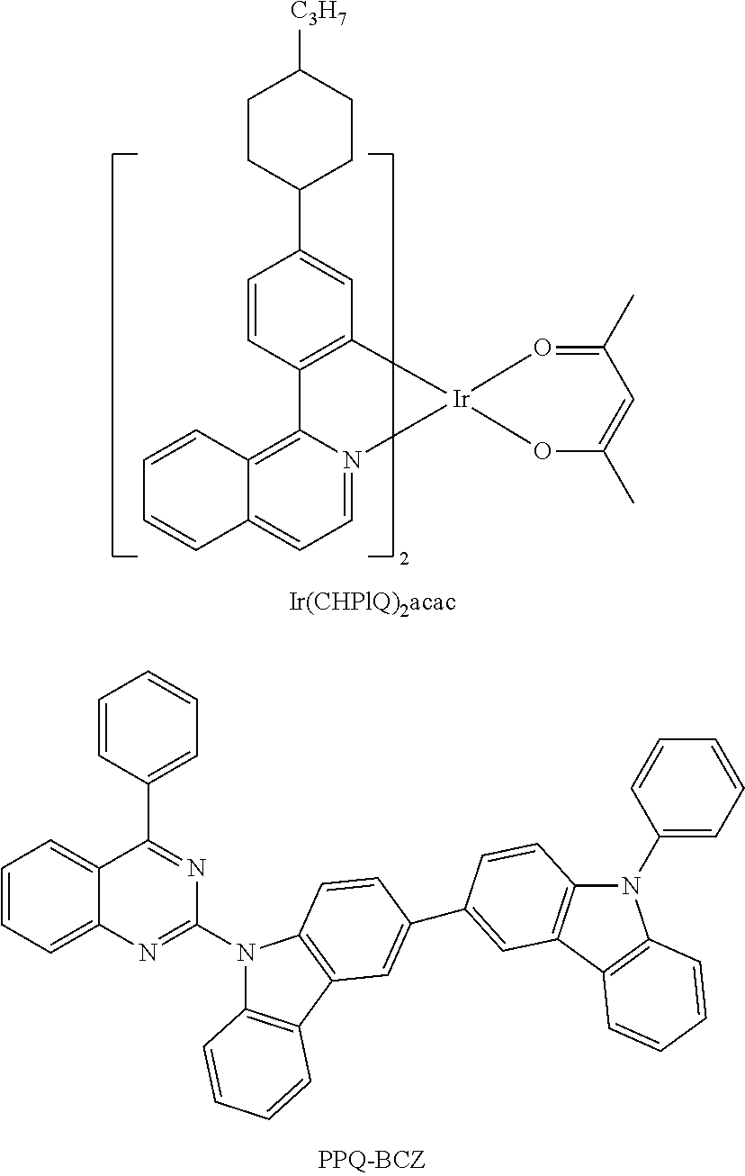
| TABLE 2 |
| Performance test results of the resulting devices OLED-4 to OLED-6 |
| Host | Electric | ||||||
| material | Turn-on | current | |||||
| DEVICES | Compound | voltage | density | Brightness | EQE | CIE | T95 |
| No. | formula | (V) | (mA/cm2) | (Cd/m2) | (%) | (x, y) | (hour) |
| OLED-4 | A30 | 3.8 | 3.6 | 1000 | 21.4 | 0.67, | 5000 |
| 0.32 | |||||||
| OLED-5 | A57 | 3.6 | 3.4 | 1000 | 21.6 | 0.67, | 6000 |
| 0.31 | |||||||
| OLED-6 | PPQ-BCZ | 4.4 | 3.8 | 1000 | 20.0 | 0.68, | 5000 |
| 0.32 | |||||||
Claims (7)


Applications Claiming Priority (3)
| Application Number | Priority Date | Filing Date | Title |
|---|---|---|---|
| CN201710193446.4 | 2017-03-28 | ||
| CN201710193446 | 2017-03-28 | ||
| CN201710193446.4A CN106967060B (en) | 2017-03-28 | 2017-03-28 | Series of carbazole derivatives and application thereof |
Publications (2)
| Publication Number | Publication Date |
|---|---|
| US20180282277A1 US20180282277A1 (en) | 2018-10-04 |
| US10577325B2 true US10577325B2 (en) | 2020-03-03 |
Family
ID=59336622
Family Applications (1)
| Application Number | Title | Priority Date | Filing Date |
|---|---|---|---|
| US15/714,295 Active 2038-03-15 US10577325B2 (en) | 2017-03-28 | 2017-09-25 | Method for preparing a series of carbazole derivatives and use thereof in organic light-emitting diodes |
Country Status (2)
| Country | Link |
|---|---|
| US (1) | US10577325B2 (en) |
| CN (1) | CN106967060B (en) |
Families Citing this family (17)
| Publication number | Priority date | Publication date | Assignee | Title |
|---|---|---|---|---|
| CN109516980B (en) * | 2017-09-20 | 2020-12-11 | 邱天隆 | Bipolar materials and organic light emitting diode elements |
| KR102431667B1 (en) * | 2017-09-21 | 2022-08-12 | 삼성디스플레이 주식회사 | Heterocyclic compound, organic electroluminescence device and organic electroluminescence display device including the same |
| CN107793398B (en) * | 2017-11-09 | 2021-02-26 | 石家庄诚志永华显示材料有限公司 | A thermally induced delayed fluorescent material |
| CN110386930B (en) * | 2018-04-18 | 2023-07-14 | 香港科技大学 | Aggregation-induced luminescence compound, preparation method and application thereof |
| CN108831997A (en) * | 2018-06-26 | 2018-11-16 | 东莞理工学院 | Sandwich structure memory device and preparation method thereof |
| US20200207752A1 (en) * | 2018-12-26 | 2020-07-02 | Int Tech Co., Ltd. | Organic electroluminescent compound and organic electroluminescent device containing the same |
| CN109678844B (en) * | 2019-02-02 | 2021-04-27 | 苏州科技大学 | Orange red photo-thermal activation delayed fluorescence material and organic electroluminescent device |
| CN110563633B (en) * | 2019-08-30 | 2022-11-08 | 武汉华星光电半导体显示技术有限公司 | Blue-light thermal activation delay fluorescent material, preparation method thereof and electroluminescent device |
| CN112552301A (en) * | 2019-09-26 | 2021-03-26 | 广州华睿光电材料有限公司 | Indoloquinone organic compound and application thereof |
| CN110964019B (en) * | 2019-12-12 | 2021-05-04 | 西安瑞联新材料股份有限公司 | Compound taking 6-phenyl-6H-indolo [2,3-b ] quinoxaline as receptor and application thereof |
| CN113248451B (en) * | 2020-04-27 | 2023-04-28 | 广东聚华印刷显示技术有限公司 | Quinoxaline compound, polymer, organic electronic device and display panel |
| KR102883831B1 (en) * | 2021-04-27 | 2025-11-11 | 삼성디스플레이 주식회사 | Condensed cylic compound, light emitting device including the condensed cyclic compound and electronic apparatus including the light emitting device |
| CN117800994B (en) * | 2022-09-23 | 2025-06-13 | 江苏三月科技股份有限公司 | A boron-containing organic compound containing a carbazole-fluorene structure and an organic electroluminescent device prepared therefrom |
| GB202315830D0 (en) | 2023-10-16 | 2023-11-29 | Univ Court Univ St Andrews | Compounds |
| CN118125993A (en) * | 2024-02-07 | 2024-06-04 | 西北师范大学 | BTD-type fluorescent small molecule compounds with solvent-induced color effect |
| CN118084957B (en) * | 2024-04-19 | 2024-08-23 | 季华恒烨(佛山)电子材料有限公司 | Boron-nitrogen compound and application thereof |
| CN119798286B (en) * | 2025-03-12 | 2025-06-20 | 南京邮电大学 | Benzoxazole ring core-based thermal activation delayed fluorescence luminescent material and preparation method and application thereof |
Citations (4)
| Publication number | Priority date | Publication date | Assignee | Title |
|---|---|---|---|---|
| WO2011093309A1 (en) * | 2010-01-28 | 2011-08-04 | コニカミノルタホールディングス株式会社 | Organic photoelectric conversion element |
| CN103936653A (en) * | 2013-12-12 | 2014-07-23 | 石家庄诚志永华显示材料有限公司 | Benzo carbazoles OLED material, its preparation method and its application |
| JP2015129240A (en) * | 2014-01-08 | 2015-07-16 | 国立大学法人九州大学 | Luminescent materials, organic light emitting devices and compounds |
| EP3010068A1 (en) * | 2014-10-17 | 2016-04-20 | Samsung Display Co., Ltd. | Organic light-emitting device |
Family Cites Families (4)
| Publication number | Priority date | Publication date | Assignee | Title |
|---|---|---|---|---|
| JP3945032B2 (en) * | 1998-08-10 | 2007-07-18 | 東洋インキ製造株式会社 | Luminescent material for organic electroluminescence device and organic electroluminescence device using the same |
| JP2001097962A (en) * | 1999-09-29 | 2001-04-10 | Fuji Photo Film Co Ltd | Trisbenzoazole compound |
| US10355222B2 (en) * | 2015-02-06 | 2019-07-16 | Universal Display Corporation | Organic electroluminescent materials and devices |
| CN106432051B (en) * | 2016-09-20 | 2019-02-22 | 长春海谱润斯科技有限公司 | A kind of carbazole analog derivative and its preparation method and application |
-
2017
- 2017-03-28 CN CN201710193446.4A patent/CN106967060B/en active Active
- 2017-09-25 US US15/714,295 patent/US10577325B2/en active Active
Patent Citations (4)
| Publication number | Priority date | Publication date | Assignee | Title |
|---|---|---|---|---|
| WO2011093309A1 (en) * | 2010-01-28 | 2011-08-04 | コニカミノルタホールディングス株式会社 | Organic photoelectric conversion element |
| CN103936653A (en) * | 2013-12-12 | 2014-07-23 | 石家庄诚志永华显示材料有限公司 | Benzo carbazoles OLED material, its preparation method and its application |
| JP2015129240A (en) * | 2014-01-08 | 2015-07-16 | 国立大学法人九州大学 | Luminescent materials, organic light emitting devices and compounds |
| EP3010068A1 (en) * | 2014-10-17 | 2016-04-20 | Samsung Display Co., Ltd. | Organic light-emitting device |
Non-Patent Citations (5)
| Title |
|---|
| Computer-generated English-language translation of CN 103936653A. * |
| Machine Translation of JP 2015-129240-A. * |
| SciFinder Search (Sep. 20, 2019). * |
| SciFinder Searches (May 8, 2019). * |
| Yu et al., Dye and Pigments 141 (2017) 325-332. * |
Also Published As
| Publication number | Publication date |
|---|---|
| CN106967060B (en) | 2020-09-11 |
| CN106967060A (en) | 2017-07-21 |
| US20180282277A1 (en) | 2018-10-04 |
Similar Documents
| Publication | Publication Date | Title |
|---|---|---|
| US10577325B2 (en) | Method for preparing a series of carbazole derivatives and use thereof in organic light-emitting diodes | |
| KR101041642B1 (en) | Compound for organic electroluminescent device and organic electroluminescent device | |
| KR101311934B1 (en) | Composition for organic photoelectric device and organic photoelectric device using the same | |
| US8344368B2 (en) | Fused cyclic compound and organic electronic device | |
| TWI452114B (en) | Organic electroluminescent element compounds and organic electroluminescent elements | |
| KR101247626B1 (en) | Compounds for organic photoelectric device and organic photoelectric device containing the same | |
| US7906228B2 (en) | Compounds for electronic material and organic electronic device using the same | |
| US11462694B2 (en) | Imidazole derivative, material and organic light-emitting device comprising the same | |
| CN109678844B (en) | Orange red photo-thermal activation delayed fluorescence material and organic electroluminescent device | |
| JP6067873B2 (en) | Novel compound and organic electronic device using the same | |
| JP2015516973A (en) | Nitrogen-containing heterocyclic compound and organic electronic device containing the same | |
| JP6275720B2 (en) | Nitrogen-containing heterocyclic compound and organic electronic device containing the same | |
| KR20190011463A (en) | Compound for organic electronic element, organic electronic element comprising the same, and electronic device thereof | |
| KR20100001274A (en) | Organic compound, and organic photoelectric device including the same | |
| KR20130020399A (en) | Compound for organic optoelectronic device, organic light emitting diode including the same and display including the organic light emitting diode | |
| CN111777516A (en) | An organic light-emitting compound and its preparation method and application | |
| US20180222910A1 (en) | Compound for organic electrical element, organic electrical element using compound, and electronic device therefor | |
| US20190093009A1 (en) | Delayed fluorescence compound and organic electroluminescent device using the same | |
| KR20110065978A (en) | Red phosphorescent host compound and organic light emitting device using the same | |
| KR20140083412A (en) | Red Phosphorescent Host Material and Organic Electroluminescent Device Using the Same | |
| CN115417872B (en) | A condensed ring compound, a luminescent composition containing indolecarbazole, and an organic electroluminescent device | |
| CN112939993B (en) | A kind of benzopyran light-emitting auxiliary material and preparation method thereof and organic electroluminescent device | |
| CN107880031B (en) | Azabenzene-based compounds and their applications in organic electroluminescent devices | |
| CN111116670B (en) | Organic metal iridium complex and preparation method and application thereof | |
| CN111808125A (en) | An organic compound, organic electroluminescent material and application thereof |
Legal Events
| Date | Code | Title | Description |
|---|---|---|---|
| FEPP | Fee payment procedure |
Free format text: ENTITY STATUS SET TO UNDISCOUNTED (ORIGINAL EVENT CODE: BIG.); ENTITY STATUS OF PATENT OWNER: LARGE ENTITY |
|
| AS | Assignment |
Owner name: SHIJIAZHUANG CHENGZHI YONGHUA DISPLAY MATERIAL CO., LTD., CHINA Free format text: ASSIGNMENT OF ASSIGNORS INTEREST;ASSIGNORS:CAO, JIANHUA;WANG, SHIBO;HUA, RUIMAO;REEL/FRAME:043712/0981 Effective date: 20170919 Owner name: SHIJIAZHUANG CHENGZHI YONGHUA DISPLAY MATERIAL CO. Free format text: ASSIGNMENT OF ASSIGNORS INTEREST;ASSIGNORS:CAO, JIANHUA;WANG, SHIBO;HUA, RUIMAO;REEL/FRAME:043712/0981 Effective date: 20170919 |
|
| STPP | Information on status: patent application and granting procedure in general |
Free format text: DOCKETED NEW CASE - READY FOR EXAMINATION |
|
| STPP | Information on status: patent application and granting procedure in general |
Free format text: NON FINAL ACTION MAILED |
|
| STPP | Information on status: patent application and granting procedure in general |
Free format text: RESPONSE TO NON-FINAL OFFICE ACTION ENTERED AND FORWARDED TO EXAMINER |
|
| STPP | Information on status: patent application and granting procedure in general |
Free format text: FINAL REJECTION MAILED |
|
| STPP | Information on status: patent application and granting procedure in general |
Free format text: NOTICE OF ALLOWANCE MAILED -- APPLICATION RECEIVED IN OFFICE OF PUBLICATIONS |
|
| STPP | Information on status: patent application and granting procedure in general |
Free format text: PUBLICATIONS -- ISSUE FEE PAYMENT VERIFIED |
|
| STCF | Information on status: patent grant |
Free format text: PATENTED CASE |
|
| MAFP | Maintenance fee payment |
Free format text: PAYMENT OF MAINTENANCE FEE, 4TH YEAR, LARGE ENTITY (ORIGINAL EVENT CODE: M1551); ENTITY STATUS OF PATENT OWNER: LARGE ENTITY Year of fee payment: 4 |