US10573209B2 - Systems and methods for indirect threshold voltage sensing in an electronic display - Google Patents
Systems and methods for indirect threshold voltage sensing in an electronic display Download PDFInfo
- Publication number
- US10573209B2 US10573209B2 US15/273,444 US201615273444A US10573209B2 US 10573209 B2 US10573209 B2 US 10573209B2 US 201615273444 A US201615273444 A US 201615273444A US 10573209 B2 US10573209 B2 US 10573209B2
- Authority
- US
- United States
- Prior art keywords
- current
- voltage
- sensing
- pixel
- capacitor
- Prior art date
- Legal status (The legal status is an assumption and is not a legal conclusion. Google has not performed a legal analysis and makes no representation as to the accuracy of the status listed.)
- Active, expires
Links
- 238000000034 method Methods 0.000 title claims description 86
- 239000003990 capacitor Substances 0.000 claims description 111
- 238000003860 storage Methods 0.000 claims description 22
- 238000004364 calculation method Methods 0.000 claims description 4
- 238000007599 discharging Methods 0.000 claims 1
- 241000750042 Vini Species 0.000 description 52
- 238000010586 diagram Methods 0.000 description 51
- 238000005259 measurement Methods 0.000 description 15
- 238000005070 sampling Methods 0.000 description 13
- 238000012545 processing Methods 0.000 description 12
- 230000007704 transition Effects 0.000 description 12
- 230000000644 propagated effect Effects 0.000 description 8
- 230000008569 process Effects 0.000 description 6
- 230000010354 integration Effects 0.000 description 5
- 238000004519 manufacturing process Methods 0.000 description 5
- 239000011159 matrix material Substances 0.000 description 5
- 230000006399 behavior Effects 0.000 description 4
- 230000001413 cellular effect Effects 0.000 description 4
- 230000008859 change Effects 0.000 description 4
- 238000004088 simulation Methods 0.000 description 4
- 230000004913 activation Effects 0.000 description 3
- 230000008901 benefit Effects 0.000 description 3
- 230000002596 correlated effect Effects 0.000 description 3
- 238000011156 evaluation Methods 0.000 description 3
- 230000006870 function Effects 0.000 description 3
- 238000012986 modification Methods 0.000 description 3
- 230000004048 modification Effects 0.000 description 3
- 230000008672 reprogramming Effects 0.000 description 3
- 101100127285 Drosophila melanogaster unc-104 gene Proteins 0.000 description 2
- 230000032683 aging Effects 0.000 description 2
- 238000004422 calculation algorithm Methods 0.000 description 2
- 230000015556 catabolic process Effects 0.000 description 2
- 230000000875 corresponding effect Effects 0.000 description 2
- 230000007423 decrease Effects 0.000 description 2
- 238000006731 degradation reaction Methods 0.000 description 2
- 238000013461 design Methods 0.000 description 2
- 238000011161 development Methods 0.000 description 2
- 230000018109 developmental process Effects 0.000 description 2
- 238000000691 measurement method Methods 0.000 description 2
- 230000003071 parasitic effect Effects 0.000 description 2
- 238000012546 transfer Methods 0.000 description 2
- 230000009286 beneficial effect Effects 0.000 description 1
- 238000006243 chemical reaction Methods 0.000 description 1
- 238000004590 computer program Methods 0.000 description 1
- 230000009849 deactivation Effects 0.000 description 1
- 230000003247 decreasing effect Effects 0.000 description 1
- 230000007547 defect Effects 0.000 description 1
- 230000000694 effects Effects 0.000 description 1
- 230000007774 longterm Effects 0.000 description 1
- 238000012806 monitoring device Methods 0.000 description 1
- 230000003287 optical effect Effects 0.000 description 1
- 230000002093 peripheral effect Effects 0.000 description 1
- 238000003825 pressing Methods 0.000 description 1
- 239000010409 thin film Substances 0.000 description 1
Images


Classifications
-
- G—PHYSICS
- G09—EDUCATION; CRYPTOGRAPHY; DISPLAY; ADVERTISING; SEALS
- G09G—ARRANGEMENTS OR CIRCUITS FOR CONTROL OF INDICATING DEVICES USING STATIC MEANS TO PRESENT VARIABLE INFORMATION
- G09G3/00—Control arrangements or circuits, of interest only in connection with visual indicators other than cathode-ray tubes
- G09G3/006—Electronic inspection or testing of displays and display drivers, e.g. of LED or LCD displays
-
- G—PHYSICS
- G09—EDUCATION; CRYPTOGRAPHY; DISPLAY; ADVERTISING; SEALS
- G09G—ARRANGEMENTS OR CIRCUITS FOR CONTROL OF INDICATING DEVICES USING STATIC MEANS TO PRESENT VARIABLE INFORMATION
- G09G3/00—Control arrangements or circuits, of interest only in connection with visual indicators other than cathode-ray tubes
- G09G3/20—Control arrangements or circuits, of interest only in connection with visual indicators other than cathode-ray tubes for presentation of an assembly of a number of characters, e.g. a page, by composing the assembly by combination of individual elements arranged in a matrix no fixed position being assigned to or needed to be assigned to the individual characters or partial characters
- G09G3/22—Control arrangements or circuits, of interest only in connection with visual indicators other than cathode-ray tubes for presentation of an assembly of a number of characters, e.g. a page, by composing the assembly by combination of individual elements arranged in a matrix no fixed position being assigned to or needed to be assigned to the individual characters or partial characters using controlled light sources
- G09G3/30—Control arrangements or circuits, of interest only in connection with visual indicators other than cathode-ray tubes for presentation of an assembly of a number of characters, e.g. a page, by composing the assembly by combination of individual elements arranged in a matrix no fixed position being assigned to or needed to be assigned to the individual characters or partial characters using controlled light sources using electroluminescent panels
- G09G3/32—Control arrangements or circuits, of interest only in connection with visual indicators other than cathode-ray tubes for presentation of an assembly of a number of characters, e.g. a page, by composing the assembly by combination of individual elements arranged in a matrix no fixed position being assigned to or needed to be assigned to the individual characters or partial characters using controlled light sources using electroluminescent panels semiconductive, e.g. using light-emitting diodes [LED]
- G09G3/3208—Control arrangements or circuits, of interest only in connection with visual indicators other than cathode-ray tubes for presentation of an assembly of a number of characters, e.g. a page, by composing the assembly by combination of individual elements arranged in a matrix no fixed position being assigned to or needed to be assigned to the individual characters or partial characters using controlled light sources using electroluminescent panels semiconductive, e.g. using light-emitting diodes [LED] organic, e.g. using organic light-emitting diodes [OLED]
- G09G3/3225—Control arrangements or circuits, of interest only in connection with visual indicators other than cathode-ray tubes for presentation of an assembly of a number of characters, e.g. a page, by composing the assembly by combination of individual elements arranged in a matrix no fixed position being assigned to or needed to be assigned to the individual characters or partial characters using controlled light sources using electroluminescent panels semiconductive, e.g. using light-emitting diodes [LED] organic, e.g. using organic light-emitting diodes [OLED] using an active matrix
- G09G3/3233—Control arrangements or circuits, of interest only in connection with visual indicators other than cathode-ray tubes for presentation of an assembly of a number of characters, e.g. a page, by composing the assembly by combination of individual elements arranged in a matrix no fixed position being assigned to or needed to be assigned to the individual characters or partial characters using controlled light sources using electroluminescent panels semiconductive, e.g. using light-emitting diodes [LED] organic, e.g. using organic light-emitting diodes [OLED] using an active matrix with pixel circuitry controlling the current through the light-emitting element
-
- G—PHYSICS
- G09—EDUCATION; CRYPTOGRAPHY; DISPLAY; ADVERTISING; SEALS
- G09G—ARRANGEMENTS OR CIRCUITS FOR CONTROL OF INDICATING DEVICES USING STATIC MEANS TO PRESENT VARIABLE INFORMATION
- G09G3/00—Control arrangements or circuits, of interest only in connection with visual indicators other than cathode-ray tubes
- G09G3/20—Control arrangements or circuits, of interest only in connection with visual indicators other than cathode-ray tubes for presentation of an assembly of a number of characters, e.g. a page, by composing the assembly by combination of individual elements arranged in a matrix no fixed position being assigned to or needed to be assigned to the individual characters or partial characters
- G09G3/22—Control arrangements or circuits, of interest only in connection with visual indicators other than cathode-ray tubes for presentation of an assembly of a number of characters, e.g. a page, by composing the assembly by combination of individual elements arranged in a matrix no fixed position being assigned to or needed to be assigned to the individual characters or partial characters using controlled light sources
- G09G3/30—Control arrangements or circuits, of interest only in connection with visual indicators other than cathode-ray tubes for presentation of an assembly of a number of characters, e.g. a page, by composing the assembly by combination of individual elements arranged in a matrix no fixed position being assigned to or needed to be assigned to the individual characters or partial characters using controlled light sources using electroluminescent panels
- G09G3/32—Control arrangements or circuits, of interest only in connection with visual indicators other than cathode-ray tubes for presentation of an assembly of a number of characters, e.g. a page, by composing the assembly by combination of individual elements arranged in a matrix no fixed position being assigned to or needed to be assigned to the individual characters or partial characters using controlled light sources using electroluminescent panels semiconductive, e.g. using light-emitting diodes [LED]
- G09G3/3208—Control arrangements or circuits, of interest only in connection with visual indicators other than cathode-ray tubes for presentation of an assembly of a number of characters, e.g. a page, by composing the assembly by combination of individual elements arranged in a matrix no fixed position being assigned to or needed to be assigned to the individual characters or partial characters using controlled light sources using electroluminescent panels semiconductive, e.g. using light-emitting diodes [LED] organic, e.g. using organic light-emitting diodes [OLED]
- G09G3/3266—Details of drivers for scan electrodes
-
- G—PHYSICS
- G09—EDUCATION; CRYPTOGRAPHY; DISPLAY; ADVERTISING; SEALS
- G09G—ARRANGEMENTS OR CIRCUITS FOR CONTROL OF INDICATING DEVICES USING STATIC MEANS TO PRESENT VARIABLE INFORMATION
- G09G3/00—Control arrangements or circuits, of interest only in connection with visual indicators other than cathode-ray tubes
- G09G3/20—Control arrangements or circuits, of interest only in connection with visual indicators other than cathode-ray tubes for presentation of an assembly of a number of characters, e.g. a page, by composing the assembly by combination of individual elements arranged in a matrix no fixed position being assigned to or needed to be assigned to the individual characters or partial characters
- G09G3/22—Control arrangements or circuits, of interest only in connection with visual indicators other than cathode-ray tubes for presentation of an assembly of a number of characters, e.g. a page, by composing the assembly by combination of individual elements arranged in a matrix no fixed position being assigned to or needed to be assigned to the individual characters or partial characters using controlled light sources
- G09G3/30—Control arrangements or circuits, of interest only in connection with visual indicators other than cathode-ray tubes for presentation of an assembly of a number of characters, e.g. a page, by composing the assembly by combination of individual elements arranged in a matrix no fixed position being assigned to or needed to be assigned to the individual characters or partial characters using controlled light sources using electroluminescent panels
- G09G3/32—Control arrangements or circuits, of interest only in connection with visual indicators other than cathode-ray tubes for presentation of an assembly of a number of characters, e.g. a page, by composing the assembly by combination of individual elements arranged in a matrix no fixed position being assigned to or needed to be assigned to the individual characters or partial characters using controlled light sources using electroluminescent panels semiconductive, e.g. using light-emitting diodes [LED]
- G09G3/3208—Control arrangements or circuits, of interest only in connection with visual indicators other than cathode-ray tubes for presentation of an assembly of a number of characters, e.g. a page, by composing the assembly by combination of individual elements arranged in a matrix no fixed position being assigned to or needed to be assigned to the individual characters or partial characters using controlled light sources using electroluminescent panels semiconductive, e.g. using light-emitting diodes [LED] organic, e.g. using organic light-emitting diodes [OLED]
- G09G3/3275—Details of drivers for data electrodes
- G09G3/3291—Details of drivers for data electrodes in which the data driver supplies a variable data voltage for setting the current through, or the voltage across, the light-emitting elements
-
- G—PHYSICS
- G09—EDUCATION; CRYPTOGRAPHY; DISPLAY; ADVERTISING; SEALS
- G09G—ARRANGEMENTS OR CIRCUITS FOR CONTROL OF INDICATING DEVICES USING STATIC MEANS TO PRESENT VARIABLE INFORMATION
- G09G2300/00—Aspects of the constitution of display devices
- G09G2300/08—Active matrix structure, i.e. with use of active elements, inclusive of non-linear two terminal elements, in the pixels together with light emitting or modulating elements
- G09G2300/0809—Several active elements per pixel in active matrix panels
- G09G2300/0814—Several active elements per pixel in active matrix panels used for selection purposes, e.g. logical AND for partial update
-
- G—PHYSICS
- G09—EDUCATION; CRYPTOGRAPHY; DISPLAY; ADVERTISING; SEALS
- G09G—ARRANGEMENTS OR CIRCUITS FOR CONTROL OF INDICATING DEVICES USING STATIC MEANS TO PRESENT VARIABLE INFORMATION
- G09G2300/00—Aspects of the constitution of display devices
- G09G2300/08—Active matrix structure, i.e. with use of active elements, inclusive of non-linear two terminal elements, in the pixels together with light emitting or modulating elements
- G09G2300/0809—Several active elements per pixel in active matrix panels
- G09G2300/0819—Several active elements per pixel in active matrix panels used for counteracting undesired variations, e.g. feedback or autozeroing
-
- G—PHYSICS
- G09—EDUCATION; CRYPTOGRAPHY; DISPLAY; ADVERTISING; SEALS
- G09G—ARRANGEMENTS OR CIRCUITS FOR CONTROL OF INDICATING DEVICES USING STATIC MEANS TO PRESENT VARIABLE INFORMATION
- G09G2310/00—Command of the display device
- G09G2310/02—Addressing, scanning or driving the display screen or processing steps related thereto
- G09G2310/0202—Addressing of scan or signal lines
-
- G—PHYSICS
- G09—EDUCATION; CRYPTOGRAPHY; DISPLAY; ADVERTISING; SEALS
- G09G—ARRANGEMENTS OR CIRCUITS FOR CONTROL OF INDICATING DEVICES USING STATIC MEANS TO PRESENT VARIABLE INFORMATION
- G09G2310/00—Command of the display device
- G09G2310/02—Addressing, scanning or driving the display screen or processing steps related thereto
- G09G2310/0264—Details of driving circuits
- G09G2310/0291—Details of output amplifiers or buffers arranged for use in a driving circuit
-
- G—PHYSICS
- G09—EDUCATION; CRYPTOGRAPHY; DISPLAY; ADVERTISING; SEALS
- G09G—ARRANGEMENTS OR CIRCUITS FOR CONTROL OF INDICATING DEVICES USING STATIC MEANS TO PRESENT VARIABLE INFORMATION
- G09G2310/00—Command of the display device
- G09G2310/06—Details of flat display driving waveforms
- G09G2310/061—Details of flat display driving waveforms for resetting or blanking
-
- G—PHYSICS
- G09—EDUCATION; CRYPTOGRAPHY; DISPLAY; ADVERTISING; SEALS
- G09G—ARRANGEMENTS OR CIRCUITS FOR CONTROL OF INDICATING DEVICES USING STATIC MEANS TO PRESENT VARIABLE INFORMATION
- G09G2320/00—Control of display operating conditions
- G09G2320/02—Improving the quality of display appearance
- G09G2320/0233—Improving the luminance or brightness uniformity across the screen
-
- G—PHYSICS
- G09—EDUCATION; CRYPTOGRAPHY; DISPLAY; ADVERTISING; SEALS
- G09G—ARRANGEMENTS OR CIRCUITS FOR CONTROL OF INDICATING DEVICES USING STATIC MEANS TO PRESENT VARIABLE INFORMATION
- G09G2320/00—Control of display operating conditions
- G09G2320/02—Improving the quality of display appearance
- G09G2320/029—Improving the quality of display appearance by monitoring one or more pixels in the display panel, e.g. by monitoring a fixed reference pixel
- G09G2320/0295—Improving the quality of display appearance by monitoring one or more pixels in the display panel, e.g. by monitoring a fixed reference pixel by monitoring each display pixel
-
- G—PHYSICS
- G09—EDUCATION; CRYPTOGRAPHY; DISPLAY; ADVERTISING; SEALS
- G09G—ARRANGEMENTS OR CIRCUITS FOR CONTROL OF INDICATING DEVICES USING STATIC MEANS TO PRESENT VARIABLE INFORMATION
- G09G2320/00—Control of display operating conditions
- G09G2320/04—Maintaining the quality of display appearance
- G09G2320/043—Preventing or counteracting the effects of ageing
- G09G2320/045—Compensation of drifts in the characteristics of light emitting or modulating elements
-
- G—PHYSICS
- G09—EDUCATION; CRYPTOGRAPHY; DISPLAY; ADVERTISING; SEALS
- G09G—ARRANGEMENTS OR CIRCUITS FOR CONTROL OF INDICATING DEVICES USING STATIC MEANS TO PRESENT VARIABLE INFORMATION
- G09G2330/00—Aspects of power supply; Aspects of display protection and defect management
- G09G2330/12—Test circuits or failure detection circuits included in a display system, as permanent part thereof
Definitions
- This disclosure relates to indirect threshold voltage sensing in display panels. More specifically, the current disclosure provides systems and methods that indirectly sense threshold voltages of pixel circuitry using multiple current or voltage measurements.
- Threshold voltage e.g., Vth
- Vth Threshold voltage
- Vth changes in a display may be caused by many different factors.
- Vth changes may be caused by temperature changes of the display, an aging of the display (e.g., aging of the thin-film-transistors (TFTs)), display processes, component manufacturing defects, and many other factors.
- TFTs thin-film-transistors
- Vth shifting To counter-act image degradation caused by Vth shifting, it may be desirable to implement compensation for the Vth shifting.
- processing time and memory availability to determine and compensate for Vth may become more and more limited. For example, compensating for varying Vth values on individual pixels may become burdensome on the display system. Further, timing constraints for determining Vth values and compensating for the Vth values may result in timing limitations on compensation circuits.
- compensation circuitry may be used to counter-act negative artifacts cause by threshold voltage (Vth) variations throughout a collection of pixels in the display.
- Vth values may be determined based on indirect current or charge sensing techniques. In such a manner, the negative artifacts provided by Vth variations may be avoided by compensating for the Vth variations through columns of pixels rather than at an individual pixel level.
- indirectly calculated Vth values may be used in compensation logic that adjusts columns of pixels within the display based upon the Vth values that are received by the compensation logic.
- FIG. 1 is a schematic block diagram of an electronic device including a display, in accordance with an embodiment
- FIG. 2 is a perspective view of a notebook computer representing an embodiment of the electronic device of FIG. 1 , in accordance with an embodiment
- FIG. 3 is a front view of a hand-held device representing another embodiment of the electronic device of FIG. 1 , in accordance with an embodiment
- FIG. 4 is a front view of another hand-held device representing another embodiment of the electronic device of FIG. 1 , in accordance with an embodiment
- FIG. 5 is a front view of a desktop computer representing another embodiment of the electronic device of FIG. 1 , in accordance with an embodiment
- FIG. 6 is a front view of a wearable electronic device representing another embodiment of the electronic device of FIG. 1 , in accordance with an embodiment
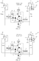
- FIG. 7 is a circuit diagram illustrating a portion of a matrix of pixels of the display of FIG. 1 , in accordance with an embodiment
- FIG. 8 is a circuit diagram illustrating an organic light emitting diode pixel capable of operating in the matrix of pixels of FIG. 7 , in accordance with an embodiment
- FIG. 9 is a schematic diagram, illustrating a sampling phase 900 , in accordance with an embodiment
- FIG. 10 is a schematic diagram, illustrating a transition phase 1000 , in accordance with an embodiment
- FIG. 11 is a schematic diagram, illustrating a read out phase 1100 , in accordance with an embodiment
- FIGS. 12-15 are schematic diagrams, illustrating a progression of phases of pixels 62 useful to determine Vth, in accordance with certain embodiments
- FIG. 15A is a schematic diagram, illustrating a timing diagram of the phases of FIGS. 12-15 , in accordance with an embodiment
- FIG. 16 illustrates an initialization phase, in accordance with an embodiment
- FIG. 17 is a schematic diagram, illustrating a pre-charge phase, in accordance with an embodiment
- FIG. 18 is a schematic diagram, illustrating an evaluation phase, in accordance with an embodiment
- FIG. 19 is a schematic diagram, illustrating a timing diagram for the three phases of FIGS. 17-19 , in accordance with an embodiment
- FIGS. 20-23 are schematic diagrams, illustrating phases of a technique for measuring LED (e.g. OLED) voltage (Voled) on the Vini line, in accordance with certain embodiments;
- LED e.g. OLED
- Voled Voled
- FIG. 24 is a schematic diagram illustrating a timing diagram for the techniques described in FIGS. 20-23 , in accordance with an embodiment
- FIG. 25 is a schematic diagram, illustrating a normal operation mode for OLED pixel circuitry 62 , in accordance with an embodiment
- FIG. 26 is a schematic diagram, illustrating sensing parameters of the OLED pixel circuitry that may allow an OLED current to be measured, in accordance with an embodiment
- FIG. 27 is a schematic diagram of simulated data, illustrating simulated current sensing, using the techniques described in FIGS. 25 and 26 , in accordance with an embodiment
- FIG. 28A is a circuit diagram of an initialization phase for measuring a threshold voltage of an organic light emitting diode pixel, in accordance with an embodiment
- FIG. 28B is a circuit diagram of a sampling phase for measuring the threshold voltage of the organic light emitting diode pixel, in accordance with an embodiment
- FIG. 28C is a circuit diagram of a readout phase for measuring the threshold voltage of the organic light emitting diode pixel, in accordance with an embodiment
- FIG. 28D is a timing diagram of the phases illustrated in FIGS. 28A-28C , in accordance with an embodiment
- FIG. 29A is a circuit diagram of a sampling phase for measuring an organic light emitting diode voltage of an organic light emitting diode pixel, in accordance with an embodiment
- FIG. 29B is a circuit diagram of a readout phase for measuring the organic light emitting diode voltage of the organic light emitting diode pixel, in accordance with an embodiment
- FIG. 29C is a timing diagram of the phases illustrated in FIGS. 29A and 29B , in accordance with an embodiment
- FIG. 30 is a circuit diagram of a second method for measuring the organic light emitting diode voltage of the organic light emitting diode pixel, in accordance with an embodiment
- FIG. 31 is a circuit diagram of a charge sensing analog front-end circuit that converts output voltage values from an analog representation to a digital representation, in accordance with an embodiment
- FIG. 32 is a schematic diagram illustrating circuitry that implements both the charge sensing techniques and the current sensing techniques, in accordance with an embodiment
- FIG. 33A is a chart of a simulation of an output voltage of an organic light emitting diode pixel settling over time, in accordance with an embodiment
- FIG. 33B is a chart of a simulation of a settling percentage of the output voltage of FIG. 33A over time, in accordance with an embodiment
- FIG. 34 is a circuit diagram including a sensing channel to indirectly sense a threshold voltage of a pixel, in accordance with an embodiment
- FIG. 35 is a method of calculating a threshold voltage from the circuit diagram of FIG. 34 , in accordance with an embodiment
- FIG. 36 is a schematic diagram of the sensing channel of FIG. 34 during a programming phase of measuring current leakage of the pixel of FIG. 34 , in accordance with an embodiment
- FIG. 37 is a schematic diagram of the sensing channel of FIG. 34 during a current leakage sensing phase of the pixel of FIG. 34 , in accordance with an embodiment
- FIG. 38 is a schematic diagram of the sensing channel of FIG. 34 during a pixel current and current leakage sensing phase of the pixel of FIG. 34 , in accordance with an embodiment
- FIG. 39 is a method of sensing a leakage measurement from the sensing channel of FIGS. 36-38 , in accordance with an embodiment
- FIG. 40 is an alternative method of sensing a leakage measurement from the sensing channel of FIGS. 36-38 , in accordance with an embodiment.
- FIG. 41 is a timing diagram of the method of FIG. 40 , in accordance with an embodiment.
- This disclosure relates to near-real time compensation for threshold voltage (Vth) shifts, light-emitting diode (LED) (e.g., organic LEDs (OLEDs)) voltage (Voled) shifts, and/or LED (e.g., organic LEDs (Oleds)) current (Ioled) shifts that may occur in display panels. More specifically, the current embodiments describe techniques for re-using many components of a display panel's circuitry to provide external-to-the-pixel measurement of Vth, Voled, and/or Ioled. These measurements may be provided to compensation logic that alters display output based upon shifts in the Vth, Voled, and/or Ioled.
- Vth threshold voltage
- LED light-emitting diode
- LED organic LEDs
- Ioled organic LEDs
- an electronic device 10 may include, among other things, a processor core complex 12 having one or more processor(s), memory 14 , nonvolatile storage 16 , a display 18 input structures 22 , an input/output (I/O) interface 24 , network interfaces 26 , and a power source 28 .
- the various functional blocks shown in FIG. 1 may include hardware elements (including circuitry), software elements (including computer code stored on a computer-readable medium) or a combination of both hardware and software elements. It should be noted that FIG. 1 is merely one example of a particular implementation and is intended to illustrate the types of components that may be present in electronic device 10 .
- the electronic device 10 may represent a block diagram of the notebook computer depicted in FIG. 2 , the handheld device depicted in FIG. 3 , the desktop computer depicted in FIG. 4 , the wearable electronic device depicted in FIG. 5 , or similar devices.
- the processor core complex 12 and/or other data processing circuitry may be generally referred to herein as “data processing circuitry.” Such data processing circuitry may be embodied wholly or in part as software, firmware, hardware, or any combination thereof.
- the data processing circuitry may be a single contained processing module or may be incorporated wholly or partially within any of the other elements within the electronic device 10 .
- the processor core complex 12 and/or other data processing circuitry may be operably coupled with the memory 14 and the nonvolatile memory 16 to perform various algorithms.
- Such programs or instructions executed by the processor core complex 12 may be stored in any suitable article of manufacture that may include one or more tangible, computer-readable media at least collectively storing the instructions or routines, such as the memory 14 and the nonvolatile storage 16 .
- the memory 14 and the nonvolatile storage 16 may include any suitable articles of manufacture for storing data and executable instructions, such as random-access memory, read-only memory, rewritable flash memory, hard drives, and optical discs.
- programs (e.g., an operating system) encoded on such a computer program product may also include instructions that may be executed by the processor core complex 12 to enable the electronic device 10 to provide various functionalities.
- the display 18 may include pixels such as organic light emitting diodes (OLEDs), micro-light-emitting-diodes ( ⁇ -LEDs), or any other light emitting diodes (LEDs).
- OLEDs organic light emitting diodes
- ⁇ -LEDs micro-light-emitting-diodes
- LEDs light emitting diodes
- the display 18 is not limited to a particular pixel type, as the circuitry and methods disclosed herein may apply to any pixel type. Accordingly, while particular pixel structures may be illustrated in the present disclosure, the present disclosure may relate to a broad range of lighting components and/or pixel circuits within display devices.
- the input structures 22 of the electronic device 10 may enable a user to interact with the electronic device 10 (e.g., pressing a button to increase or decrease a volume level).
- the I/O interface 24 may enable electronic device 10 to interface with various other electronic devices, as may the network interfaces 26 .
- the network interfaces 26 may include, for example, interfaces for a personal area network (PAN), such as a Bluetooth network, for a local area network (LAN) or wireless local area network (WLAN), such as an 802.11x Wi-Fi network, and/or for a wide area network (WAN), such as a 3rd generation (3G) cellular network, 4th generation (4G) cellular network, or long term evolution (LTE) cellular network.
- PAN personal area network
- LAN local area network
- WLAN wireless local area network
- WAN wide area network
- 3G 3rd generation
- 4G 4th generation
- LTE long term evolution
- the network interface 26 may also include interfaces for, for example, broadband fixed wireless access networks (WiMAX), mobile broadband Wireless networks (mobile WiMAX), asynchronous digital subscriber lines (e.g., 15SL, VDSL), digital video broadcasting-terrestrial (DVB-T) and its extension DVB Handheld (DVB-H), ultra Wideband (UWB), alternating current ( 14 ) power lines, and so forth.
- WiMAX broadband fixed wireless access networks
- mobile WiMAX mobile broadband Wireless networks
- asynchronous digital subscriber lines e.g., 15SL, VDSL
- DVD-T digital video broadcasting-terrestrial
- DVD-H extension DVB Handheld
- UWB ultra Wideband
- alternating current ( 14 ) power lines and so forth.
- the electronic device 10 may take the form of a computer, a portable electronic device, a wearable electronic device, or other type of electronic device.
- Such computers may include computers that are generally portable (such as laptop, notebook, and tablet computers) as well as computers that are generally used in one place (such as conventional desktop computers, workstations and/or servers).
- the electronic device 10 in the form of a computer may be a model of a MacBook®, MacBook® Pro, MacBook Air®, iMac®, Mac® mini, or Mac Pro® available from Apple Inc.
- the electronic device 10 taking the form of a notebook computer 30 A, is illustrated in FIG. 2 in accordance with one embodiment of the present disclosure.
- the depicted computer 30 A may include a housing or enclosure 32 , a display 18 , input structures 22 , and ports of an I/O interface 24 .
- the input structures 22 (such as a keyboard and/or touchpad) may be used to interact with the computer 39 , such as to start, control, or operate a GUI or applications running on computer 39 .
- a keyboard and/or touchpad may allow a user to navigate a user interface or application interface displayed on display 18 .
- FIG. 3 depicts a front view of a handheld device 30 B, which represents one embodiment of the electronic device 10 .
- the handheld device 34 may represent, for example, a portable phone, a media player, a personal data organizer, a handheld game platform, or any combination of such devices.
- the handheld device 34 may be a model of an iPod® or iPhone® available from Apple Inc. of Cupertino, Calif.
- the handheld device 30 B may include an enclosure 36 to protect interior components from physical damage and to shield them from electromagnetic interference.
- the enclosure 36 may surround the display 18 , which may display indicator icons 39 .
- the indicator icons 39 may indicate, among other things, a cellular signal strength, Bluetooth connection, and/or battery life.
- the I/O interfaces 24 may open through the enclosure 36 and may include, for example, an I/O port for a hard wired connection for charging and/or content manipulation using a standard connector and protocol, such as the Lightning connector provided by Apple Inc., a universal service bus (USB), or other similar connector and protocol.
- User input structures 42 may allow a user to control the handheld device 30 B.
- the input structure 40 may activate or deactivate the handheld device 30 B
- the input structure 42 may navigate user interface to a home screen, a user-configurable application screen, and/or activate a voice-recognition feature of the handheld device 30 B
- the input structures 42 may provide volume control, or may toggle between vibrate and ring modes.
- the input structures 42 may also include a microphone may obtain a user's voice for various voice-related features, and a speaker may enable audio playback and/or certain phone capabilities.
- the input structures 42 may also include a headphone input may provide a connection to external speakers and/or headphones.
- FIG. 4 depicts a front view of another handheld device 30 C, which represents another embodiment of the electronic device 10 .
- the handheld device 30 C may represent, for example, a tablet computer, or one of various portable computing devices.
- the handheld device 30 C may be a tablet-sized embodiment of the electronic device 10 , which may be, for example, a model of an iPad® available from Apple Inc. of Cupertino, Calif.
- a computer 30 D may represent another embodiment of the electronic device 10 of FIG. 1 .
- the computer 30 D may be any computer, such as a desktop computer, a server, or a notebook computer, but may also be a standalone media player or video gaming machine.
- the computer 30 D may be an iMac®, a MacBook®, or other similar device by Apple Inc.
- the computer 30 D may also represent a personal computer (PC) by another manufacturer.
- a similar enclosure 36 may be provided to protect and enclose internal components of the computer 30 D such as the display 18 .
- a user of the computer 30 D may interact with the computer 30 D using various peripheral input devices, such as the input structures 22 or mouse 38 , which may connect to the computer 30 D via a wired and/or wireless I/O interface 24 .
- FIG. 6 depicts a wearable electronic device 30 E representing another embodiment of the electronic device 10 of FIG. 1 that may be configured to operate using the techniques described herein.
- the wearable electronic device 30 E which may include a wristband 43 , may be an Apple Watch® by Apple, Inc.
- the wearable electronic device 30 E may include any wearable electronic device such as, for example, a wearable exercise monitoring device (e.g., pedometer, accelerometer, heart rate monitor), or other device by another manufacturer.
- the display 18 of the wearable electronic device 30 E may include a touch screen, which may allow users to interact with a user interface of the wearable electronic device 30 E.
- the display 18 for the electronic device 10 may include a matrix of pixels that contain light emitting circuitry. Accordingly, FIG. 7 illustrates a circuit diagram including a portion of a matrix of pixels of the display 18 .
- the display 18 may include a display panel 60 .
- the display panel 60 may include multiple unit pixels 62 arranged as an array or matrix defining multiple rows and columns of the unit pixels 62 that collectively form a viewable region of the display 18 in which an image may be displayed.
- each unit pixel 62 may be defined by the intersection of rows and columns, represented here by the illustrated gate lines 64 (also referred to as “scanning lines”) and data lines 66 (also referred to as “source lines”), respectively.
- power supply lines 68 may provide power to each of the unit pixels 62 .
- each data line 66 and gate line 64 may include hundreds or even thousands of such unit pixels 62 .
- each data line 66 which may define a column of the pixel array, may include 768 unit pixels
- each gate line 64 which may define a row of the pixel array, may include 1024 groups of unit pixels with each group including a red, blue, and green pixel, thus totaling 3072 unit pixels per gate line 64 .
- the panel 60 may have a resolution of 480 ⁇ 320 or 960 ⁇ 640.
- the unit pixels 62 a , 62 b , and 62 c may represent a group of pixels having a red pixel ( 62 a ), a blue pixel ( 62 b ), and a green pixel ( 62 c ).
- the group of unit pixels 62 d , 62 e , and 62 f may be arranged in a similar manner.
- pixel may refer to a group of adjacent different-colored pixels (e.g., a red pixel, blue pixel, and green pixel), with each of the individual colored pixels in the group being referred to as a “sub-pixel.”
- the display 18 also includes a source driver integrated circuit (IC) 90 , which may include a chip, such as a processor or ASIC, configured to control various aspects of the display 18 and panel 60 .
- the source driver IC 90 may receive image data 92 from the processor core complex 12 and send corresponding image signals to the unit pixels 62 of the panel 60 .
- the source driver IC 90 may also be coupled to a gate driver IC 94 , which may be configured to provide/remove gate activation signals to activate/deactivate rows of unit pixels 62 via the gate lines 64 .
- the source driver IC 90 may include a timing controller that determines and sends timing information 96 to the gate driver IC 94 to facilitate activation and deactivation of individual rows of unit pixels 62 .
- timing information may be provided to the gate driver IC 94 in some other manner (e.g., using a timing controller that is separate from the source driver IC 90 ).
- FIG. 7 depicts only a single source driver IC 90 , it should be appreciated that other embodiments may utilize multiple source driver ICs 90 to provide image signals to the unit pixels 62 .
- additional embodiments may include multiple source driver ICs 90 disposed along one or more edges of the panel 60 , with each source driver IC 90 being configured to control a subset of the data lines 66 and/or gate lines 64 .
- the source driver IC 90 receives image data 92 from the processor core complex 12 or a discrete display controller and, based on the received data, outputs signals to control the unit pixels 62 .
- circuitry within the unit pixels 62 may complete a circuit between a power supply 98 and light elements of the unit pixels 62 .
- measurement circuitry 100 may be positioned within the source driver IC 90 to read various voltage and current characteristics of the display 18 , as discussed in detail below.
- FIG. 8 is a schematic diagram of the unit pixel 62 in an OLED display 18 .
- the unit pixel 62 includes a driving thin-film transistor (TFT) 102 , two scanning TFTs 104 and 106 , an emitter TFT 108 , and a storage capacitor 110 in a 4T1C pixel configuration.
- the source emitter TFT 108 may couple between the power supply 98 and the driving TFT 102 .
- the emitter TFT 108 which may receive a control signal from a timing controller 112 , controls the application of the power supply to the driving TFT 102 .
- the driving TFT 102 may be electrically coupled between the emitter TFT 108 and an organic light emitting diode (OLED) 114 . Accordingly, the driving TFT 102 controls the application of the power supply from the emitter TFT 108 to the OLED 114 .
- the scanning TFT 104 may be electrically coupled between a data line 66 a , which carries a data voltage (Vdata) 116 , and a gate 118 of the driving TFT 102 .
- a gate 120 of the scanning TFT 104 may be electrically coupled to a first gate line 64 a , which may receive a first scanning signal 121 from the gate driver IC 94 .
- Each of the TFTs 102 , 104 , 106 , and 108 function as switching elements and may be activated and deactivated (e.g., switched on and off) for a predetermined period based upon the respective presence or absence of a gate activation signal (also referred to as a scanning signal) at the gates of the TFTs 102 , 104 , 106 , and 108 .
- a gate activation signal also referred to as a scanning signal
- a storage capacitor 110 may be electrically coupled to a drain 122 of the scanning TFT 104 and a drain 124 of the scanning transistor 106 .
- a source 126 of the scanning TFT 106 may be electrically coupled to a second data line 66 B, which carries an initialization voltage (Vini) 128 .
- a gate 130 of the scanning TFT 106 may be coupled to a second gate line 64 b , which may receive a second scanning signal 132 from the gate driver IC 94 .
- the source driver IC 90 and the gate driver IC 94 may respectively supply voltage to the scanning TFT 104 to charge the storage capacitor 110 .
- the storage capacitor 110 may drive the gate 118 of the driving TFT 102 to provide a current from the power supply 98 to the OLED 114 of the unit pixel 62 .
- the color of a particular unit pixel depends on the color of the corresponding OLED 114 .
- the above-described process may be repeated for each row of pixels 62 in the panel 60 to reproduce image data 92 as a viewable image on the display 18 .
- FIG. 8 depicts the OLED 114
- any other type of lighting element may also be used in place of the OLED 114 for the methods described herein.
- the first scanning signal 121 may generally control when the data line 66 a is applied to the driving TFT 102 , and, in turn, when the power supply 98 is supplied to the OLED 114 .
- the second scanning signal 132 may generally control when the capacitor 110 and the OLED 114 couple to the second data line 66 B.
- the measurement circuitry 100 may observe various operating parameters of the unit pixels 62 , as discussed in detail below.
- FIGS. 9-11 illustrate three basic phases to complete charge sensing.
- FIG. 9 illustrates a sampling phase 900
- FIG. 10 illustrates a transition phase 1000
- FIG. 11 illustrates a read out phase 1100 .
- FIG. 9 illustrates a sampling phase 900
- FIG. 10 illustrates a transition phase 1000
- FIG. 11 illustrates a read out phase 1100 .
- a capacitor 902 is shorted (e.g., via a switch 904 ). Accordingly, the output voltage Vout of an amplifier 906 may equal V 0 .
- the top plate of a capacitor 908 may be V 0 as well.
- transition phase 1000 the short of the capacitor 902 is removed (e.g., by opening the switch 904 ).
- this phase 1000 there are no signal changes, so the voltages remain constant with phase 900 .
- the charge represented by box 910 remains constant.
- phase 1100 a step down voltage 1102 is applied, resulting in the bottom plate voltage going lower to V 1 .
- a current 1104 flows from the capacitor 902 .
- the top plate of capacitor 908 is equal to the left plate of capacitor 902 .
- additional charge 1108 may be present.
- charge sensing techniques described in phases 900 - 1100 of FIGS. 9-11 may be used to obtain operational parameters on existing display circuitry with relatively few hardware modifications.
- FIGS. 12-15 illustrate a progression of phases of pixels 62 useful to determine Vth.
- FIG. 15A provides a timing diagram of the phases of FIGS. 12-15 . For clarity, each of these FIGS. will be discussed together.
- a first amplifier 1202 may provide a Vdata voltage 116 on line 66 a .
- a second amplifier 1204 may provide a Vini voltage 128 on line 66 B.
- First scanning signal 121 may be connected (e.g., via gate 120 ).
- second scanning signal 132 may be connected (e.g., via gate 130 ).
- a switch (SW 0 ) 1201 may short a feedback capacitor (Cf) 1203 . Accordingly, the Vdata voltage 116 may propagate through the TFT 104 and the Vini voltage 128 may propagate through the TFT 106 .
- the Vini voltage 128 may be low, such that the OLED 114 may be off (as indicated by the X 1206 ). Further, the timing controller 112 may set the emitter TFT 108 to OFF (as indicated by X 1208 ) via the emission signal 1210 , disconnecting the power supply 98 .
- column PH 1 illustrates the timing of the first scanning signal 121 , the second scanning signal 132 , the emission signal 1210 , and a switching signal for switch 1201 . Further, voltage values are symbolized for second node 1212 and third node 1214 . As indicated, second node 1212 is equal to the propagated Vdata voltage 116 . The third node 1214 is equal to the propagated Vini voltage 128 .
- the second phase may initiate sampling in the unit pixel 62 .
- the second scanning signal 132 may be disconnected (as indicated by the X 1302 ).
- the driving transistor 102 may be coupled with the power supply 98 by turning on the emission signal 1210 , which results in turning the emitter TFT 108 ON.
- the signals other than the second scanning signal 132 and the emission signal 1210 remain consistent with the signals of phase 1200 .
- the third node 1214 increases to equal the propagated Vdata voltage 116 minus Vth.
- the voltage at the third node 1214 may be low enough, such that the OLED 114 remains OFF (as illustrated by the X 1206 ). Thus, no visible light may be seen at the OLED 114 .
- a DC change phase may occur.
- the first scanning signal 121 is a low logic signal, as indicated by X 1402 .
- the second scanning signal 132 is a high logic signal.
- the emission signal 1210 is a low logic signal, resulting in emitter TFT 108 being turned OFF, as indicated by X 1404 .
- the switch 1201 remains closed, shorting the feedback capacitor Cf 1203 . With these settings, the second node 1212 voltage drops from Vdata voltage 116 to Vini voltage 128 plus Vth. Further, the voltage of the third node 1214 transitions to Vini 128 .
- Vth may be calculated using the voltages of node 2 1212 and node 3 1214 at this phase 1400 . However, to remove parasitic capacitance, the Vth is propagated through the next phase 1500 , where the second node 1212 transitions to Vdata 116 .
- the first scanning signal 121 is a high logic signal. Accordingly, the second node 1212 transitions to Vdata 116 . Further, the second scanning signal 132 remains high. Additionally, the emission signal 1210 remains low. Further, the switch 1201 is opened, removing the short of the capacitor 1203 . Accordingly, as illustrated in FIG. 15A , the third node transitions to Vini 128 . Further, a voltage output (Vout) 1502 transitions to Vini ⁇ (Vdata ⁇ Vini ⁇ Vth) or 2Vini+Vth ⁇ Vdata. Because Vini 128 and Vdata 116 are known constants, the Vout 1502 may be used to determine the Vth.
- the Vini signal 128 may be a global initialization signal used across an entire display 18 panel. Accordingly, in such embodiments, Vth values for only one pixel may be read at a time. In some embodiments, additional Vini signals 128 ′ may be used to read out Vth values more efficiently. For example, separate Vini signals 128 ′ may be provided per column of pixels in the display 18 . However, such embodiments may still not provide parallel Red, Green, and Blue read outs, because the Vini signals 128 ′ may be shared for red columns, shared for blue columns, and shared for green columns. Further, these embodiments may utilize timeout blanking periods to power the pixels and to receive the read out information, which may reduce efficiency.
- reading the Vth signal over the Vini line may provide several benefits.
- this technique may be easily calibrated, as the reference values (e.g., Vdata 116 and/or Vini 128 ) are known constants that may be used to single out the Vth value. Accordingly, Vth shift calibrations may be implemented without significant processing constraints.
- FIGS. 12-15 illustrate a 4T1C (4 transistor, 1 capacitor) unit pixel 62 circuit
- the current techniques may be utilized on a number of other pixel circuitry types.
- the current techniques may utilize existing hardware, reducing additional hardware overhead.
- existing driving amplifiers may be used in the current techniques.
- a minimal amount of hardware may be added to the circuitry (e.g., the switch 1201 and capacitor 1203 ). This added hardware may be added to the timing controller 112 , which may be less costly than providing hardware in the unit pixel 62 circuitry and/or the display 18 panel.
- the global buses are not toggled. When toggled, the global buses may require a capacitor charge, which may consume additional power. However, since the Vdata 116 and Vini 128 voltages remain constant, the capacitors do not need to be charged, thus the power consumption for determining the Vth using the current techniques may be negligible.
- FIGS. 16-18 illustrate a three-phase (e.g., phases 1600 , 1700 , and 1800 ) technique utilizing 5T1C (5 transistors and 1 capacitor) unit pixel 62 circuitry.
- FIG. 16 illustrates an initialization phase
- FIG. 17 illustrates a pre-charge phase
- FIG. 18 illustrates an evaluation phase.
- FIG. 19 illustrates a timing diagram 1900 for the three phases 1600 , 1700 , and 1800 .
- the current technique may reduce the number of phases to three phases, as compared to the technique described in FIGS. 12-15A , which includes four phases.
- the current technique also utilizes a third transistor 1602 and a third scanning signal 1604 .
- the third transistor 1602 may create a feedback voltage that may replace the sampling phase 1300 described in FIG. 13 .
- the initialization phase 1600 of FIG. 17 is very similar to the initialization phase 1200 of FIG. 12 .
- the first scanning signal 121 and second scanning signal 132 are high logic signals.
- the third scanning signal 1604 and emitter signal 1210 are low. These settings result in Vdata 116 at the second node 1212 .
- the third node is Vini 128 and remains at Vini 128 for each of the subsequent phases 1700 and 1800 .
- the first scanning signal 121 and the emitter signal 1210 may be low, while the second and third scanning signals 132 and 1604 are high logic signals. These changes cause the second node 1212 to transition to Vini 128 minus Vth.
- Vth may be calculated using the voltages of node 2 1212 and node 3 1214 at this phase 17 . However, to remove parasitic capacitance, the Vth is propagated through the next phase, where the second node 1212 transitions to Vdata 116 .
- the first scanning signal 121 and second scanning signal 132 are high logic signals.
- the third scanning signal 1604 and the Emitter signal 1210 are low.
- the switch 1201 may be opened, such that the short of the capacitor 1203 is removed. These changes cause the second node 1212 to drop to Vdata 116 .
- FIGS. 20-23 illustrate phases of a technique for measuring LED (e.g. OLED) voltage (Voled) on the Vini line 66 B.
- FIG. 24 provides a timing diagram 2400 for the techniques described in FIGS. 20-23 . For clarity, these figures will be discussed together.
- the first scanning signal 121 and the emitter signal 1210 are high logic signals and the switch 1201 is closed. This results in TFTs 108 and 104 turning ON. TFT 106 is turned OFF (as represented by X 2002 ). Node 2 1212 is set to Vdata 116 and Node 3 is set to Voled. The OLED 114 is ON.
- the first scanning signal 121 and second scanning signal 132 are low.
- the emitter signal 1210 and the switch 1201 remain high, continuing to short the capacitor 1203 and providing voltage to the OLED 114 .
- Node 2 1212 becomes Vdata 116 .
- Node 3 1214 becomes Voled.
- the OLED 114 remains ON.
- the first scanning signal 121 is low, turning OFF transistor 104 (as indicated by X 2202 ). Further, the second scanning signal 132 the emitter signal 1210 are high and the switch 1201 is closed, resulting in continued shorting of the capacitor 1203 , and the transistors 108 and 106 to turn ON.
- the OLED may not be ON (as indicated by X 2204 ) because the voltage may flow along line 66 B. Node 2 1212 becomes voltage Vini 128 +Vdata 116 —Voled. Node 3 voltage becomes Vini 128 .
- the first scanning signal 121 and second scanning signal 132 are high logic signals. This results in TFTs 104 and 106 turning ON.
- the emitter signal 1210 is a low logic signal, resulting in transistor 108 turning OFF (as indicated by X 2302 ).
- the switch 1201 is opened, removing the short to the capacitor 1203 (as indicated by X 2304 ). Additionally, as a result of these settings, the OLED 114 does not receive power from the power supply 98 and is, thus, turned OFF (as indicated by X 2306 ).
- the voltage output (Vout) 2308 may be calculated as 2Vini ⁇ Voled. Accordingly, because Vini 128 is known, Voled may be calculated.
- FIG. 25 illustrates a normal operation mode for OLED unit pixel 62 circuitry.
- FIG. 26 illustrates sensing parameters of the OLED unit pixel 62 circuitry that may allow an OLED current to be measured, using relatively little additional hardware to the display 18 circuitry.
- FIG. 27 illustrates simulated data, illustrating simulated current sensing, using the techniques described in FIGS. 25 and 26 . These figures will be discussed together for clarity.
- FIG. 25 illustrates a normal operational mode 2500 , where OLED 114 is emitting light.
- the TFT 108 is ON, causing voltage to flow from the power supply 98 to the OLED 114 .
- the switch 1201 is closed, shorting the capacitor 1203 .
- the voltage output (Vout) 2502 may be connected to a third amplifier 2504 .
- the third amplifier 2504 may be used to provide a voltage comparison (Vcmp) 2506 , which may be used in conjunction with the counter 2508 and a clock 2510 (e.g. a timing controller clock) to measure the Ioled.
- Vcmp voltage comparison
- FIG. 26 illustrates a current sensing mode 2600 used to obtain the Ioled value.
- the short to the capacitor 1203 is removed, by opening the switch 1201 .
- the second scanning signal 132 are high logic signals, resulting in voltage flow through the TFT 106 . This results in current flow through the path indicated by Iout 2601 .
- the third amplifier 2504 may provide a voltage comparison Vcmp 2506 .
- the Vcmp 2506 may compare the Vout 2502 with a pre-defined voltage trip value Vtrip 2602 . More specifically, the third amplifier 2504 may provide a first value via Vcmp 2506 when Vout 2502 does not cross Vtrip 2602 . However, upon Vout 2502 crossing Vtrip 2602 , a second value may be provided via Vcmp 2606 .
- the counter 2508 and clock 2510 may be used in the calculation of Ioled.
- the counter 2508 may calculate a number of clock cycles of the clock 2510 between Vcmp 2506 transitioning from the first value to the second value after the bout 2601 is provided.
- the counter 2508 may count a number of clock cycles between transitioning between Vout 2502 to Vtrip 2602 .
- ⁇ V may be calculated as Vout 2502 ⁇ Vtrip 2602 .
- Vout 2502 is equal to Vini 128 .
- the Vout 2502 is initially equal to Vini 128 , resulting in a first value 2701 (e.g., a low value) at Vcmp 2506 .
- a first value 2701 e.g., a low value
- the output current Iout 2601 flows to the capacitor 1203 .
- the Vout 2502 begins to transition downward.
- a second value 2706 is output by Vcmp 2506 .
- ⁇ V may be calculated as 0.5V (e.g., the difference between the Vout 2502 and Vtrip 2602 ).
- ⁇ t is calculated as 74.5 us (e.g., the difference between times 2704 and 2702 ).
- FIGS. 28A-28C illustrate a progression of phases of unit pixels 62 useful to determine Vth.
- FIG. 28D provides a timing diagram of the phases of FIGS. 28A-28C . For clarity, each of these FIGS. will be discussed together.
- a first amplifier 142 may provide a Vdata voltage 116 on the first data line 66 a .
- a second amplifier 150 may provide a Vini voltage 128 on the second data line 66 B.
- the first scanning signal 121 may provide a signal to the gate 120 of the scanning TFT 104 to activate the scanning TFT 104 .
- the second scanning signal 132 may provide a signal to the gate 130 of the scanning TFT 106 to activate the scanning TFT 106 .
- a switch 144 may short a feedback capacitor 146 coupled across a negative terminal 145 and an output 147 of the amplifier 142 .
- the Vdata voltage 116 may propagate through the scanning TFT 104 , and the Vini voltage 128 may propagate through the gate 130 . Additionally, the Vini voltage may be sufficiently low, such that the OLED 114 remains in an OFF state, as indicated by the X 152 over the OLED 114 . Further, the timing controller 112 may set the emitter TFT 108 to OFF (as indicated by the X 154 ) via the emission signal 156 , disconnecting the power supply 98 from the unit pixel 62 .
- column PH 1 of a timing diagram 163 illustrates the timing of the first scanning signal 121 , the second scanning signal 132 , the emission signal 156 , Vdata voltage 116 , Vini voltage 128 , and voltage output (Vout) voltage 158 . Further, voltage values are symbolized for second node 160 and third node 162 . As indicated, second node 160 is equal to the propagated Vdata voltage 116 . The third node 162 is equal to the propagated Vini voltage 128 .
- the second phase 164 may initiate sampling in the unit pixel 62 .
- the second scanning signal 132 may be provide a low signal to the scanning TFT 106 (as indicated by column PH 2 of FIG. 28D ).
- the emitter TFT 108 may couple the power supply 98 to the driving TFT 102 when the emission signal 156 is a high signal.
- the signals other than the second scanning signal 132 and the emission signal 156 remain consistent with the signals of the first phase 140 .
- the third node 162 becomes equal the propagated Vdata voltage 116 minus a threshold voltage (Vth of the OLED 114 .
- the voltage at the third node 162 may be low enough, such that the OLED 114 remains OFF (as illustrated by the X 152 ). Thus, no visible light may be seen at the OLED 114 .
- a readout phase may occur.
- the first scanning signal 121 remains high, and the second scanning signal 132 becomes a high logic value.
- the emission signal 156 is a low logic value, resulting in the emitter TFT 108 being turned OFF, as indicated by X 172 .
- the switch 144 is opened, removing the short of the feedback capacitor 146 .
- the second node 160 remains at the Vdata voltage 116
- the third node 162 becomes the Vini voltage 128 .
- Determining the value of Vth along the first data line 66 a may result in simple calibration of the unit pixel 62 .
- the reference values e.g., Vdata 116 and/or Vini 128
- Vth shift calibrations may be implemented without significant processing constraints.
- this charge transfer technique may apply to a number of pixel types that include a capacitor 110 .
- FIGS. 28A-28C illustrate a 4T1C (4 transistor, 1 capacitor) unit pixel 62 circuit, the current techniques may be utilized on a number of other pixel circuitry types that include a capacitor.
- the current techniques may utilize existing hardware, reducing additional hardware overhead.
- existing driving amplifiers may be used in the current techniques (e.g., driving amplifiers within the timing controller 112 or the source driver IC 90 ).
- a minimal amount of hardware may be added to the circuitry (e.g., the switch 144 and capacitor 146 ). This added hardware may be added to the timing controller 112 , which may be less costly than providing hardware in the pixel circuitry 62 and/or the display 18 panel.
- the global buses are not toggled. When toggled, the global buses may require a capacitor charge, which may consume additional power. However, since the Vdata 116 and Vini 128 voltages remain constant, the capacitors do not need to be charged, thus the power consumption for determining the Vth using the current techniques may be negligible.
- the Vth for the red, green, and blue pixel units 62 may be calculated in parallel. Accordingly, there is flexibility in reading out the Vth values for the different color pixel units 62 separately. Therefore, determining the Vth from the first data line 66 a may increase efficiency for the display 18 as a whole.
- Vdata 116 and Vini 128 may be selected in such a manner that the OLED 114 remains inactive throughout the technique described above.
- the Vth value while not known exactly prior to solving for Vth, may be around 1.5V. Accordingly, Vdata 116 may be less than 1.5V and greater than 0V.
- FIGS. 29A-29B illustrate phases of a technique for measuring LED (e.g. OLED) voltage (Voled) on the first data line 66 a .
- FIG. 29C provides a timing diagram 200 for the techniques described in FIGS. 29A-29B . For clarity, these figures will be discussed together.
- the first scanning signal 121 and the emitter signal 156 both have high logic values, and the switch 144 is set to closed. This results in TFTs 108 and 104 turning ON. Additionally, the TFT 106 is turned OFF (as represented by X 182 ). Accordingly, the second node 160 registers a voltage of Vdata 116 and the third node 162 registers the Voled value. Additionally, the OLED 114 is ON.
- the first scanning signal 121 and second scanning signal 132 provide high voltages to the scanning TFTs 104 and 106 .
- the emitter signal 156 provides a low signal to the emitting TFT 108 (as represented by X 192 ) and the switch 144 is opened (as represented by X 194 ), removing the short around the capacitor 146 .
- the OLED 114 no longer receives power from the power supply 98 and is, thus, turned OFF (as represented by X 196 ).
- the second node 160 continues to register the voltage of Vdata 116 . Further, the voltage of the third node 162 decreases from Voled to Vini 128 .
- the voltage output (Vout) 158 may be read.
- the value of Vout 158 in this configuration is equal to Vdata ⁇ Vini+Voled. Accordingly, because Vout 158 , Vdata 116 , and Vini 128 are known, Voled may be calculated. Similar to the Vth measurement technique discussed above, the Voled measurement technique provides simple calibration, applies to most pixel circuits, provides parallel readout for red, blue, and green pixel units 62 , and consumes a low amount of power.
- a value of Vdata 116 may be selected in such a manner that Vdata 116 is greater than the Voled value added to the Vth value.
- the value of Voled plus Vth may be approximately 3.5V depending on the specific OLED 114 used in the pixel unit 62 and the age of the OLED 114 .
- the value of Vini 128 may be a value less than 0V, and the value of Vout 158 may be greater than 0V. Accordingly, Vout 158 may be approximately 5.5V when Vdata 116 is selected as slightly greater than 3.5V and Vini is selected as slightly less than 0V.
- a pixel unit 62 that uses a second method 210 to measure the Voled value is illustrated.
- a measuring TFT 212 is disposed within the pixel unit 62 .
- the value of Vdata 116 may remain greater than the voltage at the third node 162 . Accordingly, the measuring TFT 212 remains in an OFF state.
- the Vdata 116 value is pulled down using a current source 214 coupled to a fourth node 216 . By pulling down the voltage at the fourth node 216 , Vout, measured at the fourth node 216 , may equal Voled ⁇ Vth+Vod.
- FIG. 31 illustrates charge sensing analog front-end circuitry 218 that converts values of Vout 158 from an analog representation to a digital representation.
- the charge sensing analog front-end circuitry 218 may be implemented within any of the measurement circuitry 100 , the timing controller 112 , or the source driver IC 90 .
- a signal representing a value of Vout 158 may be provided to a negative terminal 219 of a comparator 220 .
- a positive terminal 221 of the comparator 220 may receive a signal (Vdac 222 ) from a gamma digital-to-analog converter (DAC) 226 , which converts a digital signal from a successive approximation register (SAR) logic device 224 .
- Vdac 222 a signal from a gamma digital-to-analog converter (DAC) 226 , which converts a digital signal from a successive approximation register (SAR) logic device 224 .
- SAR successive approximation register
- the SAR logic device 224 provides a starting voltage indication to the gamma DAC 226 for a voltage comparison between the analog value of Vout 158 and the value of Vdac 222 .
- the comparator 220 makes a determination of whether Vout 158 is greater or less than Vdac 222 .
- the result of this comparison, digital output voltage (DOUTV) 228 is fed back to the SAR logic device 224 .
- DOUTV 228 digital output voltage
- the SAR logic device 224 may alter a most significant bit, and the SAR logic device 224 may continue to the next bit and performs the comparison again.
- the SAR logic device 224 may provide a digital indication of the value of Vout 158 .
- the charge sensing analog front-end circuitry 218 may be used when determining digital representations of Vout 158 values for calculating either or both of the Vth values or Voled values, as described above.
- charge sensing techniques and the current sensing techniques may be combined.
- charge sensing analog front-end (AFE) circuitry 3202 utilizes the Vdata 116 line 66 a and current sensing analog front-end (AFE) circuitry 3204 utilizes the Vini 128 line 66 B.
- the charge sensing AFE circuitry 3204 may use the first amplifier 1202 , the switch 144 , the capacitor 146 , a voltage output Vout 158 , SAR logic 224 , Gamma D/A 226 , and a comparator 220 to determine charges of the pixel circuitry 62 .
- the charges may be determined in accordance with the discussion provided in FIG. 31 .
- the current sensing AFE 3204 may use the switch 1201 , the capacitor 1203 , the second amplifier 1204 , a third amplifier 2504 , the Vini input 128 , a Vtrip input 2602 , a Vcmp output 2506 , a counter 2508 , and a clock 2510 to determine a current of the pixel circuitry 62 .
- the current may be determined, via the current sensing AFE circuitry 3204 , in accordance with the discussion provided in FIGS. 25-27 .
- certain components may be shared between the charge sensing AFE circuitry 3202 and the current sensing AFE circuitry 3202 .
- the comparator 220 and amplifier 2504 may be shared, while retaining the ability to determine both charges via the circuitry 3202 and the current from the circuitry 3204 .
- charts 240 and 242 provide a simulation of Vout 158 settling over time 244 .
- the chart 240 includes a vertical axis representing Vout 158 and a horizontal axis representing the time 244 .
- the three curves 246 , 248 , and 250 provided in the chart 240 represent the Vout settling when the threshold voltages are Vth, Vth+0.2V, and Vth ⁇ 0.2V, respectively.
- the curves 246 , 248 , and 250 depict settling of the Vout 158 value over time when the pixel unit 62 is in a readout phase.
- the settling behavior may be characterized. Accordingly, with settling behavior representing a first order linear system, an accurate prediction of the settled value of Vout 158 may be determined much earlier than when waiting for the system to settle.
- FIG. 33B depicts the chart 242 including a vertical axis representing a settling percentage 252 and a horizontal axis representing the time 244 .
- the three Vth values generally track the same curve 254 over the time 244 . Accordingly, regardless of the Vth value, the settling behavior, as indicated in FIGS. 33A and 33B is very similar. For example, the difference in settling behavior may be 2% or less.
- Vout 158 To extrapolate the settled value of Vout 158 , a measurement of Vout 158 may be taken early in the settling period at a time T 1 . Because the settling percentage 252 is known at time T 1 , a value at settled time T 2 for Vout 158 may be extrapolated from the reading at time T 1 . Once the extrapolated value for Vout at the settled time T 2 is measured, the calculation for Vth, Voled, or Ioled may occur.
- Vdata_new Vdata_old+k_Vth*Vth_variation
- FIG. 34 illustrates a circuit diagram 3400 including a sensing channel 3402 to indirectly sense a threshold voltage of the pixel 62 .
- FIG. 35 is a method 3420 for indirectly measuring the threshold voltage of the pixel 62 with the sensing channel 3402 of FIG. 34 .
- FIGS. 34 and 35 will be discussed together.
- FIG. 34 is a schematic diagram of the unit pixel 62 and the sensing channel 3402 .
- the data voltage source 116 is amplified by an amplifier 1202 within the gate driver IC 94 .
- the initialization voltage source 128 is amplified by the amplifier 1204 within the source driver IC 90 .
- the sensing channel 3402 may be included within the source driver IC 90 , or, in other embodiments, the sensing channel 3402 may be separate from the source driver IC 90 .
- each column of the unit pixels 62 may include a sensing channel 3402 that is separate from sensing channels of other columns of the unit pixels 62 .
- the sensing channel 3402 may include a sensing amplifier 3404 and an integrating capacitor 3406 .
- the sensing amplifier 3404 and the integrating capacitor 3406 function together as an amplifier integrator capable of producing a signal that is representative of a current coming from the unit pixel 62 .
- the sensing channel 3402 may include several switches 3408 , 3410 , and 3412 . The switches may perform various functions such as resetting the integrating capacitor 3406 and programming the integrating capacitor 3406 , as described in greater detail below.
- the initialization voltage source 128 from the data line 66 B may be fed into a negative terminal of the sensing amplifier 3404 when the switch 3412 is closed.
- the negative terminal of the sensing amplifier may also receive pixel current when the switch 3412 is closed and/or panel current leakage when the switch 3412 is closed. Further, a positive terminal of the sensing amplifier 3404 may receive voltage from a comparison voltage (VcM) 3418 .
- An output (VSA) 3416 of the sensing amplifier 3404 may be provided to compensation circuitry 3452 , as discussed in detail in the discussion of FIGS. 36-38 below.
- the compensation circuitry 3452 may compensate for the current leakage that is provided to the negative terminal of the sensing amplifier 3404 during operation of the sensing channel 3402 .
- a calibration current source 3419 is also provided in the sensing channel 3402 .
- the calibration current source 3419 provides calibration of the sensing amplifier 3404 to compensate for gain and offset resulting from component mismatch in each of the sensing channels 3402 . It may also be appreciated that while FIG. 34 depicts a schematic diagram including an NMOS variant of the driving TFT 102 for the unit pixel 62 , in other embodiments the unit pixel 62 may similarly be built around a PMOS variant of the driving TFT 102 . Accordingly, the threshold voltages may be sensed and compensated for using similar techniques for a PMOS variant to those techniques described herein.
- the method 3420 of FIG. 35 may utilize the circuitry of FIG. 34 described above.
- a current 3414 may be applied on the data line 66 B at a first level.
- the current 3414 may be provided from a calibration current source 3419 of the sensing channel 3402 when the switches 3410 and 3412 are closed. In another embodiment, the current 3414 may be applied from any other current source coupled to the data line 66 B.
- the voltage output 3416 may be read from the sensing amplifier 3404 .
- the voltage output 3416 may be related to the threshold voltage by the following equation:
- V SA ⁇ ⁇ 1 T C f ⁇ ⁇ ⁇ ( V gs ⁇ ⁇ 1 - V th ) 2 ( 1 )
- V SA1 is the voltage at the output 3416 for the current applied at block 3422
- T is the temperature of the system
- Cf is the capacitance of the integrating capacitor 3406
- ⁇ is a constant
- V gs1 is the voltage at the storage capacitor 110 of the unit pixel 62 during application of the first current level to the data line 66 B
- V th is the threshold voltage of the driving transistor 102 .
- the current 3414 may be applied on the data line 66 B at a second level.
- the current source may be provided from the compensating current source 3419 , or the current source may be any other current source that is coupled to the data line 66 B.
- the second level of the current 3414 may be a current level that is slightly higher or slightly lower than the first current provided to the data line 66 B at block 3422 .
- the second current level may be between 5% and 15% higher or lower than the first current level. It may also be appreciated that this range may be larger or smaller than 5% to 15% in some embodiments.
- the voltage output 3416 may be read from the sensing amplifier 3404 for the application of the second current level.
- the voltage output 3416 may be related to the threshold voltage by the following equation:
- V SA ⁇ ⁇ 2 T C f ⁇ ⁇ ⁇ ( V gs ⁇ ⁇ 2 - V th ) 2 ( 2 )
- V SA2 is the voltage at the output 3416 for the current applied at block 3426
- T is the temperature of the system
- C f is the capacitance of the integrating capacitor 3406
- ⁇ is a constant
- V gs2 is the voltage at the storage capacitor 110 of the unit pixel 62 during application of the second current level to the data line 66 B
- V th is the threshold voltage of the driving transistor 102 . It may be appreciated that blocks 3422 and 3424 may be performed after blocks 3426 and 3428 .
- blocks 3422 and 3424 may be performed during one frame of the output of the display 18 , while blocks 3426 and 3428 are performed during a subsequent frame of the output of the display 18 . Further, the blocks 3422 - 3428 , in some situations, may all be performed during a single frame of the output of the display 18 .
- the threshold voltage may be calculated from the read voltage outputs 3416 . For example, using equations 1 and 2 above, the following equation may be derived:
- V th V gs ⁇ ⁇ 1 - V SA ⁇ ⁇ 2 V SA ⁇ ⁇ 2 - V SA ⁇ ⁇ 1 * ( V gs ⁇ ⁇ 2 - V gs ⁇ ⁇ 1 ) ( 3 ) Because the voltages at the output 3416 are known, and because the voltages at the storage capacitor 110 are known, the threshold voltage is solvable using equation 3. Additionally, the resulting value for the threshold voltage is not sensitive to the capacitance of the integrating capacitor 3406 because the effect of the capacitance is cancelled out by applying the two different current levels.
- the indirect method for calculating V th using two different current levels may also be applied when using two different voltage levels on the data line 66 B. That is, instead of an indirect current process for measuring V th , an indirect charge process for measuring V th may be used.
- charge based V th sensing is based on storing V th as a charge on the storage capacitor 110 and transferring the charge to the feedback capacitor 1203 , as described in the discussion of FIGS. 12-15 .
- a ratio of a capacitance of the feedback capacitor 1203 to a capacitance of the storage capacitor 110 (e.g., Cf/Cgs) and an output voltage of the amplifier 906 may be used to extract a value of the threshold voltage.
- the capacitance (e.g., Cgs) of the storage capacitor 110 of the unit pixel 62 may be removed from an equation used to calculate the threshold voltage. Accordingly, the use of two different voltage measurements may enable calibration based on the threshold voltage independent of the unknown capacitance of the storage capacitor 110 . Therefore, the compensation may occur across a channel of the unit pixels 62 instead of at the individual unit pixels 62 . Compensating across the channel of the unit pixels 62 may reduce processing time and memory used to accomplish compensation of the panel 60 of the display 18 .
- FIG. 36 depicts a programming stage of the sensing channel 3402 .
- a line capacitor 3444 may be coupled between the data line 66 B of the initialization voltage source 128 and ground.
- a capacitance of the line capacitor 168 may be in range of 10 pF-100 pF, which may be approximately 100-1000 times larger than a capacitance of the integrating capacitor 3406 .
- the programming stage is used to program the integrating capacitor 3406 and the line capacitor 3444 from the initialization voltage source 128 .
- the switches 3408 , 3410 , and 3412 may be closed while switches 3440 , 3442 , and 3450 remain open. Upon closing the switches, the integrating capacitor 3406 discharges and the line capacitor 3444 charges to a voltage equal to the voltage of the initialization voltage source 128 . It may be appreciated that in some embodiments, prior to the programming stage or as a part of the programming stage described above, auto-zero circuitry may also be activated.
- the auto-zero circuitry may include an auto-zero capacitor 3449 and an auto-zero switch 3451 that correct for an input offset that may occur in the system of the panel 60 .
- the integration i.e., sensing
- the switches 3410 , 3412 , 3442 , and 3450 are closed while the switches 3408 and 3440 are opened.
- the resulting output which is a signal representative of the current leakage 3448 , of the sensing amplifier 3404 is then provided to the compensation circuitry 3452 .
- the sensing channel 3402 is reprogrammed by closing switches 3408 , 3410 , and 3412 and opening switches 3440 , 3442 , and 3450 , as illustrated in FIG. 36 .
- integration i.e., sensing
- switches 3410 , 3412 , 3440 , and 3442 , and 3450 are all closed and switch 3408 is opened.
- the resulting output which is a signal representative of both the current leakage 3448 and the pixel current 3446 , is provided to the compensation circuitry 3452 .
- the compensation circuitry 3452 may include correlated double sampling circuitry, automatic gain control circuitry, and an analog to digital converter.
- the correlated double sampling circuitry may compensate for the current leakage 3448 that is provided to the negative terminal of the sensing amplifier 3404 during operation of the sensing channel 3402 .
- the correlated double sampling circuitry may remove the value of the current leakage 3448 measured in FIG. 37 from the value of the combination of the current leakage 3448 and the pixel current 3446 measured in FIG. 38 to isolate only the value representative of the pixel current 3446 .
- the value representative of the pixel current 3446 may be provided to the automatic gain control circuitry and, ultimately, the analog to digital converter.
- the automatic gain control circuitry may control a gain of the signal to an appropriate level for the analog to digital converter.
- the resulting digital signal represents a value of the pixel current 3446 that may be used by the processor 12 to determine a threshold voltage using the equations discussed above.
- a method 3460 utilizing the stages described in FIGS. 36-38 to calculate a threshold voltage is provided.
- the integrating capacitor 3408 and the line capacitor 3444 are programmed, as illustrated in FIG. 36 .
- the integrating capacitor 3406 discharges and the line capacitor 3444 charges to a voltage equal to the voltage of the initialization voltage source 128 .
- block 3462 may also include the auto-zero programming step to correct for an input offset in the system, as described above.
- the panel leakage current 3448 may be sensed, as illustrated in FIG. 37 .
- block 3464 measures just the panel leakage current 3448 without the additional pixel current 3446 .
- the resulting output from the sensing amplifier is provided to the compensation circuitry 3452 .
- the integrating capacitor and the line capacitor 3444 are reprogrammed using the same process as block 3442 that is illustrated in FIG. 36 .
- the reprogramming may be accomplished to ready the system for another measurement.
- the signal which is represented by the pixel current 3446
- the panel leakage current 3448 may be sensed, as illustrated in FIG. 38 .
- the pixel current 3446 may change based on the current applied to the data line 66 B for the threshold voltage measurement calculations. For example, the pixel current 3446 may be at one level for the first current level applied to the data line 66 B and another level for the second current level applied to the data line 66 B.
- the method 3460 may first be performed when the first current level is applied to the data line 66 B during a first frame of the display 18 , and the method 3460 may be repeated when the second current level is applied to the data line 66 B during a subsequent frame of the display 18 .
- the resulting outputs from the compensation circuitry 3452 may be representative of V SA1 and V SA2 of equations 1-3 that are used to determine the voltage threshold, as discussed above.
- FIG. 40 is a method 3470 for measuring the first voltage output 3416 and the second voltage output 3416 in the same frame of the display 18 .
- the integrating capacitor 3406 and the line capacitor 3444 are programmed, as illustrated in FIG. 36 .
- a first signal which is represented by the pixel current 3446 , from the first current level applied to the data line 66 B and the panel leakage current 3448 may be sensed, as illustrated in FIG. 38 .
- the integrating capacitor 3406 and the line capacitor 3444 may be reprogrammed, as illustrated in FIG. 36 .
- the integration of the panel current leakage 3448 at the sensing amplifier 3404 and the integrating capacitor 3406 is performed, as illustrated in FIG. 37 .
- the integrating capacitor 3406 and the line capacitor 3444 may again be reprogrammed.
- a second signal which is represented by the pixel current 3446 , resulting from the second current level applied to the data line 66 B and the panel leakage current 3448 may be sensed, as illustrated in FIG. 38 .
- FIG. 41 illustrates a timing diagram 3490 during which the method 3470 is carried out over the course of the sensing window 3492 , which represents a period of time during a single frame of the display 18 .
- the sensing window 3492 may include three parts 3494 , 3496 , and 3498 , which correspond to different measurements of the display 18 . Further, the sensing window 3492 may take place over the course of 30 microseconds. Additionally, in some embodiments, the sensing window 3492 may be in the range of approximately 1 microsecond to several hundred microseconds, and the range may be programmable with coarse and/or fine steps.
- the first part 3494 may include a programming block 3500 followed by a first signal plus leakage sensing block 3502 . That is, during the first part 3494 , the capacitors 3406 and 3444 may be programmed at block 3500 , and the first signal related to the first current level and the panel leakage current 3448 may be sensed by the sensing channel 3402 . Additionally, during the second part 3496 , the capacitors 3406 and 3444 may be reprogrammed at block 3504 , and the panel leakage current 3448 may be sensed individually at block 3506 . Further, during the third part 3498 , the capacitors 3406 and 3444 may again be reprogrammed at block 3508 , and the second signal related to the second current level and the panel leakage current 3448 may be sensed at block 3510 .
- the resulting values from the sensing window 3492 may be fed into an analog to digital controller 3512 the output of which may be used in determining the threshold voltage using equations 1-3, as described above. Further, the digital output of the analog to digital controller 3512 may also be used in calibrating the channel of the unit pixels 62 with the calculated threshold voltage. It may be appreciated that while the timing diagram 3490 includes the first, second, and third parts 3494 , 3496 , and 3498 in numerical order, the first, second, and third parts 3494 , 3496 , and 3498 may be arranged in any order.
- first, second, and third parts 3494 , 3496 , and 3498 are illustrated as occupying equal amounts of processing time within the sensing window 3492 , the first, second, and third parts 3494 , 3496 , and 3498 may each take different amounts of processing time.
- the first part 3494 and the third part 3498 may each occupy 12.5 microseconds of the 30 microsecond sensing window 3492
- the second part 3496 may occupy only 5 microseconds of the 30 microsecond sensing window 3492 .
Landscapes
- Engineering & Computer Science (AREA)
- Physics & Mathematics (AREA)
- Computer Hardware Design (AREA)
- General Physics & Mathematics (AREA)
- Theoretical Computer Science (AREA)
- Control Of Indicators Other Than Cathode Ray Tubes (AREA)
- Control Of El Displays (AREA)
Abstract
Description
ΔV×Cf=I×Δt
I=ΔV×Cf/Δt
where VSA1 is the voltage at the
where VSA2 is the voltage at the
Because the voltages at the
Claims (20)
Priority Applications (1)
| Application Number | Priority Date | Filing Date | Title |
|---|---|---|---|
| US15/273,444 US10573209B2 (en) | 2015-10-09 | 2016-09-22 | Systems and methods for indirect threshold voltage sensing in an electronic display |
Applications Claiming Priority (3)
| Application Number | Priority Date | Filing Date | Title |
|---|---|---|---|
| US201562239694P | 2015-10-09 | 2015-10-09 | |
| US201662305941P | 2016-03-09 | 2016-03-09 | |
| US15/273,444 US10573209B2 (en) | 2015-10-09 | 2016-09-22 | Systems and methods for indirect threshold voltage sensing in an electronic display |
Publications (2)
| Publication Number | Publication Date |
|---|---|
| US20170103702A1 US20170103702A1 (en) | 2017-04-13 |
| US10573209B2 true US10573209B2 (en) | 2020-02-25 |
Family
ID=58498868
Family Applications (3)
| Application Number | Title | Priority Date | Filing Date |
|---|---|---|---|
| US15/273,444 Active 2036-10-15 US10573209B2 (en) | 2015-10-09 | 2016-09-22 | Systems and methods for indirect threshold voltage sensing in an electronic display |
| US15/273,458 Active 2037-02-19 US10360826B2 (en) | 2015-10-09 | 2016-09-22 | Systems and methods for indirect light-emitting-diode voltage sensing in an electronic display |
| US15/273,470 Active 2037-02-19 US10360827B2 (en) | 2015-10-09 | 2016-09-22 | Systems and methods for indirect threshold voltage sensing in an electronic display |
Family Applications After (2)
| Application Number | Title | Priority Date | Filing Date |
|---|---|---|---|
| US15/273,458 Active 2037-02-19 US10360826B2 (en) | 2015-10-09 | 2016-09-22 | Systems and methods for indirect light-emitting-diode voltage sensing in an electronic display |
| US15/273,470 Active 2037-02-19 US10360827B2 (en) | 2015-10-09 | 2016-09-22 | Systems and methods for indirect threshold voltage sensing in an electronic display |
Country Status (1)
| Country | Link |
|---|---|
| US (3) | US10573209B2 (en) |
Cited By (2)
| Publication number | Priority date | Publication date | Assignee | Title |
|---|---|---|---|---|
| CN111899691A (en) * | 2020-06-29 | 2020-11-06 | 京东方科技集团股份有限公司 | External compensation circuit, array substrate and detection method |
| US12387796B2 (en) | 2023-03-06 | 2025-08-12 | Globalfoundries U.S. Inc. | Memory assembly with body biasing and related methods |
Families Citing this family (27)
| Publication number | Priority date | Publication date | Assignee | Title |
|---|---|---|---|---|
| US10573209B2 (en) * | 2015-10-09 | 2020-02-25 | Apple Inc. | Systems and methods for indirect threshold voltage sensing in an electronic display |
| KR102335376B1 (en) * | 2016-08-03 | 2021-12-06 | 주식회사 엘엑스세미콘 | Display driving device |
| KR102636683B1 (en) * | 2016-12-30 | 2024-02-14 | 엘지디스플레이 주식회사 | Orgainc emitting diode display device |
| CN110352596B (en) * | 2017-03-24 | 2023-04-25 | 株式会社半导体能源研究所 | Semiconductor device, display system, and electronic apparatus |
| KR102312348B1 (en) * | 2017-06-30 | 2021-10-13 | 엘지디스플레이 주식회사 | Display panel and electroluminescence display using the same |
| KR102867977B1 (en) * | 2017-09-21 | 2025-10-14 | 애플 인크. | Oled voltage driver with current-voltage compensation |
| CN109754754B (en) * | 2017-11-03 | 2020-10-30 | 深圳天德钰电子有限公司 | Drive control circuit for driving pixel drive circuit and display device |
| US10565912B2 (en) * | 2017-11-06 | 2020-02-18 | Wuhan China Star Optoelectronics Semiconductor Display Technology Co., Ltd. | Electrical characteristics inspection method |
| WO2020010512A1 (en) | 2018-07-10 | 2020-01-16 | 上海视欧光电科技有限公司 | Pixel circuit and display device |
| CN110706657B (en) * | 2018-07-10 | 2021-03-09 | 合肥视涯技术有限公司 | Pixel circuit and display device |
| US20200035161A1 (en) * | 2018-07-26 | 2020-01-30 | Shenzhen China Star Optoelectronics Semiconductor Display Technology Co., Ltd. | Organic light emitting diode display device and driving circuit thereof |
| CN111028783B (en) * | 2018-10-04 | 2022-04-15 | 乐金显示有限公司 | Pixel sensing device, organic light emitting display device and pixel compensation method thereof |
| CN109584788A (en) | 2019-01-22 | 2019-04-05 | 京东方科技集团股份有限公司 | Pixel-driving circuit, pixel unit and driving method, array substrate, display device |
| CN109637409B (en) * | 2019-02-26 | 2021-08-24 | 深圳市华星光电半导体显示技术有限公司 | Method for detecting electrical property of driving thin film transistor of AMOLED panel |
| KR102792338B1 (en) | 2019-05-28 | 2025-04-09 | 삼성디스플레이 주식회사 | Display device and driving methof of the same |
| WO2021047562A1 (en) * | 2019-09-12 | 2021-03-18 | 京东方科技集团股份有限公司 | Pixel driving circuit, pixel unit, driving method, array substrate, and display device |
| CN110706641B (en) * | 2019-09-16 | 2021-07-06 | 深圳市华星光电半导体显示技术有限公司 | Pixel driving circuit and display device |
| CN110827763B (en) * | 2019-11-07 | 2021-07-06 | 深圳市华星光电半导体显示技术有限公司 | Pixel circuit, driving method thereof and display device |
| CN110827764B (en) * | 2019-11-22 | 2021-07-06 | 深圳市华星光电半导体显示技术有限公司 | Organic light emitting diode display and display method thereof |
| KR102690401B1 (en) * | 2020-02-26 | 2024-08-02 | 삼성전자주식회사 | Display driving integrated circuit and display device including the same |
| KR102765748B1 (en) | 2020-04-21 | 2025-02-13 | 삼성디스플레이 주식회사 | Display device |
| KR102864433B1 (en) * | 2021-05-14 | 2025-09-26 | 삼성디스플레이 주식회사 | Display device |
| KR102915927B1 (en) * | 2021-12-22 | 2026-01-22 | 삼성디스플레이 주식회사 | Display apparatus and method of operating the same |
| KR102862603B1 (en) | 2022-01-03 | 2025-09-23 | 삼성디스플레이 주식회사 | Display device |
| CN114512101A (en) * | 2022-02-28 | 2022-05-17 | 深圳市华星光电半导体显示技术有限公司 | Pixel circuit and display panel |
| CN114743501B (en) * | 2022-06-09 | 2022-08-23 | 惠科股份有限公司 | Compensation circuit, control chip and display device |
| CN115294923B (en) * | 2022-08-29 | 2023-11-21 | 惠科股份有限公司 | Voltage stabilizing circuit and display panel |
Citations (31)
| Publication number | Priority date | Publication date | Assignee | Title |
|---|---|---|---|---|
| US20080180365A1 (en) * | 2005-09-27 | 2008-07-31 | Casio Computer Co., Ltd. | Display device and driving method for display device |
| US20090213049A1 (en) * | 2008-02-25 | 2009-08-27 | Leadis Technology, Inc. | Correction of tft non-uniformity in amoled display |
| US20110102391A1 (en) * | 2009-11-05 | 2011-05-05 | Samsung Mobile Display Co., Ltd. | Illumination sensing device having a reference voltage setting apparatus and a display device including the illumination sensing device |
| US20110130981A1 (en) * | 2009-11-30 | 2011-06-02 | Ignis Innovation Inc. | System and methods for aging compensation in amoled displays |
| US20110210939A1 (en) * | 2010-02-26 | 2011-09-01 | Joseph Kurth Reynolds | Varying demodulation to avoid interference |
| US20130147694A1 (en) * | 2011-12-12 | 2013-06-13 | Lg Display Co., Ltd. | Organic light-emitting display device with data driver operable with signal line carrying both data signal and sensing signal |
| US20130155038A1 (en) * | 2011-12-20 | 2013-06-20 | Canon Kabushiki Kaisha | Displaying apparatus |
| US20130162617A1 (en) * | 2011-12-26 | 2013-06-27 | Lg Display Co., Ltd. | Organic light emitting diode display device and method for sensing characteristic parameters of pixel driving circuits |
| US20130265242A1 (en) * | 2012-04-09 | 2013-10-10 | Peter W. Richards | Touch sensor common mode noise recovery |
| US20130300394A1 (en) * | 2012-05-11 | 2013-11-14 | Stmicroelectronics (Shenzhen) R&D Co. Ltd. | Current slope control method and apparatus for power driver circuit application |
| US20130321378A1 (en) * | 2012-06-01 | 2013-12-05 | Apple Inc. | Pixel leakage compensation |
| US20130328749A1 (en) * | 2012-06-08 | 2013-12-12 | Apple Inc | Voltage threshold determination for a pixel transistor |
| US20140152642A1 (en) * | 2012-12-03 | 2014-06-05 | Bo-Yeon Kim | Error compensator and organic light emitting display device using the same |
| US20140340436A1 (en) * | 2013-05-16 | 2014-11-20 | Samsung Display Co., Ltd. | Electro-optical device and driving method thereof |
| US20150046738A1 (en) * | 2013-08-07 | 2015-02-12 | Nanya Technology Corporation | Data buffer system and power control method |
| US20150130780A1 (en) * | 2013-11-14 | 2015-05-14 | Samsung Display Co., Ltd. | Organic light emitting display and driving method thereof |
| US20150138177A1 (en) * | 2013-11-18 | 2015-05-21 | Samsung Display Co., Ltd | Display device and driving method thereof |
| US20150213757A1 (en) * | 2012-08-02 | 2015-07-30 | Sharp Kabushiki Kaisha | Display device and method for driving the same |
| US20150294626A1 (en) * | 2014-04-14 | 2015-10-15 | Apple Inc. | Organic Light-Emitting Diode Display With Compensation for Transistor Variations |
| US20150379937A1 (en) * | 2014-06-26 | 2015-12-31 | Lg Display Co., Ltd. | Organic light emitting display for compensating for variations in electrical characteristics of driving element |
| US20150379909A1 (en) * | 2014-06-27 | 2015-12-31 | Lg Display Co., Ltd. | Organic light emitting display for sensing electrical characteristics of driving element |
| US20160012798A1 (en) * | 2014-07-10 | 2016-01-14 | Lg Display Co., Ltd. | Organic light emitting display for sensing degradation of organic light emitting diode |
| US20160063925A1 (en) * | 2014-09-03 | 2016-03-03 | Samsung Display Co., Ltd. | Current sensing device of display panel and organic light emitting display device having the same |
| US20160078805A1 (en) * | 2014-09-12 | 2016-03-17 | Lg Display Co., Ltd. | Organic light emitting diode display for sensing electrical characteristic of driving element |
| US20160155380A1 (en) * | 2014-12-01 | 2016-06-02 | Samsung Display Co., Ltd. | Organic light-emitting display device and method of driving the same |
| US20160203764A1 (en) * | 2015-01-08 | 2016-07-14 | Samsung Display Co., Ltd. | Organic light-emitting display |
| US20170004773A1 (en) * | 2015-06-30 | 2017-01-05 | Lg Display Co., Ltd. | Display device, panel defect detection system, and panel defect detection method |
| US20180005579A1 (en) * | 2016-06-30 | 2018-01-04 | Apple Inc. | System and method for voltage sensing for compensation in an electronic display via analog front end |
| US20180052558A1 (en) * | 2016-08-19 | 2018-02-22 | Qualcomm Incorporated | Capacitance-to-voltage modulation circuit |
| US20180082621A1 (en) * | 2016-09-21 | 2018-03-22 | Apple Inc. | Noise mitigation for display panel sensing |
| US20180254006A1 (en) * | 2015-11-24 | 2018-09-06 | Shenzhen China Star Optoelectronics Technology Co., Ltd. | Sensing circuit and corresponding oled display device |
Family Cites Families (22)
| Publication number | Priority date | Publication date | Assignee | Title |
|---|---|---|---|---|
| US8576217B2 (en) * | 2011-05-20 | 2013-11-05 | Ignis Innovation Inc. | System and methods for extraction of threshold and mobility parameters in AMOLED displays |
| US8599191B2 (en) * | 2011-05-20 | 2013-12-03 | Ignis Innovation Inc. | System and methods for extraction of threshold and mobility parameters in AMOLED displays |
| JP2008299019A (en) * | 2007-05-30 | 2008-12-11 | Sony Corp | Cathode potential control device, self-luminous display device, electronic device, and cathode potential control method |
| JP6138236B2 (en) * | 2013-03-14 | 2017-05-31 | シャープ株式会社 | Display device and driving method thereof |
| US9430968B2 (en) * | 2013-06-27 | 2016-08-30 | Sharp Kabushiki Kaisha | Display device and drive method for same |
| US9837016B2 (en) * | 2013-06-27 | 2017-12-05 | Sharp Kabushiki Kaisha | Display device and drive method therefor |
| WO2015016196A1 (en) * | 2013-07-30 | 2015-02-05 | シャープ株式会社 | Display device and method for driving same |
| WO2015029422A1 (en) * | 2013-08-29 | 2015-03-05 | パナソニック株式会社 | Drive method and display device |
| JP6116706B2 (en) * | 2013-12-19 | 2017-04-19 | シャープ株式会社 | Display device and driving method thereof |
| KR102153131B1 (en) * | 2014-02-26 | 2020-09-08 | 삼성디스플레이 주식회사 | Pixel and organic light emitting device including the same |
| WO2015151927A1 (en) * | 2014-03-31 | 2015-10-08 | シャープ株式会社 | Display device and method for driving same |
| WO2015190407A1 (en) * | 2014-06-10 | 2015-12-17 | シャープ株式会社 | Display device and method for driving same |
| WO2016027435A1 (en) * | 2014-08-21 | 2016-02-25 | 株式会社Joled | Display device and display device driving method |
| TWI699739B (en) * | 2014-09-05 | 2020-07-21 | 日商半導體能源研究所股份有限公司 | Semiconductor device, driver ic, display device, and electronic device |
| KR102234020B1 (en) * | 2014-09-17 | 2021-04-01 | 엘지디스플레이 주식회사 | Organic Light Emitting Display |
| KR20160067251A (en) * | 2014-12-03 | 2016-06-14 | 삼성디스플레이 주식회사 | Orgainic light emitting display and driving method for the same |
| KR102316986B1 (en) * | 2014-12-09 | 2021-10-25 | 엘지디스플레이 주식회사 | Organic light emitting display device |
| CN107111986B (en) * | 2015-01-19 | 2020-06-23 | 夏普株式会社 | Display device and driving method thereof |
| US10319305B2 (en) * | 2015-02-10 | 2019-06-11 | Sharp Kabushiki Kaisha | Display device and drive method therefor |
| WO2016158745A1 (en) * | 2015-04-02 | 2016-10-06 | シャープ株式会社 | Display device |
| KR102439225B1 (en) * | 2015-08-31 | 2022-09-01 | 엘지디스플레이 주식회사 | Organic Light Emitting Display and, Device and Method of Driving the same |
| US10573209B2 (en) * | 2015-10-09 | 2020-02-25 | Apple Inc. | Systems and methods for indirect threshold voltage sensing in an electronic display |
-
2016
- 2016-09-22 US US15/273,444 patent/US10573209B2/en active Active
- 2016-09-22 US US15/273,458 patent/US10360826B2/en active Active
- 2016-09-22 US US15/273,470 patent/US10360827B2/en active Active
Patent Citations (31)
| Publication number | Priority date | Publication date | Assignee | Title |
|---|---|---|---|---|
| US20080180365A1 (en) * | 2005-09-27 | 2008-07-31 | Casio Computer Co., Ltd. | Display device and driving method for display device |
| US20090213049A1 (en) * | 2008-02-25 | 2009-08-27 | Leadis Technology, Inc. | Correction of tft non-uniformity in amoled display |
| US20110102391A1 (en) * | 2009-11-05 | 2011-05-05 | Samsung Mobile Display Co., Ltd. | Illumination sensing device having a reference voltage setting apparatus and a display device including the illumination sensing device |
| US20110130981A1 (en) * | 2009-11-30 | 2011-06-02 | Ignis Innovation Inc. | System and methods for aging compensation in amoled displays |
| US20110210939A1 (en) * | 2010-02-26 | 2011-09-01 | Joseph Kurth Reynolds | Varying demodulation to avoid interference |
| US20130147694A1 (en) * | 2011-12-12 | 2013-06-13 | Lg Display Co., Ltd. | Organic light-emitting display device with data driver operable with signal line carrying both data signal and sensing signal |
| US20130155038A1 (en) * | 2011-12-20 | 2013-06-20 | Canon Kabushiki Kaisha | Displaying apparatus |
| US20130162617A1 (en) * | 2011-12-26 | 2013-06-27 | Lg Display Co., Ltd. | Organic light emitting diode display device and method for sensing characteristic parameters of pixel driving circuits |
| US20130265242A1 (en) * | 2012-04-09 | 2013-10-10 | Peter W. Richards | Touch sensor common mode noise recovery |
| US20130300394A1 (en) * | 2012-05-11 | 2013-11-14 | Stmicroelectronics (Shenzhen) R&D Co. Ltd. | Current slope control method and apparatus for power driver circuit application |
| US20130321378A1 (en) * | 2012-06-01 | 2013-12-05 | Apple Inc. | Pixel leakage compensation |
| US20130328749A1 (en) * | 2012-06-08 | 2013-12-12 | Apple Inc | Voltage threshold determination for a pixel transistor |
| US20150213757A1 (en) * | 2012-08-02 | 2015-07-30 | Sharp Kabushiki Kaisha | Display device and method for driving the same |
| US20140152642A1 (en) * | 2012-12-03 | 2014-06-05 | Bo-Yeon Kim | Error compensator and organic light emitting display device using the same |
| US20140340436A1 (en) * | 2013-05-16 | 2014-11-20 | Samsung Display Co., Ltd. | Electro-optical device and driving method thereof |
| US20150046738A1 (en) * | 2013-08-07 | 2015-02-12 | Nanya Technology Corporation | Data buffer system and power control method |
| US20150130780A1 (en) * | 2013-11-14 | 2015-05-14 | Samsung Display Co., Ltd. | Organic light emitting display and driving method thereof |
| US20150138177A1 (en) * | 2013-11-18 | 2015-05-21 | Samsung Display Co., Ltd | Display device and driving method thereof |
| US20150294626A1 (en) * | 2014-04-14 | 2015-10-15 | Apple Inc. | Organic Light-Emitting Diode Display With Compensation for Transistor Variations |
| US20150379937A1 (en) * | 2014-06-26 | 2015-12-31 | Lg Display Co., Ltd. | Organic light emitting display for compensating for variations in electrical characteristics of driving element |
| US20150379909A1 (en) * | 2014-06-27 | 2015-12-31 | Lg Display Co., Ltd. | Organic light emitting display for sensing electrical characteristics of driving element |
| US20160012798A1 (en) * | 2014-07-10 | 2016-01-14 | Lg Display Co., Ltd. | Organic light emitting display for sensing degradation of organic light emitting diode |
| US20160063925A1 (en) * | 2014-09-03 | 2016-03-03 | Samsung Display Co., Ltd. | Current sensing device of display panel and organic light emitting display device having the same |
| US20160078805A1 (en) * | 2014-09-12 | 2016-03-17 | Lg Display Co., Ltd. | Organic light emitting diode display for sensing electrical characteristic of driving element |
| US20160155380A1 (en) * | 2014-12-01 | 2016-06-02 | Samsung Display Co., Ltd. | Organic light-emitting display device and method of driving the same |
| US20160203764A1 (en) * | 2015-01-08 | 2016-07-14 | Samsung Display Co., Ltd. | Organic light-emitting display |
| US20170004773A1 (en) * | 2015-06-30 | 2017-01-05 | Lg Display Co., Ltd. | Display device, panel defect detection system, and panel defect detection method |
| US20180254006A1 (en) * | 2015-11-24 | 2018-09-06 | Shenzhen China Star Optoelectronics Technology Co., Ltd. | Sensing circuit and corresponding oled display device |
| US20180005579A1 (en) * | 2016-06-30 | 2018-01-04 | Apple Inc. | System and method for voltage sensing for compensation in an electronic display via analog front end |
| US20180052558A1 (en) * | 2016-08-19 | 2018-02-22 | Qualcomm Incorporated | Capacitance-to-voltage modulation circuit |
| US20180082621A1 (en) * | 2016-09-21 | 2018-03-22 | Apple Inc. | Noise mitigation for display panel sensing |
Cited By (2)
| Publication number | Priority date | Publication date | Assignee | Title |
|---|---|---|---|---|
| CN111899691A (en) * | 2020-06-29 | 2020-11-06 | 京东方科技集团股份有限公司 | External compensation circuit, array substrate and detection method |
| US12387796B2 (en) | 2023-03-06 | 2025-08-12 | Globalfoundries U.S. Inc. | Memory assembly with body biasing and related methods |
Also Published As
| Publication number | Publication date |
|---|---|
| US10360827B2 (en) | 2019-07-23 |
| US20170103702A1 (en) | 2017-04-13 |
| US20170103688A1 (en) | 2017-04-13 |
| US20170103703A1 (en) | 2017-04-13 |
| US10360826B2 (en) | 2019-07-23 |
Similar Documents
| Publication | Publication Date | Title |
|---|---|---|
| US10573209B2 (en) | Systems and methods for indirect threshold voltage sensing in an electronic display | |
| US10388223B2 (en) | System and method for voltage and current sensing for compensation in an electronic display via analog front end | |
| US10885852B2 (en) | OLED voltage driver with current-voltage compensation | |
| KR102867977B1 (en) | Oled voltage driver with current-voltage compensation | |
| US10223965B2 (en) | System and method for data sensing for compensation in an electronic display | |
| US10715168B2 (en) | Systems and methods for driving an electronic display using a ramp DAC | |
| US10200059B2 (en) | Digital to analog converter | |
| CN105960670B (en) | Pixel circuit and method of extracting circuit parameters and providing intra-pixel compensation | |
| KR101983526B1 (en) | System and method for external pixel compensation | |
| CN111899691A (en) | External compensation circuit, array substrate and detection method | |
| US10453368B2 (en) | Apparatus and method for sensing display panel | |
| US11663973B1 (en) | External compensation for displays using sensing and emission differences | |
| CN117894253A (en) | Display panel detection method, debugging method, display panel, and detection device |
Legal Events
| Date | Code | Title | Description |
|---|---|---|---|
| AS | Assignment |
Owner name: APPLE INC., CALIFORNIA Free format text: ASSIGNMENT OF ASSIGNORS INTEREST;ASSIGNORS:BI, YAFEI;WANG, XIAOFENG;LI, HAIFENG;AND OTHERS;SIGNING DATES FROM 20170201 TO 20170305;REEL/FRAME:041484/0134 |
|
| STPP | Information on status: patent application and granting procedure in general |
Free format text: DOCKETED NEW CASE - READY FOR EXAMINATION |
|
| STPP | Information on status: patent application and granting procedure in general |
Free format text: NON FINAL ACTION MAILED |
|
| STPP | Information on status: patent application and granting procedure in general |
Free format text: RESPONSE TO NON-FINAL OFFICE ACTION ENTERED AND FORWARDED TO EXAMINER |
|
| STPP | Information on status: patent application and granting procedure in general |
Free format text: NOTICE OF ALLOWANCE MAILED -- APPLICATION RECEIVED IN OFFICE OF PUBLICATIONS |
|
| STPP | Information on status: patent application and granting procedure in general |
Free format text: PUBLICATIONS -- ISSUE FEE PAYMENT VERIFIED |
|
| STCF | Information on status: patent grant |
Free format text: PATENTED CASE |
|
| MAFP | Maintenance fee payment |
Free format text: PAYMENT OF MAINTENANCE FEE, 4TH YEAR, LARGE ENTITY (ORIGINAL EVENT CODE: M1551); ENTITY STATUS OF PATENT OWNER: LARGE ENTITY Year of fee payment: 4 |