US10566973B2 - Sending, receiving and transmitting apparatuses of dual-power system and fingerprint recognition system - Google Patents
Sending, receiving and transmitting apparatuses of dual-power system and fingerprint recognition system Download PDFInfo
- Publication number
- US10566973B2 US10566973B2 US15/661,619 US201715661619A US10566973B2 US 10566973 B2 US10566973 B2 US 10566973B2 US 201715661619 A US201715661619 A US 201715661619A US 10566973 B2 US10566973 B2 US 10566973B2
- Authority
- US
- United States
- Prior art keywords
- voltage signal
- transmission
- boost
- pmos transistor
- signal
- Prior art date
- Legal status (The legal status is an assumption and is not a legal conclusion. Google has not performed a legal analysis and makes no representation as to the accuracy of the status listed.)
- Active, expires
Links
Images


Classifications
-
- H—ELECTRICITY
- H03—ELECTRONIC CIRCUITRY
- H03K—PULSE TECHNIQUE
- H03K19/00—Logic circuits, i.e. having at least two inputs acting on one output; Inverting circuits
- H03K19/0021—Modifications of threshold
- H03K19/0027—Modifications of threshold in field effect transistor circuits
-
- G—PHYSICS
- G06—COMPUTING OR CALCULATING; COUNTING
- G06K—GRAPHICAL DATA READING; PRESENTATION OF DATA; RECORD CARRIERS; HANDLING RECORD CARRIERS
- G06K7/00—Methods or arrangements for sensing record carriers, e.g. for reading patterns
- G06K7/10—Methods or arrangements for sensing record carriers, e.g. for reading patterns by electromagnetic radiation, e.g. optical sensing; by corpuscular radiation
- G06K7/10009—Methods or arrangements for sensing record carriers, e.g. for reading patterns by electromagnetic radiation, e.g. optical sensing; by corpuscular radiation sensing by radiation using wavelengths larger than 0.1 mm, e.g. radio-waves or microwaves
- G06K7/10366—Methods or arrangements for sensing record carriers, e.g. for reading patterns by electromagnetic radiation, e.g. optical sensing; by corpuscular radiation sensing by radiation using wavelengths larger than 0.1 mm, e.g. radio-waves or microwaves the interrogation device being adapted for miscellaneous applications
- G06K7/10376—Methods or arrangements for sensing record carriers, e.g. for reading patterns by electromagnetic radiation, e.g. optical sensing; by corpuscular radiation sensing by radiation using wavelengths larger than 0.1 mm, e.g. radio-waves or microwaves the interrogation device being adapted for miscellaneous applications the interrogation device being adapted for being moveable
- G06K7/10396—Methods or arrangements for sensing record carriers, e.g. for reading patterns by electromagnetic radiation, e.g. optical sensing; by corpuscular radiation sensing by radiation using wavelengths larger than 0.1 mm, e.g. radio-waves or microwaves the interrogation device being adapted for miscellaneous applications the interrogation device being adapted for being moveable the interrogation device being wearable, e.g. as a glove, bracelet, or ring
-
- G—PHYSICS
- G01—MEASURING; TESTING
- G01R—MEASURING ELECTRIC VARIABLES; MEASURING MAGNETIC VARIABLES
- G01R19/00—Arrangements for measuring currents or voltages or for indicating presence or sign thereof
- G01R19/10—Measuring sum, difference or ratio
-
- G—PHYSICS
- G06—COMPUTING OR CALCULATING; COUNTING
- G06K—GRAPHICAL DATA READING; PRESENTATION OF DATA; RECORD CARRIERS; HANDLING RECORD CARRIERS
- G06K19/00—Record carriers for use with machines and with at least a part designed to carry digital markings
- G06K19/06—Record carriers for use with machines and with at least a part designed to carry digital markings characterised by the kind of the digital marking, e.g. shape, nature, code
- G06K19/067—Record carriers with conductive marks, printed circuits or semiconductor circuit elements, e.g. credit or identity cards also with resonating or responding marks without active components
- G06K19/07—Record carriers with conductive marks, printed circuits or semiconductor circuit elements, e.g. credit or identity cards also with resonating or responding marks without active components with integrated circuit chips
- G06K19/0723—Record carriers with conductive marks, printed circuits or semiconductor circuit elements, e.g. credit or identity cards also with resonating or responding marks without active components with integrated circuit chips the record carrier comprising an arrangement for non-contact communication, e.g. wireless communication circuits on transponder cards, non-contact smart cards or RFIDs
-
- G06K9/00053—
-
- G—PHYSICS
- G06—COMPUTING OR CALCULATING; COUNTING
- G06V—IMAGE OR VIDEO RECOGNITION OR UNDERSTANDING
- G06V40/00—Recognition of biometric, human-related or animal-related patterns in image or video data
- G06V40/10—Human or animal bodies, e.g. vehicle occupants or pedestrians; Body parts, e.g. hands
- G06V40/12—Fingerprints or palmprints
- G06V40/13—Sensors therefor
- G06V40/1329—Protecting the fingerprint sensor against damage caused by the finger
-
- H—ELECTRICITY
- H03—ELECTRONIC CIRCUITRY
- H03K—PULSE TECHNIQUE
- H03K19/00—Logic circuits, i.e. having at least two inputs acting on one output; Inverting circuits
- H03K19/02—Logic circuits, i.e. having at least two inputs acting on one output; Inverting circuits using specified components
- H03K19/08—Logic circuits, i.e. having at least two inputs acting on one output; Inverting circuits using specified components using semiconductor devices
- H03K19/094—Logic circuits, i.e. having at least two inputs acting on one output; Inverting circuits using specified components using semiconductor devices using field-effect transistors
- H03K19/0944—Logic circuits, i.e. having at least two inputs acting on one output; Inverting circuits using specified components using semiconductor devices using field-effect transistors using MOSFET or insulated gate field-effect transistors, i.e. IGFET
- H03K19/0948—Logic circuits, i.e. having at least two inputs acting on one output; Inverting circuits using specified components using semiconductor devices using field-effect transistors using MOSFET or insulated gate field-effect transistors, i.e. IGFET using CMOS or complementary insulated gate field-effect transistors
-
- G—PHYSICS
- G01—MEASURING; TESTING
- G01R—MEASURING ELECTRIC VARIABLES; MEASURING MAGNETIC VARIABLES
- G01R19/00—Arrangements for measuring currents or voltages or for indicating presence or sign thereof
- G01R19/165—Indicating that current or voltage is either above or below a predetermined value or within or outside a predetermined range of values
- G01R19/16566—Circuits and arrangements for comparing voltage or current with one or several thresholds and for indicating the result not covered by subgroups G01R19/16504, G01R19/16528, G01R19/16533
- G01R19/1659—Circuits and arrangements for comparing voltage or current with one or several thresholds and for indicating the result not covered by subgroups G01R19/16504, G01R19/16528, G01R19/16533 to indicate that the value is within or outside a predetermined range of values (window)
-
- G06K9/00006—
-
- G—PHYSICS
- G06—COMPUTING OR CALCULATING; COUNTING
- G06V—IMAGE OR VIDEO RECOGNITION OR UNDERSTANDING
- G06V40/00—Recognition of biometric, human-related or animal-related patterns in image or video data
- G06V40/10—Human or animal bodies, e.g. vehicle occupants or pedestrians; Body parts, e.g. hands
- G06V40/12—Fingerprints or palmprints
- G06V40/13—Sensors therefor
Definitions
- the present disclosure relates to the field of circuit, and in particular to sending, receiving and transmitting apparatuses of a dual-power system and a fingerprint recognition system.
- An early fingerprint recognition system is provided with a ring.
- a radio-frequency (RF) signal is applied on the ring and detected by a sensor, and the radio-frequency signal may be distort due to applying of a fingerprint. If a thickness of encapsulation needs to be increased, the amplitude of the radio-frequency signal also needs to be increased. However, the increase of the amplitude of the radio-frequency signal may make a user feel uncomfortable on the finger. Therefore, a technical solution in the conventional technology is by grounding the ring and improving a voltage of a sensor chip, thereby, alleviating the problem of poor tactile experience of a finger and achieving the same technical effect with applying a radio-frequency signal on a ring.
- some circuits in a sensor chip need to operate at two different ground potentials, such as a first ground voltage GND and a second ground voltage NGND.
- the first ground voltage GND is equal to the second ground voltage NGND.
- the second ground voltage NGND is increased when detecting a fingerprint, and the increase of the second ground voltage NGND will cause a high voltage potential to increase correspondingly.
- the present disclosure is to solve the problem that circuits connected to a sensor chip are easily damaged when a supply voltage of the sensor chip increases.
- the dual-power system includes: a first power system and a second power system, where the first power system is configured to provide a first high voltage signal and a first low voltage signal, the second power system is configured to provide a second high voltage signal and a second low voltage signal, and a voltage difference between the first high voltage signal and the first low voltage signal is equal to that between the second high voltage signal and the second low voltage signal.
- the sending apparatus includes:
- a first detection circuit configured to output a detection signal, where the detection signal indicates whether a voltage of the first low voltage signal is equal to that of the second low voltage signal, or whether a voltage of the first high voltage signal is equal to that of the second high voltage signal;
- a first transmission circuit configured to transmit an output signal of the dual-power system to an output terminal of the sending apparatus or provide a first voltage to the output terminal of the sending apparatus, based on the detection signal.
- a receiving apparatus of a dual-power system is further provided according to the present disclosure.
- the dual-power system includes: a first power system and a second power system, where the first power system is configured to provide a first high voltage signal and a first low voltage signal, the second power system is configured to provide a second high voltage signal and a second low voltage signal, and a voltage difference between the first high voltage signal and the first low voltage signal is equal to that between the second high voltage signal and the second low voltage signal.
- the receiving apparatus includes:
- a second detection circuit configured to output a detection signal, where the detection signal indicates whether a voltage of the first low voltage signal is equal to that of the second low voltage signal, or whether a voltage of the first high voltage signal is equal to that of the second high voltage signal;
- a second transmission circuit configured to transmit an input signal of the dual-power system to an output terminal of the receiving apparatus or provide a second voltage to the output terminal of the receiving apparatus, based on the detection signal.
- a transmitting apparatus of a dual-power system is further provided according to the present disclosure, which includes one or more receiving systems and the above sending apparatus.
- Each of the one or more receiving systems is connected to the output terminal of the sending apparatus, and a supply voltage of each of the one or more receiving systems is higher than or equal to the first voltage.
- Another transmitting apparatus of a dual-power system is further provided according to the present disclosure, which includes one or more sending systems and the above receiving apparatus.
- Each of the one or more sending systems is configured to provide an input signal of the dual-power system.
- a fingerprint recognition system is further provided according to the present disclosure, which includes a dual-power system and the above transmitting apparatus.
- the dual-power system is configured to provide an output signal of the dual-power system to the input terminal of the sending apparatus.
- Another fingerprint recognition system is further provided according to the present disclosure, which includes a dual-power system and the above transmitting apparatus.
- the dual-power system is connected to the output terminal of the receiving apparatus.
- the sending apparatus or the receiving apparatus plays a role of isolation and blocks a connection of a dual-power system and other circuits, thereby, preventing other circuits connected to the dual-power system from being damaged.
- FIG. 1 is a schematic structural diagram of a sending apparatus in a positive voltage mode according to the present disclosure
- FIG. 2 is a waveform diagram of the structure in FIG. 1 ;
- FIG. 3 is a schematic structural diagram of a sending apparatus in a negative voltage mode according to the present disclosure
- FIG. 4 is a waveform diagram of the structure in FIG. 3 ;
- FIG. 5 is a schematic structural diagram of a receiving apparatus in a positive voltage mode according to the present disclosure
- FIG. 6 is a waveform diagram of the structure in FIG. 5 ;
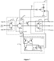
- FIG. 7 is a schematic structural diagram of a receiving apparatus in a negative voltage mode according to the present disclosure.
- FIG. 8 is a waveform diagram of the structure in FIG. 7 .
- the positive voltage mode refers to a mode in which a second high voltage signal NVDD and a second low voltage signal NGND each are a positive voltage signal all the time.
- a dual-power system includes a first power system and a second power system.
- the first power system is configured to provide a first high voltage signal VDD and a first low voltage signal GND
- the second power system is configured to provide a second high voltage signal NVDD and a second low voltage signal NGND.
- a voltage difference between the first high voltage signal VDD and the first low voltage signal GND is equal to that between the second high voltage signal NVDD and the second low voltage signal NGND.
- the dual-power system is configured to provide an output signal to the sending apparatus.
- the sending apparatus includes a first detection circuit 11 and a first transmission circuit 23 .
- the first detection circuit 11 is configured to output a detection signal Det.
- the detection signal Det indicates whether a voltage of the first low voltage signal GND is equal to that of the second low voltage signal NGND, or whether a voltage of the first high voltage signal VDD is equal to that of the second high voltage signal NVDD.
- the first transmission circuit 23 is configured to transmit an output signal of the dual-power system to an output terminal OUT of the sending apparatus or provide a first voltage to the output terminal OUT of the sending apparatus, based on the detection signal Det.
- the first voltage may be equal to the voltage of the first low voltage signal GND.
- the detection signal Det is a high level “1”, it is indicated that the voltage of the first low voltage signal GND is equal to that of the second low voltage signal NGND, or the voltage of the first high voltage signal VDD is equal to that of the second high voltage signal NVDD; and in a case that the detection signal Det is a low level “0”, it is indicated that the voltage of the first low voltage signal GND is not equal to that of the second low voltage signal NGND, or the voltage of the first high voltage signal VDD is not equal to that of the second high voltage signal NVDD.
- the output signal of the dual-power system is transmitted to the output terminal OUT of the sending apparatus.
- the first voltage is provided to the output terminal OUT of the sending apparatus.
- both the voltages of the second low voltage signal NGND and the first low voltage signal GND are 0V and are lower than that of the first high voltage signal VDD which is 3V.
- the voltage of the second low voltage signal NGND is increased to 7V, and the voltage of the second high voltage signal is increased to 10V from 3V accordingly.
- the voltage of the second low voltage signal NGND is higher than that of the first high voltage signal VDD and not equal to that of the first low voltage signal GND which is 0V.
- the first detection circuit 11 in the embodiment includes a first detection PMOS (p-type metal oxide semiconductor) transistor P 11 and a first current source I 11 .
- the source of the first detection PMOS transistor P 11 receives the first high voltage signal VDD.
- the gate of the first detection PMOS transistor P 11 receives the second low voltage signal NGND.
- the drain of the first detection PMOS transistor P 11 is connected to a first terminal of the first current source I 11 and outputs the detection signal Det.
- a second terminal of the first current source I 11 receives the first low voltage signal GND.
- the first transmission circuit 23 includes a first transmission gate 12 , a first bias PMOS transistor P 16 and a first transmission inverter 121 .
- a first control terminal of the first transmission gate 12 receives the detection signal Det.
- a second control terminal of the first transmission gate 12 is connected to an output terminal of the first transmission inverter 121 .
- An input terminal of the first transmission gate 12 receives the output signal.
- An output terminal of the first transmission gate 12 is connected to the drain of the first bias PMOS transistor P 16 .
- the gate of the first bias PMOS transistor P 16 receives the detection signal Det.
- the source of the first bias PMOS transistor P 16 receives the first high voltage signal VDD.
- the drain of the first bias PMOS transistor P 16 is connected to the output terminal OUT of the sending apparatus.
- An input terminal of the first transmission inverter 121 may directly receive the detection signal Det (not shown in the figure).
- the input terminal of the first transmission inverter 121 may also receive the detection signal Det via a first boost circuit 13 , thereby, ensuring the first transmission gate 12 to be turn on or off effectively.
- the first boost circuit 13 will be described in detail hereinafter.
- the first transmission gate 12 in the sending apparatus for a positive voltage mode may include a first transmission PMOS transistor P 12 and a first transmission NMOS (n-type metal oxide semiconductor) transistor N 12 .
- the source of the first transmission PMOS transistor P 12 is connected to the drain of the first transmission NMOS transistor N 12 and functions as the input terminal of the first transmission gate 12 .
- the drain of the first transmission PMOS transistor P 12 is connected to the source of the first transmission NMOS transistor N 12 and functions as the output terminal of the first transmission gate 12 .
- the gate of the first transmission NMOS transistor N 12 functions as the first control terminal of the first transmission gate 12
- the gate of the first transmission PMOS transistor P 12 functions as the second control terminal of the first transmission gate 12 .
- the first transmission circuit 23 may further include a first input inverter 14 and a first output inverter 15 .
- the input terminal of the first transmission gate 12 receives the output signal of the dual-power system via the first input inverter 14 .
- the output terminal of the first transmission gate 12 is connected to the drain of the first bias PMOS transistor P 16 and further connected to the output terminal OUT of the sending apparatus via the first output inverter 15 .
- the first boost circuit 13 is configured to process the detection signal Det.
- the input terminal of the first transmission inverter 121 receives a detection signal Ls which has been processed by the first boost circuit.
- the first boost circuit 13 may include a first boost PMOS transistor P 131 , a second boost PMOS transistor P 132 , a first boost NMOS transistor N 131 , a second boost NMOS transistor N 132 , a first boost inverter 131 and a second boost inverter 132 .
- Both the sources of the first boost PMOS transistor P 131 and the second boost PMOS transistor P 132 receive the second high voltage signal NVDD. Both the sources of the first boost NMOS transistor N 131 and the second boost NMOS transistor N 132 receive the first low voltage signal GND.
- the gate of the first boost PMOS transistor P 131 is connected to the drain of the second boost PMOS transistor P 132 and the drain of the second boost NMOS transistor N 132 .
- the drain of the first boost PMOS transistor P 131 is connected to the gate of the second boost PMOS transistor P 132 and the drain of the first boost NMOS transistor N 131 , and outputs the detection signal Ls which has been processed by the first boost circuit 13 .
- the gate of the first boost NMOS transistor N 131 is connected to an input terminal of the first boost inverter 131 and an output terminal of the second boost inverter 132 .
- the gate of the second boost inverter 132 is connected to an output terminal of the first boost inverter 131 .
- Both supply terminals of the first boost inverter 131 and the second boost inverter 132 receive the first high voltage signal VDD.
- An input terminal of the second boost inverter 132 receives the detection signal Det.
- the first detection PMOS transistor P 11 is turned on, and the detection signal Det outputted by the first detection circuit 11 is a high level “1” having a voltage equal to that of the first high voltage signal VDD, which indicates that the voltage of the second low voltage signal NGND is equal to that of the first low voltage signal GND.
- the detection signal Det causes the first transmission NMOS transistor N 12 in the first transmission gate 12 to be turned on, the first bias PMOS transistor P 16 to be turned off, the first boost NMOS transistor N 131 in the first boost circuit 13 to be turned off, the second boost PMOS transistor P 132 in the first boost circuit 13 to be turned off, and the second boost NMOS transistor N 132 in the first boost circuit 13 to be turned on.
- a gate voltage of the first boost PMOS transistor P 131 is equal to the voltage of the first low voltage signal GND, whereby the first boost PMOS transistor P 131 is turned on and a voltage of the detection signal Ls which has been processed by the first boost circuit 13 is equal to that of the second high voltage signal NVDD.
- the detection signal Ls which has been processed by the first boost circuit 13 causes the first transmission PMOS transistor P 12 in the first transmission gate 12 to be turned on. Since the first transmission PMOS transistor P 12 and the first transmission NMOS transistor N 12 in the first transmission gate 12 are in the on state, the first transmission gate 12 transmits the output signal of the dual-power system to the output terminal OUT of the sending apparatus.
- the first detection PMOS transistor P 11 is turned off, and the detection signal Det outputted by the first detection circuit 11 is a low level “0” having a voltage equal to that of the first low voltage signal GND, which indicates that the voltage of the second low voltage signal NGND is not equal to that of the first low voltage signal GND.
- the detection signal Det causes the first transmission NMOS transistor N 12 in the first transmission gate 12 to be turned off, the first bias PMOS transistor P 16 to be turned on, the second boost NMOS transistor N 132 in the first boost circuit to be turned off, the first boost PMOS transistor P 131 in the first boost circuit to be turned off, and the first boost NMOS transistor N 131 in the first boost circuit to be turned on.
- a voltage of the detection signal Ls which has been processed by the first boost circuit 13 is equal to that of the first low voltage signal GND.
- the detection signal Ls which has been processed by the first boost circuit 13 causes the first transmission PMOS transistor P 12 in the first transmission gate 12 to be turned off. Since the first transmission PMOS transistor P 12 and the first transmission NMOS transistor N 12 in the first transmission gate 12 are in the off state, and the first bias PMOS transistor P 16 is in the on state, a voltage of the output terminal of the first transmission gate 12 is equal to that of the first high voltage signal VDD.
- the NMOS transistor N 15 in the first output inverter 15 is turned on and the PMOS transistor P 15 in the first output inverter 15 is turned off, and the voltage of the output terminal OUT of the sending apparatus is equal to that of the first low voltage signal GND, that is, the first voltage provided by the first transmission circuit 23 is equal to the voltage of the first low voltage signal GND.
- the voltage of the second low voltage signal NGND is equal to that of the first low voltage signal GND, and a signal of the output terminal OUT of the sending apparatus is the same as the output signal of the dual-power system.
- the voltage of the second low voltage signal NGND is not equal to that of the first low voltage signal GND, and the voltage of the signal of the output terminal OUT of the sending apparatus is equal to that of the first low voltage signal GND.
- the above sending apparatus of the dual-power system may be connected to one or more receiving systems, and the one or more receiving systems each may be a single-power system. Specifically, the one or more receiving system are connected to the output terminal OUT of the sending apparatus, and a supply voltage of each of the one or more receiving systems is higher than or equal to the first voltage.
- the one or more receiving systems each may include a third power system, and the third power system is configured to provide a third high voltage signal and a third low voltage signal.
- a voltage difference between the third high voltage signal and the third low voltage signal is equal to that between the first high voltage signal VDD and the first low voltage signal GND, a voltage of the third high voltage signal is equal to that of the first high voltage signal VDD and the first voltage is equal to the voltage of the first low voltage signal GND.
- the sending apparatus plays a role of isolation, and blocks the one or more receiving systems from the dual-power system, thereby, preventing the one or more receiving systems from being damaged.
- the first detection circuit 11 may further include two inverters connected in series (which are shown but not identified in FIG. 1 ), and the detection signal is processed by the two inverters connected in series and then outputted, which may also be applied in the following embodiments and will not be described redundantly therein.
- the negative voltage mode refers to a mode in which a second high voltage signal NVDD includes a positive voltage signal and a negative voltage signal.
- a dual-power system in the embodiment is configured to provide an output signal to the sending apparatus.
- the structure of the sending apparatus for a negative voltage mode in the embodiment is similar to that of the sending apparatus for a positive voltage mode in the previous embodiment, which includes a first detection circuit 21 and a first transmission circuit 26 .
- the first detection circuit 21 is configured to output a detection signal Det.
- the detection signal Det indicates whether a voltage of the first low voltage signal GND is equal to that of the second low voltage signal NGND, or whether a voltage of the first high voltage signal VDD is equal to that of the second high voltage signal NVDD.
- the first transmission circuit 26 is configured to transmit an output signal of the dual-power system to an output terminal OUT of the sending apparatus or provide a first voltage to the output terminal OUT of the sending apparatus, based on the detection signal Det.
- the first voltage may be equal to the voltage of the first low voltage signal GND.
- the detection signal Det is a high level “1”, it is indicated that the voltage of the first low voltage signal GND is equal to that of the second low voltage signal NGND, or the voltage of the first high voltage signal VDD is equal to that of the second high voltage signal NVDD; and in a case that the detection signal Det is a low level “0”, it is indicated that the voltage of the first low voltage signal GND is not equal to that of the second low voltage signal NGND, or the voltage of the first high voltage signal VDD is not equal to that of the second high voltage signal NVDD.
- the output signal of the dual-power system is transmitted to the output terminal OUT of the sending apparatus.
- the first voltage is provided to the output terminal OUT of the sending apparatus.
- both the voltages of the second low voltage signal NGND and the first low voltage signal GND are 0V, and the voltage of the second high voltage signal NVDD which is 3V is higher than that of the first low voltage signal GND which is 0V.
- the voltage of the second low voltage signal NGND is reduced to ⁇ 5V, and is not equal to that of the first low voltage signal GND which is 0V, and correspondingly, the voltage of the second high voltage signal is reduced to ⁇ 2V from 3V.
- the voltage of the second high voltage signal NVDD which is ⁇ 2V is lower than that of the first low voltage signal GND which is 0V.
- the first detection circuit 21 in the embodiment includes a second detection NMOS transistor N 21 and a second current source I 21 .
- a first terminal of the second current source I 21 receives the first high voltage signal VDD, and a second terminal of the second current source I 21 is connected to the drain of the second detection NMOS transistor N 21 and outputs the detection signal Det.
- the gate of the second detection NMOS transistor N 21 receives the second high voltage signal NVDD, and the source of the second detection NMOS transistor N 21 receives the first low voltage signal GND.
- the first transmission circuit 26 includes a first transmission gate 22 , a first bias PMOS transistor P 26 and a first transmission inverter 221 .
- a first control terminal of the first transmission gate 22 receives the detection signal Det.
- a second control terminal of the first transmission gate 22 is connected to an output terminal of the first transmission inverter 221 .
- An input terminal of the first transmission gate 22 receives the output signal of the dual-power system.
- An output terminal of the first transmission gate 22 is connected to the drain of the first bias PMOS transistor P 26 .
- the gate of the first bias PMOS transistor P 26 receives an inversion signal of the detection signal Det. Phase inverting of the detection signal Det is performed by an inverter 222 in the embodiment.
- the source of the first bias PMOS transistor P 26 receives the first high voltage signal VDD.
- the drain of the first bias PMOS transistor P 26 is connected to the output terminal OUT of the sending apparatus.
- An input terminal of the first transmission inverter 221 receives the detection signal Det (not shown in the figure).
- the input terminal of the first transmission inverter 221 may also receive the detection signal Det via a first boost circuit 23 , thereby, ensuring the first transmission gate 22 to be turn on or off effectively.
- the first boost circuit 23 will be described in detail hereinafter.
- the first transmission gate 22 in the sending apparatus for a negative voltage mode may include a first transmission PMOS transistor P 22 and a first transmission NMOS transistor N 22 .
- the source of the first transmission PMOS transistor P 22 is connected to the drain of the first transmission NMOS transistor N 22 and functions as the input terminal of the first transmission gate 22 .
- the drain of the first transmission PMOS transistor P 22 is connected to the source of the first transmission NMOS transistor N 22 and functions as the output terminal of the first transmission gate 22 .
- the gate of the first transmission PMOS transistor P 22 functions as the first control terminal of the first transmission gate 22
- the gate of the first transmission NMOS transistor N 22 functions as the second control terminal of the first transmission gate 22 .
- the first transmission circuit 26 may further include a first input inverter 24 and a first output inverter 25 .
- the input terminal of the first transmission gate 22 receives the output signal of the dual-power system via the first input inverter 24 .
- the output terminal of the first transmission gate 22 is connected to the drain of the first bias PMOS transistor P 26 and further connected to the output terminal OUT of the sending apparatus via the first output inverter 25 .
- the first boost circuit 23 is configured to process the detection signal Det.
- the input terminal of the first transmission inverter 221 receives a detection signal Ls which has been processed by the first boost circuit 23 .
- the first boost circuit 23 may include a first boost PMOS transistor P 231 , a second boost PMOS transistor P 232 , a first boost NMOS transistor N 231 , a second boost NMOS transistor N 232 , a first boost inverter 231 and a second boost inverter 232 .
- the structure of the first boost circuit 23 is the same as that of the first boost circuit 13 in the previous embodiment, and reference can be made to FIG. 3 and the corresponding section in the previous embodiment for detailed description.
- the second detection PMOS transistor P 21 is turned off, the detection signal Det outputted by the first detection circuit 21 is a high level “1” having a voltage equal to that of the first high voltage signal VDD, which indicates that the voltage of the second low voltage signal NGND is not equal to that of the first low voltage signal GND.
- the detection signal Det causes the first transmission PMOS transistor P 22 in the first transmission gate 22 to be turned off, the first bias PMOS transistor P 26 to be turned on, the second boost NMOS transistor N 232 in the first boost circuit 23 to be turned on, the first boost PMOS transistor P 231 in the first boost circuit 23 to be turned on, the first boost NMOS transistor N 231 in the first boost circuit 23 to be turned off, and the second boost PMOS transistor P 232 in the first boost circuit 23 to be turned off.
- a voltage of the detection signal Ls which has been processed by the first boost circuit 23 is equal to that of the second high voltage signal NVDD
- the detection signal Ls which has been processed by the first boost circuit 23 causes the first transmission NMOS transistor N 22 in the first transmission gate 22 to be turned off. Since the first transmission PMOS transistor P 22 and the first transmission NMOS transistor N 22 in the first transmission gate 22 are in the off state and the first bias PMOS transistor P 26 is in the on state, a voltage of the output terminal of the first transmission gate 22 is equal to that of the first high voltage signal VDD.
- an NMOS transistor N 25 in the first output inverter 25 is turned on and a PMOS transistor P 25 in the first output inverter 25 is turned off, and the voltage of the output terminal OUT of the sending apparatus is equal to that of the first low voltage signal GND, that is, the first voltage provided by the first transmission circuit 26 is equal to the voltage of the first low voltage signal GND.
- the second detection PMOS transistor P 21 is turned on, the detection signal Det outputted by the first detection circuit 21 is a low level “0” having a voltage equal to that of the first low voltage signal GND, which indicates that the voltage of the second low voltage signal NGND is equal to that of the first low voltage signal GND.
- the detection signal Det causes the second transmission PMOS transistor P 22 in the first transmission gate 22 to be turned off, the first bias PMOS transistor P 26 to be turned off, the second boost NMOS transistor N 232 in the first boost circuit 23 to be turned off, the first boost PMOS transistor P 231 in the first boost circuit 23 to be turned off, and the first boost NMOS transistor N 231 in the first boost circuit 23 to be turned on.
- a voltage of a detection signal Ls which has been processed by the first boost circuit 23 is equal to that of the first low voltage signal GND.
- the detection signal Ls which has been processed by the first boost circuit 23 causes the first transmission NMOS transistor N 22 in the first transmission gate 22 to be turned on. Since the first transmission PMOS transistor P 22 and the first transmission NMOS transistor N 22 in the first transmission gate 22 are in the on state, the first transmission gate 22 transmits the output signal of the dual-power system to the output terminal OUT of the sending apparatus.
- the voltage of the second low voltage signal NGND is equal to that of the first low voltage signal GND, and a signal of the output terminal OUT of the sending apparatus is the same as the output signal.
- the voltage of the second low voltage signal NGND is not equal to that of the first low voltage signal GND, and a voltage of the signal of the output terminal OUT of the sending apparatus is equal to that of the first low voltage signal GND.
- the sending apparatus in the embodiment may also be connected to one or more single-power receiving systems.
- the sending apparatus in the embodiment plays a role of isolation, and blocks the one or more single-power receiving systems from the dual-power system, thereby, preventing the one or more single-power receiving systems from being damaged.
- the positive voltage mode refers to a mode in which a second high voltage signal NVDD and a second low voltage signal NGND each are a positive voltage signal all the time.
- a dual-power system in the embodiment is connected to an output terminal OUT 2 of the receiving apparatus.
- the receiving apparatus includes a second detection circuit 31 and a second transmission circuit 21 .
- the second detection circuit 31 is configured to output a detection signal Det.
- the detection signal Det indicates whether a voltage of a first low voltage signal GND is equal to that of the second low voltage signal NGND, or whether a voltage of a first high voltage signal VDD is equal to that of the second high voltage signal NVDD.
- the second transmission circuit 21 is configured to transmit an input signal of the dual-power system to the output terminal OUT 2 of the receiving apparatus or provide a second voltage to the output terminal OUT 2 of the receiving apparatus, based on the detection signal Det.
- the second voltage may be equal to the voltage of the second low voltage signal NGND.
- the detection signal Det is a high level “1”, it is indicated that the voltage of the first low voltage signal GND is equal to that of the second low voltage signal NGND, or the voltage of the first high voltage signal VDD is equal to that of the second high voltage signal NVDD; and in a case that the detection signal Det is a low level “0”, it is indicated that the voltage of the first low voltage signal GND is not equal to that of the second low voltage signal NGND, or the voltage of the first high voltage signal VDD is not equal to that of the second high voltage signal NVDD.
- the input signal is transmitted to the output terminal OUT 2 of the receiving apparatus.
- the second voltage is provided to the output terminal OUT 2 of the receiving apparatus.
- both the voltages of the second low voltage signal NGND and the first low voltage signal GND are 0V and are lower than that of the first high voltage signal VDD which is 3V.
- the voltage of the second low voltage signal NGND is increased to 5V, and correspondingly, the voltage of the second high voltage signal is increased to 8V from 3V.
- the voltage of the second low voltage signal NGND is higher than that of the first high voltage signal VDD and is not equal to that of the first low voltage signal GND which is 0V.
- the second detection circuit 31 in the embodiment includes a third detection PMOS transistor P 31 and a third current source I 31 .
- the source of the third detection PMOS transistor P 31 receives the first high voltage signal VDD.
- the gate of the third detection PMOS transistor P 31 receives the second low voltage signal NGND.
- the drain of the third detection PMOS transistor P 31 is connected to a first terminal of the third current source I 31 and outputs the detection signal Det.
- a second terminal of the third current source I 31 receives the first low voltage signal GND.
- the second transmission circuit 21 includes a second transmission gate 32 , a second bias PMOS transistor P 36 and a second transmission inverter 321 .
- a first control terminal of the second transmission gate 32 receives the detection signal Det.
- a second control terminal of the second transmission gate 32 is connected to an output terminal of the second transmission inverter 321 .
- An input terminal of the second transmission gate 32 receives the input signal.
- An output terminal of the second transmission gate 32 is connected to the drain of the second bias PMOS transistor P 36 .
- the gate of the second bias PMOS transistor P 36 receives the detection signal Det.
- the source of the second bias PMOS transistor P 36 receives the second high voltage signal NVDD.
- the drain of the second bias PMOS transistor P 36 is connected to the output terminal OUT 2 of the receiving apparatus.
- An input terminal of the second transmission inverter 321 may directly receive the detection signal Det (not shown in the figure).
- the input terminal of the second transmission inverter 321 may also receive the detection signal Det via a second boost circuit 33 , thereby, ensuring the second transmission gate 32 to be turn on or off effectively.
- the second boost circuit 33 will be described in detail hereinafter.
- the second transmission gate 32 in the receiving apparatus for a positive voltage mode may include a second transmission PMOS transistor P 32 and a second transmission NMOS transistor N 32 .
- the source of the second transmission PMOS transistor P 32 is connected to the drain of the second transmission NMOS transistor N 32 and functions as the input terminal of the second transmission gate 32 .
- the drain of the second transmission PMOS transistor P 32 is connected to the source of the second transmission NMOS transistor N 32 and functions as the output terminal of the second transmission gate 32 .
- the gate of the second transmission NMOS transistor N 32 functions as the first control terminal of the second transmission gate 32
- the gate of the second transmission PMOS transistor P 32 functions as the second control terminal of the second transmission gate 32 .
- the second transmission circuit 21 may further include a second input inverter 34 and a second output inverter 35 .
- the input terminal of the second transmission gate 32 receives the input signal of the dual-power system via the second input inverter 34 .
- the output terminal of the second transmission gate 32 is connected to the drain of the second bias PMOS transistor P 36 and further connected to the output terminal OUT 2 of the receiving apparatus via the second output inverter 35 .
- the second boost circuit 33 is configured to process the detection signal Det.
- the input terminal of the second transmission inverter 321 receives a detection signal Ls which has been processed by the second boost circuit.
- the second boost circuit 33 may include a first boost PMOS transistor P 331 , a second boost PMOS transistor P 332 , a first boost NMOS transistor N 331 , a second boost NMOS transistor N 332 , a first boost inverter 331 and a second boost inverter 332 .
- Both the sources of the first boost PMOS transistor P 331 and the second boost PMOS transistor P 332 receive the second high voltage signal NVDD. Both the sources of the first boost NMOS transistor N 331 and the second boost NMOS transistor N 332 receive the first low voltage signal GND.
- the gate of the first boost PMOS transistor P 331 is connected to the drain of the second boost PMOS transistor P 332 and the drain of the second boost NMOS transistor N 332 .
- the drain of the first boost PMOS transistor P 331 is connected to the gate of the second boost PMOS transistor P 332 and the drain of the first boost NMOS transistor N 331 , and outputs the detection signal Ls which has been processed by the second boost circuit 33 .
- the gate of the first boost NMOS transistor N 331 is connected to an input terminal of the first boost inverter 331 and an output terminal of the second boost inverter 332 .
- the gate of the second boost inverter 332 is connected to an output terminal of the first boost inverter 331 .
- Both supply terminals of the first boost inverter 331 and the second boost inverter 332 receive the first high voltage signal VDD.
- An input terminal of the second boost inverter 332 receives the detection signal Det.
- the third detection PMOS transistor P 31 is turned on, the detection signal Det outputted by the second detection circuit 31 is a high level “1” having a voltage equal to that of the first high voltage signal VDD, which indicates that the voltage of the second low voltage signal NGND is equal to that of the first low voltage signal GND.
- the detection signal Det causes the second transmission NMOS transistor N 32 in the second transmission gate 32 to be turned on, the second bias PMOS transistor P 36 to be turned off, the first boost NMOS transistor N 331 in the second boost circuit 33 to be turned off, the second boost PMOS transistor P 332 in the second boost circuit 33 to be turned off, and the second boost NMOS transistor N 332 in the second boost circuit 33 to be turned on.
- a gate voltage of the first boost PMOS transistor P 331 is equal to the voltage of the first low voltage signal GND, whereby the first boost PMOS transistor P 331 is turned on, and a voltage of the detection signal Ls which has been processed by the second boost circuit 33 is equal to that of the second high voltage signal NVDD.
- the detection signal Ls which has been processed by the second boost circuit 33 causes the second transmission PMOS transistor P 32 in the second transmission gate 32 to be turned on. Since the second transmission PMOS transistor P 32 and the second transmission NMOS transistor N 32 in the second transmission gate 32 are in the on state, the second transmission gate 32 transmits the input signal of the dual-power system to the output terminal OUT 2 of the receiving apparatus.
- the third detection PMOS transistor P 31 is turned off, and the detection signal Det outputted by the second detection circuit 31 is a low level “0” having a voltage equal to that of the first low voltage signal GND, which indicates that the voltage of the second low voltage signal NGND is not equal to that of the first low voltage signal GND.
- the detection signal Det causes the second transmission NMOS transistor N 32 in the second transmission gate 32 to be turned off, the second bias PMOS transistor P 36 to be turned on, the second boost NMOS transistor N 332 in the second boost circuit to be turned off, the first boost PMOS transistor P 331 in the second boost circuit to be turned off, and the first boost NMOS transistor N 331 in the second boost circuit to be turned on.
- a voltage of the detection signal Ls which has been processed by the second boost circuit 33 is equal to that of the first low voltage signal GND.
- the detection signal Ls which has been processed by the second boost circuit 33 causes the second transmission PMOS transistor P 32 in the second transmission gate 32 to be turned off. Since the second transmission PMOS transistor P 32 and the second transmission NMOS transistor N 32 in the second transmission gate 32 are in the off state and the second bias PMOS transistor P 36 is in the on state, a voltage of the output terminal of the second transmission gate 32 is equal to that of the second high voltage signal NVDD.
- the NMOS transistor N 35 in the second output inverter 35 is turned on and the PMOS transistor P 35 in the second output inverter 35 is turned off, and the voltage of the output terminal OUT 2 of the receiving apparatus is equal to that of the second low voltage signal NGND, that is, the second voltage provided by the second transmission circuit 21 is equal to the voltage of the second low voltage signal NGND.
- the voltage of the second low voltage signal NGND is equal to that of the first low voltage signal GND, and the signal of the output terminal OUT 2 of the receiving apparatus is the same as the input signal.
- the voltage of the second low voltage signal NGND is not equal to that of the first low voltage signal GND, and the voltage of the signal of the output terminal OUT 2 of the receiving apparatus is equal to that of the second low voltage signal NGND.
- the above receiving apparatus of the dual-power system may be connected to one or more sending systems, and the one or more sending systems each may be a single-power system.
- the one or more sending systems are configured to provide the input signal of the dual-power system.
- the one or more sending systems each may include a third power system, and the third power system is configured to provide a third high voltage signal and a third low voltage signal.
- a voltage difference between the third high voltage signal and the third low voltage signal is equal to that between the first high voltage signal VDD and the first low voltage signal GND, a voltage of the third high voltage signal is equal to that of the first high voltage signal VDD, and the second voltage is equal to that of the second low voltage signal NGND.
- the receiving apparatus in the embodiment plays a role of isolation, and blocks the one or more receiving systems from the dual-power system, thereby, preventing the one or more single-power sending systems from being damaged.
- the negative voltage mode refers to a mode in which a second high voltage signal NVDD includes a positive voltage signal and a negative voltage signal.
- a dual-power system in the embodiment is connected to an output terminal OUT 2 of the receiving apparatus.
- the structure of the receiving apparatus for a negative voltage mode in the embodiment is similar to that of the receiving apparatus for a positive voltage mode in the previous embodiment, which includes a second detection circuit 41 and a second transmission circuit 22 .
- the second detection circuit 41 is configured to output a detection signal Det.
- the detection signal Det indicates whether a voltage of the first low voltage signal GND is equal to that of the second low voltage signal NGND, or whether a voltage of the first high voltage signal VDD is equal to that of the second high voltage signal NVDD.
- the second transmission circuit 22 is configured to transmit an input signal of the dual-power system to the output terminal OUT 2 of the receiving apparatus or provide a second voltage to the output terminal OUT 2 of the receiving apparatus, based on the detection signal Det.
- the detection signal Det is a high level “1”, it is indicated that the voltage of the first low voltage signal GND is equal to that of the second low voltage signal NGND, or the voltage of the first high voltage signal VDD is equal to that of the second high voltage signal NVDD; and in a case that the detection signal Det is a low level “0”, it is indicated that the voltage of the first low voltage signal GND is not equal to that of the second low voltage signal NGND, or the voltage of the first high voltage signal VDD is not equal to that of the second high voltage signal NVDD.
- the input signal is transmitted to the output terminal OUT 2 of the receiving apparatus.
- the second voltage is provided to the output terminal OUT 2 of the receiving apparatus.
- both the voltages of the second low voltage signal NGND and the first low voltage signal GND are 0V, and the voltage of the second high voltage signal NVDD which is 3V is higher than that of the first low voltage signal GND which is 0V.
- the voltage of the second low voltage signal NGND is reduced to ⁇ 5V, which is not equal to that of the first low voltage signal GND which is 0V, and correspondingly, the voltage of the second high voltage signal is reduced to ⁇ 2V from 3V.
- the voltage of the second high voltage signal NVDD which is ⁇ 2V is lower than that of the first low voltage signal GND which is 0V.
- the second detection circuit 41 in the embodiment includes a fourth detection NMOS transistor P 41 and a fourth current source I 41 .
- a first terminal of the fourth current source I 41 receives the first high voltage signal VDD, and a second terminal of the fourth current source I 41 is connected to the drain of the fourth detection NMOS transistor P 41 and outputs the detection signal Det.
- the gate of the fourth detection NMOS transistor P 41 receives the second high voltage signal NVDD, and the source of the second detection NMOS transistor P 41 receives the first low voltage signal GND.
- the second transmission circuit 22 includes a second transmission gate 42 , a second bias PMOS transistor P 46 and a second transmission inverter 421 .
- a first control terminal of the second transmission gate 42 receives the detection signal Det.
- a second control terminal of the second transmission gate 42 is connected to an output terminal of the second transmission inverter 421 .
- An input terminal of the second transmission gate 42 receives the input signal.
- An output terminal of the transmission gate 22 is connected to the drain of the second bias PMOS transistor P 46 .
- the gate of the second bias PMOS transistor P 46 receives an inversion signal of the detection signal Det.
- an inverter 422 is configured to invert a phase of the detection signal Det.
- the source of the second bias PMOS transistor P 46 receives the second high voltage signal NVDD.
- the drain of the second bias PMOS transistor P 46 is connected to the output terminal OUT 2 of the receiving apparatus.
- An input terminal of the second transmission inverter 421 may directly receive the detection signal Det (not shown in the figure).
- the second transmission inverter 421 may also receive the detection signal Det via a second boost circuit 43 , thereby, ensuring the second transmission gate 42 to be turn on or off effectively.
- the second boost circuit 43 will be described in detail hereinafter.
- the second transmission gate 42 in the receiving apparatus for a negative voltage mode may include a second transmission PMOS transistor P 42 and a second transmission NMOS transistor N 42 .
- the source of the second transmission PMOS transistor P 42 is connected to the drain of the second transmission NMOS transistor N 42 and functions as the input terminal of the second transmission gate 42 .
- the drain of the second transmission PMOS transistor P 42 is connected to the source of the second transmission NMOS transistor N 42 and functions as the output terminal of the second transmission gate 42 .
- the gate of the second transmission PMOS transistor P 42 functions as the first control terminal of the second transmission gate 42
- the gate of the second transmission NMOS transistor N 42 functions as the second control terminal of the second transmission gate 42 .
- the second transmission circuit 22 may further include a second input inverter 44 and a second output inverter 45 .
- the input terminal of the second transmission gate 42 receives the input signal via the second input inverter 44 .
- the output terminal of the second transmission gate 42 is connected to the drain of the second bias PMOS transistor P 46 and further connected to the output terminal OUT 2 of the receiving apparatus via the second output inverter 45 .
- the second boost circuit 43 is configured to process the detection signal Det.
- the input terminal of the second transmission inverter 421 receives a detection signal Ls which has been processed by the second boost circuit 43 .
- the second boost circuit 43 may include a first boost PMOS transistor P 431 , a second boost PMOS transistor P 432 , a first boost NMOS transistor N 431 , a second boost NMOS transistor N 432 , a first boost inverter 431 and a second boost inverter 432 .
- the structure of the second boost circuit 43 is the same as that of the second boost circuit 33 in the previous embodiment, and reference can be made to FIG. 7 and the corresponding section in the previous embodiment for detailed description.
- the fourth detection PMOS transistor P 41 is turned off, and the detection signal Det outputted by the second detection circuit 41 is a high level “1” having a voltage equal to that of the first high voltage signal VDD, which indicates that the voltage of the second low voltage signal NGND is not equal to that of the first low voltage signal GND.
- the detection signal Det causes the first transmission PMOS transistor P 42 in the second transmission gate 42 to be turned off, the second bias PMOS transistor P 46 to be turned on, the second boost NMOS transistor N 432 in the second boost circuit 43 to be turned on, the first boost PMOS transistor P 431 in the second boost circuit 43 to be turned on; the first boost NMOS transistor N 431 in the second boost circuit 43 to be turned off, and the second boost NMOS transistor P 432 in the second boost circuit 43 to be turned off.
- the voltage of the detection signal Ls which has been processed by the second boost circuit 43 is equal to that of the second high voltage signal NVDD.
- the detection signal Ls which has been processed by the second boost circuit 43 causes the second transmission NMOS transistor N 42 in the second transmission gate 42 to be turned off. Since the second transmission PMOS transistor P 42 and the second transmission NMOS transistor N 42 in the second transmission gate 42 are in the off state, and the second bias PMOS transistor P 46 is in the on state, the voltage of the output terminal of the second transmission gate 42 is equal to that of the second high voltage signal NVDD.
- the NMOS transistor N 45 in the second output inverter 45 is turned on and the PMOS transistor P 45 in the second output inverter 45 is turned on, and the voltage of the output terminal OUT 2 of the receiving apparatus is equal to that of the second low voltage signal NGND, that is, the second voltage provided by the second transmission circuit 22 is equal to the voltage of the second low voltage signal NGND.
- the fourth detection PMOS transistor P 41 is turned on, and the detection signal Det outputted by the second detection circuit 41 is a low level “0” having a voltage equal to that of the first low voltage signal GND, which indicates that the voltage of the second low voltage signal NGND is equal to that of the first low voltage signal GND.
- the detection signal Det causes the second transmission PMOS transistor P 42 in the second transmission gate 42 to be turned off, the second bias PMOS transistor P 46 to be turned off, the second boost NMOS transistor N 432 in the second boost circuit 43 to be turned off, the first boost PMOS transistor P 431 in the second boost circuit 43 to be turned off, and the first boost NMOS transistor N 431 in the second boost circuit 43 to be turned on.
- a voltage of the detection signal Ls which has been processed by the second boost circuit 43 is equal to that of the first low voltage signal GND.
- the detection signal Ls which has been processed by the second boost circuit 43 causes the second transmission NMOS transistor N 42 in the second transmission gate 42 to be turned on.
- the second transmission gate 42 transmits the input signal to an input terminal IN.
- the voltage of the second low voltage signal NGND is equal to that of the first low voltage signal GND, and a signal of the output terminal OUT 2 of the receiving apparatus is the same as the input signal of the dual-power system.
- the voltage of the second low voltage signal NGND is not equal to that of the first low voltage signal GND, and a voltage of the signal of the output terminal OUT 2 of the receiving apparatus is equal to that of the second low voltage signal NGND.
- the receiving apparatus in the embodiment may also be connected to one or more single-power sending systems.
- the receiving apparatus in the embodiment plays a role of isolation, and blocks the one or more sending systems from the dual-power system, thereby, preventing the one or more sending systems from being damaged.
- a transmitting apparatus of a dual-power system is further provided according to an embodiment of the present disclosure, which includes the sending apparatus according to the above embodiments and one or more receiving systems.
- Each of the one or more receiving systems is connected to a signal output terminal of the sending apparatus, and a supply voltage of each of the one or more receiving systems is higher than or equal to the first voltage.
- Another transmitting apparatus of a dual-power system is further provided according to an embodiment of the present disclosure, which includes one or more sending systems and the receiving apparatus according to the above embodiments.
- Each of the one or more sending systems is configured to provide an input signal of the dual-power system.
- a fingerprint recognition system is further provided according to an embodiment of the present disclosure, which includes a dual-power system and the transmitting apparatus according to the above embodiment.
- the dual-power system is configured to provide an output signal of the dual-power system to the input terminal of the sending apparatus. Or, the dual-power system is connected to the output terminal of the receiving apparatus.
Landscapes
- Engineering & Computer Science (AREA)
- Physics & Mathematics (AREA)
- Computer Hardware Design (AREA)
- General Physics & Mathematics (AREA)
- Mathematical Physics (AREA)
- Computing Systems (AREA)
- General Engineering & Computer Science (AREA)
- Theoretical Computer Science (AREA)
- Power Engineering (AREA)
- Multimedia (AREA)
- Toxicology (AREA)
- Human Computer Interaction (AREA)
- Health & Medical Sciences (AREA)
- Computer Vision & Pattern Recognition (AREA)
- Computer Networks & Wireless Communication (AREA)
- Microelectronics & Electronic Packaging (AREA)
- Electromagnetism (AREA)
- Artificial Intelligence (AREA)
- General Health & Medical Sciences (AREA)
- Logic Circuits (AREA)
- Infusion, Injection, And Reservoir Apparatuses (AREA)
Abstract
Description
Claims (24)
Applications Claiming Priority (3)
| Application Number | Priority Date | Filing Date | Title |
|---|---|---|---|
| CN201610639236.9 | 2016-08-05 | ||
| CN201610639236 | 2016-08-05 | ||
| CN201610639236.9A CN107688759B (en) | 2016-08-05 | 2016-08-05 | Transmission, receiving and transmission device of dual-power system and fingerprint identification system |
Publications (2)
| Publication Number | Publication Date |
|---|---|
| US20180041211A1 US20180041211A1 (en) | 2018-02-08 |
| US10566973B2 true US10566973B2 (en) | 2020-02-18 |
Family
ID=61023054
Family Applications (1)
| Application Number | Title | Priority Date | Filing Date |
|---|---|---|---|
| US15/661,619 Active 2038-09-13 US10566973B2 (en) | 2016-08-05 | 2017-07-27 | Sending, receiving and transmitting apparatuses of dual-power system and fingerprint recognition system |
Country Status (3)
| Country | Link |
|---|---|
| US (1) | US10566973B2 (en) |
| CN (1) | CN107688759B (en) |
| TW (1) | TWI604386B (en) |
Citations (2)
| Publication number | Priority date | Publication date | Assignee | Title |
|---|---|---|---|---|
| US7049865B2 (en) * | 2004-03-05 | 2006-05-23 | Intel Corporation | Power-on detect circuit for use with multiple voltage domains |
| US20080191747A1 (en) * | 2007-02-14 | 2008-08-14 | Fujitsu Limited | Semiconductor Intergrated Circuit |
Family Cites Families (8)
| Publication number | Priority date | Publication date | Assignee | Title |
|---|---|---|---|---|
| US6909204B2 (en) * | 2003-04-01 | 2005-06-21 | Agilent Technologies, Inc. | System for sequencing a first node voltage and a second node voltage |
| JP2009022093A (en) * | 2007-07-11 | 2009-01-29 | Ricoh Co Ltd | Multi-output power supply |
| JP5169415B2 (en) * | 2008-04-11 | 2013-03-27 | 株式会社リコー | Power supply device and method for changing output voltage of power supply device |
| CN201319520Y (en) * | 2008-12-03 | 2009-09-30 | 泉州雷航电子有限公司 | Double-power intelligent switch control circuit system |
| US8724421B2 (en) * | 2012-07-18 | 2014-05-13 | Lsi Corporation | Dual rail power supply scheme for memories |
| CN103199606A (en) * | 2013-04-03 | 2013-07-10 | 华信邮电咨询设计研究院有限公司 | -48V direct current single system double-power-source device and power output control method |
| CN105515552B (en) * | 2015-12-24 | 2018-09-11 | 上海华虹宏力半导体制造有限公司 | Clock generation circuit and double power-supply system |
| CN105449839B (en) * | 2015-12-30 | 2019-01-22 | 中国能源建设集团广东省电力设计研究院有限公司 | Isolated high-speed double power-supply switching device |
-
2016
- 2016-08-05 CN CN201610639236.9A patent/CN107688759B/en active Active
- 2016-12-23 TW TW105142884A patent/TWI604386B/en active
-
2017
- 2017-07-27 US US15/661,619 patent/US10566973B2/en active Active
Patent Citations (2)
| Publication number | Priority date | Publication date | Assignee | Title |
|---|---|---|---|---|
| US7049865B2 (en) * | 2004-03-05 | 2006-05-23 | Intel Corporation | Power-on detect circuit for use with multiple voltage domains |
| US20080191747A1 (en) * | 2007-02-14 | 2008-08-14 | Fujitsu Limited | Semiconductor Intergrated Circuit |
Also Published As
| Publication number | Publication date |
|---|---|
| US20180041211A1 (en) | 2018-02-08 |
| CN107688759B (en) | 2020-07-31 |
| TW201810117A (en) | 2018-03-16 |
| TWI604386B (en) | 2017-11-01 |
| CN107688759A (en) | 2018-02-13 |
Similar Documents
| Publication | Publication Date | Title |
|---|---|---|
| US11005476B2 (en) | Level shift circuit and fingerprint identification device | |
| US11342037B2 (en) | Shift register unit, driving method, light emitting control gate driving circuit, and display apparatus | |
| CN112688708B (en) | Low power receiver circuit for isolating data communications | |
| US10811899B2 (en) | Power switching circuit | |
| US8269547B2 (en) | Bootstrap circuit | |
| US8841942B2 (en) | Voltage switch circuit | |
| US7446564B2 (en) | Level shifter | |
| US10469074B2 (en) | Power on/off reset circuit and reset signal generating circuit including the same | |
| US20160005374A1 (en) | Display driving circuit and output buffer circuit thereof | |
| US10972102B2 (en) | Interface circuit | |
| US10496224B2 (en) | Touch sensing circuit, touch panel and display device | |
| US9306571B2 (en) | Multiple voltage input buffer and related method | |
| US20110102046A1 (en) | Interfacing between differing voltage level requirements in an integrated circuit system | |
| US8130030B2 (en) | Interfacing between differing voltage level requirements in an integrated circuit system | |
| US10566973B2 (en) | Sending, receiving and transmitting apparatuses of dual-power system and fingerprint recognition system | |
| US20050012536A1 (en) | High-to-low level shifter | |
| US9571094B2 (en) | Switch circuit | |
| US10153755B2 (en) | Signal receiver, related method, and related electronic device | |
| US20110298493A1 (en) | Voltage level shift circuit and semiconductor device | |
| US10152922B2 (en) | Scan driving circuit | |
| EP3240193B1 (en) | Low core power leakage structure in io receiver during io power down | |
| US10063225B1 (en) | Voltage switching device and method | |
| US8503136B2 (en) | Protecting circuit and control circuit for reducing leakage current | |
| CN107481760B (en) | Negative voltage output circuit | |
| US9547558B2 (en) | Computer recovery circuit |
Legal Events
| Date | Code | Title | Description |
|---|---|---|---|
| AS | Assignment |
Owner name: FOCALTECH ELECTRONICS, LTD., CAYMAN ISLANDS Free format text: ASSIGNMENT OF ASSIGNORS INTEREST;ASSIGNORS:WANG, YUNN-HWA;FAM, KUET LIONG;REEL/FRAME:043119/0404 Effective date: 20161027 |
|
| STPP | Information on status: patent application and granting procedure in general |
Free format text: DOCKETED NEW CASE - READY FOR EXAMINATION |
|
| STPP | Information on status: patent application and granting procedure in general |
Free format text: NOTICE OF ALLOWANCE MAILED -- APPLICATION RECEIVED IN OFFICE OF PUBLICATIONS |
|
| STPP | Information on status: patent application and granting procedure in general |
Free format text: PUBLICATIONS -- ISSUE FEE PAYMENT RECEIVED |
|
| STCF | Information on status: patent grant |
Free format text: PATENTED CASE |
|
| AS | Assignment |
Owner name: FOCALTECH ELECTRONICS (SHENZHEN) CO., LTD., CHINA Free format text: ASSIGNMENT OF ASSIGNORS INTEREST;ASSIGNOR:FOCALTECH ELECTRONICS, LTD.;REEL/FRAME:064136/0555 Effective date: 20230509 |
|
| MAFP | Maintenance fee payment |
Free format text: PAYMENT OF MAINTENANCE FEE, 4TH YEAR, LARGE ENTITY (ORIGINAL EVENT CODE: M1551); ENTITY STATUS OF PATENT OWNER: LARGE ENTITY Year of fee payment: 4 |