US10566449B2 - Dual-operation depletion/enhancement mode high electron mobility transistor - Google Patents
Dual-operation depletion/enhancement mode high electron mobility transistor Download PDFInfo
- Publication number
- US10566449B2 US10566449B2 US15/958,579 US201815958579A US10566449B2 US 10566449 B2 US10566449 B2 US 10566449B2 US 201815958579 A US201815958579 A US 201815958579A US 10566449 B2 US10566449 B2 US 10566449B2
- Authority
- US
- United States
- Prior art keywords
- fet
- disposed
- barrier
- tct
- channel
- Prior art date
- Legal status (The legal status is an assumption and is not a legal conclusion. Google has not performed a legal analysis and makes no representation as to the accuracy of the status listed.)
- Expired - Fee Related
Links
Images


Classifications
-
- H—ELECTRICITY
- H10—SEMICONDUCTOR DEVICES; ELECTRIC SOLID-STATE DEVICES NOT OTHERWISE PROVIDED FOR
- H10D—INORGANIC ELECTRIC SEMICONDUCTOR DEVICES
- H10D30/00—Field-effect transistors [FET]
- H10D30/40—FETs having zero-dimensional [0D], one-dimensional [1D] or two-dimensional [2D] charge carrier gas channels
- H10D30/47—FETs having zero-dimensional [0D], one-dimensional [1D] or two-dimensional [2D] charge carrier gas channels having two-dimensional [2D] charge carrier gas channels, e.g. nanoribbon FETs or high electron mobility transistors [HEMT]
- H10D30/471—High electron mobility transistors [HEMT] or high hole mobility transistors [HHMT]
- H10D30/473—High electron mobility transistors [HEMT] or high hole mobility transistors [HHMT] having confinement of carriers by multiple heterojunctions, e.g. quantum well HEMT
- H10D30/4732—High electron mobility transistors [HEMT] or high hole mobility transistors [HHMT] having confinement of carriers by multiple heterojunctions, e.g. quantum well HEMT using Group III-V semiconductor material
- H10D30/4738—High electron mobility transistors [HEMT] or high hole mobility transistors [HHMT] having confinement of carriers by multiple heterojunctions, e.g. quantum well HEMT using Group III-V semiconductor material having multiple donor layers
-
- H—ELECTRICITY
- H10—SEMICONDUCTOR DEVICES; ELECTRIC SOLID-STATE DEVICES NOT OTHERWISE PROVIDED FOR
- H10D—INORGANIC ELECTRIC SEMICONDUCTOR DEVICES
- H10D30/00—Field-effect transistors [FET]
- H10D30/40—FETs having zero-dimensional [0D], one-dimensional [1D] or two-dimensional [2D] charge carrier gas channels
- H10D30/47—FETs having zero-dimensional [0D], one-dimensional [1D] or two-dimensional [2D] charge carrier gas channels having two-dimensional [2D] charge carrier gas channels, e.g. nanoribbon FETs or high electron mobility transistors [HEMT]
- H10D30/471—High electron mobility transistors [HEMT] or high hole mobility transistors [HHMT]
- H10D30/473—High electron mobility transistors [HEMT] or high hole mobility transistors [HHMT] having confinement of carriers by multiple heterojunctions, e.g. quantum well HEMT
- H10D30/4732—High electron mobility transistors [HEMT] or high hole mobility transistors [HHMT] having confinement of carriers by multiple heterojunctions, e.g. quantum well HEMT using Group III-V semiconductor material
- H10D30/4735—High electron mobility transistors [HEMT] or high hole mobility transistors [HHMT] having confinement of carriers by multiple heterojunctions, e.g. quantum well HEMT using Group III-V semiconductor material having delta-doped or planar-doped donor layers
-
- H01L29/7784—
-
- H01L27/0883—
-
- H01L29/1095—
-
- H01L29/66431—
-
- H—ELECTRICITY
- H10—SEMICONDUCTOR DEVICES; ELECTRIC SOLID-STATE DEVICES NOT OTHERWISE PROVIDED FOR
- H10D—INORGANIC ELECTRIC SEMICONDUCTOR DEVICES
- H10D30/00—Field-effect transistors [FET]
- H10D30/01—Manufacture or treatment
- H10D30/015—Manufacture or treatment of FETs having heterojunction interface channels or heterojunction gate electrodes, e.g. HEMT
-
- H—ELECTRICITY
- H10—SEMICONDUCTOR DEVICES; ELECTRIC SOLID-STATE DEVICES NOT OTHERWISE PROVIDED FOR
- H10D—INORGANIC ELECTRIC SEMICONDUCTOR DEVICES
- H10D62/00—Semiconductor bodies, or regions thereof, of devices having potential barriers
- H10D62/10—Shapes, relative sizes or dispositions of the regions of the semiconductor bodies; Shapes of the semiconductor bodies
- H10D62/17—Semiconductor regions connected to electrodes not carrying current to be rectified, amplified or switched, e.g. channel regions
- H10D62/351—Substrate regions of field-effect devices
- H10D62/357—Substrate regions of field-effect devices of FETs
-
- H—ELECTRICITY
- H10—SEMICONDUCTOR DEVICES; ELECTRIC SOLID-STATE DEVICES NOT OTHERWISE PROVIDED FOR
- H10D—INORGANIC ELECTRIC SEMICONDUCTOR DEVICES
- H10D62/00—Semiconductor bodies, or regions thereof, of devices having potential barriers
- H10D62/10—Shapes, relative sizes or dispositions of the regions of the semiconductor bodies; Shapes of the semiconductor bodies
- H10D62/17—Semiconductor regions connected to electrodes not carrying current to be rectified, amplified or switched, e.g. channel regions
- H10D62/393—Body regions of DMOS transistors or IGBTs
-
- H—ELECTRICITY
- H10—SEMICONDUCTOR DEVICES; ELECTRIC SOLID-STATE DEVICES NOT OTHERWISE PROVIDED FOR
- H10D—INORGANIC ELECTRIC SEMICONDUCTOR DEVICES
- H10D84/00—Integrated devices formed in or on semiconductor substrates that comprise only semiconducting layers, e.g. on Si wafers or on GaAs-on-Si wafers
- H10D84/80—Integrated devices formed in or on semiconductor substrates that comprise only semiconducting layers, e.g. on Si wafers or on GaAs-on-Si wafers characterised by the integration of at least one component covered by groups H10D12/00 or H10D30/00, e.g. integration of IGFETs
- H10D84/82—Integrated devices formed in or on semiconductor substrates that comprise only semiconducting layers, e.g. on Si wafers or on GaAs-on-Si wafers characterised by the integration of at least one component covered by groups H10D12/00 or H10D30/00, e.g. integration of IGFETs of only field-effect components
- H10D84/83—Integrated devices formed in or on semiconductor substrates that comprise only semiconducting layers, e.g. on Si wafers or on GaAs-on-Si wafers characterised by the integration of at least one component covered by groups H10D12/00 or H10D30/00, e.g. integration of IGFETs of only field-effect components of only insulated-gate FETs [IGFET]
- H10D84/84—Combinations of enhancement-mode IGFETs and depletion-mode IGFETs
-
- H—ELECTRICITY
- H10—SEMICONDUCTOR DEVICES; ELECTRIC SOLID-STATE DEVICES NOT OTHERWISE PROVIDED FOR
- H10D—INORGANIC ELECTRIC SEMICONDUCTOR DEVICES
- H10D84/00—Integrated devices formed in or on semiconductor substrates that comprise only semiconducting layers, e.g. on Si wafers or on GaAs-on-Si wafers
- H10D84/80—Integrated devices formed in or on semiconductor substrates that comprise only semiconducting layers, e.g. on Si wafers or on GaAs-on-Si wafers characterised by the integration of at least one component covered by groups H10D12/00 or H10D30/00, e.g. integration of IGFETs
- H10D84/82—Integrated devices formed in or on semiconductor substrates that comprise only semiconducting layers, e.g. on Si wafers or on GaAs-on-Si wafers characterised by the integration of at least one component covered by groups H10D12/00 or H10D30/00, e.g. integration of IGFETs of only field-effect components
Definitions
- the present disclosure relates to transistors and in particular to a dual-operation depletion/enhancement mode high electron mobility transistor.
- FETs Field-effect transistors
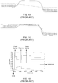
- FIG. 1 a when operating a FET 10 , a voltage applied to a terminal 12 called the “Gate Electrode” acts on mobile charge carriers remotely through a front barrier 14 which may be insulating, weakly conducting, or semiconducting. The mobile charge carriers get pulled into/depleted from a “channel” region 16 , by means of electrostatic fields.
- the gate electrode 12 may form or disrupt a conductive “bridge” in the channel region 16 between two other terminals 18 , 20 called the “Source Electrode” and the “Drain Electrode”, respectively, depending on: (a) the voltage magnitude and voltage polarity applied externally to the gate electrode 12 ; (b) the polarity of charge being pulled into, or depleted from, the channel 16 by the gate 12 (negative for electrons, positive for electron vacancies also known as “holes”); and (c) the polarity and quantity of immobile fixed charges either present in the channel 16 or in the front barrier 14 .
- Other structures of the FET 10 may include a conducting cap 22 disposed on the front barrier 14 , which in turn is disposed on the channel 16 .
- the channel 16 may be disposed on a back barrier 24 , which in turn is disposed on a substrate 26 .
- a pulse doping layer 28 may be disposed within the front barrier 14 , with the pulse doping layer 28 being, for example, an n++ or donor of electrons traveling from the source 18 to the drain 20 .
- D-Mode depletion-mode
- E-Mode enhancement-mode
- FIG. 1 a A high-electron mobility transistor (HEMT) in the prior art is illustrated in FIG. 1 a , which is a FET in which the front barrier 14 is a semiconductor as well, usually an alloy different in elemental composition from the material of the channel 14 .
- the front barrier 14 With a semiconducting front barrier 14 , it is easier in practice to insert fixed electrical charges that would further modulate the response of electrons in the channel 16 to the gate voltage.
- FIG. 1 a A variant of the basic HEMT structure in the prior art, shown as the FET 30 in FIG.
- band energy diagram is the energy of the edge of the conduction band (CB) pictured as a function of spatial position.
- the band energy diagrams such as shown in FIG. 1 d , are constructed such that, under the prevalent electrostatic fields, electrons tend to pool near the bottom of the profile.
- the dashed lines show the “chemical potential” (also known as Fermi level) which may be considered an energy reference for the CB. It is important to note that the lower the CB energy relative to this reference at any point, the larger the electron concentration at that point.
- FIG. 1 d shows the band energy diagram in a vertical section through the center of FIG. 1 a , cutting through the gate metal, front barrier, channel, back barrier and substrate.
- the barriers are made of a semiconductor of a different material or alloy composition than the channel.
- An example plot of material elemental composition vs. vertical location is illustrated in FIG. 1 e .
- a conduction band “well” forms at the barrier-channel interface, where electrons can be made to pool by increasing the gate voltage, as explained below. This pool of electrons, once created by applying a large enough gate voltage, would bridge the source and drain terminals and allow an electrical current.
- FIGS. 1 b -1 c show schematically the CB energy as a function of position in the channel, across the device of FIG. 1 a from source to drain terminals.
- the gate voltage is very low, the CB energy in the channel under the gate electrode is high, presenting a potential step that blocks electrons from transferring from source to drain, even if the drain CB energy is lower than that of the source.
- the step height decreases, until a threshold gate voltage is reached.
- this threshold voltage also known as “pinch-off voltage”
- electrons in the source can gain enough energy from random thermal excitations to overcome the step, as shown in FIG. 1 c , after which they are accelerated by the drain voltage into the drain terminal, providing current at the drain terminal.
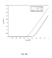
- FIG. 3 a -3 b display exemplary plots of the drain current I D versus the gate-to-source voltage V GS .
- the source is chosen to be the zero of potential throughout the present disclosure.
- a fixed positive voltage is applied to the drain to collect the electrons launched from the source. This drain voltage is often close to the highest DC voltage in the system, such as the positive power supply rail.
- a threshold voltage is present during which the drain current is small, followed by an abrupt increase as the potential step becomes low enough to be surmounted by electrons thermally excited from the source. Beyond this point, the current at the drain monotonically increases as the increasing gate voltage attracts more and more electrons into the channel.
- FIG. 3 a represents a D-Mode FET, since the threshold voltage for conduction to begin is negative
- FIG. 3 b represents an E-Mode FET, since the threshold voltage is positive.
- the other terminal as a “fourth terminal”, considered in the prior art typically belongs to a different device on the same chip, causing nominally isolated devices on the same chip to become electrically coupled. This coupling is through (a) direct current injection by the fourth terminal, (b) indirect modulation of the channel potential through charging or discharging interface traps beneath the channel, or (c) direct electrostatic modulation of the channel potential.
- back-gating or “side-gating” in the prior art, such as in Boroumand et al., “Observations of Backgate Impedance Dispersion in GaAs Isolation Structures”, IEEE TRANSACTIONS ON ELECTRON DEVICES, Vol. 48, No. 9, September 2011, pp. 1850-1858; Kocot et al., “Backgating in GaAs MESFET's”, IEEE TRANSACTIONS ON MICROWAVE THEORY AND TECHNIQUES, Vol. MTT-30, No. 7, July 1982, pp.
- n-doped (donor-doped) layer has been utilized as an investigative tool to examine charge-potential characteristics of free GaAs surfaces, as described in the prior art such as Kawaharazuka et al., “Study of Free GaAs Surfaces Using a Back-gated Undoped GaAs/AlGaAs Heterostructure, PHYSICA E, Vol. 13, 2002, pp. 663-666.
- the Kawaharazuka reference (a) describes essentially a 3-terminal device viewed upside-down, and (b) serves a different purpose to that in the present inventive disclosure.
- n-doped layers if attempted to be used as threshold-control terminal (TCT) access layers, are incompatible with dual E/D-Mode operation with a single power supply. This is because E-mode operation in such a hypothetical device would need a negative voltage applied to the n-doped layer.
- TCT threshold-control terminal
- the present invention is a FET having a p-doped (acceptor-doped) layer underneath a FET channel to enable E/D Mode operation.
- a FET threshold voltage is tunable through a voltage applied to the p-doped layer via a metal contact such as a threshold-control terminal (TCT).
- TCT threshold-control terminal
- the present invention has a dual E/D mode operation of a single FET device, and also a dual E/D mode operation with a single-polarity positive power supply voltage.
- the FET of the present invention is fabricated to enable dual enhancement-mode/depletion-mode (E-Mode/D-Mode) high electron mobility transistors (HEMTs), to enable dual E/D Mode operation by incorporating a p-doped (acceptor doped) region underneath the channel, to achieve tunable threshold voltage by varying the bias voltage on a fourth terminal called the threshold-control terminal (TCT) that contacts the p-doped layer, and to enable Dual E/D-Mode operation of a HEMT with a single-polarity positive power supply voltage.
- E-Mode/D-Mode high electron mobility transistors
- the present invention includes a field-effect transistor (FET) comprising: a substrate; a back barrier disposed on the substrate; a middle barrier disposed above the back barrier, wherein at least one pulse-doping layer is disposed within the middle barrier; a channel disposed on the middle barrier; and a front barrier disposed on the channel.
- a threshold-control terminal (TCT) access layer is disposed between the middle barrier and the back barrier, wherein a voltage applied to the TCT access layer tunes a threshold voltage of the FET.
- a front hole-blocker layer is disposed between the middle barrier and the TCT access layer.
- a spacer layer is disposed between the middle barrier and the TCT access layer.
- a back hole-blocker layer is disposed between the back barrier and the TCT access layer.
- a spacer layer is disposed between the back barrier and the TCT access layer.
- the front barrier includes at least one pulse-doping layer disposed therein.
- a substrate contact is included upon which the substrate is disposed.
- an n-doped threshold-control terminal (TCT) access layer is disposed between the middle barrier and the back barrier, wherein a voltage applied to the TCT access layer tunes the threshold voltage of the FET.
- the carriers of electrical current in the FET channel are electron-holes.
- the channel is doped, which acts as a bridge between the source and the drain.
- a source terminal and a drain terminal are included, wherein the bridge is disrupted by “depleting” the channel through the application of a voltage opposite in polarity to that of the ionized impurities functioning as the dopants of the doped channel.
- the FET is selected from a hetero-junction FET (HFET), a junction gate FET (JFET), and a metal-semiconductor FET (MESFET).
- a p-doped threshold-control terminal (TCT) access layer, a spacer layer, and a hole-blocking layer are included, wherein at least one of the p-doped TCT access layer, the spacer layer, the hole-blocking layer, the channel, the front barrier, the middle barrier, and the back barrier is composed of a compound selected from (In)GaAs, (In)GaP, (Ga)AlAs, (Al)InAs, (In)GaN or (Ga)AlN.
- the substrate is composed of a compound selected from GaAs, InP, GaN, Si, SiC or Al2O 3 .
- the present invention includes a field-effect transistor (FET) comprising: a substrate; a back barrier disposed on the substrate; a threshold-control terminal (TCT) access layer disposed above the back barrier, wherein a voltage applied to the TCT access layer tunes a threshold voltage of the FET; a middle barrier disposed above the TCT access layer, wherein at least one pulse-doping layer is disposed within the middle barrier; a channel disposed on the middle barrier; a front barrier disposed on the channel; and a gate disposed on the front barrier.
- the TCT access layer is p-doped.
- a TCT contact is disposed on the TCT access layer.
- the present invention includes a method for fabricating a field-effect transistor (FET) comprising: providing a substrate; disposing a back barrier on the substrate; disposing a threshold-control terminal (TCT) access layer above the back barrier; disposing a middle barrier above the TCT access layer; disposing at least one pulse-doping layer within the middle barrier; disposing a channel on the middle barrier; disposing a front barrier on the channel; and applying a voltage to the TCT access layer, thereby tuning a threshold voltage of the FET.
- FET field-effect transistor
- FIG. 1 a illustrates a FET in the prior art
- FIGS. 1 b -1 c illustrate conduction band profiles across the FET of FIG. 1 a;
- FIG. 1 d illustrates a conduction band profile through the center of the FET of FIG. 1 a;
- FIG. 1 e illustrates a material composition profile through the center of the FET of FIG. 1 a
- FIG. 2 illustrates a FET with front and back barriers with pulse doping
- FIG. 3 a illustrates an I D vs. V GS chart for a depletion-mode HEMT
- FIG. 3 b illustrates an I D vs. V GS chart for an enhancement-mode HEMT
- FIG. 4 illustrates an FET of the present invention having a middle barrier
- FIG. 5 a illustrates an HEMT of the present invention with a mesa
- FIG. 5 b illustrates a variant of the HEMT of FIG. 5 a
- FIG. 6 a illustrates an energy band diagram of the FET of FIG. 4 ;
- FIG. 6 b illustrates a chart of a dual D/E-Mode operation of the FET of FIG. 4 .
- the present invention is a HEMT 40 with a TCT-contacting p-doped layer 42 .
- a gate 44 is disposed on a front barrier 46 , which in turn is disposed on a channel 48 .
- the channel 48 is disposed on a middle barrier 50 , which is disposed on the p-doped layer 42 .
- the p-doped layer 42 is disposed on a back barrier 52 , which in turn is disposed on a substrate 54 .
- the middle barrier 50 includes at least one pulse doping layer 56 , 58 .
- the front barrier 46 may optionally include a pulse doping layer 60 .
- An optional front hole-blocker 62 and/or an optional first undoped spacer 64 may be included between the middle barrier 50 and the TCT-contacting p-doped layer 42 .
- an optional back hole-blocker 66 and/or an optional second undoped spacer 68 may be included between the TCT-contacting p-doped layer 42 and the back barrier 52 .
- a substrate contact 70 may optionally be included under the substrate 54 .
- the back barrier 52 may optionally be pulse-doped, which will further reduce hole injection into the substrate 54 . If the TCT-access layer 42 is p-doped, then the pulse-doped back barrier 52 is n-doped. Alternatively, if the TCT-access layer 42 is n-doped, then the pulse-doped back barrier 52 is p-doped.
- the front barrier 46 is composed of AlGaAs
- the channel 48 is composed of (In)GaAs
- the middle barrier 50 is composed of AlGaAs
- the optional front hole-blocker 62 is composed of AlAs
- the optional first undoped spacer 64 is composed of (In)GaAs
- the TCT-access p-doped layer 42 is also composed of (In)GaAs
- the optional second spacer 68 is also composed of (In)GaAs
- the optional back hole-blocker 66 is composed of AlAs
- the back barrier 52 is composed of AlGaAs
- the substrate 54 is composed of GaAs.
- FIG. 6 a shows the conduction band energy diagram with 1 volt on the TCT in the top diagram, and 0 volt on the TCT in the bottom diagram for the HEMT 40 in FIG. 4 .
- the channel 48 is kept at 0 volt.
- the p-doped layer 42 would be between about 20 nm and about 2 microns in thickness, and is disposed on the substrate 54 . With 0 volt on the TCT, it is seen that the p-doped layer 42 (which is depleted of holes resulting in a net fixed, immobile negative charge) pulls the conduction band in the channel up and away from the Fermi level of the TCT, as in the bottom diagram in FIG. 6 a .
- the p-doped layer 42 gets less depleted of holes, resulting in too few negative immobile charges to sustain sufficient repulsion of channel electrons.
- the conduction band-edge in the channel 48 gets pulled down towards and below the Fermi level. This causes the electron concentration in the channel 48 to increase, thus enabling the channel 48 to serve as a conductive path from source to drain.
- just 0 volt on the gate is enough to turn the device “ON”; in other words, the FET 40 operates in D-Mode.
- FIG. 6 b shows the I D vs V GS characteristics of the FET 40 at 0 volt and 1 volt on the TCT, showing a clear transition from E-Mode to D-Mode operation.
- the operation of the TCT is not discrete, or “digital”, and so the TCT voltage can be continuously tuned to achieve the desired threshold voltage of the FET 40 , be it strongly E-Mode, be it strongly D-Mode, or be it somewhere in-between, as dictated by the needs of the application circuit.
- the example FET 40 is fabricated in order to prevent hole injection from the p-doped layer 42 , by surrounding the layer 42 on both sides by AlGaAs barriers as the middle barrier 50 and the back barrier 52 .
- TCT voltages may be achieved by using a wide band-gap material such as AlAs on either side of the p-doped channel 48 , which offers an even larger barrier, for example, up to about 2 eV, for holes to surmount if the holes are to cross over into the valence bands of adjacent layers.
- These “hole-blocking” layers 62 , 66 shown in FIG. 4 on either side of the p-doped layer 42 would range in thickness from about 2 nm to about 20 nm.
- Additional undoped spacers 64 , 68 around the p-doped region, as shown in FIG. 4 may be used to further tailor the threshold voltage as a function of TCT voltage, and to provide etch-stops for easier fabrication of TCT contacts.
- FIGS. 5 a -5 b shows schematics of alternative devices 80 , 90 , respectively, fabricated based on the structure of FIG. 4 , with the p-doped region 42 contacted by a metal to form TCT contacts 82 , 92 , respectively. Standard photolithography, wet or dry chemical etching, and/or metallization processes may be used to form these TCT contacts 82 , 92 .
- FIG. 5 a illustrates a FET 80 which features a TCT contact 82 fabricated on a separate mesa 84 for each individual device 86 .
- FIG. 5 b illustrates a FET 90 which features a universal TCT contact 92 for all devices 94 , 96 , 98 combined.
- inventive devices 80 , 90 in FIGS. 5 a -5 b may be expected to yield a threshold voltage tunable between about ⁇ 2 to about +2 volt, using about 0 to about +10 volt applied to the TCT contacts 82 , 92 , respectively.
- the threshold voltage is tunable between a lower value ranging from about ⁇ 0.5 to about ⁇ 0.1 volt, and an upper value ranging from about +0.1 to about +0.7 volt, using about 0 to about +1 volt applied to the TCT contacts 82 , 92 . This would enable dual E/D Mode operation on a single FET with a single-polarity (positive-only) power supply.
- the present invention includes different flavors of FETs apart from HEMTs.
- counter-doped layers are disposed underneath the channel that modify the threshold voltage in hole-channel (p-channel) FETs when the carriers of electrical current are holes rather than electrons.
- the TCT access layer would then be n-doped.
- doped TCT-access layers are disposed underneath the channel that enable tunability of the threshold voltage in FETs that deplete a doped channel, i.e. a pre-existing bridge between the source and drain, by applying a voltage opposite in polarity to the ionized impurities (dopants).
- dopants include Hetero-Junction FETs (HFET), a junction gate FET (JFET) and Metal-Semiconductor FETs (MESFETs).
- FIG. 46 may have a uniformly doped layer in the place of any pulse-doping layer, with the uniformly doped layer having the same polarity as the pulse-doping layer which is replaced.
- the front barrier 46 includes an n-doped pulse-doping layer, such an n-doped pulse-doping layer 60
- the pulse-doping layer 60 may be replaced with an n-doped uniformly doped layer.
Landscapes
- Junction Field-Effect Transistors (AREA)
Abstract
Description
Claims (18)
Priority Applications (2)
| Application Number | Priority Date | Filing Date | Title |
|---|---|---|---|
| US15/958,579 US10566449B2 (en) | 2018-04-20 | 2018-04-20 | Dual-operation depletion/enhancement mode high electron mobility transistor |
| US15/979,988 US10347738B1 (en) | 2018-04-20 | 2018-05-15 | Fabrication of a dual-operation depletion/enhancement mode high electron mobility transistor |
Applications Claiming Priority (1)
| Application Number | Priority Date | Filing Date | Title |
|---|---|---|---|
| US15/958,579 US10566449B2 (en) | 2018-04-20 | 2018-04-20 | Dual-operation depletion/enhancement mode high electron mobility transistor |
Related Child Applications (1)
| Application Number | Title | Priority Date | Filing Date |
|---|---|---|---|
| US15/979,988 Continuation-In-Part US10347738B1 (en) | 2018-04-20 | 2018-05-15 | Fabrication of a dual-operation depletion/enhancement mode high electron mobility transistor |
Publications (2)
| Publication Number | Publication Date |
|---|---|
| US20190326425A1 US20190326425A1 (en) | 2019-10-24 |
| US10566449B2 true US10566449B2 (en) | 2020-02-18 |
Family
ID=68237070
Family Applications (1)
| Application Number | Title | Priority Date | Filing Date |
|---|---|---|---|
| US15/958,579 Expired - Fee Related US10566449B2 (en) | 2018-04-20 | 2018-04-20 | Dual-operation depletion/enhancement mode high electron mobility transistor |
Country Status (1)
| Country | Link |
|---|---|
| US (1) | US10566449B2 (en) |
Cited By (1)
| Publication number | Priority date | Publication date | Assignee | Title |
|---|---|---|---|---|
| US20220029007A1 (en) * | 2020-07-24 | 2022-01-27 | Vanguard International Semiconductor Corporation | Semiconductor structure and semiconductor device |
Families Citing this family (5)
| Publication number | Priority date | Publication date | Assignee | Title |
|---|---|---|---|---|
| US10971616B2 (en) * | 2018-10-31 | 2021-04-06 | Taiwan Semiconductor Manufacturing Co., Ltd. | Apparatus and circuits with dual threshold voltage transistors and methods of fabricating the same |
| US11189719B2 (en) * | 2018-10-31 | 2021-11-30 | Taiwan Semiconductor Manufacturing Co., Ltd. | Apparatus and circuits including transistors with different gate stack materials and methods of fabricating the same |
| US11024626B2 (en) * | 2018-10-31 | 2021-06-01 | Taiwan Semiconductor Manufacturing Co., Ltd. | Apparatus and circuits including transistors with different threshold voltages and methods of fabricating the same |
| WO2020129186A1 (en) * | 2018-12-19 | 2020-06-25 | 三菱電機株式会社 | Semiconductor device |
| CN112259605B (en) * | 2020-10-22 | 2022-08-23 | 东南大学 | Heterojunction semiconductor device resistant to instantaneous current impact |
Citations (1)
| Publication number | Priority date | Publication date | Assignee | Title |
|---|---|---|---|---|
| US20010002706A1 (en) * | 1997-09-12 | 2001-06-07 | Ichiro Hase | Semiconductor device |
-
2018
- 2018-04-20 US US15/958,579 patent/US10566449B2/en not_active Expired - Fee Related
Patent Citations (1)
| Publication number | Priority date | Publication date | Assignee | Title |
|---|---|---|---|---|
| US20010002706A1 (en) * | 1997-09-12 | 2001-06-07 | Ichiro Hase | Semiconductor device |
Non-Patent Citations (9)
| Title |
|---|
| Abey et al., "A Single Supply High Performance PA MMIC for GSM Handsets using Quasi-Enhancement Mode PHEMT", IEEE MTT-S Digest, 2001, pp. 923-926. |
| Bayruns et al., "The Bootstrapped Gate FET (BGFET)-A New Control Transistor", GaAs IC Symposium, 1995, pp. 136-139. |
| Bayruns et al., "The Bootstrapped Gate FET (BGFET)—A New Control Transistor", GaAs IC Symposium, 1995, pp. 136-139. |
| Boroumand et al., "Observations of Backgate Impedance Dispersion in GaAs Isolation Structures", IEEE Transactions on Electron Devices, vol. 48, No. 9, Sep. 2011, pp. 1850-1858. |
| Chen et al., "Reduction of Sidegating in GaAs Analog and Digital Circuits Using a New Buffer Layer", IEEE Transactions on Electron Devices, vol. 36, No. 9, Sep. 1989, pp. 1546-1556. |
| Kawaharazuka et al., Study of Free GaAs Surfaces Using a Back-gated Undoped GaAs/AlGaAs Heterostructure, Physica E, vol. 13, 2002, pp. 663-666. |
| Kocot et al., "Backgating in GaAs Mesfet's", IEEE Transactions on Microwave Theory and Techniques, vol. MTT-30, No. 7, Jul. 1982, pp. 963-968. |
| Lin et al., "A Delta-Doped InGaP/InGaAs PHEMT with Different Doping Profiles for Device-Linearity Improvement", IEEE Transactions on Electron Devices, vol. 54, No. 7, Jul. 2007, pp. 1617-1625. |
| Norman Fadhil Idham et al., "Device Characteristics of HEMT Structures Based on Backgate Contact Method", ICSE2006 Proc. 2006, pp. 740-742. |
Cited By (2)
| Publication number | Priority date | Publication date | Assignee | Title |
|---|---|---|---|---|
| US20220029007A1 (en) * | 2020-07-24 | 2022-01-27 | Vanguard International Semiconductor Corporation | Semiconductor structure and semiconductor device |
| US12176430B2 (en) * | 2020-07-24 | 2024-12-24 | Vanguard International Semiconductor Corporation | Semiconductor structure and semiconductor device |
Also Published As
| Publication number | Publication date |
|---|---|
| US20190326425A1 (en) | 2019-10-24 |
Similar Documents
| Publication | Publication Date | Title |
|---|---|---|
| US10566449B2 (en) | Dual-operation depletion/enhancement mode high electron mobility transistor | |
| US6555851B2 (en) | High electron mobility transistor | |
| CN101359686B (en) | Reliable normally-off III-nitride active device structure and related methods and systems | |
| US7655962B2 (en) | Enhancement mode insulated gate heterostructure field-effect transistor with electrically isolated RF-enhanced source contact | |
| US20130032860A1 (en) | HFET with low access resistance | |
| Shinohara et al. | GaN-based field-effect transistors with laterally gated two-dimensional electron gas | |
| US10170613B2 (en) | Semiconductor device | |
| US8067788B2 (en) | Semiconductor device | |
| US6479843B2 (en) | Single supply HFET with temperature compensation | |
| US20030155578A1 (en) | Heterostructure with rear-face donor doping | |
| Lour et al. | Improved breakdown in LP-MOCVD grown n+-GaAs/δ (p+)-GaInP/n-GaAs heterojunction camel-gate FET | |
| Bergman et al. | InAs/AlSb HFETs with f/sub/spl tau//and f/sub max/above 150 GHz for low-power MMICs | |
| US4652896A (en) | Modulation doped GaAs/AlGaAs field effect transistor | |
| Kohno et al. | Modeling and suppression of the surface trap effect on drain current frequency dispersions in GaAs MESFETs | |
| Leuther et al. | Metamorphic 50 nm InAs-channel HEMT | |
| Lour et al. | Comparisons between mesa-and airbridge-gate AlGaAs/InGaAs doped-channel field-effect transistors | |
| US10347738B1 (en) | Fabrication of a dual-operation depletion/enhancement mode high electron mobility transistor | |
| JP4913324B2 (en) | Field effect transistor | |
| Swain et al. | Comparative study of AlN/GaN HEMT and MOSHEMT structures by varying oxide thickness | |
| JP2000286428A (en) | Field-effect transistor | |
| Lu | Ultrawide Bandgap Nitride Semiconductor Heterojunction Field Effect Transistors | |
| US4593300A (en) | Folded logic gate | |
| KR20070104375A (en) | Monolithic Integrated Circuit with Field Effect Transistor | |
| Prost et al. | High speed, high gain InP-based heterostructure FETs with high breakdown voltage and low leakage | |
| JP2553673B2 (en) | Field effect transistor |
Legal Events
| Date | Code | Title | Description |
|---|---|---|---|
| FEPP | Fee payment procedure |
Free format text: ENTITY STATUS SET TO UNDISCOUNTED (ORIGINAL EVENT CODE: BIG.); ENTITY STATUS OF PATENT OWNER: SMALL ENTITY |
|
| FEPP | Fee payment procedure |
Free format text: ENTITY STATUS SET TO SMALL (ORIGINAL EVENT CODE: SMAL); ENTITY STATUS OF PATENT OWNER: SMALL ENTITY |
|
| AS | Assignment |
Owner name: DUET MICROELECTRONICS, INC., NEW JERSEY Free format text: CONVERSION;ASSIGNOR:DUET MICROELECTRONICS LLC;REEL/FRAME:046779/0296 Effective date: 20180701 |
|
| AS | Assignment |
Owner name: DUET MICROELECTRONICS INC., NEW JERSEY Free format text: NUNC PRO TUNC ASSIGNMENT;ASSIGNORS:BAYRUNS, JOHN;BAYRUNS, ROBERT J.;RAMU, ASHOK T.;SIGNING DATES FROM 20191212 TO 20191217;REEL/FRAME:051322/0688 |
|
| AS | Assignment |
Owner name: DUET MICROELECTRONICS INC., NEW JERSEY Free format text: NUNC PRO TUNC ASSIGNMENT;ASSIGNORS:BAYRUNS, JOHN;BAYRUNS, ROBERT J.;RAMU, ASHOK T.;SIGNING DATES FROM 20191219 TO 20191220;REEL/FRAME:051366/0177 |
|
| STPP | Information on status: patent application and granting procedure in general |
Free format text: PUBLICATIONS -- ISSUE FEE PAYMENT RECEIVED |
|
| AS | Assignment |
Owner name: DUET MICROELECTRONICS LLC, NEW JERSEY Free format text: NUNC PRO TUNC ASSIGNMENT;ASSIGNORS:BAYRUNS, JOHN;BAYRUNS, ROBERT J.;RAMU, ASHOK T.;SIGNING DATES FROM 20191219 TO 20191220;REEL/FRAME:051419/0737 |
|
| STCF | Information on status: patent grant |
Free format text: PATENTED CASE |
|
| AS | Assignment |
Owner name: XG MICROELECTRONICS INC., NEW JERSEY Free format text: ASSIGNMENT OF ASSIGNORS INTEREST;ASSIGNOR:DUET MICROELECTRONICS INC.;REEL/FRAME:052529/0323 Effective date: 20200107 |
|
| FEPP | Fee payment procedure |
Free format text: MAINTENANCE FEE REMINDER MAILED (ORIGINAL EVENT CODE: REM.); ENTITY STATUS OF PATENT OWNER: SMALL ENTITY |
|
| LAPS | Lapse for failure to pay maintenance fees |
Free format text: PATENT EXPIRED FOR FAILURE TO PAY MAINTENANCE FEES (ORIGINAL EVENT CODE: EXP.); ENTITY STATUS OF PATENT OWNER: SMALL ENTITY |
|
| STCH | Information on status: patent discontinuation |
Free format text: PATENT EXPIRED DUE TO NONPAYMENT OF MAINTENANCE FEES UNDER 37 CFR 1.362 |
|
| FP | Lapsed due to failure to pay maintenance fee |
Effective date: 20240218 |