US10566291B2 - Mark structure for aligning layers of integrated circuit structure and methods of forming same - Google Patents
Mark structure for aligning layers of integrated circuit structure and methods of forming same Download PDFInfo
- Publication number
- US10566291B2 US10566291B2 US15/898,606 US201815898606A US10566291B2 US 10566291 B2 US10566291 B2 US 10566291B2 US 201815898606 A US201815898606 A US 201815898606A US 10566291 B2 US10566291 B2 US 10566291B2
- Authority
- US
- United States
- Prior art keywords
- dielectric layer
- trenches
- marking
- marking trenches
- positioned above
- Prior art date
- Legal status (The legal status is an assumption and is not a legal conclusion. Google has not performed a legal analysis and makes no representation as to the accuracy of the status listed.)
- Expired - Fee Related
Links
Images


Classifications
-
- H01L23/544—
-
- H—ELECTRICITY
- H10—SEMICONDUCTOR DEVICES; ELECTRIC SOLID-STATE DEVICES NOT OTHERWISE PROVIDED FOR
- H10W—GENERIC PACKAGES, INTERCONNECTIONS, CONNECTORS OR OTHER CONSTRUCTIONAL DETAILS OF DEVICES COVERED BY CLASS H10
- H10W46/00—Marks applied to devices, e.g. for alignment or identification
-
- G—PHYSICS
- G01—MEASURING; TESTING
- G01N—INVESTIGATING OR ANALYSING MATERIALS BY DETERMINING THEIR CHEMICAL OR PHYSICAL PROPERTIES
- G01N21/00—Investigating or analysing materials by the use of optical means, i.e. using sub-millimetre waves, infrared, visible or ultraviolet light
- G01N21/84—Systems specially adapted for particular applications
- G01N21/88—Investigating the presence of flaws or contamination
- G01N21/95—Investigating the presence of flaws or contamination characterised by the material or shape of the object to be examined
- G01N21/9501—Semiconductor wafers
-
- G—PHYSICS
- G03—PHOTOGRAPHY; CINEMATOGRAPHY; ANALOGOUS TECHNIQUES USING WAVES OTHER THAN OPTICAL WAVES; ELECTROGRAPHY; HOLOGRAPHY
- G03F—PHOTOMECHANICAL PRODUCTION OF TEXTURED OR PATTERNED SURFACES, e.g. FOR PRINTING, FOR PROCESSING OF SEMICONDUCTOR DEVICES; MATERIALS THEREFOR; ORIGINALS THEREFOR; APPARATUS SPECIALLY ADAPTED THEREFOR
- G03F7/00—Photomechanical, e.g. photolithographic, production of textured or patterned surfaces, e.g. printing surfaces; Materials therefor, e.g. comprising photoresists; Apparatus specially adapted therefor
- G03F7/70—Microphotolithographic exposure; Apparatus therefor
- G03F7/70425—Imaging strategies, e.g. for increasing throughput or resolution, printing product fields larger than the image field or compensating lithography- or non-lithography errors, e.g. proximity correction, mix-and-match, stitching or double patterning
- G03F7/70466—Multiple exposures, e.g. combination of fine and coarse exposures, double patterning or multiple exposures for printing a single feature
-
- G—PHYSICS
- G03—PHOTOGRAPHY; CINEMATOGRAPHY; ANALOGOUS TECHNIQUES USING WAVES OTHER THAN OPTICAL WAVES; ELECTROGRAPHY; HOLOGRAPHY
- G03F—PHOTOMECHANICAL PRODUCTION OF TEXTURED OR PATTERNED SURFACES, e.g. FOR PRINTING, FOR PROCESSING OF SEMICONDUCTOR DEVICES; MATERIALS THEREFOR; ORIGINALS THEREFOR; APPARATUS SPECIALLY ADAPTED THEREFOR
- G03F7/00—Photomechanical, e.g. photolithographic, production of textured or patterned surfaces, e.g. printing surfaces; Materials therefor, e.g. comprising photoresists; Apparatus specially adapted therefor
- G03F7/70—Microphotolithographic exposure; Apparatus therefor
- G03F7/70483—Information management; Active and passive control; Testing; Wafer monitoring, e.g. pattern monitoring
- G03F7/70605—Workpiece metrology
- G03F7/70616—Monitoring the printed patterns
- G03F7/70633—Overlay, i.e. relative alignment between patterns printed by separate exposures in different layers, or in the same layer in multiple exposures or stitching
-
- G—PHYSICS
- G03—PHOTOGRAPHY; CINEMATOGRAPHY; ANALOGOUS TECHNIQUES USING WAVES OTHER THAN OPTICAL WAVES; ELECTROGRAPHY; HOLOGRAPHY
- G03F—PHOTOMECHANICAL PRODUCTION OF TEXTURED OR PATTERNED SURFACES, e.g. FOR PRINTING, FOR PROCESSING OF SEMICONDUCTOR DEVICES; MATERIALS THEREFOR; ORIGINALS THEREFOR; APPARATUS SPECIALLY ADAPTED THEREFOR
- G03F9/00—Registration or positioning of originals, masks, frames, photographic sheets or textured or patterned surfaces, e.g. automatically
- G03F9/70—Registration or positioning of originals, masks, frames, photographic sheets or textured or patterned surfaces, e.g. automatically for microlithography
- G03F9/7073—Alignment marks and their environment
- G03F9/7076—Mark details, e.g. phase grating mark, temporary mark
-
- G—PHYSICS
- G03—PHOTOGRAPHY; CINEMATOGRAPHY; ANALOGOUS TECHNIQUES USING WAVES OTHER THAN OPTICAL WAVES; ELECTROGRAPHY; HOLOGRAPHY
- G03F—PHOTOMECHANICAL PRODUCTION OF TEXTURED OR PATTERNED SURFACES, e.g. FOR PRINTING, FOR PROCESSING OF SEMICONDUCTOR DEVICES; MATERIALS THEREFOR; ORIGINALS THEREFOR; APPARATUS SPECIALLY ADAPTED THEREFOR
- G03F9/00—Registration or positioning of originals, masks, frames, photographic sheets or textured or patterned surfaces, e.g. automatically
- G03F9/70—Registration or positioning of originals, masks, frames, photographic sheets or textured or patterned surfaces, e.g. automatically for microlithography
- G03F9/7073—Alignment marks and their environment
- G03F9/7084—Position of mark on substrate, i.e. position in (x, y, z) of mark, e.g. buried or resist covered mark, mark on rearside, at the substrate edge, in the circuit area, latent image mark, marks in plural levels
-
- H01L22/12—
-
- H—ELECTRICITY
- H10—SEMICONDUCTOR DEVICES; ELECTRIC SOLID-STATE DEVICES NOT OTHERWISE PROVIDED FOR
- H10P—GENERIC PROCESSES OR APPARATUS FOR THE MANUFACTURE OR TREATMENT OF DEVICES COVERED BY CLASS H10
- H10P74/00—Testing or measuring during manufacture or treatment of wafers, substrates or devices
- H10P74/20—Testing or measuring during manufacture or treatment of wafers, substrates or devices characterised by the properties tested or measured, e.g. structural or electrical properties
- H10P74/203—Structural properties, e.g. testing or measuring thicknesses, line widths, warpage, bond strengths or physical defects
-
- H—ELECTRICITY
- H10—SEMICONDUCTOR DEVICES; ELECTRIC SOLID-STATE DEVICES NOT OTHERWISE PROVIDED FOR
- H10W—GENERIC PACKAGES, INTERCONNECTIONS, CONNECTORS OR OTHER CONSTRUCTIONAL DETAILS OF DEVICES COVERED BY CLASS H10
- H10W46/00—Marks applied to devices, e.g. for alignment or identification
- H10W46/301—Marks applied to devices, e.g. for alignment or identification for alignment
-
- H—ELECTRICITY
- H10—SEMICONDUCTOR DEVICES; ELECTRIC SOLID-STATE DEVICES NOT OTHERWISE PROVIDED FOR
- H10W—GENERIC PACKAGES, INTERCONNECTIONS, CONNECTORS OR OTHER CONSTRUCTIONAL DETAILS OF DEVICES COVERED BY CLASS H10
- H10W46/00—Marks applied to devices, e.g. for alignment or identification
- H10W46/501—Marks applied to devices, e.g. for alignment or identification for use before dicing
Definitions
- the present disclosure relates to structures formed in an integrated circuit (IC) structure to align multiple vertical layers with each other, particularly in IC structures formed with multiple patterning techniques. More particularly, the present disclosure relates to a mark structure for aligning layers of an integrated circuit (IC) structure, and methods of forming the same.
- IC integrated circuit
- Integrated circuit fabrication requires forming large numbers of interconnected devices, such as transistors, resistors, capacitors, and diodes on the surface of a semiconductor substrate material. These devices are formed in part by selectively depositing and removing multiple layers of material, e.g., semiconductors, insulators, photoresists, masks, etch stop layers, and metals. The functionality and reliability of a particular IC depends at least partially on accurate vertical alignment between each of the layers. In some cases, a fabricator may use multiple patterning lithography to place some elements in closer lateral proximity with each other than may otherwise be possible through conventional manufacturing techniques.
- Double patterning lithography is one type of multiple patterning lithography technology that has been in use for some time.
- Double patterning lithography generally involves creating shapes, e.g., one or more conductive elements for providing functional features and/or electrical connections within a device, that are within the same design layer but too close to each other to be assigned to the same mask layer.
- the shapes are instead assigned onto two different mask layers in order to satisfy spacing requirements specified in the design of the product. These two different mask layers are then used to create one layer of the IC.
- Other multiple patterning lithography options such as triple patterning lithography may use more than two masks. Accurate alignment between the multiple mask layers is therefore one of several important factors in fabrication of functional and reliable ICs.
- Accurate alignment between mask layers may be accomplished by several approaches.
- One of these approaches includes forming one or more marking structures, such as one or more overlay marks and/or one or more alignment marks in various layers of the IC as it is being processed.
- a fabricator may detect the location of a marking structure in each layer to determine whether multiple layers are aligned with each other. In the event that the detected marking structure in previously-formed layer is not in its anticipated position, the fabricator may adjust the relative position of the partially fabricated IC and the current mask reticle to bring the prior mask layer and the current mask reticle into proper alignment with one another before printing the next layer.
- marking structures may be measured by a stand-alone or in-situ metrology tool to quantify the alignment of the current layer, imaged in photoresist, relative to the prior layer etched into the substrate, to detect if misaligned features are present.
- This overlay mark metrology data then allows a determination to be made to continue fabrication, conduct rework operations and feedback offsets, or discard a defective IC.
- Typical marking structures may include several linear metal-filled trenches arranged parallel to one another within a dielectric material.
- the trenches may be arranged in groups where trenches within a group are in close proximity to one another, and multiple groups are arranged to form a structure for use as an overlay mark or alignment mark.
- the metal in these trenches is electrically isolated from the various devices, such as transistors, and may not have any function in the finished IC.
- Marking structures may optionally be positioned in kerf lines between individual dies on the semiconductor substrate.
- the effectiveness of a marking structure is at least partially dependent on the contrast between the materials and the background material of the partially fabricated IC. Higher contrast can improve the accuracy of imaging of the marking structure and thus the accuracy of final alignment between the various layers in an IC.
- Conventional methods of forming marking structures may produce marking trenches with a metal fill that is not thick enough to produce good contrast against the background when imaged. Conventional methods may also produce marking trenches that lack uniformity. Weak contrast or non-uniformity can cause unreliable results when measuring alignment, resulting in defective product or leading to expensive and time-consuming re-work operations.
- a first aspect of this disclosure is directed to a structure for alignment of an integrated circuit (IC) structure, the structure including: a first dielectric layer positioned above a semiconductor substrate, the semiconductor substrate having one or more active devices thereon; a trench stop layer positioned above the first dielectric layer; a second dielectric layer positioned above the trench stop layer; and a plurality of metal-filled marking trenches extending vertically through the second dielectric layer and the trench stop layer, and at least partially into the first dielectric layer, wherein each of the plurality of metal-filled marking trenches includes a metal electrically isolated from the one or more active devices by at least the first dielectric layer.
- IC integrated circuit
- a second aspect of this disclosure is directed to a method of forming a structure for alignment of an integrated circuit (IC) structure, the method including: forming a via hard mask on a precursor structure, wherein the precursor structure includes a semiconductor substrate, a first dielectric layer positioned above the semiconductor substrate, a trench stop layer positioned above the first dielectric layer, a second dielectric layer positioned above the trench stop layer, a first hard mask positioned above the second dielectric layer and including a plurality of preformed openings therein, a plurality of substantially parallel trench spacers positioned above the first hard mask between the plurality of preformed openings, a spin-on hard mask positioned over and between the plurality of trench spacers, and a via stop layer positioned above the spin-on hard mask; forming a plurality of first openings within the via hard mask wherein the plurality of first openings are either substantially perpendicular to the plurality of trench spacers or substantially parallel to the plurality of trench spacers, and wherein the plurality of first openings are
- a third aspect of this disclosure is directed to a method of forming a structure for alignment of an integrated circuit (IC) structure, the method including: forming a via hard mask on a precursor structure, wherein the precursor structure includes a semiconductor substrate, a first dielectric layer positioned above the semiconductor substrate, a trench stop layer positioned above the first dielectric layer, a second dielectric layer positioned above the trench stop layer, a first hard mask positioned above the second dielectric layer, a spin-on hard mask positioned above the first hard mask, and a via stop layer positioned above the spin-on hard mask, wherein the first hard mask has a plurality of preformed openings through the first hard mask; forming a plurality of first openings within the via hard mask wherein the plurality of first openings are either substantially perpendicular to the plurality of preformed openings through the first hard mask or substantially parallel to the plurality of preformed openings through the first hard mask, and wherein the plurality of first openings are positioned above the plurality of preformed openings through the first hard
- FIG. 1 shows a plan view of a precursor structure of an integrated circuit (IC) to be processed according to embodiments of this disclosure.
- FIG. 2 shows a lateral cross section view along the line 2 - 2 in FIG. 1 of the precursor structure according to embodiments of this disclosure.
- FIG. 3 shows a plan view of the IC after undergoing a first patterning operation according to embodiments of this disclosure.
- FIG. 4 shows a lateral cross section view along line 4 - 4 in FIG. 3 of the IC after undergoing a first patterning operation according to embodiments of this disclosure.
- FIG. 5 shows a plan view of the IC after undergoing a second patterning operation according to embodiments of this disclosure.
- FIG. 6 shows a lateral cross section view along line 6 - 6 in FIG. 5 of the IC after undergoing a second patterning operation according to embodiments of this disclosure.
- FIG. 7 shows a plan view of the IC after undergoing a first removal operation according to embodiments of this disclosure.
- FIG. 8 shows a lateral cross section view along line 8 - 8 in FIG. 7 of the IC after undergoing a first removal operation according to embodiments of this disclosure.
- FIG. 9 shows a plan view of the IC after undergoing a second removal operation according to embodiments of this disclosure.
- FIG. 10 shows a lateral cross section view along line 10 - 10 in FIG. 9 of the IC after undergoing a second removal operation according to embodiments of this disclosure.
- FIG. 11 shows a plan view of the IC after undergoing forming a metal in the trenches according to embodiments of this disclosure.
- FIG. 12 shows a lateral cross section view along line 12 - 12 in FIG. 11 of the IC after undergoing forming of a metal according to embodiments of this disclosure.
- FIG. 13 shows a plan view of another precursor structure of an integrated circuit (IC) to be processed according to embodiments of this disclosure.
- FIG. 14 shows a lateral cross section view along the line 14 - 14 in FIG. 13 of the precursor structure according to embodiments of this disclosure
- FIG. 15 shows a plan view of the IC after undergoing a first patterning operation according to embodiments of this disclosure.
- FIG. 16 shows a lateral cross section view along line 16 - 16 in FIG. 15 of the IC after undergoing a first patterning operation according to embodiments of this disclosure.
- FIG. 17 shows a plan view of the IC after undergoing a second patterning operation according to embodiments of this disclosure.
- FIG. 18 shows a lateral cross section view along line 18 - 18 in FIG. 17 of the IC after undergoing a second patterning operation according to embodiments of this disclosure.
- FIG. 19 shows a plan view of the IC after undergoing a first removal operation according to embodiments of this disclosure.
- FIG. 20 shows a lateral cross section view along line 20 - 20 in FIG. 19 of the IC after undergoing a first removal operation according to embodiments of this disclosure.
- FIG. 21 shows a plan view of the IC after undergoing a second removal operation according to embodiments of this disclosure.
- FIG. 22 shows a lateral cross section view along line 22 - 22 in FIG. 21 of the IC after undergoing a second removal operation according to embodiments of this disclosure.
- FIG. 23 shows a plan view of the IC after undergoing forming a metal in the trenches according to embodiments of this disclosure.
- FIG. 24 shows a lateral cross section view along line 24 - 24 in FIG. 23 of the IC after undergoing forming a metal according to embodiments of this disclosure.
- FIG. 25 shows a plan view of the IC after undergoing planarization according to embodiments of this disclosure.
- FIG. 26 shows a lateral cross section view along line 26 - 26 in FIG. 25 of the IC after undergoing planarization according to embodiments of this disclosure.
- FIG. 27 shows a plan view of one embodiment of a structure according to embodiments of this disclosure.
- FIG. 28 shows a plan view of additional embodiments of a structure according to embodiments of this disclosure.
- This disclosure relates to integrated circuit (IC) structures and fabrication techniques. More particularly, the present disclosure relates to alignment structures, alternatively “structures” hereafter, which may be used as an overlay mark, alignment mark, etc., for an IC structure.
- Integrated circuits are manufactured employing, among other operations, multiple processing steps that selectively add or remove material in one or more layers formed on a semiconductor substrate. Certain processing steps may entail multiple addition or removal operations on the same layer. Alternatively or additionally, multiple layers may be affected by a single operation or series of operations. Fabrication of functional and reliable ICs depends at least partially on accurate alignment between each of these layers and between each of the operations performed upon the layers.
- fabrication steps disclosed in this disclosure may be combined with fabrication steps performed for other purposes.
- photolithography or etching steps performed according to embodiments of this disclosure may simultaneously form other structures of the IC, including but not limited to wiring, silicon through vias, or other interconnections.
- Embodiments of the present disclosure include providing a precursor structure 100 of an integrated circuit (IC) to be processed according to one aspect of this disclosure.
- structures and methods according to the disclosure may feature a structure for aligning various layers of an IC, in which metal is formed within deeper marking trenches as compared to conventional alignment structures.
- the use of deeper marking trenches with thicker metal fill may improve imaging contrast and provide greater tolerance of non-uniformity. These improvements can increase the accuracy of alignment during fabrication, increasing yield and decreasing costs.
- FIG. 1 provides a plan view of an example precursor structure 100
- FIG. 2 provides a cross-sectional view in plane X-Z of the same structure.
- Embodiments of precursor structure 100 may contain one or more active devices or partially fabricated active devices (not shown, but typically on or in substrate 105 ) located in regions separate from the region to be used for fabrication of the marking trenches and overlay mark described in this disclosure.
- Precursor structure 100 may include multiple layers fabricated during previous processing steps.
- precursor structure 100 may include a semiconductor substrate 105 , a first dielectric layer 110 , a trench stop layer 115 , a second dielectric layer 120 , a first hard mask 125 , several trench spacers 130 positioned on first hard mask 125 , a plurality of preformed openings 138 within first hard mask 125 and laterally between trench spacers 130 , a spin-on hard-mask 140 , a via stop layer 145 , and a via hard mask 150 .
- Trench spacers 130 may be positioned within spin-on hard mask 140 and adjacent to preformed openings 135 in an alternating manner on first hard mask 125 .
- Each trench spacer 130 may include one or more currently known or later developed spacer materials suitable for integrated circuit processing, examples of which are provided herein.
- trench spacers 130 may be omitted based on the processing techniques used to form substrate 105 and layers 110 , 114 , 120 , 125 (e.g., as shown in FIG. 14 and discussed in further detail below).
- Trench spacers 130 , and/or openings where applicable may be substantially linear and extend substantially in parallel to one another. Spacing between pairs of trench spacers 130 , and/or openings in alternative embodiments, may be substantially the same or may be different in different portions of precursor structure 100 . Likewise, the width of trench spacers 130 may be substantially the same or may be different in different portions of precursor structure 100 .
- the various components of precursor structure 100 are discussed herein in more detail, with reference to FIGS. 1 and 2 , to aid in the description of subsequent processing and/or resulting structures.
- semiconductor substrate 105 may take the form of a semiconductor-on-insulator (SOI) layer.
- SOI layer typically refers to a layered silicon-insulator-silicon substrate in place of a more conventional silicon substrate (bulk substrate) in semiconductor manufacturing, especially microelectronics.
- SOI-based devices differ from conventional bulk semiconductor devices in that the semiconductor junction is above an electrical insulator, typically silicon dioxide or (less commonly) sapphire. The precise thickness of the insulating layer and topmost semiconductor layer also vary widely with the intended application.
- Dielectric materials of first dielectric layer 110 and second dielectric layer 120 may include any interlevel or intralevel dielectric material including inorganic dielectric materials, organic dielectric materials, or combinations thereof.
- First dielectric layer 120 or second dielectric layer 120 may also include additional sublayers, such as glue layers or cap layers as known in the art.
- First dielectric layer 120 may be the layer known in the art as the “zero via dielectric layer.”
- Dielectric materials may have various dielectric constants (K). High-K dielectrics, i.e., those having a dielectric constant above approximately 3.9, are employed when high capacitance is desired. Conversely, low-K and ultra-low-K dielectrics, i.e., materials having a dielectric constant of at most approximately 3.9, are employed when low capacitance is desired.
- Suitable dielectric materials include but are not limited to: carbon-doped silicon dioxide materials; fluorinated silicate glass (FSG); organic polymeric thermoset materials; silicon oxycarbide; SiCOH dielectrics; fluorine doped silicon oxide; spin-on glasses; silsesquioxanes, including hydrogen silsesquioxane (HSQ), methyl silsesquioxane (MSQ) and mixtures or copolymers of HSQ and MSQ; benzocyclobutene (BCB)-based polymer dielectrics, and any silicon-containing low-k dielectric.
- FSG fluorinated silicate glass
- organic polymeric thermoset materials silicon oxycarbide
- SiCOH dielectrics fluorine doped silicon oxide
- spin-on glasses silsesquioxanes, including hydrogen silsesquioxane (HSQ), methyl silsesquioxane (MSQ) and mixtures or copolymers of HSQ and MSQ
- spin-on low-k films with SiCOH-type composition using silsesquioxane chemistry examples include HOSPTM (available from Honeywell), JSR 5109 and 5108 (available from Japan Synthetic Rubber), ZirkonTM (available from Shipley Microelectronics, a division of Rohm and Haas), and porous low-k (ELk) materials (available from Applied Materials).
- HOSPTM available from Honeywell
- JSR 5109 and 5108 available from Japan Synthetic Rubber
- ZirkonTM available from Shipley Microelectronics, a division of Rohm and Haas
- porous low-k (ELk) materials available from Applied Materials
- carbon-doped silicon dioxide materials, or organosilanes examples include Black DiamondTM (available from Applied Materials) and CoralTM (available from Lam Research).
- An example of an HSQ material is FOxTM (available from Dow Corning).
- First hard mask 125 and via hard mask 150 of precursor structure 100 each refer to a layer of material which is applied over an underlying layer of material. After processing the underlying layer, the mask may be removed.
- An example of a commonly used hard mask material is Si 3 N 4 (“nitride”).
- Trench stop layer 115 and via stop layer 145 each refer to a layer of material which prevents damage to the underlying semiconductor or metal material during etching of layers above the stop layer. Etch stop materials feature drastically different etch characteristics than the material to be etched; a layer of etch stop material is placed underneath material to be etched to stop the etching process.
- Spin-on hard-mask 140 may be formed by one or more spin-on techniques for applying materials, which generally involves providing a stream of material to the substrate, while the substrate is spinning, resulting in a relatively thin, flat, evenly-distributed coating of the material on the underlying substrate.
- Trench spacers 130 refer to etch-resistant materials which define the boundaries between adjacent trenches formed within precursor structure 100 by subsequent etching operations.
- Trench spacers 130 may be formed from any material known to the art, such as titanium oxide (TiO2) and/or silicon oxide (SiO 2 ).
- the trench spacers 130 may be formed using a self-aligned double patterning (SADP) process, also known as sidewall image transfer (SIT) processing.
- SADP self-aligned double patterning
- SIT sidewall image transfer
- the arrangement of trench spacers 130 , or openings in alternative embodiments, will determine the arrangement of marking trenches formed during later processing steps according to embodiments of this disclosure.
- Trench spacers 130 in various embodiments may have a spacing in the range of between approximately 5 nanometers (nm) to approximately 100 nm.
- Embodiments of precursor structure 100 , and/or other precursor structures discussed herein, may be positioned laterally adjacent to one or more active devices or partially fabricated active devices (not shown, on or in substrate 105 ). Such devices may be located in regions separate from the region to be used for fabrication of the marking trenches and structure for use as an overlay or alignment mark described in this disclosure. Additionally or alternatively, precursor structure 100 and/or other precursor structures discussed herein may be formed in regions targeted for removal in subsequent processing steps, such as but not limited to kerf regions in an IC wafer. In various embodiments, one or more active devices may be formed in regions separate from the region to be used for fabrication of the alignment structure by subsequent processing steps.
- FIG. 3 provides a plan view of a partially processed structure 200 with openings 205 therein, while FIG. 4 provides a cross-sectional view in plane X-Z of the same structure.
- Processing according to embodiments of this disclosure includes using photolithography to form multiple openings 205 through via hard mask 150 positioned above trench spacers 130 . These openings may be oriented substantially perpendicular to trench spacers 130 or may be oriented substantially parallel with trench spacers 130 . The width of the openings that may be reliably created by a single photolithography step is limited due to limitations of the photolithography process and due to an etch loading effect.
- the width of the openings 205 is limited to a predetermined size depending on the specific photolithography process used. Strips 210 of via hard mask material remain over trench spacers 130 after the first photolithography step above.
- a radiation sensitive “resist” coating is formed over one or more layers which are to be treated, in some manner, such as to be selectively doped and/or to have a pattern transferred thereto.
- the resist which is sometimes referred to as a photoresist, is itself first patterned by exposing it to radiation, where the radiation (selectively) passes through an intervening mask or template containing the pattern. As a result, the exposed or unexposed areas of the resist coating become more or less soluble, depending on the type of photoresist used. A developer is then used to remove the more soluble areas of the resist leaving a patterned resist.
- the patterned resist can then serve as a mask for the underlying layers which can then be selectively treated, such as to receive dopants and/or to undergo etching, for example.
- the depth of the marking trenches formed by subsequent etching processes is limited when portions of via hard mask 150 remain above trench spacers 130 .
- Conventional methodologies that allowed residual via hard mask above the trench spacers resulted in marking trenches that penetrated only into second dielectric 120 .
- the resulting structure may exhibit poor contrast and high variation between different regions of the IC.
- residual via hard mask material will be removed by multiple pattern lithography, including a second photolithography step according to embodiments of this disclosure, as described below.
- Each pattern printed in sequence is often identified in the art as being a different “color”, although the significance of the colors is only to identify different patterns, and does not reflect actual colors.
- FIG. 5 provides a plan view of a partially processed structure 200 with an expanded opening 215 therein
- FIG. 6 provides a cross-sectional view in plane X-Z of the same structure.
- Processing according to embodiments of this disclosure includes a second photolithography step, using a second “color” mask, to form an expanded opening 215 through via hard mask 150 .
- This expanded opening 215 is positioned above trench spacers 130 , by removing the strips 210 of via hard mask 150 that remained between openings 205 after the first photolithography step.
- the second lithography step removes substantially all of via hard mask 150 above trench spacers 130 .
- FIG. 7 provides a plan view of a partially processed structure 200 with partially formed marking trenches 305 therein
- FIG. 8 provides a cross-sectional view in plane X-Z of the same structure.
- Processing according to embodiments of this disclosure includes removing via hard mask 150 , via stop layer 145 , and spin-on hard mask 140 such as by using one or more etching methods now known to the art or developed in the future. While conventional processing would typically only etch as far vertically into the IC structure as first hard mask 125 , expanded opening 215 allows etching to continue to deeper layers. Portions of first hard mask 125 and second dielectric 120 may be removed underneath expanded opening 215 where not protected by trench spacers 130 , forming partial marking trenches 305 between trench spacers 130 .
- Etching generally refers to the removal of material from a substrate (or structures formed on the substrate), and is often performed with a mask in place so that material may selectively be removed from certain areas of the substrate, while leaving the material unaffected, in other areas of the substrate.
- etching There are generally two categories of etching, (i) wet etch and (ii) dry etch.
- Wet etch is performed with a solvent (such as an acid) which may be chosen for its ability to selectively dissolve a given material (such as oxide), while leaving another material (such as polysilicon) relatively intact. This ability to selectively etch given materials is fundamental to many semiconductor fabrication processes.
- a wet etch will generally etch a homogeneous material (e.g., oxide) isotropically, but a wet etch may also etch single-crystal materials (e.g. silicon wafers) anisotropically.
- Dry etch may be performed using a plasma.
- Plasma systems can operate in several modes by adjusting the parameters of the plasma. Ordinary plasma etching produces energetic free radicals, neutrally charged, that react at the surface of the wafer. Since neutral particles attack the wafer from all angles, this process is isotropic. Ion milling, or sputter etching, bombards the wafer with energetic ions of noble gases which approach the wafer approximately from one direction, and therefore this process is highly anisotropic.
- Reactive-ion etching RIE operates under conditions intermediate between sputter and plasma etching and may be used to produce deep, narrow features, such as trenches.
- FIG. 9 provides a plan view of a partially processed structure 200 with full-depth marking trenches 310 therein, while FIG. 10 provides a cross-sectional view in plane X-Z of the same structure.
- Processing according to embodiments of this disclosure includes removing portions of second dielectric layer 120 , trench stop layer 115 , and first dielectric layer 110 , such as by using one or more etching methods now known to the art or developed in the future.
- the partial trenches 305 formed in the first etching step are extended deeper into the IC by the second etching step, breaking through trench stop layer 115 and extending at least partially into first dielectric layer 110 .
- the resulting full-depth trenches 310 may be positioned between trench spacers 130 .
- FIG. 11 provides a plan view of a partially processed structure 200 with metal deposited therein
- FIG. 12 provides a cross-sectional view in plane X-Z of the same structure.
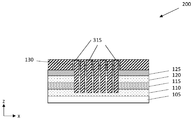
- Processing according to embodiments of this disclosure includes depositing a metal 315 in the full-depth trenches 310 .
- metal 315 is only show in full-depth trenches 310 , metal may be deposited on other portions of the IC not shown for clarity. In any case, metal 315 formed in the full-depth trenches 310 according to embodiments of this disclosure may be electrically isolated from any active devices which are also present.
- Metal 315 deposited in the full-depth marking trenches 310 can be in the form of any currently known or later developed conductive material such as, e.g., aluminum (Al), zinc (Zn), indium (In), copper (Cu), indium copper (InCu), tin (Sn), tantalum (Ta), tantalum nitride (TaN), tantalum carbide (TaC), titanium (Ti), titanium nitride (TiN), titanium carbide (TiC), tungsten (W), tungsten nitride (WN), tungsten carbide (WC), cobalt (Co), ruthenium (Ru), and/or polysilicon (poly-Si) or combinations thereof.
- metal 315 may be deposited within full-depth trenches 310 concurrently with other metal deposition techniques to form other conductive elements of an IC structure.
- metal wires, vias, etc. may be formed on laterally distal regions (not shown) of the device structure through damascene or other procedures for filling an opening in a layer with a conductive metal.
- metal 315 may be formed to at least the height of any remaining trench spacers 130 .
- the prior formation of full-depth trenches 310 may allow full-depth trenches 310 to be filled with metal 315 concurrently with other openings in an IC structure.
- precursor structure 180 shown in FIGS. 13,14 may include substantially the same components as precursor structure 100 shown in FIGS. 1,2 , but may have additional or alternative structural features.
- precursor structure 180 may be formed by way of a processes other than SADP (self-aligned double patterning). As shown in FIG. 14 , forming precursor structure 180 without SADP may yield a series of preformed openings 182 extending at least partially into first hard mask 125 , and without trench spacers 130 ( FIGS. 1-12 ). As shown, an upper surface of second dielectric layer 120 may be located at the bottom of one or more openings 182 .
- the remaining components of precursor structure 180 may be the same as those in precursor structure 100 .
- precursor structure 180 may include one or more structural differences as compared to precursor structure 100
- the embodiments of the processes described herein relative to FIGS. 1-12 may be suitable to form an IC structure 300 ( FIGS. 25-28 , discussed below) for alignment of different layers in a device. It is therefore emphasized that the processes discussed herein and shown in the accompanying FIGS. 13-24 reflect a similar or identical set of processing concepts with possible variances in implementation, discussed herein, to be performed on alternative precursor structure 180 .
- Precursor structure 180 may be processed into partially-processed structure(s) 280 ( FIGS. 15-24 ) using the same or similar processes discussed herein relative to precursor structure 100 ( FIGS. 1, 2 ) and partially-processed structure(s) 200 ( FIGS. 3-12 ). Except where noted otherwise herein, the various processing operations, materials, etc., discussed relative to FIGS. 1-12 may also be used for operations on precursor structure 180 and partially processed structure(s) 280 .
- FIGS. 15 and 16 illustrate forming openings 205 in via hard mask 150 .
- FIGS. 17 and 18 demonstrate forming expanded openings 215 in via hard mask 150 , e.g., by using a second color mask to increase the size of the previously formed openings in hard mask 205 .
- Applying a second lithography step may remove substantially all of via hard mask 150 preformed openings 182 .
- Continued manufacture as shown in FIGS. 18 and 19 may include, e.g., forming marking trenches 305 by removing via hard mask 150 , via stop layer 145 , and spin-on hard mask 140 . Portions of first hard mask 125 and second dielectric 120 may be removed beneath expanded opening 215 , forming partial marking trenches 305 .
- processing may continue by etching partial marking trenches 305 to yield full-depth marking trenches 310 therein, but without trench spacers 130 being present on first hard mask 125 .
- Partially-processed structure 280 then may be planarized such that first hard mask 125 has a horizontally planar upper surface.
- FIGS. 23 and 24 illustrate forming metal 315 on partially-processed structure 280 .
- the processes of forming metal 315 e.g., deposition, on partially-processed structure 280 may be the same as those discussed elsewhere herein relative to forming metal 315 on partially processed structure 200 , and shown in FIGS. 11 and 12 .
- the absence of trench spacers 130 in partially-processed structure 280 may cause metal 315 to be formed on, and entirely cover, first hard mask 125 .
- This may be the case in still further embodiments or precursor structures, e.g., where metal is non-selectively deposited outside full-depth marking trenches 310 .
- metal 315 may then be planarized to the upper surface of first hard mask 125 such that metal 315 is only positioned within full-depth marking trenches 310 .
- the subsequent planarizing of metal 315 may also remove any remaining trench spacers 130 .
- FIGS. 25 and 26 processes for forming finished marking trenches 315 and the corresponding IC structure 300 according to the disclosure are shown. It is noted that FIGS. 25 and 26 may represent continued processing of partially-processed structure 200 ( FIGS. 3-12 ), partially-processed structure 280 ( FIGS. 14-26 ), or other materials formed by the processing of other precursor structures.
- FIG. 25 provides a plan view of IC structure 300 with planarized metal-filled marking trenches 315 therein, while FIG. 26 provides a cross-sectional view in plane X-Z of the same structure. Processing according to this step of embodiments of this disclosure includes planarization.
- Planarization may remove trench spacers 130 , first hard mask 125 , portions of second dielectric 125 , and portions of metal 315 . After planarization, the upper surface of the metal will be substantially co-planar with the upper surface of second dielectric layer 120 .
- Planarization refers to various processes that make a surface more planar (that is, more flat and/or smooth).
- Chemical-mechanical-polishing is one currently conventional planarization process which planarizes surfaces with a combination of chemical reactions and mechanical forces.
- CMP uses slurry including abrasive and corrosive chemical components along with a polishing pad and retaining ring, typically of a greater diameter than the wafer.
- the pad and wafer are pressed together by a dynamic polishing head and held in place by a plastic retaining ring.
- the dynamic polishing head is rotated with different axes of rotation (that is, not concentric). This process removes material and tends to even out any “topography,” making the wafer flat and planar.
- planarization techniques may include: (i) oxidation; (ii) chemical etching; (iii) taper control by ion implant damage; (iv) deposition of films of low-melting point glass; (v) resputtering of deposited films to smooth them out; (vi) photosensitive polyimide (PSPI) films; (vii) new resins; (viii) low-viscosity liquid epoxies; (ix) spin-on glass (SOG) materials; and/or (x) sacrificial etch-back.
- PSPI photosensitive polyimide
- Marking trenches 310 (as shown in FIG. 12 ) formed according to embodiments of this disclosure extend further into the IC structure than those formed by conventional methods. As a result, metal 315 filling the trenches will be thicker. Thicker metal provides higher contrast against the background and decreases the sensitivity to variations in metal thickness when imaging the marking trenches during subsequent processing of the IC.
- FIG. 27 an example is shown of a structure 400 for that may be y fabricating a plurality of sets 350 of marking trenches 320 according to one or more of the process methods discussed above.
- Marking trenches 320 within each set 350 may be arranged parallel to one another and in close proximity to one another, for example with separation distances between pairs of marking trenches 320 in the range of between approximately 15 nanometers (nm) to approximately 200 nm.
- the separation distance within a set 350 is substantially the same for each pair of adjacent marking trenches 320 , while in other embodiments the separation distance may vary within a set 350 .
- the width of marking trenches 320 may be substantially the same or may be different in different portions of set 350 .
- Each set may be oriented in a substantially longitudinal direction (i.e., with the marking trenches extending along the Y axis), in a substantially latitudinal direction (i.e., with the marking trenches extending along the X axis), or in an oblique direction relative to the X and Y axes.
- the spacing between sets 350 is greater than the spacing between marking trenches within each set.
- the orientation of marking trenches within one set are different than the orientation of marking trenches within adjacent sets.
- structure 400 for use as a metrology overlay or alignment mark includes an arrangement of at least four sets of marking trenches ( 350 A, 350 B, 350 C, 350 D) arranged laterally adjacent to one another such that first set 350 A and third set 350 C are oriented in one direction, and second set 350 B and fourth set 350 D are oriented in a second direction substantially perpendicular the first set 350 A and third set 350 C and arranged in a “pinwheel” formation as shown in FIG. 27 .
- Additional sets 350 of marking trenches may optionally be arranged adjacent to and parallel to any of the four sets 350 A, 350 B, 350 C, and 350 D.
- structure 400 may include parallel sets 402 of marking trenches 320 , each of which may extend laterally alongside each other along a single longitudinal axis (e.g., Y-axis as shown in FIG. 28 ).
- Parallel sets 402 of marking trenches 320 may be formed in different positions of structure 400 and may be laterally separated from each other, yet may each be shaped to occupy a substantially identical cross-sectional area of structure 400 .
- Parallel sets of marking trenches 320 may be distinct from other arrangements discussed herein, e.g., sets 350 A, 350 B, 350 C, 350 D ( FIG. 27 ) by extending in a single latitudinal or longitudinal direction, instead of a combination of latitudinal and/or longitudinal directions.
- structure 400 may additionally or alternatively include one or more oblique sets 404 of marking trenches 320 , one or more of which may have varying orientations relative to each other and/or lateral and longitudinal reference axes (e.g., axes X-Y).
- oblique sets 404 of marking trenches 320 may have different orientations relative to adjacent oblique sets 404 .
- oblique sets 404 of marking trenches 320 may extend laterally diagonally in different or opposing directions, and some marking trenches 320 of each oblique set 404 may contact each other at their ends.
- parallel set(s) 402 and/or oblique set(s) 404 of marking trenches 320 may be arranged to form, for example, grid-like patterns, herringbone patterns, or other arrangements suited to the particular use contemplated.
- the X and Y axis in various embodiments according to this disclosure may be aligned with other features of the IC or have any other orientation.
- the method as described above may be used in the fabrication of integrated circuit chips.
- the resulting integrated circuit chips can be distributed by the fabricator in raw wafer form (that is, as a single wafer that has multiple unpackaged chips), as a bare die, or in a packaged form.
- the chip is mounted in a single chip package (such as a plastic carrier, with leads that are affixed to a motherboard or other higher level carrier) or in a multichip package (such as a ceramic carrier that has surface interconnections and/or buried interconnections).
- the chip is then integrated with other chips, discrete circuit elements, and/or other signal processing devices as part of either (a) an intermediate product, such as a motherboard, or (b) an end product.
- Approximating language may be applied to modify any quantitative representation that could permissibly vary without resulting in a change in the basic function to which it is related. Accordingly, a value modified by a term or terms, such as “about,” “approximately” and “substantially,” are not to be limited to the precise value specified. In at least some instances, the approximating language may correspond to the precision of an instrument for measuring the value.
- range limitations may be combined and/or interchanged, such ranges are identified and include all the sub-ranges contained therein unless context or language indicates otherwise.
Landscapes
- Physics & Mathematics (AREA)
- General Physics & Mathematics (AREA)
- Health & Medical Sciences (AREA)
- Life Sciences & Earth Sciences (AREA)
- Chemical & Material Sciences (AREA)
- Analytical Chemistry (AREA)
- Biochemistry (AREA)
- General Health & Medical Sciences (AREA)
- Immunology (AREA)
- Pathology (AREA)
- Exposure And Positioning Against Photoresist Photosensitive Materials (AREA)
- Internal Circuitry In Semiconductor Integrated Circuit Devices (AREA)
Abstract
Description
Claims (19)
Priority Applications (2)
| Application Number | Priority Date | Filing Date | Title |
|---|---|---|---|
| US15/898,606 US10566291B2 (en) | 2018-02-18 | 2018-02-18 | Mark structure for aligning layers of integrated circuit structure and methods of forming same |
| TW108101664A TWI693675B (en) | 2018-02-18 | 2019-01-16 | Mark structure for aligning layers of integrated circuit structure and methods of forming same |
Applications Claiming Priority (1)
| Application Number | Priority Date | Filing Date | Title |
|---|---|---|---|
| US15/898,606 US10566291B2 (en) | 2018-02-18 | 2018-02-18 | Mark structure for aligning layers of integrated circuit structure and methods of forming same |
Publications (2)
| Publication Number | Publication Date |
|---|---|
| US20190259708A1 US20190259708A1 (en) | 2019-08-22 |
| US10566291B2 true US10566291B2 (en) | 2020-02-18 |
Family
ID=67616964
Family Applications (1)
| Application Number | Title | Priority Date | Filing Date |
|---|---|---|---|
| US15/898,606 Expired - Fee Related US10566291B2 (en) | 2018-02-18 | 2018-02-18 | Mark structure for aligning layers of integrated circuit structure and methods of forming same |
Country Status (2)
| Country | Link |
|---|---|
| US (1) | US10566291B2 (en) |
| TW (1) | TWI693675B (en) |
Families Citing this family (4)
| Publication number | Priority date | Publication date | Assignee | Title |
|---|---|---|---|---|
| CN113555345B (en) * | 2020-04-23 | 2024-02-06 | 长鑫存储技术有限公司 | Semiconductor mark and forming method thereof |
| US12094691B2 (en) * | 2020-09-30 | 2024-09-17 | Taiwan Semiconductor Manufacturing Co., Ltd. | Etch apparatus for compensating shifted overlayers |
| CN113013076B (en) * | 2021-02-25 | 2022-06-10 | 长鑫存储技术有限公司 | Method for forming overlay mark and semiconductor structure |
| CN113517259B (en) * | 2021-06-29 | 2024-01-19 | 上海华力集成电路制造有限公司 | Alignment mark structure |
Citations (13)
| Publication number | Priority date | Publication date | Assignee | Title |
|---|---|---|---|---|
| US20020142235A1 (en) * | 2001-04-02 | 2002-10-03 | Nec Corporation | Photo mask for fabricating semiconductor device having dual damascene structure |
| US20040051127A1 (en) * | 2002-09-18 | 2004-03-18 | Mitsubishi Denki Kabushiki Kaisha | Semiconductor device |
| US20060088990A1 (en) * | 2004-10-22 | 2006-04-27 | Lsi Logic Corporation | Local interconnect manufacturing process |
| US20060103035A1 (en) * | 2004-11-16 | 2006-05-18 | Fujitsu Limited | Semiconductor Wafer, Semiconductor Device, And Method Of Manufacturing Semiconductor Device |
| US20060117293A1 (en) | 2004-11-30 | 2006-06-01 | Nigel Smith | Method for designing an overlay mark |
| US20080157384A1 (en) * | 2006-12-27 | 2008-07-03 | Haeng Leem Jeon | Alignment Key of Semiconductor Device and Method of Manufacturing the Same |
| US20090134496A1 (en) * | 2006-07-06 | 2009-05-28 | Freescale Semiconductor, Inc. | Wafer and method of forming alignment markers |
| US20130084655A1 (en) | 2011-09-30 | 2013-04-04 | Tokyo Electron Limited | Overlay measurement for a double patterning |
| US8455982B2 (en) | 2010-08-11 | 2013-06-04 | Taiwan Semiconductor Manufacturing Company, Ltd | Overlay mark enhancement feature |
| US20150200165A1 (en) | 2012-07-10 | 2015-07-16 | Nikon Corporation | Mark, method for forming same, and exposure apparatus |
| US9129974B2 (en) | 2012-09-04 | 2015-09-08 | Taiwan Semiconductor Manufacturing Company, Ltd. | Enhanced FinFET process overlay mark |
| US20160351573A1 (en) | 2013-03-25 | 2016-12-01 | Hiroshi Yoshino | Semiconductor device and method for manufacturing the same |
| US20170294342A1 (en) | 2015-08-19 | 2017-10-12 | Taiwan Semiconductor Manufacturing Company, Ltd. | Structure and Method for Interconnection |
-
2018
- 2018-02-18 US US15/898,606 patent/US10566291B2/en not_active Expired - Fee Related
-
2019
- 2019-01-16 TW TW108101664A patent/TWI693675B/en not_active IP Right Cessation
Patent Citations (13)
| Publication number | Priority date | Publication date | Assignee | Title |
|---|---|---|---|---|
| US20020142235A1 (en) * | 2001-04-02 | 2002-10-03 | Nec Corporation | Photo mask for fabricating semiconductor device having dual damascene structure |
| US20040051127A1 (en) * | 2002-09-18 | 2004-03-18 | Mitsubishi Denki Kabushiki Kaisha | Semiconductor device |
| US20060088990A1 (en) * | 2004-10-22 | 2006-04-27 | Lsi Logic Corporation | Local interconnect manufacturing process |
| US20060103035A1 (en) * | 2004-11-16 | 2006-05-18 | Fujitsu Limited | Semiconductor Wafer, Semiconductor Device, And Method Of Manufacturing Semiconductor Device |
| US20060117293A1 (en) | 2004-11-30 | 2006-06-01 | Nigel Smith | Method for designing an overlay mark |
| US20090134496A1 (en) * | 2006-07-06 | 2009-05-28 | Freescale Semiconductor, Inc. | Wafer and method of forming alignment markers |
| US20080157384A1 (en) * | 2006-12-27 | 2008-07-03 | Haeng Leem Jeon | Alignment Key of Semiconductor Device and Method of Manufacturing the Same |
| US8455982B2 (en) | 2010-08-11 | 2013-06-04 | Taiwan Semiconductor Manufacturing Company, Ltd | Overlay mark enhancement feature |
| US20130084655A1 (en) | 2011-09-30 | 2013-04-04 | Tokyo Electron Limited | Overlay measurement for a double patterning |
| US20150200165A1 (en) | 2012-07-10 | 2015-07-16 | Nikon Corporation | Mark, method for forming same, and exposure apparatus |
| US9129974B2 (en) | 2012-09-04 | 2015-09-08 | Taiwan Semiconductor Manufacturing Company, Ltd. | Enhanced FinFET process overlay mark |
| US20160351573A1 (en) | 2013-03-25 | 2016-12-01 | Hiroshi Yoshino | Semiconductor device and method for manufacturing the same |
| US20170294342A1 (en) | 2015-08-19 | 2017-10-12 | Taiwan Semiconductor Manufacturing Company, Ltd. | Structure and Method for Interconnection |
Non-Patent Citations (1)
| Title |
|---|
| Related TW Patent Application No. 108101664, Office Action dated Oct. 28, 2019, 7 pages. |
Also Published As
| Publication number | Publication date |
|---|---|
| US20190259708A1 (en) | 2019-08-22 |
| TWI693675B (en) | 2020-05-11 |
| TW201939672A (en) | 2019-10-01 |
Similar Documents
| Publication | Publication Date | Title |
|---|---|---|
| TWI718323B (en) | Semiconductor device having interconnect structure and method of fabricating the same | |
| US10347528B1 (en) | Interconnect formation process using wire trench etch prior to via etch, and related interconnect | |
| TWI772691B (en) | Apparatus and method for aligning integrated circuit layers using multiple grating materials | |
| US10566291B2 (en) | Mark structure for aligning layers of integrated circuit structure and methods of forming same | |
| US11929258B2 (en) | Via connection to a partially filled trench | |
| US10157832B2 (en) | Integrated circuit structure including via interconnect structure abutting lateral ends of metal lines and methods of forming same | |
| US10832946B1 (en) | Recessed interconnet line having a low-oxygen cap for facilitating a robust planarization process and protecting the interconnect line from downstream etch operations | |
| US10153232B2 (en) | Crack stop with overlapping vias | |
| US10438890B2 (en) | Interconnect structure having power rail structure and related method | |
| US10062647B2 (en) | Interconnect structure having tungsten contact copper wiring | |
| US8541311B2 (en) | Integrated circuit fabrication methods utilizing embedded hardmask layers for high resolution patterning | |
| US11107880B2 (en) | Capacitor structure for integrated circuit, and related methods | |
| US10790363B2 (en) | IC structure with metal cap on cobalt layer and methods of forming same | |
| US11031284B2 (en) | Semiconductor device and method of forming the same | |
| US11205592B2 (en) | Self-aligned top via structure | |
| US12094774B2 (en) | Back-end-of-line single damascene top via spacer defined by pillar mandrels | |
| JP7531582B2 (en) | Top via placement at line end by selective growth of via mask from line cut dielectric - Patents.com | |
| US20230099965A1 (en) | Airgap isolation for back-end-of-the-line semiconductor interconnect structure with top via | |
| US10256134B2 (en) | Heat dissipative element for polysilicon resistor bank | |
| US12107008B2 (en) | Maskless alignment scheme for BEOL memory array manufacturing | |
| US20250191805A1 (en) | Structure with barrier-free metal via and metal wire including non-copper conductor, and method to form same | |
| CN114446930B (en) | Capacitor structure for integrated circuit and related method |
Legal Events
| Date | Code | Title | Description |
|---|---|---|---|
| FEPP | Fee payment procedure |
Free format text: ENTITY STATUS SET TO UNDISCOUNTED (ORIGINAL EVENT CODE: BIG.); ENTITY STATUS OF PATENT OWNER: LARGE ENTITY |
|
| AS | Assignment |
Owner name: GLOBALFOUNDRIES INC., CAYMAN ISLANDS Free format text: ASSIGNMENT OF ASSIGNORS INTEREST;ASSIGNORS:TANG, MING HAO;REN, YUPING;CHEN, RUI;AND OTHERS;SIGNING DATES FROM 20180215 TO 20180216;REEL/FRAME:044971/0871 |
|
| STPP | Information on status: patent application and granting procedure in general |
Free format text: RESPONSE AFTER FINAL ACTION FORWARDED TO EXAMINER |
|
| STPP | Information on status: patent application and granting procedure in general |
Free format text: ADVISORY ACTION MAILED |
|
| STPP | Information on status: patent application and granting procedure in general |
Free format text: NOTICE OF ALLOWANCE MAILED -- APPLICATION RECEIVED IN OFFICE OF PUBLICATIONS |
|
| STPP | Information on status: patent application and granting procedure in general |
Free format text: PUBLICATIONS -- ISSUE FEE PAYMENT RECEIVED |
|
| STCF | Information on status: patent grant |
Free format text: PATENTED CASE |
|
| AS | Assignment |
Owner name: GLOBALFOUNDRIES U.S. INC., CALIFORNIA Free format text: ASSIGNMENT OF ASSIGNORS INTEREST;ASSIGNOR:GLOBALFOUNDRIES INC.;REEL/FRAME:054633/0001 Effective date: 20201022 |
|
| AS | Assignment |
Owner name: GLOBALFOUNDRIES U.S. INC., NEW YORK Free format text: RELEASE BY SECURED PARTY;ASSIGNOR:WILMINGTON TRUST, NATIONAL ASSOCIATION;REEL/FRAME:056987/0001 Effective date: 20201117 Owner name: GLOBALFOUNDRIES U.S. INC., NEW YORK Free format text: RELEASE OF SECURITY INTEREST;ASSIGNOR:WILMINGTON TRUST, NATIONAL ASSOCIATION;REEL/FRAME:056987/0001 Effective date: 20201117 |
|
| FEPP | Fee payment procedure |
Free format text: MAINTENANCE FEE REMINDER MAILED (ORIGINAL EVENT CODE: REM.); ENTITY STATUS OF PATENT OWNER: LARGE ENTITY |
|
| LAPS | Lapse for failure to pay maintenance fees |
Free format text: PATENT EXPIRED FOR FAILURE TO PAY MAINTENANCE FEES (ORIGINAL EVENT CODE: EXP.); ENTITY STATUS OF PATENT OWNER: LARGE ENTITY |
|
| STCH | Information on status: patent discontinuation |
Free format text: PATENT EXPIRED DUE TO NONPAYMENT OF MAINTENANCE FEES UNDER 37 CFR 1.362 |
|
| FP | Lapsed due to failure to pay maintenance fee |
Effective date: 20240218 |