US10560196B2 - Apparatus and method for adjusting modulation index of analog optical signal using interference phenomenon of coherent light - Google Patents
Apparatus and method for adjusting modulation index of analog optical signal using interference phenomenon of coherent light Download PDFInfo
- Publication number
- US10560196B2 US10560196B2 US16/197,793 US201816197793A US10560196B2 US 10560196 B2 US10560196 B2 US 10560196B2 US 201816197793 A US201816197793 A US 201816197793A US 10560196 B2 US10560196 B2 US 10560196B2
- Authority
- US
- United States
- Prior art keywords
- optical signal
- analog
- optical carrier
- phase
- path
- Prior art date
- Legal status (The legal status is an assumption and is not a legal conclusion. Google has not performed a legal analysis and makes no representation as to the accuracy of the status listed.)
- Expired - Fee Related
Links
- 230000003287 optical effect Effects 0.000 title claims abstract description 312
- 238000000034 method Methods 0.000 title claims abstract description 27
- 230000001427 coherent effect Effects 0.000 title abstract 2
- 238000011084 recovery Methods 0.000 claims description 34
- 230000001066 destructive effect Effects 0.000 claims description 9
- 230000003111 delayed effect Effects 0.000 claims description 8
- 230000003247 decreasing effect Effects 0.000 claims description 4
- 230000008859 change Effects 0.000 description 7
- 238000004590 computer program Methods 0.000 description 6
- 238000010586 diagram Methods 0.000 description 6
- 230000008569 process Effects 0.000 description 5
- 230000004044 response Effects 0.000 description 4
- 238000004891 communication Methods 0.000 description 3
- 230000006870 function Effects 0.000 description 3
- 238000012544 monitoring process Methods 0.000 description 3
- 238000012545 processing Methods 0.000 description 3
- 230000008901 benefit Effects 0.000 description 2
- 238000009440 infrastructure construction Methods 0.000 description 2
- 238000010295 mobile communication Methods 0.000 description 2
- 230000004048 modification Effects 0.000 description 2
- 238000012986 modification Methods 0.000 description 2
- 238000012546 transfer Methods 0.000 description 2
- 230000005540 biological transmission Effects 0.000 description 1
- 239000000969 carrier Substances 0.000 description 1
- 230000000644 propagated effect Effects 0.000 description 1
- 239000004065 semiconductor Substances 0.000 description 1
- 238000000926 separation method Methods 0.000 description 1
- 230000008054 signal transmission Effects 0.000 description 1
Images


Classifications
-
- H—ELECTRICITY
- H04—ELECTRIC COMMUNICATION TECHNIQUE
- H04B—TRANSMISSION
- H04B10/00—Transmission systems employing electromagnetic waves other than radio-waves, e.g. infrared, visible or ultraviolet light, or employing corpuscular radiation, e.g. quantum communication
- H04B10/50—Transmitters
- H04B10/516—Details of coding or modulation
-
- H—ELECTRICITY
- H04—ELECTRIC COMMUNICATION TECHNIQUE
- H04B—TRANSMISSION
- H04B10/00—Transmission systems employing electromagnetic waves other than radio-waves, e.g. infrared, visible or ultraviolet light, or employing corpuscular radiation, e.g. quantum communication
- H04B10/25—Arrangements specific to fibre transmission
- H04B10/2575—Radio-over-fibre, e.g. radio frequency signal modulated onto an optical carrier
- H04B10/25752—Optical arrangements for wireless networks
-
- H—ELECTRICITY
- H04—ELECTRIC COMMUNICATION TECHNIQUE
- H04B—TRANSMISSION
- H04B10/00—Transmission systems employing electromagnetic waves other than radio-waves, e.g. infrared, visible or ultraviolet light, or employing corpuscular radiation, e.g. quantum communication
- H04B10/50—Transmitters
- H04B10/58—Compensation for non-linear transmitter output
-
- H—ELECTRICITY
- H04—ELECTRIC COMMUNICATION TECHNIQUE
- H04B—TRANSMISSION
- H04B10/00—Transmission systems employing electromagnetic waves other than radio-waves, e.g. infrared, visible or ultraviolet light, or employing corpuscular radiation, e.g. quantum communication
- H04B10/50—Transmitters
- H04B10/516—Details of coding or modulation
- H04B10/5161—Combination of different modulation schemes
-
- H—ELECTRICITY
- H04—ELECTRIC COMMUNICATION TECHNIQUE
- H04B—TRANSMISSION
- H04B10/00—Transmission systems employing electromagnetic waves other than radio-waves, e.g. infrared, visible or ultraviolet light, or employing corpuscular radiation, e.g. quantum communication
- H04B10/60—Receivers
-
- H—ELECTRICITY
- H04—ELECTRIC COMMUNICATION TECHNIQUE
- H04B—TRANSMISSION
- H04B10/00—Transmission systems employing electromagnetic waves other than radio-waves, e.g. infrared, visible or ultraviolet light, or employing corpuscular radiation, e.g. quantum communication
- H04B10/60—Receivers
- H04B10/61—Coherent receivers
Definitions
- One or more example embodiments relate to a method and apparatus for controlling a modulation index of an optical signal input to an optical receiver in a mobile fronthaul and indoor distributed antenna system (DAS) that transfers large-capacity mobile communication traffic using an analog optical signal.
- DAS distributed antenna system
- a mobile fronthaul and indoor distributed antenna system may be a system for transferring mobile communication traffic using an analog optical signal. Since an optical signal output from an optical transmitter of the mobile fronthaul and indoor DAS has a low modulation index of 10% or less, energy of at least 90% may be allocated to an optical carrier wave instead of a signal including information in the optical signal.
- an analog optical transmitter used for transmitting the analog optical signal in the mobile fronthaul and indoor DAS may include a low-cost analog laser diode capable of direct modulation.
- a direct modulation laser is used for optical signal transmission, and when a bias current of a laser is below a predetermined range of a threshold current, nonlinear distortion and signal clipping may occur, which may reduce a modulation bandwidth.
- a laser diode may be operated using a bias current of the predetermined range or more at the threshold current.
- an intensity of light output from the optical transmitter may be increased to saturate the optical receiver, so the intensity of the optical signal may need to be reduced to a range not including the optical receiver.
- both an intensity of a direct current (DC) in an electrical domain and an intensity of an alternating current (AC) in the electrical domain may be reduced, so that a signal-to-noise ratio (SNR) is reduced.
- An aspect a method and apparatus for controlling a modulation index of an analog optical signal by changing an intensity and a phase of an optical carrier wave extracted from the analog optical signal and combining the optical carrier wave having the changed intensity and phase with the analog optical signal.
- a method of controlling a modulation index of an analog optical signal including dividing an analog optical signal for a first path and a second path, extracting an optical carrier from an analog optical signal divided for the first path, controlling an intensity and a phase of the optical carrier, and controlling a modulation index of the analog optical signal by combining an analog optical signal divided for the second path and the optical carrier of which the intensity and the phase are controlled.
- the controlling of the intensity and the phase of the optical carrier may include controlling the intensity of the optical carrier based on a target value of the modulation index.
- controlling of the intensity and the phase of the optical carrier may include controlling the phase of the optical carrier such that a destructive interference occurs when the modulation index is controlled.
- controlling of the intensity and the phase of the optical carrier may include controlling the phase of the optical carrier such that a constructive interference occurs when the modulation index is controlled.
- the method may further include delaying the analog optical signal divided for the second path based on a time used for extracting the optical carrier and controlling the intensity and the phase of the extracted optical carrier, wherein the controlling of the modulation index may include combining the delayed analog optical signal divided for the second path and the optical carrier extracted from the analog optical signal divided for the first path and having the controlled intensity and phase.
- an apparatus for controlling a modulation index of an analog optical signal including a divider configured to divide an analog optical signal for a first path and a second path, an optical carrier recovery configured to extract an optical carrier from an analog optical signal divided for the first path and control an intensity of the extracted optical carrier, a phase shifter configured to control a phase of the optical carrier of which the intensity is controlled, and a coupler configured to output the analog optical signal of which a modulation index is controlled, by combining an analog optical signal divided for the second path and the optical carrier of which the phase is controlled.
- the optical carrier recovery may be configured to control the intensity of the optical carrier based on a target value of the modulation index.
- the phase shifter may be configured to control the phase of the optical carrier such that a destructive interference occurs in the coupler.
- the phase shifter may be configured to control the phase of the optical carrier such that a constructive interference occurs in the coupler.
- the apparatus may further include an optical delay line configured to delay the analog optical signal divided for the second path based on a time used for passing the analog optical signal divided for the first path through the optical carrier recovery and the phase shifter, wherein the coupler may be configured to combine the delayed analog optical signal divided for the second path and the optical carrier extracted from the analog optical signal divided for the first path and having the controlled phase.
- an optical delay line configured to delay the analog optical signal divided for the second path based on a time used for passing the analog optical signal divided for the first path through the optical carrier recovery and the phase shifter, wherein the coupler may be configured to combine the delayed analog optical signal divided for the second path and the optical carrier extracted from the analog optical signal divided for the first path and having the controlled phase.
- FIG. 1 is a diagram illustrating an apparatus for controlling a modulation index of an analog optical signal according to an example embodiment
- FIG. 2 is a diagram illustrating an operation of an apparatus for controlling a modulation index of an analog optical signal according to an example embodiment
- FIG. 3 is a diagram illustrating an optical carrier recovery according to an example embodiment
- FIG. 4 is a flowchart illustrating a method of controlling a modulation index of an analog optical signal according to an example embodiment
- FIG. 5 is a flowchart illustrating a phase control process in a method of controlling a modulation index of an analog optical signal according to an example embodiment.
- FIG. 1 is a diagram illustrating an apparatus for controlling a modulation index of an analog optical signal according to an example embodiment.
- an apparatus 100 for controlling a modulation index of an analog optical signal may include a divider 110 , an optical carrier recovery 120 , a phase shifter 130 , an optical delay line 140 , a coupler 130 , and a controller 160 .
- the divider 110 may divide a received analog optical signal for a first path and a second path so as to be output.
- the optical carrier recovery 120 may extract an optical carrier from an analog optical signal divided for the first path and control an intensity of the extracted optical carrier.
- the optical carrier recovery 120 may control the intensity of the optical carrier based on a target value of the modulation index to be controlled by the apparatus 100 .
- the phase shifter 130 may control the phase of the optical carrier output from the optical carrier recovery 120 .
- the phase shifter 130 may control the phase of the optical carrier such that a destructive interference occurs in the coupler 150 . Also, when the modulation index is to be reduced, the phase shifter 130 may control the phase of the optical carrier such that a constructive interference occurs in the coupler 150 .
- the optical delay line 140 may delay the analog optical signal divided for the second path based on a time used for extracting the optical carrier of the optical carrier recovery 120 and the phase shifter 130 and controlling the intensity and the phase of the extracted optical carrier.
- the analog optical signal divided for the first path may pass through the optical carrier recovery 120 and the phase shifter 130 to be incident on the coupler 150 .
- a point in time at which the analog optical signal divided for the first path is incident on the coupler 150 may be delayed as compared to a point in time at which the analog optical signal divided for the second path is incident on the coupler 150 directly from the divider 110 through the second path.
- the optical delay line 140 may delay the analog optical signal divided for the second path based on a time delayed due to the analog optical signal divided for the first path passing through the optical carrier recovery 120 and the phase shifter 130 , thereby synchronizing the analog optical signal divided for the second path with the analog optical signal divided for the first path incident on the coupler 150 .
- the coupler 150 may control a modulation index of an analog optical signal by combining the analog optical signal divided for the second path with the optical carrier having the phase controlled in the phase shifter 130 .
- the analog optical signal that is extracted by the coupler 150 from the analog optical signal divided for the first path to be combined with the optical carrier having the controlled intensity and the phase may be the analog optical signal divided for the second path and delayed in the optical delay line 140 .
- the intensity of the analog optical signal may be maintained and a magnitude of the optical carrier may be reduced, which may increase the modulation index.
- a constructive interference occurs between the optical carrier having the phase controlled by the phase shifter 130 and the analog optical signal divided for the second path and in the coupler 150 , the intensity of the analog optical signal may be maintained and a magnitude of the optical carrier may be increased, which may reduce the modulation index.
- the coupler 150 may be coupled with the divider.
- the coupler 150 may divide the analog optical signal of which the modulation index is controlled by combining the analog optical signal divided for the second path with the optical carrier having the phase controlled in the phase shifter 130 , for an external output path and a path toward the controller 160 .
- the controller 160 may monitor the analog optical signal having the modulation is controlled in the coupler 150 and output from the coupler 150 . In this example, the controller 160 may determine whether to additionally control the modulation index of the analog optical signal based on a monitoring result. When the modulation index of the analog optical signal is to be controlled, the controller 160 may control the optical carrier recovery 120 and the phase shifter 130 .
- the controller 160 may determine a target value of a modulation index to be controlled, and transmit, to the optical carrier recovery 120 , an intensity of an optical carrier to be changed based on the target value.
- the optical carrier recovery 120 may control the intensity of the optical carrier extracted from the analog optical signal divided for the first path based on the intensity of the optical carrier received from the controller 160 .
- the controller 160 may increase a range within which the intensity of the optical carrier is changed in the optical carrier recovery 120 .
- the difference between the target value of the modulation index and the modulation index of the analog optical signal output from the coupler 150 may be “20”.
- the controller 160 may determine to increase or reduce the intensity of the optical carrier by “20” in the optical carrier recovery 120 .
- the controller 160 may determine to increase or reduce the intensity of the optical carrier by “40” in the optical carrier recovery 120 .
- the controller 160 may determine whether to increase or reduce the modulation index.
- the controller 160 may request the phase shifter 130 such that a difference between the phase of the optical carrier output from the optical carrier recovery 120 and the phase of the optical carrier included in the analog optical signal divided for the second path is 180 degrees (°).
- the phase shifter 130 may control the phase of the optical carrier output from the optical carrier recovery 120 , so that the destructive interference occurs in the coupler 150 .
- the controller 160 may request the phase shifter 130 such that a difference between the phase of the optical carrier output from the optical carrier recovery 120 and the phase of the optical carrier included in the analog optical signal divided for the second path is 0°. Also, in response to the request from the controller 160 , the phase shifter 130 may control the phase of the optical carrier output from the optical carrier recovery 120 , so that the constructive interference occurs in the coupler 150 .
- the apparatus 100 may extract an optical carrier from an analog optical signal, change an intensity and a phase of the optical cattier, and combine the optical carrier having the changed intensity and phase with an analog optical signal, thereby controlling a modulation index of the analog optical signal.
- the apparatus 100 may perform an optimized optical communication in various environments using a single type of an optical transmitter and receiver by controlling a modulation index of an optical signal based on a difference in environment between optical transmitters and receivers such as a distance and an optical intensity loss, thereby reducing infrastructure construction and operation cost of a telecommunications carrier.
- FIG. 2 is a diagram illustrating an operation of an apparatus for controlling a modulation index of an analog optical signal according to an example embodiment.
- the divider 110 may receive an analog optical signal 210 including an optical carrier 201 and a signal 202 including information.
- the divider 110 may output the analog optical signal 210 through a division into a first path corresponding to a lower path and a second path corresponding to an upper path as shown in FIG. 2 .
- the optical carrier recovery 120 may extract the optical carrier 201 from an analog optical signal 230 divided for the first path and control an intensity of the extracted optical carrier.
- an optical signal 240 output from the optical carrier recovery 120 may be an optical signal in which the signal 202 is removed and the optical carrier 201 remains.
- the phase shifter 130 may control a phase of the optical carrier 201 included in the optical signal 240 .
- an optical signal 250 output from the phase shifter 130 may be an optical signal of which a phase is opposite to that of the optical carrier 201 as compared with the optical signal 240 .
- the optical delay line 140 may delay an analog optical signal 220 divided for the second path.
- the coupler 150 may combine the analog optical signal delayed in the optical delay line 140 with the optical signal 250 output from the phase shifter 130 , thereby outputting an analog optical signal 260 in which the intensity of the optical carrier 201 is reduced.
- the intensity of the analog optical signal 260 when compared to the intensity of the analog optical signal 210 , the intensity of the analog optical signal 260 is the same and the intensity of the optical carrier 201 is reduced.
- the analog optical signal 260 may be an optical signal having an increased modulation index in comparison to the analog optical signal 210 .
- the controller 160 may receive the analog optical signal 260 divided in the coupler 150 .
- the controller 160 may monitor the analog optical signal 260 .
- the controller 160 may determine whether to additionally control the modulation index of the analog optical signal 260 based on a monitoring result. Based on a determination result, the controller 160 may control the optical carrier recovery 120 and the phase shifter 130 to change the modulation index of the analog optical signal 260 .
- the controller 160 may change the phase of the optical carrier 201 to be 180° in the phase shifter 130 , so that a destructive interference occurs in the coupler 150 .
- a constructive interference may occur in the coupler 150 such that the intensity of the optical carrier 201 included in the analog optical signal 260 increases.
- the intensity of the analog optical signal 260 may be the same and the intensity of the optical carrier 201 may be increased.
- the analog optical signal 260 may be an optical signal of which a modulation index is reduced from that of the analog optical signal 210 .
- FIG. 3 is a diagram illustrating an optical carrier recovery according to an example embodiment.
- the optical carrier recovery 120 may include a filter 310 and an optical intensity controller 320 .
- the filter 310 may pass an optical carrier of an analog optical signal divided for a first path and filter out a signal including information.
- the filter 310 may be, for example, a narrowband optical band-pass filter (NOBPF).
- NOBPF narrowband optical band-pass filter
- the optical intensity controller 320 may include an optical amplifier and an optical attenuator to increase or reduce an intensity of the optical carrier passing through the filter 310 .
- the optical carrier recovery 120 may include a single module in which the filter 310 and the optical intensity controller 320 are formed integrally.
- the optical carrier recovery 120 may be, for example, an injection-locked laser diode including the filter 310 and optical intensity controller 320 .
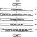
- FIG. 4 is a flowchart illustrating a method of controlling a modulation index of an analog optical signal according to an example embodiment.
- the divider 110 may divide an analog optical signal for a first path and a second path.
- the optical carrier recovery 120 may extract an optical carrier from an analog optical signal divided for the first path in operation 410 .
- the optical carrier recovery 120 may control an intensity of the optical carrier extracted in operation 420 .
- the optical carrier recovery 120 may control the intensity of the optical carrier based on a target value of the modulation index to be controlled.
- the phase shifter 130 may control a phase of the optical carrier of which the intensity is controlled in operation 420 .
- a process of controlling the phase of the optical carrier using the phase shifter 130 will be described with reference to FIG. 5 .
- the coupler 150 may control the modulation index of the analog optical signal by combining the analog optical signal divided for the second path in operation 410 and the optical carrier of which the phase is controlled in operation 440 so as to output the analog optical signal.
- FIG. 5 is a flowchart illustrating a phase control process in a method of controlling a modulation index of an analog optical signal according to an example embodiment. Operations 510 through 530 of FIG. 5 may be included in operation 440 of FIG. 4 .
- the controller 160 may determine whether a modulation index is to be increased. In this example, the controller 160 may determine whether a modulation index is to be increased by monitoring an analog optical signal having a modulation index controlled in the coupler 150 and output from the coupler 150 . When the modulation index is to be increased, the controller 160 may perform operation 530 . When the modulation index is to be reduced, the controller 160 may perform operation 520 .
- the controller 160 may request the phase shifter 130 to change a phase of an optical carrier to be 180° such that a destructive interference occurs in the coupler 150 .
- the phase shifter 130 may change the phase of an optical carrier of which an intensity is controlled in operation 420 , to 180°.
- the controller 160 may request the phase shifter 130 not to change the phase of the optical carrier such that a constructive interference occurs in the coupler 150 .
- the phase shifter 130 may output the phase of an optical carrier of which an intensity is controlled in operation 420 without changing.
- the components described in the exemplary embodiments of the present invention may be achieved by hardware components including at least one DSP (Digital Signal Processor), a processor, a controller, an ASIC (Application Specific Integrated Circuit), a programmable logic element such as an FPGA (Field Programmable Gate Array), other electronic devices, and combinations thereof.
- DSP Digital Signal Processor
- ASIC Application Specific Integrated Circuit
- FPGA Field Programmable Gate Array
- At least some of the functions or the processes described in the exemplary embodiments of the present invention may be achieved by software, and the software may be recorded on a recording medium.
- the components, the functions, and the processes described in the exemplary embodiments of the present invention may be achieved by a combination of hardware and software.
- the method according to example embodiments may be embodied as a program that is executable by a computer and may be implemented as various recording media such as a magnetic storage medium, an optical reading medium, and a digital storage medium.
- Various techniques described herein may be implemented as digital electronic circuitry, or as computer hardware, firmware, software, or combinations thereof.
- the techniques may be implemented as a computer program product, i.e., a computer program tangibly embodied in an information carrier, e.g., in a machine-readable storage device (for example, a computer-readable medium) or in a propagated signal for processing by, or to control an operation of a data processing apparatus, e.g., a programmable processor, a computer, or multiple computers.
- a computer program(s) may be written in any form of a programming language, including compiled or interpreted languages and may be deployed in any form including a stand-alone program or a module, a component, a subroutine, or other units suitable for use in a computing environment.
- a computer program may be deployed to be executed on one computer or on multiple computers at one site or distributed across multiple sites and interconnected by a communication network.
- processors suitable for execution of a computer program include, by way of example, both general and special purpose microprocessors, and any one or more processors of any kind of digital computer.
- a processor will receive instructions and data from a read-only memory or a random access memory or both.
- Elements of a computer may include at least one processor to execute instructions and one or more memory devices to store instructions and data.
- a computer will also include or be coupled to receive data from, transfer data to, or perform both on one or more mass storage devices to store data, e.g., magnetic, magneto-optical disks, or optical disks.
- Examples of information carriers suitable for embodying computer program instructions and data include semiconductor memory devices, for example, magnetic media such as a hard disk, a floppy disk, and a magnetic tape, optical media such as a compact disk read only memory (CD-ROM), a digital video disk (DVD), etc. and magneto-optical media such as a floptical disk, and a read only memory (ROM), a random access memory (RAM), a flash memory, an erasable programmable ROM (EPROM), and an electrically erasable programmable ROM (EEPROM).
- a processor and a memory may be supplemented by, or integrated into, a special purpose logic circuit.
- non-transitory computer-readable media may be any available media that may be accessed by a computer and may include both computer storage media and transmission media.
Landscapes
- Physics & Mathematics (AREA)
- Electromagnetism (AREA)
- Engineering & Computer Science (AREA)
- Computer Networks & Wireless Communication (AREA)
- Signal Processing (AREA)
- Nonlinear Science (AREA)
- Optical Modulation, Optical Deflection, Nonlinear Optics, Optical Demodulation, Optical Logic Elements (AREA)
- Optical Communication System (AREA)
Abstract
Description
Claims (10)
Applications Claiming Priority (2)
| Application Number | Priority Date | Filing Date | Title |
|---|---|---|---|
| KR1020170161262A KR102336106B1 (en) | 2017-11-29 | 2017-11-29 | Apparatus and method for adjusting the modulation index of an analog optical signal using interference phenomenon of coherent light |
| KR10-2017-0161262 | 2017-11-29 |
Publications (2)
| Publication Number | Publication Date |
|---|---|
| US20190165866A1 US20190165866A1 (en) | 2019-05-30 |
| US10560196B2 true US10560196B2 (en) | 2020-02-11 |
Family
ID=66633700
Family Applications (1)
| Application Number | Title | Priority Date | Filing Date |
|---|---|---|---|
| US16/197,793 Expired - Fee Related US10560196B2 (en) | 2017-11-29 | 2018-11-21 | Apparatus and method for adjusting modulation index of analog optical signal using interference phenomenon of coherent light |
Country Status (2)
| Country | Link |
|---|---|
| US (1) | US10560196B2 (en) |
| KR (1) | KR102336106B1 (en) |
Families Citing this family (2)
| Publication number | Priority date | Publication date | Assignee | Title |
|---|---|---|---|---|
| KR102336106B1 (en) * | 2017-11-29 | 2021-12-08 | 한국전자통신연구원 | Apparatus and method for adjusting the modulation index of an analog optical signal using interference phenomenon of coherent light |
| CN117081677B (en) * | 2023-10-13 | 2023-12-15 | 湖北大学 | Method and device for processing inter-carrier injury in SEFDM system |
Citations (12)
| Publication number | Priority date | Publication date | Assignee | Title |
|---|---|---|---|---|
| US5774217A (en) * | 1995-11-17 | 1998-06-30 | Electronics And Telecommunications Research Institute | Measurement of nonlinear refractive index coefficient of optical fiber by Sagnac interferometer |
| US5973820A (en) * | 1997-05-19 | 1999-10-26 | Matsushita Electric Industrial Co., Ltd. | FM modulation device |
| US6211996B1 (en) * | 1999-05-19 | 2001-04-03 | Matsushita Electric Industrial Co., Ltd. | Angle modulator |
| US20050286908A1 (en) * | 2004-06-15 | 2005-12-29 | Way Winston I | Optical communication using duobinary modulation |
| KR100875468B1 (en) | 2006-12-08 | 2008-12-22 | (주)에프씨아이 | AS transmitter with adjustable modulation index |
| US7474858B2 (en) | 2003-08-27 | 2009-01-06 | Samsung Electronics Co., Ltd. | Duobinary optical transmission device using at least one semiconductor optical amplifier |
| US8165474B2 (en) | 2008-03-21 | 2012-04-24 | Applied Optoelectronics, Inc. | Reducing cross modulation in multichannel modulated optical systems with anti-clipping |
| WO2015023028A1 (en) | 2013-08-12 | 2015-02-19 | 한국과학기술원 | Spintronics wireless communication system for simultaneously modulating multiband frequency and amplitude |
| US9130675B2 (en) | 2011-12-30 | 2015-09-08 | Electronics And Telecommunications Research Institute | Signal transmission apparatus and optical modem modulation method |
| US9191121B2 (en) | 2013-03-27 | 2015-11-17 | Electronics And Telecommunications Research Institute | Optical transmitter and method thereof |
| US9787395B2 (en) * | 2015-01-27 | 2017-10-10 | Electronics And Telecommunications Research Institute | Control apparatus and method for monitoring optical fiber link |
| US20190165866A1 (en) * | 2017-11-29 | 2019-05-30 | Electronics And Telecommunications Research Institute | Apparatus and method for adjusting modulation index of analog optical signal using interference phenomenon of coherent light |
-
2017
- 2017-11-29 KR KR1020170161262A patent/KR102336106B1/en active Active
-
2018
- 2018-11-21 US US16/197,793 patent/US10560196B2/en not_active Expired - Fee Related
Patent Citations (12)
| Publication number | Priority date | Publication date | Assignee | Title |
|---|---|---|---|---|
| US5774217A (en) * | 1995-11-17 | 1998-06-30 | Electronics And Telecommunications Research Institute | Measurement of nonlinear refractive index coefficient of optical fiber by Sagnac interferometer |
| US5973820A (en) * | 1997-05-19 | 1999-10-26 | Matsushita Electric Industrial Co., Ltd. | FM modulation device |
| US6211996B1 (en) * | 1999-05-19 | 2001-04-03 | Matsushita Electric Industrial Co., Ltd. | Angle modulator |
| US7474858B2 (en) | 2003-08-27 | 2009-01-06 | Samsung Electronics Co., Ltd. | Duobinary optical transmission device using at least one semiconductor optical amplifier |
| US20050286908A1 (en) * | 2004-06-15 | 2005-12-29 | Way Winston I | Optical communication using duobinary modulation |
| KR100875468B1 (en) | 2006-12-08 | 2008-12-22 | (주)에프씨아이 | AS transmitter with adjustable modulation index |
| US8165474B2 (en) | 2008-03-21 | 2012-04-24 | Applied Optoelectronics, Inc. | Reducing cross modulation in multichannel modulated optical systems with anti-clipping |
| US9130675B2 (en) | 2011-12-30 | 2015-09-08 | Electronics And Telecommunications Research Institute | Signal transmission apparatus and optical modem modulation method |
| US9191121B2 (en) | 2013-03-27 | 2015-11-17 | Electronics And Telecommunications Research Institute | Optical transmitter and method thereof |
| WO2015023028A1 (en) | 2013-08-12 | 2015-02-19 | 한국과학기술원 | Spintronics wireless communication system for simultaneously modulating multiband frequency and amplitude |
| US9787395B2 (en) * | 2015-01-27 | 2017-10-10 | Electronics And Telecommunications Research Institute | Control apparatus and method for monitoring optical fiber link |
| US20190165866A1 (en) * | 2017-11-29 | 2019-05-30 | Electronics And Telecommunications Research Institute | Apparatus and method for adjusting modulation index of analog optical signal using interference phenomenon of coherent light |
Non-Patent Citations (1)
| Title |
|---|
| Zhang et al ; Optical single side band polarization modulation for radio-over-fiber system and microwave photonic signal processing; Aug. 2014; pp. 80-85 (Year: 2014). * |
Also Published As
| Publication number | Publication date |
|---|---|
| KR102336106B1 (en) | 2021-12-08 |
| US20190165866A1 (en) | 2019-05-30 |
| KR20190062752A (en) | 2019-06-07 |
Similar Documents
| Publication | Publication Date | Title |
|---|---|---|
| US9380471B2 (en) | Method, apparatus and system of determining a time of arrival of a wireless communication signal | |
| US11985486B2 (en) | Sound signal processing method, apparatus and device based on microphone array | |
| US10627501B2 (en) | Pulse radar apparatus and operating method of pulse radar apparatus | |
| CN104967635A (en) | Data transmission method and apparatus thereof | |
| US10560196B2 (en) | Apparatus and method for adjusting modulation index of analog optical signal using interference phenomenon of coherent light | |
| US10009000B2 (en) | RFID reader antenna port isolation | |
| TW201824815A (en) | Efficient control mechanism in distributed antenna modules | |
| US11528062B2 (en) | Method and device for virtual port mapping for massive MIMO | |
| WO2021087759A1 (en) | Co-frequency interference suppression method, linear frequency modulation continuous wave radar, mobile platform, and storage medium | |
| US10616811B2 (en) | Methods and apparatus for using a communication protocol based on a wireless network | |
| US20190261440A1 (en) | Electronic device and wireless connection control method of electronic device | |
| US20220279490A1 (en) | Method, apparatus, and device of processing terminal capability | |
| US10003408B2 (en) | Receiving method and receiver device for a coherent optical communication system | |
| US20250096851A1 (en) | Beam configuration techniques for reconfigurable intelligent surface in wireless communication system | |
| EP4207887A1 (en) | Method and apparatus for determining time delay compensation value, and device and storage medium | |
| CN109120290B (en) | RFID receiving circuit, storage medium, and electronic device | |
| KR20200098363A (en) | Method and apparatus for tracking frequency hopping signal in mobile communication system | |
| US20220311591A1 (en) | KRAMERS-KRONIG RECEPTION-BASED THz SIGNAL RECEPTION APPARATUS AND FREQUENCY OFFSET COMPENSATION METHOD USING THE SAME | |
| KR101923997B1 (en) | Method for controlling antenna switching of a tracking transponder having a single transceiver | |
| KR20250021738A (en) | Active jamming system and method | |
| KR101925923B1 (en) | Wireless power transfer apparatus based on adaptive phase reversal using cancellation loop and method thereof | |
| KR102076745B1 (en) | Apparatus, system and method for self-interference cancellation using vector modulator | |
| US20140354478A1 (en) | Communication system, control apparatus, control method, and storage medium | |
| KR102602390B1 (en) | Apparatus and method for estimating delay time in synchronization system | |
| US12381625B2 (en) | Free space optical communication device, free space optical communication system, and free space optical communication method |
Legal Events
| Date | Code | Title | Description |
|---|---|---|---|
| FEPP | Fee payment procedure |
Free format text: ENTITY STATUS SET TO UNDISCOUNTED (ORIGINAL EVENT CODE: BIG.); ENTITY STATUS OF PATENT OWNER: SMALL ENTITY |
|
| AS | Assignment |
Owner name: ELECTRONICS AND TELECOMMUNICATIONS RESEARCH INSTIT Free format text: ASSIGNMENT OF ASSIGNORS INTEREST;ASSIGNORS:KIM, JOONYOUNG;SUNG, MINKYU;LEE, JONG HYUN;AND OTHERS;REEL/FRAME:047587/0766 Effective date: 20181109 Owner name: ELECTRONICS AND TELECOMMUNICATIONS RESEARCH INSTITUTE, KOREA, REPUBLIC OF Free format text: ASSIGNMENT OF ASSIGNORS INTEREST;ASSIGNORS:KIM, JOONYOUNG;SUNG, MINKYU;LEE, JONG HYUN;AND OTHERS;REEL/FRAME:047587/0766 Effective date: 20181109 |
|
| FEPP | Fee payment procedure |
Free format text: ENTITY STATUS SET TO SMALL (ORIGINAL EVENT CODE: SMAL); ENTITY STATUS OF PATENT OWNER: SMALL ENTITY |
|
| STPP | Information on status: patent application and granting procedure in general |
Free format text: DOCKETED NEW CASE - READY FOR EXAMINATION |
|
| STPP | Information on status: patent application and granting procedure in general |
Free format text: NON FINAL ACTION MAILED |
|
| STPP | Information on status: patent application and granting procedure in general |
Free format text: RESPONSE TO NON-FINAL OFFICE ACTION ENTERED AND FORWARDED TO EXAMINER |
|
| STPP | Information on status: patent application and granting procedure in general |
Free format text: NOTICE OF ALLOWANCE MAILED -- APPLICATION RECEIVED IN OFFICE OF PUBLICATIONS |
|
| STPP | Information on status: patent application and granting procedure in general |
Free format text: PUBLICATIONS -- ISSUE FEE PAYMENT VERIFIED |
|
| STCF | Information on status: patent grant |
Free format text: PATENTED CASE |
|
| FEPP | Fee payment procedure |
Free format text: MAINTENANCE FEE REMINDER MAILED (ORIGINAL EVENT CODE: REM.); ENTITY STATUS OF PATENT OWNER: SMALL ENTITY |
|
| LAPS | Lapse for failure to pay maintenance fees |
Free format text: PATENT EXPIRED FOR FAILURE TO PAY MAINTENANCE FEES (ORIGINAL EVENT CODE: EXP.); ENTITY STATUS OF PATENT OWNER: SMALL ENTITY |
|
| STCH | Information on status: patent discontinuation |
Free format text: PATENT EXPIRED DUE TO NONPAYMENT OF MAINTENANCE FEES UNDER 37 CFR 1.362 |
|
| FP | Lapsed due to failure to pay maintenance fee |
Effective date: 20240211 |