US10559282B2 - Pixel driving circuits for switching display resolution, driving methods thereof and display apparatuses - Google Patents
Pixel driving circuits for switching display resolution, driving methods thereof and display apparatuses Download PDFInfo
- Publication number
- US10559282B2 US10559282B2 US15/793,957 US201715793957A US10559282B2 US 10559282 B2 US10559282 B2 US 10559282B2 US 201715793957 A US201715793957 A US 201715793957A US 10559282 B2 US10559282 B2 US 10559282B2
- Authority
- US
- United States
- Prior art keywords
- data line
- switch
- display
- turned
- driving circuit
- Prior art date
- Legal status (The legal status is an assumption and is not a legal conclusion. Google has not performed a legal analysis and makes no representation as to the accuracy of the status listed.)
- Expired - Fee Related, expires
Links
- 238000000034 method Methods 0.000 title claims abstract description 19
- 238000010586 diagram Methods 0.000 description 5
- 239000010409 thin film Substances 0.000 description 4
- 230000000694 effects Effects 0.000 description 3
- 239000000463 material Substances 0.000 description 1
- 230000011664 signaling Effects 0.000 description 1
- 238000006467 substitution reaction Methods 0.000 description 1
Images


Classifications
-
- G—PHYSICS
- G09—EDUCATION; CRYPTOGRAPHY; DISPLAY; ADVERTISING; SEALS
- G09G—ARRANGEMENTS OR CIRCUITS FOR CONTROL OF INDICATING DEVICES USING STATIC MEANS TO PRESENT VARIABLE INFORMATION
- G09G5/00—Control arrangements or circuits for visual indicators common to cathode-ray tube indicators and other visual indicators
- G09G5/22—Control arrangements or circuits for visual indicators common to cathode-ray tube indicators and other visual indicators characterised by the display of characters or indicia using display control signals derived from coded signals representing the characters or indicia, e.g. with a character-code memory
- G09G5/222—Control of the character-code memory
- G09G5/227—Resolution modifying circuits, e.g. variable screen formats, resolution change between memory contents and display screen
-
- G—PHYSICS
- G09—EDUCATION; CRYPTOGRAPHY; DISPLAY; ADVERTISING; SEALS
- G09G—ARRANGEMENTS OR CIRCUITS FOR CONTROL OF INDICATING DEVICES USING STATIC MEANS TO PRESENT VARIABLE INFORMATION
- G09G3/00—Control arrangements or circuits, of interest only in connection with visual indicators other than cathode-ray tubes
- G09G3/20—Control arrangements or circuits, of interest only in connection with visual indicators other than cathode-ray tubes for presentation of an assembly of a number of characters, e.g. a page, by composing the assembly by combination of individual elements arranged in a matrix no fixed position being assigned to or needed to be assigned to the individual characters or partial characters
- G09G3/2092—Details of a display terminals using a flat panel, the details relating to the control arrangement of the display terminal and to the interfaces thereto
-
- G—PHYSICS
- G09—EDUCATION; CRYPTOGRAPHY; DISPLAY; ADVERTISING; SEALS
- G09G—ARRANGEMENTS OR CIRCUITS FOR CONTROL OF INDICATING DEVICES USING STATIC MEANS TO PRESENT VARIABLE INFORMATION
- G09G3/00—Control arrangements or circuits, of interest only in connection with visual indicators other than cathode-ray tubes
- G09G3/20—Control arrangements or circuits, of interest only in connection with visual indicators other than cathode-ray tubes for presentation of an assembly of a number of characters, e.g. a page, by composing the assembly by combination of individual elements arranged in a matrix no fixed position being assigned to or needed to be assigned to the individual characters or partial characters
- G09G3/34—Control arrangements or circuits, of interest only in connection with visual indicators other than cathode-ray tubes for presentation of an assembly of a number of characters, e.g. a page, by composing the assembly by combination of individual elements arranged in a matrix no fixed position being assigned to or needed to be assigned to the individual characters or partial characters by control of light from an independent source
- G09G3/36—Control arrangements or circuits, of interest only in connection with visual indicators other than cathode-ray tubes for presentation of an assembly of a number of characters, e.g. a page, by composing the assembly by combination of individual elements arranged in a matrix no fixed position being assigned to or needed to be assigned to the individual characters or partial characters by control of light from an independent source using liquid crystals
- G09G3/3611—Control of matrices with row and column drivers
- G09G3/3685—Details of drivers for data electrodes
-
- G—PHYSICS
- G09—EDUCATION; CRYPTOGRAPHY; DISPLAY; ADVERTISING; SEALS
- G09G—ARRANGEMENTS OR CIRCUITS FOR CONTROL OF INDICATING DEVICES USING STATIC MEANS TO PRESENT VARIABLE INFORMATION
- G09G5/00—Control arrangements or circuits for visual indicators common to cathode-ray tube indicators and other visual indicators
- G09G5/003—Details of a display terminal, the details relating to the control arrangement of the display terminal and to the interfaces thereto
-
- G—PHYSICS
- G09—EDUCATION; CRYPTOGRAPHY; DISPLAY; ADVERTISING; SEALS
- G09G—ARRANGEMENTS OR CIRCUITS FOR CONTROL OF INDICATING DEVICES USING STATIC MEANS TO PRESENT VARIABLE INFORMATION
- G09G2300/00—Aspects of the constitution of display devices
- G09G2300/04—Structural and physical details of display devices
- G09G2300/0439—Pixel structures
- G09G2300/0452—Details of colour pixel setup, e.g. pixel composed of a red, a blue and two green components
-
- G—PHYSICS
- G09—EDUCATION; CRYPTOGRAPHY; DISPLAY; ADVERTISING; SEALS
- G09G—ARRANGEMENTS OR CIRCUITS FOR CONTROL OF INDICATING DEVICES USING STATIC MEANS TO PRESENT VARIABLE INFORMATION
- G09G2300/00—Aspects of the constitution of display devices
- G09G2300/08—Active matrix structure, i.e. with use of active elements, inclusive of non-linear two terminal elements, in the pixels together with light emitting or modulating elements
- G09G2300/0809—Several active elements per pixel in active matrix panels
-
- G—PHYSICS
- G09—EDUCATION; CRYPTOGRAPHY; DISPLAY; ADVERTISING; SEALS
- G09G—ARRANGEMENTS OR CIRCUITS FOR CONTROL OF INDICATING DEVICES USING STATIC MEANS TO PRESENT VARIABLE INFORMATION
- G09G2310/00—Command of the display device
- G09G2310/02—Addressing, scanning or driving the display screen or processing steps related thereto
- G09G2310/0243—Details of the generation of driving signals
-
- G—PHYSICS
- G09—EDUCATION; CRYPTOGRAPHY; DISPLAY; ADVERTISING; SEALS
- G09G—ARRANGEMENTS OR CIRCUITS FOR CONTROL OF INDICATING DEVICES USING STATIC MEANS TO PRESENT VARIABLE INFORMATION
- G09G2310/00—Command of the display device
- G09G2310/02—Addressing, scanning or driving the display screen or processing steps related thereto
- G09G2310/0264—Details of driving circuits
- G09G2310/0275—Details of drivers for data electrodes, other than drivers for liquid crystal, plasma or OLED displays, not related to handling digital grey scale data or to communication of data to the pixels by means of a current
-
- G—PHYSICS
- G09—EDUCATION; CRYPTOGRAPHY; DISPLAY; ADVERTISING; SEALS
- G09G—ARRANGEMENTS OR CIRCUITS FOR CONTROL OF INDICATING DEVICES USING STATIC MEANS TO PRESENT VARIABLE INFORMATION
- G09G2310/00—Command of the display device
- G09G2310/02—Addressing, scanning or driving the display screen or processing steps related thereto
- G09G2310/0264—Details of driving circuits
- G09G2310/0291—Details of output amplifiers or buffers arranged for use in a driving circuit
-
- G—PHYSICS
- G09—EDUCATION; CRYPTOGRAPHY; DISPLAY; ADVERTISING; SEALS
- G09G—ARRANGEMENTS OR CIRCUITS FOR CONTROL OF INDICATING DEVICES USING STATIC MEANS TO PRESENT VARIABLE INFORMATION
- G09G2330/00—Aspects of power supply; Aspects of display protection and defect management
- G09G2330/02—Details of power systems and of start or stop of display operation
- G09G2330/021—Power management, e.g. power saving
-
- G—PHYSICS
- G09—EDUCATION; CRYPTOGRAPHY; DISPLAY; ADVERTISING; SEALS
- G09G—ARRANGEMENTS OR CIRCUITS FOR CONTROL OF INDICATING DEVICES USING STATIC MEANS TO PRESENT VARIABLE INFORMATION
- G09G2340/00—Aspects of display data processing
- G09G2340/04—Changes in size, position or resolution of an image
- G09G2340/0407—Resolution change, inclusive of the use of different resolutions for different screen areas
- G09G2340/0421—Horizontal resolution change
-
- G—PHYSICS
- G09—EDUCATION; CRYPTOGRAPHY; DISPLAY; ADVERTISING; SEALS
- G09G—ARRANGEMENTS OR CIRCUITS FOR CONTROL OF INDICATING DEVICES USING STATIC MEANS TO PRESENT VARIABLE INFORMATION
- G09G3/00—Control arrangements or circuits, of interest only in connection with visual indicators other than cathode-ray tubes
- G09G3/20—Control arrangements or circuits, of interest only in connection with visual indicators other than cathode-ray tubes for presentation of an assembly of a number of characters, e.g. a page, by composing the assembly by combination of individual elements arranged in a matrix no fixed position being assigned to or needed to be assigned to the individual characters or partial characters
- G09G3/34—Control arrangements or circuits, of interest only in connection with visual indicators other than cathode-ray tubes for presentation of an assembly of a number of characters, e.g. a page, by composing the assembly by combination of individual elements arranged in a matrix no fixed position being assigned to or needed to be assigned to the individual characters or partial characters by control of light from an independent source
- G09G3/36—Control arrangements or circuits, of interest only in connection with visual indicators other than cathode-ray tubes for presentation of an assembly of a number of characters, e.g. a page, by composing the assembly by combination of individual elements arranged in a matrix no fixed position being assigned to or needed to be assigned to the individual characters or partial characters by control of light from an independent source using liquid crystals
- G09G3/3611—Control of matrices with row and column drivers
- G09G3/3614—Control of polarity reversal in general
Definitions
- the present disclosure relates to the field of display technology, and more particularly, to a driving circuit, a driving method thereof, and a display apparatus.
- a maximum number of pixels which may be displayed on a display screen is called a physical resolution of the display screen, which is a parameter inherent to the display screen.
- resolutions of other areas may be reduced.
- the present disclosure provides a pixel driving circuit, a driving method thereof, and a display apparatus, to realize switch between display resolutions.
- the N data lines in the pixel driving circuit comprise remaining N ⁇ r ⁇ k data lines.
- conventional signal control devices may be provided on the remaining N ⁇ r ⁇ k data lines so that these signal control devices are used in cooperation with the first switch unit and the second switch unit respectively to realize multi-resolution display.
- the remaining N ⁇ r ⁇ k data lines may also normally output data, and the display apparatus which is driven by the pixel driving circuit according to the present disclosure can display at different resolutions only through operations of the first switch unit and the second switch unit.
- a pixel driving method applied to the pixel driving circuit described above comprising:
- the signal control unit controlling, by the signal control unit, the first switch unit to be turned off and the second switch to be turned on when display is to be performed at the second resolution.
- a display apparatus comprising the pixel driving circuit described above.
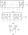
- FIG. 1 is a structural diagram of a pixel driving circuit according to an embodiment of the present disclosure
- FIG. 2 is a structural diagram of a pixel driving circuit according to another embodiment of the present disclosure.
- FIG. 3 is a structural diagram of a pixel driving circuit according to another embodiment of the present disclosure.
- FIG. 4 is a structural diagram of a pixel driving circuit according to another embodiment of the present disclosure.
- FIG. 5 is a structural diagram of a pixel driving circuit according to another embodiment of the present disclosure.
- a pixel driving circuit may comprise N data lines which are denoted by D 1 , D 2 , . . . , D N-2 , D N-1 and D N in turn in FIG. 1 .
- the first switch unit and the second switch unit are connected to a signal control unit SW respectively, wherein the signal control unit SW is configured to control the first switch unit to be turned on and the second switch unit to be turned off when display is to be performed at a first resolution.
- the signal control unit SW is further configured to control the first switch unit to be turned off and the second switch unit to be turned on when display is to be performed at a second resolution, wherein the first resolution is greater than the second resolution.
- the signal control unit SW controls the first switch unit to be turned on and the second switch unit to be turned off.
- the signal control unit SW controls the first switch unit to be turned off and the second switch unit to be turned on.
- each of the first data lines has a first switch unit provided thereon and is connected to corresponding q second data lines through a second switch unit.
- the signal control unit SW may control the first switch unit to be turned on and the second switch unit to be turned off, so that a pixel unit is driven individually by each of the first data lines and corresponding second data lines respectively, thereby driving a display panel to display at the higher first resolution.
- the signal control unit SW controls the first switch unit to be turned off and the second switch unit to be turned on, so that the first data line is connected to the corresponding q second data lines through the second switch unit, and data output is shared by each of the first data lines and the corresponding q second data lines, thereby transmitting the same data driving signal through a plurality of data lines.
- a plurality of pixels corresponding to the plurality of data lines are considered to be one pixel, which is equivalent to reducing a number of pixels per area, i.e., realizing display at the lower second resolution. Therefore, in the pixel driving circuit according to the embodiments of the present disclosure, operations of the first switch unit and the second switch unit are controlled by the signal control unit SW, so that the display apparatus which is driven by the pixel driving circuit can realize display at different resolutions.
- the N data lines in the pixel driving circuit comprise remaining N ⁇ r ⁇ k data lines.
- the remaining N ⁇ r ⁇ k data lines conventional signal control devices may be provided on the remaining N ⁇ r ⁇ k data lines so that these signal control devices are used in cooperation with the first switch unit and the second switch unit respectively to realize multi-resolution display.
- the remaining N ⁇ r ⁇ k data lines may also normally output data, and the display apparatus which is driven by the pixel driving circuit according to the embodiments of the present disclosure can display at different resolutions only through operations of the first switch unit and the second switch unit.
- a current first data line is an i th data line in the N data lines, so that the q second data lines corresponding to the current first data line is a j th data line to a (j+q ⁇ 1) th data line.
- the current first data line is the i th data line and the second data line is an (i+1) th data line. That is, the second data line is arranged adjacent to the first data line in this case.
- FIG. 1 a structure of the pixel driving circuit is shown in FIG. 1 .
- the signal control unit SW controls the first switch unit to be turned on and the second switch unit to be turned off.
- a pixel unit is driven individually by the first data line and the second data line respectively, so that the display panel which is driven by the pixel driving circuit displays at the higher first resolution.
- the signal control unit SW controls the first switch unit to be turned off and the second switch unit to be turned on, so that the first data line is connected to the second data line through the second switch unit, and data output is shared by the first data line and the second data line, to realize display at the lower second resolution.
- the second data line corresponding to the current first data line is an (i+m ⁇ 1) th data line.
- the second data line connected to the first data line through the second switch unit is separated from the first data line by m ⁇ 2 data lines.
- the pixel unit may comprise a red sub-pixel, a green sub-pixel, and a blue sub-pixel.
- the pixel unit may comprise a red sub-pixel, a green sub-pixel, a blue sub-pixel, and a white sub-pixel.
- the pixel unit is driven individually by the first data line and the second data line respectively, so that the display panel which is driven by the pixel driving circuit displays at the higher first resolution.
- the signal control unit SW controls the first switch unit to be turned off and the second switch unit to be turned on, so that the first data line is connected to the second data line through the second switch unit, and data output is shared by the first data line and the second data line, to realize display at the lower second resolution.
- the current first data line is the i th data line
- the q second data lines corresponding to the current first data line are an (i+1) th data line to an (i+q) th data line.
- the at least two second data lines corresponding to the first data line are arranged adjacent to the first data line.
- the current first data line is a first data line
- the three second data lines corresponding to the current first data line are a second data line, a third data line and a fourth data line.
- the signal control unit SW controls the first switch unit to be turned on and the second switch unit to be turned off.
- the pixel unit is driven individually by the first data line and the second data lines respectively, so that the display panel which is driven by the pixel driving circuit displays at the higher first resolution.
- the signal control unit SW controls the first switch unit to be turned off and the second switch unit to be turned on, so that the first data line is connected to the second data lines through the second switch unit, and data output is shared by the first data line and the second data lines, to realize display at the lower second resolution.
- the q second data lines corresponding to the current first data line are an (i+m ⁇ 1) th data line to an (i+q+m ⁇ 2) th data line.
- the signal control unit SW controls the first switch unit to be turned on and the second switch unit to be turned off.
- the pixel unit is driven individually by the first data line and the second data lines respectively, so that the display panel which is driven by the pixel driving circuit displays at the higher first resolution.
- the signal control unit SW controls the first switch unit to be turned off and the second switch unit to be turned on, so that the first data line is connected to the second data lines through the second switch unit, and data output is shared by the first data line and the second data lines, to realize display at the lower second resolution.
- the q second data lines corresponding to the current first data line are an (i+m ⁇ 1) th data line, an (i+2(m ⁇ 1)) th data line, an (i+3(m ⁇ 1)) th data line, . . . , an (i+(q ⁇ 1)(m ⁇ 1)) th data line, and an (i+q(m ⁇ 1)) th data line. That is, a first one of the q second data lines is separated from the first data line by m ⁇ 2 data lines, and adjacent two second data lines of the q second data lines are spaced by m ⁇ 2 data lines.
- the second data lines connected to the first data line are arranged at intervals, so that when display is to be performed at the lower second resolution, data output is shared by the plurality of data lines which are arranged at equal intervals, so as to realize a more uniform display effect of the display panel which is driven by the pixel driving circuit.
- each of the first data lines in the N data lines is connected to three second data lines through the second switch unit, and the current first data line is a first data line, and the second data lines are a third data line, a fifth data line and a seventh data line.
- the signal control unit SW controls the first switch unit to be turned on and the second switch unit to be turned off.
- the pixel unit is driven individually by the first data line and the second data line respectively, so that the display panel which is driven by the pixel driving circuit displays at the higher first resolution.
- the signal control unit SW controls the first switch unit to be turned off and the second switch unit to be turned on, so that the first data line is connected to the second data lines through the second switch unit, and data output is shared by the first data line and the second data lines, to realize display at the lower second resolution.
- the first data lines comprise an i th data line and an (i+1) th data line (e.g. data lines D 1 and D 2 in FIG. 5 ).
- the first switch unit comprises a first switch SW 1 which is provided on respective first data line.
- each of the data lines D 1 and D 2 has a respective first switch SW 1 provided thereon.
- the data line D 1 has one terminal connected to a voltage output terminal of the pixel driving circuit in order to output data driving signal to a corresponding thin film transistor in the display panel, and the other terminal connected to a voltage output terminal of the operational amplifier OP 1 .
- the operational amplifier OP 2 has a voltage output terminal connected to one terminal of the data line D 2 , the data line D 2 has the other terminal connected to a voltage output terminal of the pixel driving circuit in order to output data driving signal to a corresponding thin film transistor in the display panel.
- Each of the operational amplifiers OP 1 and OP 2 has a first power supply input terminal connected to a power supply and a second power supply input terminal connected to the ground.
- the second data lines comprises a i th data line and a (j+1) th data line (e.g. data lines D 3 and D 4 in FIG. 5 ), and the second switch unit comprises a second switch SW 2 .
- the data line D 3 has one terminal connected to a voltage output terminal of the pixel driving circuit in order to output data driving signal to a corresponding thin film transistor in the display panel, and the other terminal connected to a voltage output terminal of the operational amplifier OP 3 .
- the operational amplifier OP 4 has a voltage output terminal connected to one terminal of the data line D 4 .
- the data line D 4 has the other terminal connected to a voltage output terminal of the pixel driving circuit in order to output data driving signal to a corresponding thin film transistor in the display panel.
- Each of the operational amplifiers OP 3 and OP 4 has a first power supply input terminal connected to the power supply, and a second power supply input terminal connected to the ground.
- the first switches SW 1 and the second switches SW 2 are connected to the signal control unit SW respectively.
- the signal control unit SW is configured to output a first level signal under the first resolution, so that the first level signal controls the first switch to be turned on and the second switch to be turned off.
- the signal control unit SW is further configured to output a second level signal when display is to be performed at the second resolution, so that the second level signal controls the first switch to be turned off and the second switch to be turned on.
- the signal control unit SW may be used to output the first level signal under the first resolution, so that the first level signal controls the first switch SW 1 to be turned on and the second switch SW 2 to be turned off.
- the pixel unit is driven individually by each of the first data lines and corresponding second data lines respectively, so that the display apparatus which is driven by the pixel driving circuit realizes display at the higher first resolution.
- the signal control unit SW may be used to output the second level signal under the second resolution, so that the second level signal controls the first switch to be turned off and the second switch to be turned on, so as to enable the pixel driving circuit to realize an effect of display at the second resolution.
- the second switch SW 2 is connected to the data line D 1 and the data line D 3 ; or the second switch SW 2 is connected to the data line D 1 and the data line D 4 ; or the second switch SW 2 is connected to the data line D 2 and the data line D 3 ; or the second switch SW 2 is connected to the data line D 2 and the data line D 4 .
- the first power supply input terminal of the first operational amplifier OP 1 or the second operational amplifier OP 2 is further connected to a third switch.
- a third switch As shown in FIG. 4 , illustrated is a condition that the first power supply input terminal of the second operational amplifier OP 2 is connected to the third switch SW 3 which is connected to the signal control unit SW.
- the signal control unit SW is further configured to output a first level signal under the first resolution, so that the first level signal controls the third switch SW 3 to be turned on.
- the signal control unit SW is configured to output a second level signal under the second resolution, so that the second level signal controls the third switch SW 3 to be turned off.
- the signal control unit SW controls the third switch unit SW 3 to be turned on.
- the signal control unit SW controls the third switch unit SW 3 to be turned off.
- the third switch SW 3 is provided at the first power supply input terminal of the first operational amplifier OP 1 or the second operational amplifier OP 2 . Therefore, when display is to be performed at the first resolution, the first level signal output by the signal control unit SW is used to enable the third switch SW 3 to be turned on.
- the pixel driving circuit according to the present disclosure operates normally under the first resolution even if power is normally supplied by the power supply to the first operational amplifier OP 1 or the second operational amplifier OP 2 connected to the third switch SW 3 .
- the pixel driving circuit may enables the third switch SW 3 to be turned off using the second level signal output by the signal control unit SW when display is to be performed at the second resolution, so that the power supply is disconnected from the first operational amplifier OP 1 or the second operational amplifier OP 2 which is connected to the third switch SW 3 .
- the pixel driving circuit according to the present disclosure operates normally under the second resolution and the power consumption of the pixel driving circuit is reduced.
- the first switch is an N-type transistor
- the second switch is a P-type transistor
- the third switch is an N-type transistor.
- the first switch is a P-type transistor
- the second switch is an N-type transistor
- the third switch is a P-type transistor.
- the pixel driving circuit further comprises a voltage signal control unit connected to each of the data lines.
- the voltage signal control unit is configured to control a data line to output a display signal according to an input voltage.
- a 2i th data line and a (2i+1) th data line are connected to the voltage signal control unit through at least one connection line respectively.
- the voltage signal control unit is configured to control the 2i th data line to output a display signal when the input voltage is a first voltage signal and control the (2i+1) th data line to output a display signal when the input voltage is a second voltage signal.
- the first voltage signal may correspond to a positive polarity voltage
- the second voltage signal may correspond to a negative polarity voltage. As shown in FIG.
- data lines D 1 and D 2 are connected to the voltage signal unit, which controls data line D 1 to output a display signal when the input voltage is a negative polarity voltage, and control data line D 2 to output a display signal when the input voltage is a positive polarity voltage.
- data lines D 3 and D 4 are connected to the voltage signal unit, which controls the data line D 3 to output a display signal when the input voltage is a negative polarity voltage, and control the data line D 4 to output a display signal when the input voltage is a positive polarity voltage.
- data lines controlled by voltage of the same polarity to output display signals are connected with each other. As shown in FIG.
- a first power supply input terminal of the operational amplifier OP 1 is a connected to a second power supply input terminal of the operational amplifier OP 2
- a second power supply input terminal of the operational amplifier OP 1 is connected to the ground
- a first power supply input terminal of the operational amplifier OP 2 is connected to a power supply.
- a first power supply input terminal of the operational amplifier OP 3 is a connected to a second power supply input terminal of the operational amplifier OP 4
- a second power supply input terminal of the operational amplifier OP 3 is connected to the ground
- a first power supply input terminal of the operational amplifier OP 4 is connected to a power supply.
- such relationship is denoted by the cross symbol “X” between output terminals of the two operational amplifiers (e.g. between operational amplifiers OP 1 and OP 2 , or between operational amplifiers OP 3 and OP 4 ).
- the cross symbol “X” indicates that the two operational amplifiers have their power supply terminals connected in series and the two data lines (e.g. data lines D 1 and D 2 , or data lines D 3 and D 4 ) connected to the two operational amplifies are controlled by positive polarity voltage and negative polarity voltage respectively.
- the voltage signal control unit is provided in the pixel driving circuit and the 2i th data line and the (2i+1) th data line are connected to the voltage signal control unit through at least one connection line respectively, so that the voltage signal control unit may be used to control the 2i th data line to output a display signal when the input voltage is a first voltage signal and control the (2i+1) th data line to output a display signal when the input voltage is a second voltage signal.
- the pixel driving circuit according to the present disclosure realizes control of different data lines by different voltage signals, avoids the interference due to different display voltage signals, and improves the display effect of the display apparatus which is driven by the pixel driving circuit.
- the present disclosure provides a pixel driving method, applied to the pixel driving circuit disclosed above.
- the method comprises: controlling, by the signal control unit, the first switch unit to be turned on and the second switch to be turned off when display is to be performed at a first resolution; and controlling, by the signal control unit, the first switch unit to be turned off and the second switch to be turned on when display is to be performed at a second resolution.
- the first switch unit comprises a first operational amplifier OP 1 and a first switch SW 1
- the second switch unit comprises a second operational amplifier OP 2 and a second switch SW 2
- the signal control unit outputs a first level signal when display is to be performed at the first resolution, so that the first level signal controls the first switch unit SW 1 to be turned on and the second switch unit SW 2 to be turned off.
- the signal control unit outputs a second level signal when display is to be performed at the second resolution, so that the second level signal controls the first switch unit SW 1 to be turned off and the second switch unit SW 2 to be turned on.
- the pixel driving method may comprise: outputting, by the signal control unit SW, a first level signal when display is to be performed at the first resolution, so that the first level signal controls the third switch SW 3 to be turned on; and outputting, by the signal control unit SW, a second level signal when display is to be performed at the second resolution, so that the second level signal controls the third switch SW 3 to be turned off.
- the pixel driving method may further comprise:
- the embodiments of the present disclosure further provide a display apparatus, comprising the pixel driving method according to the present disclosure.
Landscapes
- Engineering & Computer Science (AREA)
- Physics & Mathematics (AREA)
- Computer Hardware Design (AREA)
- General Physics & Mathematics (AREA)
- Theoretical Computer Science (AREA)
- Chemical & Material Sciences (AREA)
- Crystallography & Structural Chemistry (AREA)
- Control Of Indicators Other Than Cathode Ray Tubes (AREA)
Abstract
Description
Claims (20)
Applications Claiming Priority (3)
| Application Number | Priority Date | Filing Date | Title |
|---|---|---|---|
| CN201710198860.4A CN106683609B (en) | 2017-03-29 | 2017-03-29 | A pixel driving circuit, a driving method thereof, and a display device |
| CN201710198860.4 | 2017-03-29 | ||
| CN201710198860 | 2017-03-29 |
Publications (2)
| Publication Number | Publication Date |
|---|---|
| US20180286303A1 US20180286303A1 (en) | 2018-10-04 |
| US10559282B2 true US10559282B2 (en) | 2020-02-11 |
Family
ID=58829375
Family Applications (1)
| Application Number | Title | Priority Date | Filing Date |
|---|---|---|---|
| US15/793,957 Expired - Fee Related US10559282B2 (en) | 2017-03-29 | 2017-10-25 | Pixel driving circuits for switching display resolution, driving methods thereof and display apparatuses |
Country Status (2)
| Country | Link |
|---|---|
| US (1) | US10559282B2 (en) |
| CN (1) | CN106683609B (en) |
Cited By (1)
| Publication number | Priority date | Publication date | Assignee | Title |
|---|---|---|---|---|
| US12579930B2 (en) | 2024-05-29 | 2026-03-17 | AUO Corporation | Micro-LED display panel and pixel driving circuit thereof |
Families Citing this family (3)
| Publication number | Priority date | Publication date | Assignee | Title |
|---|---|---|---|---|
| CN113077763B (en) * | 2020-01-06 | 2022-07-05 | 京东方科技集团股份有限公司 | Display panel, display device and driving method |
| EP4339934A4 (en) * | 2021-07-02 | 2024-05-22 | BOE Technology Group Co., Ltd. | Display panel, display device, and method for driving display device |
| EP4339929A4 (en) * | 2021-11-29 | 2024-08-07 | BOE Technology Group Co., Ltd. | DISPLAY SUBSTRATE AND CONTROL METHOD THEREFOR AND DISPLAY DEVICE |
Citations (18)
| Publication number | Priority date | Publication date | Assignee | Title |
|---|---|---|---|---|
| JPS6418193A (en) | 1987-07-14 | 1989-01-20 | Seiko Epson Corp | Matrix type display device |
| US20020000970A1 (en) * | 2000-06-29 | 2002-01-03 | Hajime Akimoto | Image display apparatus |
| US20030214476A1 (en) * | 2002-05-17 | 2003-11-20 | Noboru Matsuda | Signal output device and display device |
| US20040008173A1 (en) * | 2001-11-30 | 2004-01-15 | Kazuhiro Maeda | Signal line drive circuit and display device using the same |
| CN1501706A (en) | 2002-11-12 | 2004-06-02 | 夏普株式会社 | Data signal line driving method, data signal line driving circuit and display device |
| US20050179640A1 (en) * | 2004-02-17 | 2005-08-18 | Noriyuki Tanaka | Display device, drive method thereof, and drive system thereof |
| US20060114210A1 (en) * | 2004-11-30 | 2006-06-01 | Chen Jung-Zone | Power saving flat type display and method thereof |
| CN101047797A (en) | 2006-03-31 | 2007-10-03 | 佳能株式会社 | Image sensor |
| CN101261801A (en) | 2007-03-09 | 2008-09-10 | 株式会社瑞萨科技 | display drive circuit |
| US20090128723A1 (en) * | 2007-11-19 | 2009-05-21 | Hitachi Displays, Ltd. | Liquid crystal display device |
| US20120206510A1 (en) * | 2009-10-16 | 2012-08-16 | Sharp Kabushiki Kaisha | Display driving circuit, display device, and display driving method |
| US20120287147A1 (en) * | 2011-05-13 | 2012-11-15 | Candice Hellen Brown Elliott | Method and apparatus for blending display modes |
| US20160171938A1 (en) | 2014-12-15 | 2016-06-16 | Samsung Display Co., Ltd. | Liquid crystal display device |
| CN106531110A (en) | 2017-01-03 | 2017-03-22 | 京东方科技集团股份有限公司 | Driving circuit, driving method and display device |
| US20170200415A1 (en) * | 2014-07-15 | 2017-07-13 | Sharp Kabushiki Kaisha | Display device and driving method therefor |
| US20170358268A1 (en) * | 2014-11-28 | 2017-12-14 | Sharp Kabushiki Kaisha | Data signal line drive circuit, display device provided with same, and method for driving same |
| US20180158424A1 (en) * | 2015-08-31 | 2018-06-07 | Sharp Kabushiki Kaisha | Display control device, display device, method for controlling display control device, and storage medium |
| US20180211579A1 (en) * | 2017-01-25 | 2018-07-26 | Samsung Electronics Co., Ltd. | Display driving method according to display configuration and electronic device for supporting the same |
-
2017
- 2017-03-29 CN CN201710198860.4A patent/CN106683609B/en not_active Expired - Fee Related
- 2017-10-25 US US15/793,957 patent/US10559282B2/en not_active Expired - Fee Related
Patent Citations (22)
| Publication number | Priority date | Publication date | Assignee | Title |
|---|---|---|---|---|
| JPS6418193A (en) | 1987-07-14 | 1989-01-20 | Seiko Epson Corp | Matrix type display device |
| US20020000970A1 (en) * | 2000-06-29 | 2002-01-03 | Hajime Akimoto | Image display apparatus |
| US20040008173A1 (en) * | 2001-11-30 | 2004-01-15 | Kazuhiro Maeda | Signal line drive circuit and display device using the same |
| US20030214476A1 (en) * | 2002-05-17 | 2003-11-20 | Noboru Matsuda | Signal output device and display device |
| CN1460982A (en) | 2002-05-17 | 2003-12-10 | 夏普公司 | Signal output device and display device |
| CN1501706A (en) | 2002-11-12 | 2004-06-02 | 夏普株式会社 | Data signal line driving method, data signal line driving circuit and display device |
| US20040130520A1 (en) * | 2002-11-12 | 2004-07-08 | Sharp Kabushiki Kaisha | Data signal line driving method, data signal line driving circuit, and display device using the same |
| US20050179640A1 (en) * | 2004-02-17 | 2005-08-18 | Noriyuki Tanaka | Display device, drive method thereof, and drive system thereof |
| US20060114210A1 (en) * | 2004-11-30 | 2006-06-01 | Chen Jung-Zone | Power saving flat type display and method thereof |
| US20070229687A1 (en) | 2006-03-31 | 2007-10-04 | Canon Kabushiki Kaisha | Image sensor |
| CN101047797A (en) | 2006-03-31 | 2007-10-03 | 佳能株式会社 | Image sensor |
| CN101261801A (en) | 2007-03-09 | 2008-09-10 | 株式会社瑞萨科技 | display drive circuit |
| US20080218500A1 (en) | 2007-03-09 | 2008-09-11 | Akihito Akai | Display driver |
| US20090128723A1 (en) * | 2007-11-19 | 2009-05-21 | Hitachi Displays, Ltd. | Liquid crystal display device |
| US20120206510A1 (en) * | 2009-10-16 | 2012-08-16 | Sharp Kabushiki Kaisha | Display driving circuit, display device, and display driving method |
| US20120287147A1 (en) * | 2011-05-13 | 2012-11-15 | Candice Hellen Brown Elliott | Method and apparatus for blending display modes |
| US20170200415A1 (en) * | 2014-07-15 | 2017-07-13 | Sharp Kabushiki Kaisha | Display device and driving method therefor |
| US20170358268A1 (en) * | 2014-11-28 | 2017-12-14 | Sharp Kabushiki Kaisha | Data signal line drive circuit, display device provided with same, and method for driving same |
| US20160171938A1 (en) | 2014-12-15 | 2016-06-16 | Samsung Display Co., Ltd. | Liquid crystal display device |
| US20180158424A1 (en) * | 2015-08-31 | 2018-06-07 | Sharp Kabushiki Kaisha | Display control device, display device, method for controlling display control device, and storage medium |
| CN106531110A (en) | 2017-01-03 | 2017-03-22 | 京东方科技集团股份有限公司 | Driving circuit, driving method and display device |
| US20180211579A1 (en) * | 2017-01-25 | 2018-07-26 | Samsung Electronics Co., Ltd. | Display driving method according to display configuration and electronic device for supporting the same |
Non-Patent Citations (1)
| Title |
|---|
| First Chinese Office Action dated Jul. 2, 2019, received for corresponding Chinese Application No. 201710198860.4. |
Cited By (1)
| Publication number | Priority date | Publication date | Assignee | Title |
|---|---|---|---|---|
| US12579930B2 (en) | 2024-05-29 | 2026-03-17 | AUO Corporation | Micro-LED display panel and pixel driving circuit thereof |
Also Published As
| Publication number | Publication date |
|---|---|
| CN106683609A (en) | 2017-05-17 |
| US20180286303A1 (en) | 2018-10-04 |
| CN106683609B (en) | 2020-02-18 |
Similar Documents
| Publication | Publication Date | Title |
|---|---|---|
| US10339880B2 (en) | Drive method of RGBW four primary colors display panel | |
| CN101261801B (en) | Driving circuit for displaying | |
| US9721491B2 (en) | Display and method of transmitting signals therein | |
| US9786211B2 (en) | Display panel, driving method and display apparatus | |
| US20150161927A1 (en) | Driving apparatus with 1:2 mux for 2-column inversion scheme | |
| US9646552B2 (en) | Display device with a source signal generating circuit | |
| US10482835B2 (en) | Gate driving circuit, gate driving method, array substrate and display panel | |
| US10559282B2 (en) | Pixel driving circuits for switching display resolution, driving methods thereof and display apparatuses | |
| US10643516B2 (en) | Data line demultiplexer, display substrate, display panel and display device | |
| CN101312027B (en) | Display device | |
| US11282425B2 (en) | Source driving circuit and display panel | |
| US8384643B2 (en) | Drive circuit and display device | |
| US10417987B2 (en) | Data driver and display panel | |
| US20170140720A1 (en) | Source drive and lcd device | |
| US20130120347A1 (en) | Level shifter circuit, scanning circuit, display device and electronic equipment | |
| US10971091B2 (en) | Array substrate, display panel and driving method thereof, and display device | |
| CN114333677A (en) | Display panel, driving method and display device | |
| US10748466B2 (en) | Display panel and method of driving the same | |
| US10796658B2 (en) | Gamma reference voltage generating circuit, liquid crystal display panel driving circuit and method thereof | |
| US11295658B2 (en) | Display panel and display device | |
| US11423859B2 (en) | Display control apparatus and display device | |
| US11276363B2 (en) | Display driving control circuit, display panel and driving control method | |
| US8174481B2 (en) | Driving circuit of liquid crystal display | |
| US20140009511A1 (en) | Power selector, source driver and operating method thereof | |
| CN107505792B (en) | Array substrate, display panel and display device |
Legal Events
| Date | Code | Title | Description |
|---|---|---|---|
| AS | Assignment |
Owner name: BOE TECHNOLOGY GROUP CO., LTD., CHINA Free format text: ASSIGNMENT OF ASSIGNORS INTEREST;ASSIGNORS:SHANG, GUANGLIANG;GYU, JUNG CHUL;HAN, SEUNG WOO;AND OTHERS;REEL/FRAME:043951/0884 Effective date: 20170926 |
|
| FEPP | Fee payment procedure |
Free format text: ENTITY STATUS SET TO UNDISCOUNTED (ORIGINAL EVENT CODE: BIG.); ENTITY STATUS OF PATENT OWNER: LARGE ENTITY |
|
| STPP | Information on status: patent application and granting procedure in general |
Free format text: NON FINAL ACTION MAILED |
|
| STPP | Information on status: patent application and granting procedure in general |
Free format text: RESPONSE TO NON-FINAL OFFICE ACTION ENTERED AND FORWARDED TO EXAMINER |
|
| STPP | Information on status: patent application and granting procedure in general |
Free format text: FINAL REJECTION MAILED |
|
| STPP | Information on status: patent application and granting procedure in general |
Free format text: RESPONSE AFTER FINAL ACTION FORWARDED TO EXAMINER |
|
| STPP | Information on status: patent application and granting procedure in general |
Free format text: DOCKETED NEW CASE - READY FOR EXAMINATION |
|
| STPP | Information on status: patent application and granting procedure in general |
Free format text: NOTICE OF ALLOWANCE MAILED -- APPLICATION RECEIVED IN OFFICE OF PUBLICATIONS |
|
| STPP | Information on status: patent application and granting procedure in general |
Free format text: PUBLICATIONS -- ISSUE FEE PAYMENT RECEIVED |
|
| STCF | Information on status: patent grant |
Free format text: PATENTED CASE |
|
| FEPP | Fee payment procedure |
Free format text: MAINTENANCE FEE REMINDER MAILED (ORIGINAL EVENT CODE: REM.); ENTITY STATUS OF PATENT OWNER: LARGE ENTITY |
|
| LAPS | Lapse for failure to pay maintenance fees |
Free format text: PATENT EXPIRED FOR FAILURE TO PAY MAINTENANCE FEES (ORIGINAL EVENT CODE: EXP.); ENTITY STATUS OF PATENT OWNER: LARGE ENTITY |
|
| STCH | Information on status: patent discontinuation |
Free format text: PATENT EXPIRED DUE TO NONPAYMENT OF MAINTENANCE FEES UNDER 37 CFR 1.362 |
|
| FP | Lapsed due to failure to pay maintenance fee |
Effective date: 20240211 |