US10551956B2 - Array substrate, display panel, display device, and fabrication method thereof - Google Patents
Array substrate, display panel, display device, and fabrication method thereof Download PDFInfo
- Publication number
- US10551956B2 US10551956B2 US15/163,397 US201615163397A US10551956B2 US 10551956 B2 US10551956 B2 US 10551956B2 US 201615163397 A US201615163397 A US 201615163397A US 10551956 B2 US10551956 B2 US 10551956B2
- Authority
- US
- United States
- Prior art keywords
- control
- touch
- switch
- array substrate
- lead
- Prior art date
- Legal status (The legal status is an assumption and is not a legal conclusion. Google has not performed a legal analysis and makes no representation as to the accuracy of the status listed.)
- Active, expires
Links
Images


Classifications
-
- G—PHYSICS
- G06—COMPUTING OR CALCULATING; COUNTING
- G06F—ELECTRIC DIGITAL DATA PROCESSING
- G06F3/00—Input arrangements for transferring data to be processed into a form capable of being handled by the computer; Output arrangements for transferring data from processing unit to output unit, e.g. interface arrangements
- G06F3/01—Input arrangements or combined input and output arrangements for interaction between user and computer
- G06F3/03—Arrangements for converting the position or the displacement of a member into a coded form
- G06F3/041—Digitisers, e.g. for touch screens or touch pads, characterised by the transducing means
- G06F3/0412—Digitisers structurally integrated in a display
-
- G—PHYSICS
- G06—COMPUTING OR CALCULATING; COUNTING
- G06F—ELECTRIC DIGITAL DATA PROCESSING
- G06F3/00—Input arrangements for transferring data to be processed into a form capable of being handled by the computer; Output arrangements for transferring data from processing unit to output unit, e.g. interface arrangements
- G06F3/01—Input arrangements or combined input and output arrangements for interaction between user and computer
- G06F3/03—Arrangements for converting the position or the displacement of a member into a coded form
- G06F3/041—Digitisers, e.g. for touch screens or touch pads, characterised by the transducing means
- G06F3/0416—Control or interface arrangements specially adapted for digitisers
- G06F3/04166—Details of scanning methods, e.g. sampling time, grouping of sub areas or time sharing with display driving
-
- G—PHYSICS
- G06—COMPUTING OR CALCULATING; COUNTING
- G06F—ELECTRIC DIGITAL DATA PROCESSING
- G06F3/00—Input arrangements for transferring data to be processed into a form capable of being handled by the computer; Output arrangements for transferring data from processing unit to output unit, e.g. interface arrangements
- G06F3/01—Input arrangements or combined input and output arrangements for interaction between user and computer
- G06F3/03—Arrangements for converting the position or the displacement of a member into a coded form
- G06F3/041—Digitisers, e.g. for touch screens or touch pads, characterised by the transducing means
- G06F3/044—Digitisers, e.g. for touch screens or touch pads, characterised by the transducing means by capacitive means
Definitions
- Touch-control display device is a device that allows user to enter user command by selecting displayed content either directly using hand or with assistance of other objects.
- the touch-control display device detects the touch point and then converts the touch point to a corresponding command. Then, based on the entered command, the touch-control display device may be driven to realize a specific display.
- the existing touch-control display devices may fall into two categories: capacitive touch-control display device and inductive touch-control display device, respectively.
- the capacitive touch-control display device further includes self-capacitive touch-control display device.
- the wiring of touch-control structures in existing self-capacitive touch-control display devices may be quite complicated and the area occupied by the wiring may also be relatively large. Therefore, the existing self-capacitive touch-control display devices may not be conducive to the development of thinner and lighter display devices.
- the disclosed array substrate, display panel, display device, and the fabrication methods are directed to solve one or more problems set forth above and other problems in the art.
- the array substrate includes a plurality of pixel units defined by intersected gate electrode lines and data lines, a plurality of independent touch-control electrodes arranged in an array, and a touch-control circuit.
- the touch-control circuit includes a plurality of first switch units, a plurality of first control leads, a plurality of touch-detection terminals, and a control unit.
- the touch-control electrode is electrically connected to one touch-control terminal through at least one of the first switch units.
- the first switch unit is electrically connected to the control unit through at least one of the first control leads.
- the first control lead is configured between any of neighboring rows of the pixel units.
- the control unit is capable of controlling an ON status of the first switch units to allow row-by-row control of touch detection for the plurality of touch-control electrodes.
- the method includes providing a plurality of pixel units.
- the plurality of pixel unites is defined by intersected gate electrode lines and data lines.
- the method also includes forming a plurality of independent touch-control electrodes in an array and forming a touch-control circuit including a plurality of first switch units, a plurality of first control leads, a plurality of touch-detection terminals, and a control unit.
- the touch-control electrode is electrically connected to one touch-control terminal through at least one of the first switch units.
- the first switch unit is electrically connected to the control unit through at least one of the first control leads.
- the first control lead is configured between any of neighboring rows of the pixel units.
- the control unit controls an ON status of the first switch units to allow row-by-row control of touch detection for the plurality of touch-control electrodes.
- FIG. 1A illustrates a schematic view of an exemplary array substrate consistent with disclosed embodiments
- FIG. 1B illustrates a schematic touch-control circuit diagram for an exemplary single touch-control electrode consistent with disclosed embodiments
- FIG. 2A illustrates a schematic touch-control circuit diagram for another exemplary single touch-control electrode consistent with disclosed embodiments
- FIG. 2B illustrates a schematic touch-control circuit diagram for another exemplary single touch-control electrode consistent with disclosed embodiments
- FIG. 2C illustrates a schematic touch-control circuit diagram for another exemplary single touch-control electrode consistent with disclosed embodiments
- FIG. 2D illustrates a schematic touch-control circuit diagram for another exemplary single touch-control electrode consistent with disclosed embodiments
- FIG. 3A illustrates a schematic view of another exemplary array substrate consistent with disclosed embodiments
- FIG. 3B illustrates a schematic processing diagram for the array substrate shown in FIG. 3A ;
- FIG. 3C illustrates a schematic view of the detailed structure of region D shown in FIG. 3A ;
- FIG. 4 illustrates a schematic view of an exemplary display panel consistent with disclosed embodiments.
- FIG. 5 illustrates a schematic view of an exemplary display device consistent with disclosed embodiments.
- FIG. 1A shows a schematic view of an exemplary array substrate consistent with disclosed embodiments.
- an array substrate includes a non-display region 101 and a display region 102 .
- the display region 102 includes a plurality of pixel unites Pi and a plurality of touch-control electrodes TP.
- the plurality of pixels Pi is arranged in an array defined by a plurality of gate electrode lines and a plurality of data lines with the plurality of gate electrode lines intercepting with the plurality of data lines.
- each pixel unit Pi includes a sub-pixel.
- the plurality of touch-control electrodes TP is also arranged into an array.
- the touch-control electrodes TP and the pixel units Pi may be arranged in a manner based on actual requirement of application. Specifically, each touch-control electrode TP may correspond to at least one sub-pixel. Further, the touch-control electrodes TP are electrically isolated from each other.
- FIG. 1A shows an array of touch-control electrodes TP with three rows and three columns.
- the array substrate may include n*m touch-control electrodes, where n and m represent the number of the columns and the number of the rows, respectively. Both n and m are positive integers.
- the number of pixel units is not specified in the present disclosure and the number may be determined based on actual requirement of application.
- the array substrate may also include a plurality of common electrodes.
- the plurality of common electrodes may include the plurality of touch-control electrodes TP. That is, the touch-control electrodes and the common electrodes of the array substrate may be arranged in a same layer, e.g., the common electrodes may be multiplex electrodes, which are also used for touch-control.
- the common electrodes may be formed by patterning a common electrode layer. In other embodiments, based on actual requirement of application, the touch-control electrodes and the common electrodes may be arranged separately in different layers.
- FIG. 1B shows a schematic touch-control circuit diagram for a single touch-control electrode consistent with disclosed embodiments.
- a touch-control electrode TP is electrically connected to one terminal of at least one first switch unit K.
- the other terminal of the first switch unit K is electrically connected to a touch-detection terminal T.
- the control terminal of the first switch unit K is electrically connected to a corresponding terminal of a control unit 100 through at least one first control lead 201 .
- the control unit 100 may control the first switch unit K to be in an ON status. Therefore, the touch-detection terminal T and the touch-control electrode TP are connected, allowing detection on the touch-control electrode TP. Specifically, whether the capacitor of the touch-control electrode TP is changed may indicate whether a touch is made on the screen at a position corresponding to the touch-control electrode TP. After scanning the touch-control electrode TP, the control unit 100 may control the first switch unit K to switch to an OFF status. Therefore, the connection between the touch-detection terminal T and the touch-control electrode TP is disconnected.
- the touch-control circuit may further include: a plurality of second switch units, a plurality of second control leads, and a plurality of reference signal terminals.
- Each touch-control electrode may be electrically connected to a corresponding reference signal terminal through a second switch unit while the second switch unit may be electrically connected to the control unit through a second control lead.
- the second control leads may be individually arranged between two different neighboring rows of the pixel units.
- control unit may control the first switches to be in the ON status and the second switches to be in an OFF status to realize line-by-line control, such as a row-by-row control, of touch detection for multiple touch-control electrodes.
- control unit may control the first switches to be in the OFF status and the second switches to be in the ON status.
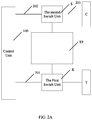
- FIG. 2A shows a schematic touch-control circuit diagram of another exemplary single touch-control electrode consistent with disclosed embodiments.
- a touch-control electrode TP is connected to one terminal of at least one first switch unit K.
- the other terminal of the first switch unit K is electrically connected to a touch-detection terminal T.
- the control terminal of the first switch unit K is electrically connected to a corresponding terminal of a control unit 100 through at least one first control lead 201 .
- the touch-control electrode TP is also electrically connected to one terminal of at least one second switch unit S.
- the other terminal of the second switch unit S is electrically connected to a reference signal terminal C.
- the control terminal of the second switch unit S is electrically connected to a corresponding terminal of a control unit 100 through at least one second control lead 202 .
- the control unit 100 controls the first switch unit K to be in an ON status and the second switch unit S to be in an OFF status. Therefore, the touch-detection terminal T and the touch-control electrode TP are connected, allowing detection on the touch-control electrode TP.
- the control unit 100 controls the first switch unit K to be in an OFF status and the second switch unit S to be in an ON status. Therefore, the connection between the touch-detection terminal T and the touch-control electrode TP is disconnected, and the reference signal sent out from the reference signal terminal C is transmitted to the touch-control electrode TP through the second switch unit S.
- both the first switch unit and the second switch unit may include a switch transistor.
- the first switch unit K includes at least one first-type switch transistor
- the second switch unit S includes at least one second-type switch transistor
- the conductivity type of the first-type switch transistor and the conductivity type of the second-type switch transistor are the same.
- the first switch unit K may include at least one first-type switch transistor
- the second switch unit S may include at least one second-type switch transistor
- the conductivity type of the first-type switch transistor and the conductivity type of the second-type switch transistor are opposite to each other.
- FIG. 2B shows a schematic touch-control circuit diagram of another exemplary single touch-control electrode consistent with disclosed embodiments.
- a first switch unit K includes a first-type switch transistor. One terminal of the first-type switch transistor is electrically connected to the touch-control electrode TP while the other terminal of the first-type switch transistor is electrically connected to a corresponding touch-detection terminal T.
- the control terminal of the first-type switch transistor is electrically connected to a corresponding terminal of the control unit 100 through a first control lead 201 .
- a second switch unit S includes a second-type switch transistor.
- One terminal of the second-type switch transistor is electrically connected to the touch-control electrode TP while the other terminal of the second-type switch transistor is electrically connected to a corresponding reference signal terminal C.
- the control terminal of the second-type switch transistor is electrically connected to a corresponding terminal of the control unit 100 through a second control lead 202 .
- the conductivity type of the first-type switch transistor shown in FIG. 2B and the conductivity type of the second-type switch transistor shown in FIG. 2B are the same.
- the first-type switch transistor and the second-type switch transistor may be both N-type switch transistors, or may be both P-type switch transistors. Therefore, during the wiring process, the first control lead and the second control lead may be respectively connected to the first switch unit and the second switch unit to realize the ON status and the OFF status for each of the two switch units in different phases.
- the type of the first-type switch transistor and the type of the second switch transistor may be opposite to each other to reduce the total number of the control leads. Therefore, the first switch unit and the second switch unit of a given touch-control electrode may be electrically connected to the control unit through a same control lead. That is, for a given touch-control electrode, the first control lead connected to the first switch unit and the second control lead connected to the second switch unit may be a same control lead.
- FIG. 2C shows a schematic touch-control circuit diagram of another exemplary single touch-control electrode consistent with disclosed embodiments.
- the first-type switch transistor is an N-type switch transistor and the second-type switch transistor is a P-type switch transistor.
- the two types of switch transistors may be interchangeable.
- the control terminals of the two types of switch transistors may be connected together by a control lead 201 ( 202 ), which is also electrically connected to a corresponding terminal of the control unit 100 .
- the corresponding terminal of the control unit 100 may send out a high-level signal to control the first-type switch transistor to be in the ON status while having the second-type switch transistor in the OFF status to allow detection on the touch-control electrode TP.
- the corresponding terminal of the control unit 100 may send out a low-level signal to control the first-type switch transistor to be in the OFF status while having the second-type switch transistor in the ON status to transmit the reference signal to the touch-control electrode TP.
- FIG. 2D shows a schematic touch-control circuit diagram of another exemplary single touch-control electrode consistent with disclosed embodiments. Compared to the embodiments shown in FIGS. 2A-2C , where each switch unit only includes one switch transistor, the touch-control circuit diagram shown in FIG. 2D provides an example in which both the first switch unit and the second switch unit may include multiple switch transistors.
- a first switch unit K includes a plurality of first-type switch transistors.
- the plurality of first-type switch transistors may be connected in a series with the two terminals of the series electrically connected to the touch-control electrode TP and the touch-detection terminal T, respectively.
- the second switch unit S may include a plurality of second-type switch transistors.
- the plurality of second-type switch transistors may be connected in parallel with each other with each second-type switch transistor electrically connected to both the touch-control electrode TP and the touch-detection terminal T.
- the reference signal terminal may include a common signal terminal of the array substrate.
- first switch units corresponding to touch-control electrodes arranged in a same column may be electrically connected to a same touch-detection terminal in order to reduce the number of the touch-detection terminals and also reduce the difficulty in arranging the leads.
- the touch-detection terminal may include a data-signal input terminal, i.e., the data-signal input terminal may be a multiplex electrode used also as a touch-detection terminal.
- the second switch unit may be electrically connected to a reference signal terminal through a reference lead 203 to further ensure the aperture ratio of the pixel units.
- the reference lead 203 may be arranged between any pair of neighboring rows of the pixel units.
- There reference lead 203 , the first control lead 201 , and the second control lead 202 may be arranged between different neighboring rows of the pixel units in order to avoid overlay dense wiring between two neighboring rows of the pixel units.
- a reference signal terminal is also a common signal terminal, because the common signal is more important for the display of the display device, the ON-state impedance of the second switch unit for transmitting the common signal may need to be small. Usually, the ON-state impedance of the second switch unit may need to be below 50 k ⁇ . Further, the OFF-state impedance of the first switch unit may need to be relatively large in order to prevent signal crosstalk. Usually, the OFF-state impedance of the first switch unit may need to be above 5000 k ⁇ .
- the type of the switch transistors in the first switch unit and the second switch unit, the connection strategies, and the width to length ratio may not be limited to any specific selections.
- the type of the switch transistors in the first switch unit and the second switch unit, the connection strategies, and the width to length ratio may be defined based on actual requirements.
- FIG. 3A shows a schematic view of an exemplary array substrate consistent with disclosed embodiments.
- FIG. 3B shows a schematic processing diagram for the array substrate shown in FIG. 3A .
- the present disclosure is described to have the array substrate include four touch-control electrodes to illustrate the relation of the plurality of touch-control electrodes and the operation mechanism of the disclosed method, although any number of touch-control electrodes, more or less than four, may be included in the array substrate.
- the first switch units and the second switch units may all have an ON status corresponding to a high-level signal and an OFF status corresponding to a low-level signal.
- the array substrate includes four touch-control electrodes, i.e. a first touch-control electrode 11 , a second touch-control electrode 12 , a third touch-control electrode 13 , and a fourth touch-control electrode 14 .
- the first touch-control electrode 11 is electrically connected to a terminal of the first switch unit K 1
- the second touch-control electrode 12 is electrically connected to a terminal of the first switch unit K 2
- the third touch-control electrode 13 is electrically connected to a terminal of the first switch unit K 3
- the fourth touch-control electrode 14 is electrically connected to a terminal of the first switch unit K 4 .
- the other terminal of the first switch unit K 1 and the other terminal of the first switch unit K 3 are electrically connected to a same touch-detection terminal T 1 while the control terminals of the first switch units K 1 and K 2 are electrically connected to a same terminal of the control unit 100 through a first control lead 201 .
- the other terminal of the first switch unit K 2 and the other terminal of the first switch unit K 4 are electrically connected to a same touch-detection terminal T 2 while the control terminals of the first switch units K 1 and K 2 are electrically connected to a same terminal of the control unit 100 through a first control lead 201 .
- the first control lead 201 may be arranged between two neighboring rows of the pixel units.
- first touch-control electrode 11 is electrically connected to a terminal of the second switch unit S 1
- the second touch-control electrode 12 is electrically connected to a terminal of the second switch unit S 2
- the third touch-control electrode 13 is electrically connected to a terminal of the third switch unit S 3
- the fourth touch-control electrode 14 is electrically connected to a terminal of the second switch unit S 4 .
- the other terminals of the first touch-control electrode 11 , the second touch-control electrode 12 , the third touch-control electrode 13 , and the fourth touch-control electrode 1 are electrically connected to a reference signal terminal C.
- the control terminals of the first switch units S 1 and S 2 are electrically connected to a corresponding control unit 100 through a second control lead 202 .
- the control terminals of the second switch units S 3 and S 4 are also electrically connected to a corresponding control unit 100 through a second control lead 202 .
- the second control lead 202 may be arranged between two neighboring rows of the pixel units.
- the control unit 100 may first send out high-level signals to the first switch units K 1 and K 2 and low-level signals to the first switch units K 3 and K 4 as well as the second switch units S 1 , S 2 , S 3 , and S 4 . That is, the control unit 100 may control the first switch units K 1 and K 2 in the ON status while controlling the first switch units K 3 and K 4 as well as the second switch units S 1 , S 2 , S 3 , and S 4 in the OFF status.
- the touch-detection terminal T 1 and the first touch-control electrode 11 are electrically connected to allow the detection on the first touch-control electrode 11 , and in the meantime, the touch-detection terminal T 2 and the second touch-control electrode 12 are also electrically connected to allow the detection on the second touch-control electrode 12 .
- the control unit 100 may then send out high-level signals to the first switch units K 3 and K 4 and low-level signals to the first switch units K 1 and K 2 as well as the second switch units S 1 , S 2 , S 3 , and S 4 . That is, the control unit 100 may control the first switch units K 3 and K 4 to be in the ON status while controlling the first switch units K 1 and K 2 as well as the second switch units S 1 , S 2 , S 3 , and S 4 to be in the OFF status.
- the touch-detection terminal T 3 and the third touch-control electrode 13 are electrically connected to allow the detection on the third touch-control electrode 13 , and in the meantime, the touch-detection terminal T 4 and the fourth touch-control electrode 14 are also electrically connected to allow the detection on the fourth touch-control electrode 14 .
- control unit may sequentially control all the first switch units to be in the ON status while having all the second switch units in the OFF status to realize line-by-line control of touch detection for multiple touch-control electrodes.
- the control unit 100 may send out low-level signals to all the first switch units K 1 , K 2 , K 3 , and K 4 , and in the meantime, send out high-level signals to all the second switch units S 1 , S 2 , S 3 , and S 4 . That is, the control unit 100 may have all the first switch units K 1 , K 2 , K 3 , and K 4 in the OFF status while having all the second switch units S 1 , S 2 , S 3 , and S 4 in the ON status to transmit reference signals at the reference signal terminals to the first touch-control electrode 11 , the second touch-control electrode 12 , the third touch-control electrode 13 , and the fourth touch-control electrode 14 .
- FIG. 3C shows a schematic view of the detailed structure of region D shown in FIG. 3A .
- a first control lead is described herein as an example.
- the first control lead 201 may be formed between two neighboring rows of pixel units.
- the first switch unit K 1 is a switch transistor.
- the gate electrode of the switch transistor may be electrically connected to the first control lead 201 .
- One terminal of the switch transistor may be electrically connected to the corresponding touch-detection terminal T 1 while the other terminal of the switch transistor may be electrically connected to the first touch-control electrode 11 .
- arranging the first control lead between neighboring rows of pixel units may avoid affecting the aperture ratio of the pixel units, thus ensure high display quality of the display device.
- the first control lead 201 may or may not be arranged in a same conductive layer as the gate electrode.
- FIG. 4 shows a schematic view of an exemplary display panel consistent with disclosed embodiments.
- the display panel includes an array substrate 10 consistent with above disclosed embodiments, and a first substrate 20 disposed corresponding to the array substrate.
- the first substrate may be a color film substrate.
- the display panel may also include a liquid crystal layer 30 between the first substrate 20 and the array substrate 10 .
- the type of the first substrate may be any appropriate substrate for forming a display panel.
- FIG. 5 shows a schematic view of an exemplary display device consistent with disclosed embodiments.
- the display device includes a display panel consistent with above disclosed embodiments.
- the display device may be a liquid crystal display device.
- the display device may include a display panel 301 consistent with above disclosed embodiments.
- the display device may also include a backlight module 302 disposed corresponding to the display panel 301 .
- the display device may also be an organic light-emitting diode (OLED) display device or other type of display device.
- OLED organic light-emitting diode
- an array substrate, a display panel, and a display device are provided.
- the array substrate includes a plurality of gate electrode lines and a plurality of data lines.
- the plurality of gate electrode lines intercept with the plurality of data lines to define an array for a plurality of pixel units.
- the array substrate may also include a touch-control circuit and a plurality of touch-control electrodes arranged in an array.
- the plurality of touch-control electrodes may be independent from each other.
- the touch-control circuit may also include a plurality of first switch units, a plurality of first control leads, a plurality of touch-detection terminals and a control unit.
- Each touch-control electrode may be electrically connected to a touch-detection terminal through at least one of the first switch units while each first switch unit may be electrically connected to the control unit through at least one of the first control leads.
- the first control leads may be arranged between any pair of neighboring rows of pixel units.
- the control unit may sequentially control the first switch units to be in an ON status to allow line-by-line control of touch detection for the plurality of touch-control electrodes.
- the array substrate may be adopted in a display panel and the display panel may further by used in a display device.
- the touch-control structure on the array substrate may be simple and clear, and the area occupied by the touch-control structure may also be relatively small. Therefore, the disclosed array substrate, display panel, and display device may conducive to the development of thinner and lighter display devices.
- the aperture ratio of the pixel units may not be affected, thus high display quality of the display device may be ensured.
Landscapes
- Engineering & Computer Science (AREA)
- General Engineering & Computer Science (AREA)
- Theoretical Computer Science (AREA)
- Human Computer Interaction (AREA)
- Physics & Mathematics (AREA)
- General Physics & Mathematics (AREA)
- Devices For Indicating Variable Information By Combining Individual Elements (AREA)
- Position Input By Displaying (AREA)
- Liquid Crystal (AREA)
Abstract
Description
Claims (20)
Priority Applications (1)
| Application Number | Priority Date | Filing Date | Title |
|---|---|---|---|
| DE102016117303.7A DE102016117303A1 (en) | 2015-12-11 | 2016-09-14 | ARRAY SUBSTRATE, DISPLAY PANEL, DISPLAY DEVICE AND METHOD FOR THE PRODUCTION THEREOF |
Applications Claiming Priority (3)
| Application Number | Priority Date | Filing Date | Title |
|---|---|---|---|
| CN2015-10926109.2 | 2015-12-11 | ||
| CN201510926109 | 2015-12-11 | ||
| CN201510926109.2A CN105373259B (en) | 2015-12-11 | 2015-12-11 | A kind of array substrate, display panel and display device |
Publications (2)
| Publication Number | Publication Date |
|---|---|
| US20170168636A1 US20170168636A1 (en) | 2017-06-15 |
| US10551956B2 true US10551956B2 (en) | 2020-02-04 |
Family
ID=55375520
Family Applications (1)
| Application Number | Title | Priority Date | Filing Date |
|---|---|---|---|
| US15/163,397 Active 2037-02-12 US10551956B2 (en) | 2015-12-11 | 2016-05-24 | Array substrate, display panel, display device, and fabrication method thereof |
Country Status (2)
| Country | Link |
|---|---|
| US (1) | US10551956B2 (en) |
| CN (1) | CN105373259B (en) |
Families Citing this family (11)
| Publication number | Priority date | Publication date | Assignee | Title |
|---|---|---|---|---|
| DE102016117303A1 (en) | 2015-12-11 | 2017-06-14 | Shanghai Avic Opto Electronics Co. Ltd | ARRAY SUBSTRATE, DISPLAY PANEL, DISPLAY DEVICE AND METHOD FOR THE PRODUCTION THEREOF |
| CN106708344A (en) * | 2017-01-03 | 2017-05-24 | 京东方科技集团股份有限公司 | Touch panel, driving method for touch panel, and touch screen |
| CN107506083B (en) * | 2017-09-01 | 2020-09-18 | 厦门天马微电子有限公司 | Display panel, pressure testing method thereof and display device |
| US10861513B2 (en) * | 2018-10-31 | 2020-12-08 | Taiwan Semiconductor Manufacturing Company, Ltd. | Memory device with selective precharging |
| CN109614010B (en) * | 2019-01-09 | 2023-10-13 | 深圳市德明利技术股份有限公司 | Touch screen and electronic equipment |
| CN110716665B (en) | 2019-09-30 | 2021-09-17 | 厦门天马微电子有限公司 | Touch display panel and display device |
| CN111582103B (en) * | 2020-04-28 | 2024-04-12 | 上海天马微电子有限公司 | Fingerprint identification structure, device, display panel and display device |
| CN112860110B (en) * | 2021-02-09 | 2023-12-15 | 武汉华星光电半导体显示技术有限公司 | Touch display panel |
| CN113514673B (en) * | 2021-09-14 | 2022-01-28 | 苏州华兴源创科技股份有限公司 | Touch channel switching circuit, device and detection system |
| CN114167254B (en) * | 2021-10-31 | 2023-12-12 | 重庆台冠科技有限公司 | First TP testing tool and TP testing device |
| CN119916963B (en) * | 2024-12-31 | 2025-09-26 | 合肥维信诺科技有限公司 | Display panel and display device |
Citations (14)
| Publication number | Priority date | Publication date | Assignee | Title |
|---|---|---|---|---|
| US20040135951A1 (en) * | 2002-09-30 | 2004-07-15 | Dave Stumbo | Integrated displays using nanowire transistors |
| US20100231493A1 (en) * | 2007-09-27 | 2010-09-16 | Yasuyoshi Kaise | Display device |
| US20110050585A1 (en) * | 2009-08-25 | 2011-03-03 | Steven Porter Hotelling | Integrated touch screen |
| US20120218199A1 (en) * | 2011-02-25 | 2012-08-30 | Kim Cheolse | Touch sensor integrated display device |
| CN102693034A (en) | 2010-12-23 | 2012-09-26 | 韩国电子通信研究院 | Touch input device and electromagnetic-wave transceiver using the same device |
| US20120249444A1 (en) * | 2011-04-01 | 2012-10-04 | Lg Display Co., Ltd. | Touch Sensor Integrated Type Display Device |
| US20140152619A1 (en) * | 2006-06-09 | 2014-06-05 | Apple Inc. | Touch screen liquid crystal display |
| US20140168157A1 (en) * | 2012-12-13 | 2014-06-19 | Beijing Boe Optoelectronics Technology Co., Ltd. | Touch display circuit, drive method thereof, array substrate and display device |
| US20140168127A1 (en) * | 2012-12-18 | 2014-06-19 | Beijing Boe Optoelectronics Technology Co., Ltd. | Touch display circuit and driving method thereof, array substrate and display apparatus |
| US20150097808A1 (en) * | 2013-10-04 | 2015-04-09 | Samsung Display Co., Ltd. | Touch screen display |
| CN104699347A (en) | 2015-04-01 | 2015-06-10 | 上海中航光电子有限公司 | Array substrate, display panel and electronic equipment |
| CN104765498A (en) | 2015-04-13 | 2015-07-08 | 业成光电(深圳)有限公司 | Touch display panel |
| CN105301822A (en) | 2015-12-11 | 2016-02-03 | 上海中航光电子有限公司 | Array substrate, display panel and display device |
| US20160188040A1 (en) * | 2014-12-26 | 2016-06-30 | Lg Display Co., Ltd. | Touch Sensor Integrated Type Display Device |
Family Cites Families (2)
| Publication number | Priority date | Publication date | Assignee | Title |
|---|---|---|---|---|
| US6865191B1 (en) * | 1999-08-12 | 2005-03-08 | Telefonaktiebolaget Lm Ericsson (Publ) | System and method for sending multimedia attachments to text messages in radiocommunication systems |
| CN105068694B (en) * | 2015-09-07 | 2018-01-26 | 上海天马微电子有限公司 | Touch display panel and driving method thereof |
-
2015
- 2015-12-11 CN CN201510926109.2A patent/CN105373259B/en not_active Expired - Fee Related
-
2016
- 2016-05-24 US US15/163,397 patent/US10551956B2/en active Active
Patent Citations (14)
| Publication number | Priority date | Publication date | Assignee | Title |
|---|---|---|---|---|
| US20040135951A1 (en) * | 2002-09-30 | 2004-07-15 | Dave Stumbo | Integrated displays using nanowire transistors |
| US20140152619A1 (en) * | 2006-06-09 | 2014-06-05 | Apple Inc. | Touch screen liquid crystal display |
| US20100231493A1 (en) * | 2007-09-27 | 2010-09-16 | Yasuyoshi Kaise | Display device |
| US20110050585A1 (en) * | 2009-08-25 | 2011-03-03 | Steven Porter Hotelling | Integrated touch screen |
| CN102693034A (en) | 2010-12-23 | 2012-09-26 | 韩国电子通信研究院 | Touch input device and electromagnetic-wave transceiver using the same device |
| US20120218199A1 (en) * | 2011-02-25 | 2012-08-30 | Kim Cheolse | Touch sensor integrated display device |
| US20120249444A1 (en) * | 2011-04-01 | 2012-10-04 | Lg Display Co., Ltd. | Touch Sensor Integrated Type Display Device |
| US20140168157A1 (en) * | 2012-12-13 | 2014-06-19 | Beijing Boe Optoelectronics Technology Co., Ltd. | Touch display circuit, drive method thereof, array substrate and display device |
| US20140168127A1 (en) * | 2012-12-18 | 2014-06-19 | Beijing Boe Optoelectronics Technology Co., Ltd. | Touch display circuit and driving method thereof, array substrate and display apparatus |
| US20150097808A1 (en) * | 2013-10-04 | 2015-04-09 | Samsung Display Co., Ltd. | Touch screen display |
| US20160188040A1 (en) * | 2014-12-26 | 2016-06-30 | Lg Display Co., Ltd. | Touch Sensor Integrated Type Display Device |
| CN104699347A (en) | 2015-04-01 | 2015-06-10 | 上海中航光电子有限公司 | Array substrate, display panel and electronic equipment |
| CN104765498A (en) | 2015-04-13 | 2015-07-08 | 业成光电(深圳)有限公司 | Touch display panel |
| CN105301822A (en) | 2015-12-11 | 2016-02-03 | 上海中航光电子有限公司 | Array substrate, display panel and display device |
Also Published As
| Publication number | Publication date |
|---|---|
| CN105373259A (en) | 2016-03-02 |
| CN105373259B (en) | 2018-11-27 |
| US20170168636A1 (en) | 2017-06-15 |
Similar Documents
| Publication | Publication Date | Title |
|---|---|---|
| US10551956B2 (en) | Array substrate, display panel, display device, and fabrication method thereof | |
| US9740355B2 (en) | Self-capacitive touch display panel, array substrate therefor and touch device | |
| US20170192558A1 (en) | Array substrate, touch display panel and touch display device | |
| CN105301822B (en) | A kind of array substrate, display panel and display device | |
| US11139317B2 (en) | Array substrate, touch panel and manufacturing method of array substrate | |
| US10268304B2 (en) | Touch display panel, manufacturing method for the same, driving method for the same, and display device | |
| US9703440B2 (en) | Self-capacitive touch display panel and array substrate thereof | |
| CN104536632B (en) | A kind of In-cell touch panel and display device | |
| US10241606B2 (en) | Display device | |
| US9690416B2 (en) | Touch panel, touch display panel and touch detection and display method | |
| US10013105B2 (en) | Touch display device | |
| US10635244B2 (en) | Head mounted display device and fabricating method thereof | |
| US9836159B2 (en) | Touch display panel and method for driving the same | |
| US20170177158A1 (en) | Touch control display panel and touch control display device | |
| US9881537B2 (en) | Display panel and flat panel display apparatus with transmission lines for connecting gate lines to control circuit | |
| KR20180038603A (en) | Touch screen and display device having the same | |
| US10025416B2 (en) | Display panel and method for forming the same | |
| US10748940B2 (en) | TFT substrate having data lines as touch driving electrode and common electrodes as touch sensing electrode and touch display panel using same | |
| CN110007806A (en) | Display device | |
| US20160328059A1 (en) | In-Cell Touch Screen and Display Device | |
| CN110688030A (en) | Touch display panel and display device | |
| KR20170088010A (en) | Display device | |
| KR20170080314A (en) | Display device including touch panel | |
| US11231795B2 (en) | Touch control array substrate having a plurality of auxiliary conductive lines, and display apparatus thereof | |
| CN116700519B (en) | Touch display panel, driving method and touch display device |
Legal Events
| Date | Code | Title | Description |
|---|---|---|---|
| AS | Assignment |
Owner name: SHANGHAI AVIC OPTO ELECTRONICS CO., LTD., CHINA Free format text: ASSIGNMENT OF ASSIGNORS INTEREST;ASSIGNORS:XI, KERUI;CUI, TINGTING;REEL/FRAME:038707/0269 Effective date: 20160518 Owner name: TIANMA MICRO-ELECTRONICS CO., LTD., CHINA Free format text: ASSIGNMENT OF ASSIGNORS INTEREST;ASSIGNORS:XI, KERUI;CUI, TINGTING;REEL/FRAME:038707/0269 Effective date: 20160518 |
|
| STPP | Information on status: patent application and granting procedure in general |
Free format text: DOCKETED NEW CASE - READY FOR EXAMINATION |
|
| STPP | Information on status: patent application and granting procedure in general |
Free format text: NON FINAL ACTION MAILED |
|
| STPP | Information on status: patent application and granting procedure in general |
Free format text: RESPONSE TO NON-FINAL OFFICE ACTION ENTERED AND FORWARDED TO EXAMINER |
|
| STPP | Information on status: patent application and granting procedure in general |
Free format text: FINAL REJECTION MAILED |
|
| STPP | Information on status: patent application and granting procedure in general |
Free format text: NOTICE OF ALLOWANCE MAILED -- APPLICATION RECEIVED IN OFFICE OF PUBLICATIONS |
|
| STPP | Information on status: patent application and granting procedure in general |
Free format text: PUBLICATIONS -- ISSUE FEE PAYMENT VERIFIED |
|
| STCF | Information on status: patent grant |
Free format text: PATENTED CASE |
|
| MAFP | Maintenance fee payment |
Free format text: PAYMENT OF MAINTENANCE FEE, 4TH YEAR, LARGE ENTITY (ORIGINAL EVENT CODE: M1551); ENTITY STATUS OF PATENT OWNER: LARGE ENTITY Year of fee payment: 4 |