US10547152B2 - Electrical connector assembly method - Google Patents
Electrical connector assembly method Download PDFInfo
- Publication number
- US10547152B2 US10547152B2 US15/869,709 US201815869709A US10547152B2 US 10547152 B2 US10547152 B2 US 10547152B2 US 201815869709 A US201815869709 A US 201815869709A US 10547152 B2 US10547152 B2 US 10547152B2
- Authority
- US
- United States
- Prior art keywords
- solder
- soldering portion
- electrical connector
- width
- assembly method
- Prior art date
- Legal status (The legal status is an assumption and is not a legal conclusion. Google has not performed a legal analysis and makes no representation as to the accuracy of the status listed.)
- Active, expires
Links
Images


Classifications
-
- H—ELECTRICITY
- H01—ELECTRIC ELEMENTS
- H01R—ELECTRICALLY-CONDUCTIVE CONNECTIONS; STRUCTURAL ASSOCIATIONS OF A PLURALITY OF MUTUALLY-INSULATED ELECTRICAL CONNECTING ELEMENTS; COUPLING DEVICES; CURRENT COLLECTORS
- H01R43/00—Apparatus or processes specially adapted for manufacturing, assembling, maintaining, or repairing of line connectors or current collectors or for joining electric conductors
- H01R43/02—Apparatus or processes specially adapted for manufacturing, assembling, maintaining, or repairing of line connectors or current collectors or for joining electric conductors for soldered or welded connections
- H01R43/0263—Apparatus or processes specially adapted for manufacturing, assembling, maintaining, or repairing of line connectors or current collectors or for joining electric conductors for soldered or welded connections for positioning or holding parts during soldering or welding process
-
- H—ELECTRICITY
- H01—ELECTRIC ELEMENTS
- H01R—ELECTRICALLY-CONDUCTIVE CONNECTIONS; STRUCTURAL ASSOCIATIONS OF A PLURALITY OF MUTUALLY-INSULATED ELECTRICAL CONNECTING ELEMENTS; COUPLING DEVICES; CURRENT COLLECTORS
- H01R43/00—Apparatus or processes specially adapted for manufacturing, assembling, maintaining, or repairing of line connectors or current collectors or for joining electric conductors
- H01R43/20—Apparatus or processes specially adapted for manufacturing, assembling, maintaining, or repairing of line connectors or current collectors or for joining electric conductors for assembling or disassembling contact members with insulating base, case or sleeve
- H01R43/24—Assembling by moulding on contact members
-
- B—PERFORMING OPERATIONS; TRANSPORTING
- B23—MACHINE TOOLS; METAL-WORKING NOT OTHERWISE PROVIDED FOR
- B23K—SOLDERING OR UNSOLDERING; WELDING; CLADDING OR PLATING BY SOLDERING OR WELDING; CUTTING BY APPLYING HEAT LOCALLY, e.g. FLAME CUTTING; WORKING BY LASER BEAM
- B23K1/00—Soldering, e.g. brazing, or unsoldering
- B23K1/0008—Soldering, e.g. brazing, or unsoldering specially adapted for particular articles or work
- B23K1/0016—Soldering of electronic components
-
- B—PERFORMING OPERATIONS; TRANSPORTING
- B23—MACHINE TOOLS; METAL-WORKING NOT OTHERWISE PROVIDED FOR
- B23K—SOLDERING OR UNSOLDERING; WELDING; CLADDING OR PLATING BY SOLDERING OR WELDING; CUTTING BY APPLYING HEAT LOCALLY, e.g. FLAME CUTTING; WORKING BY LASER BEAM
- B23K1/00—Soldering, e.g. brazing, or unsoldering
- B23K1/002—Soldering by means of induction heating
-
- B—PERFORMING OPERATIONS; TRANSPORTING
- B23—MACHINE TOOLS; METAL-WORKING NOT OTHERWISE PROVIDED FOR
- B23K—SOLDERING OR UNSOLDERING; WELDING; CLADDING OR PLATING BY SOLDERING OR WELDING; CUTTING BY APPLYING HEAT LOCALLY, e.g. FLAME CUTTING; WORKING BY LASER BEAM
- B23K1/00—Soldering, e.g. brazing, or unsoldering
- B23K1/20—Preliminary treatment of work or areas to be soldered, e.g. in respect of a galvanic coating
-
- H—ELECTRICITY
- H01—ELECTRIC ELEMENTS
- H01R—ELECTRICALLY-CONDUCTIVE CONNECTIONS; STRUCTURAL ASSOCIATIONS OF A PLURALITY OF MUTUALLY-INSULATED ELECTRICAL CONNECTING ELEMENTS; COUPLING DEVICES; CURRENT COLLECTORS
- H01R12/00—Structural associations of a plurality of mutually-insulated electrical connecting elements, specially adapted for printed circuits, e.g. printed circuit boards [PCB], flat or ribbon cables, or like generally planar structures, e.g. terminal strips, terminal blocks; Coupling devices specially adapted for printed circuits, flat or ribbon cables, or like generally planar structures; Terminals specially adapted for contact with, or insertion into, printed circuits, flat or ribbon cables, or like generally planar structures
- H01R12/50—Fixed connections
- H01R12/51—Fixed connections for rigid printed circuits or like structures
- H01R12/55—Fixed connections for rigid printed circuits or like structures characterised by the terminals
- H01R12/57—Fixed connections for rigid printed circuits or like structures characterised by the terminals surface mounting terminals
-
- H—ELECTRICITY
- H01—ELECTRIC ELEMENTS
- H01R—ELECTRICALLY-CONDUCTIVE CONNECTIONS; STRUCTURAL ASSOCIATIONS OF A PLURALITY OF MUTUALLY-INSULATED ELECTRICAL CONNECTING ELEMENTS; COUPLING DEVICES; CURRENT COLLECTORS
- H01R12/00—Structural associations of a plurality of mutually-insulated electrical connecting elements, specially adapted for printed circuits, e.g. printed circuit boards [PCB], flat or ribbon cables, or like generally planar structures, e.g. terminal strips, terminal blocks; Coupling devices specially adapted for printed circuits, flat or ribbon cables, or like generally planar structures; Terminals specially adapted for contact with, or insertion into, printed circuits, flat or ribbon cables, or like generally planar structures
- H01R12/50—Fixed connections
- H01R12/51—Fixed connections for rigid printed circuits or like structures
- H01R12/55—Fixed connections for rigid printed circuits or like structures characterised by the terminals
- H01R12/58—Fixed connections for rigid printed circuits or like structures characterised by the terminals terminals for insertion into holes
- H01R12/585—Terminals having a press fit or a compliant portion and a shank passing through a hole in the printed circuit board
-
- H—ELECTRICITY
- H01—ELECTRIC ELEMENTS
- H01R—ELECTRICALLY-CONDUCTIVE CONNECTIONS; STRUCTURAL ASSOCIATIONS OF A PLURALITY OF MUTUALLY-INSULATED ELECTRICAL CONNECTING ELEMENTS; COUPLING DEVICES; CURRENT COLLECTORS
- H01R12/00—Structural associations of a plurality of mutually-insulated electrical connecting elements, specially adapted for printed circuits, e.g. printed circuit boards [PCB], flat or ribbon cables, or like generally planar structures, e.g. terminal strips, terminal blocks; Coupling devices specially adapted for printed circuits, flat or ribbon cables, or like generally planar structures; Terminals specially adapted for contact with, or insertion into, printed circuits, flat or ribbon cables, or like generally planar structures
- H01R12/70—Coupling devices
- H01R12/7005—Guiding, mounting, polarizing or locking means; Extractors
- H01R12/7011—Locking or fixing a connector to a PCB
- H01R12/707—Soldering or welding
-
- H—ELECTRICITY
- H01—ELECTRIC ELEMENTS
- H01R—ELECTRICALLY-CONDUCTIVE CONNECTIONS; STRUCTURAL ASSOCIATIONS OF A PLURALITY OF MUTUALLY-INSULATED ELECTRICAL CONNECTING ELEMENTS; COUPLING DEVICES; CURRENT COLLECTORS
- H01R4/00—Electrically-conductive connections between two or more conductive members in direct contact, i.e. touching one another; Means for effecting or maintaining such contact; Electrically-conductive connections having two or more spaced connecting locations for conductors and using contact members penetrating insulation
- H01R4/02—Soldered or welded connections
- H01R4/023—Soldered or welded connections between cables or wires and terminals
- H01R4/024—Soldered or welded connections between cables or wires and terminals comprising preapplied solder
-
- H—ELECTRICITY
- H01—ELECTRIC ELEMENTS
- H01R—ELECTRICALLY-CONDUCTIVE CONNECTIONS; STRUCTURAL ASSOCIATIONS OF A PLURALITY OF MUTUALLY-INSULATED ELECTRICAL CONNECTING ELEMENTS; COUPLING DEVICES; CURRENT COLLECTORS
- H01R43/00—Apparatus or processes specially adapted for manufacturing, assembling, maintaining, or repairing of line connectors or current collectors or for joining electric conductors
- H01R43/20—Apparatus or processes specially adapted for manufacturing, assembling, maintaining, or repairing of line connectors or current collectors or for joining electric conductors for assembling or disassembling contact members with insulating base, case or sleeve
- H01R43/205—Apparatus or processes specially adapted for manufacturing, assembling, maintaining, or repairing of line connectors or current collectors or for joining electric conductors for assembling or disassembling contact members with insulating base, case or sleeve with a panel or printed circuit board
-
- H—ELECTRICITY
- H05—ELECTRIC TECHNIQUES NOT OTHERWISE PROVIDED FOR
- H05K—PRINTED CIRCUITS; CASINGS OR CONSTRUCTIONAL DETAILS OF ELECTRIC APPARATUS; MANUFACTURE OF ASSEMBLAGES OF ELECTRICAL COMPONENTS
- H05K3/00—Apparatus or processes for manufacturing printed circuits
- H05K3/30—Assembling printed circuits with electric components, e.g. with resistors
- H05K3/32—Assembling printed circuits with electric components, e.g. with resistors electrically connecting electric components or wires to printed circuits
- H05K3/34—Assembling printed circuits with electric components, e.g. with resistors electrically connecting electric components or wires to printed circuits by soldering
- H05K3/341—Surface mounted components
- H05K3/3421—Leaded components
- H05K3/3426—Leaded components characterised by the leads
-
- H—ELECTRICITY
- H01—ELECTRIC ELEMENTS
- H01R—ELECTRICALLY-CONDUCTIVE CONNECTIONS; STRUCTURAL ASSOCIATIONS OF A PLURALITY OF MUTUALLY-INSULATED ELECTRICAL CONNECTING ELEMENTS; COUPLING DEVICES; CURRENT COLLECTORS
- H01R12/00—Structural associations of a plurality of mutually-insulated electrical connecting elements, specially adapted for printed circuits, e.g. printed circuit boards [PCB], flat or ribbon cables, or like generally planar structures, e.g. terminal strips, terminal blocks; Coupling devices specially adapted for printed circuits, flat or ribbon cables, or like generally planar structures; Terminals specially adapted for contact with, or insertion into, printed circuits, flat or ribbon cables, or like generally planar structures
- H01R12/70—Coupling devices
- H01R12/7082—Coupling device supported only by cooperation with PCB
-
- H—ELECTRICITY
- H05—ELECTRIC TECHNIQUES NOT OTHERWISE PROVIDED FOR
- H05K—PRINTED CIRCUITS; CASINGS OR CONSTRUCTIONAL DETAILS OF ELECTRIC APPARATUS; MANUFACTURE OF ASSEMBLAGES OF ELECTRICAL COMPONENTS
- H05K1/00—Printed circuits
- H05K1/02—Details
- H05K1/11—Printed elements for providing electric connections to or between printed circuits
- H05K1/111—Pads for surface mounting, e.g. lay-out
-
- H—ELECTRICITY
- H05—ELECTRIC TECHNIQUES NOT OTHERWISE PROVIDED FOR
- H05K—PRINTED CIRCUITS; CASINGS OR CONSTRUCTIONAL DETAILS OF ELECTRIC APPARATUS; MANUFACTURE OF ASSEMBLAGES OF ELECTRICAL COMPONENTS
- H05K2201/00—Indexing scheme relating to printed circuits covered by H05K1/00
- H05K2201/09—Shape and layout
- H05K2201/09209—Shape and layout details of conductors
- H05K2201/09372—Pads and lands
- H05K2201/09472—Recessed pad for surface mounting; Recessed electrode of component
-
- H—ELECTRICITY
- H05—ELECTRIC TECHNIQUES NOT OTHERWISE PROVIDED FOR
- H05K—PRINTED CIRCUITS; CASINGS OR CONSTRUCTIONAL DETAILS OF ELECTRIC APPARATUS; MANUFACTURE OF ASSEMBLAGES OF ELECTRICAL COMPONENTS
- H05K2201/00—Indexing scheme relating to printed circuits covered by H05K1/00
- H05K2201/10—Details of components or other objects attached to or integrated in a printed circuit board
- H05K2201/10227—Other objects, e.g. metallic pieces
- H05K2201/10295—Metallic connector elements partly mounted in a hole of the PCB
-
- H—ELECTRICITY
- H05—ELECTRIC TECHNIQUES NOT OTHERWISE PROVIDED FOR
- H05K—PRINTED CIRCUITS; CASINGS OR CONSTRUCTIONAL DETAILS OF ELECTRIC APPARATUS; MANUFACTURE OF ASSEMBLAGES OF ELECTRICAL COMPONENTS
- H05K3/00—Apparatus or processes for manufacturing printed circuits
- H05K3/30—Assembling printed circuits with electric components, e.g. with resistors
- H05K3/32—Assembling printed circuits with electric components, e.g. with resistors electrically connecting electric components or wires to printed circuits
- H05K3/34—Assembling printed circuits with electric components, e.g. with resistors electrically connecting electric components or wires to printed circuits by soldering
-
- Y—GENERAL TAGGING OF NEW TECHNOLOGICAL DEVELOPMENTS; GENERAL TAGGING OF CROSS-SECTIONAL TECHNOLOGIES SPANNING OVER SEVERAL SECTIONS OF THE IPC; TECHNICAL SUBJECTS COVERED BY FORMER USPC CROSS-REFERENCE ART COLLECTIONS [XRACs] AND DIGESTS
- Y02—TECHNOLOGIES OR APPLICATIONS FOR MITIGATION OR ADAPTATION AGAINST CLIMATE CHANGE
- Y02P—CLIMATE CHANGE MITIGATION TECHNOLOGIES IN THE PRODUCTION OR PROCESSING OF GOODS
- Y02P70/00—Climate change mitigation technologies in the production process for final industrial or consumer products
- Y02P70/50—Manufacturing or production processes characterised by the final manufactured product
Definitions
- the present invention relates to an electrical connector assembly method, and particularly to an electrical connector assembly method that can reduce thermal energy needed for soldering a solder and a terminal.
- an electrical connector is located between a chip module and a circuit board for electrically connecting the chip module and the circuit board, and generally includes an insulating body, and conducting terminals accommodated in the insulating body. Each conducting terminal urges upward against the chip module, and urges downward against the circuit board, so as to implement signal transmission between the chip module and the circuit board.
- solder is usually disposed between a soldering portion of the conducting terminal and the circuit board, so that the solder implements the electrical connection between the soldering portion and a gasket of the circuit board.
- the soldering portion and the solder are generally fixed by means of heating, and the solder is pre-soldered and fixed on the soldering portion.
- the so-called pre-soldering is generally performed as follows: each conducting terminal is assembled into an insulating body, and the solder is in contact with the soldering portion by a tool for positioning the solder. Then the insulating body, the conducting terminals, the solder and the positioning tool are altogether placed in a heating apparatus for pre-soldering.
- an objective of the present invention is directed to an electrical connector assembly method that reduces the production cost.
- one aspect of the invention provides an electrical connector assembly method, which includes the following steps: step 1: providing a terminal having a soldering portion; step 2: heating the soldering portion to a melting temperature of a solder; step 3: providing the solder, and press-fitting the solder to the soldering portion by a jig, so that the solder is fused and fixed to the soldering portion; and step 4: inserting the terminal fixed with the solder into an insulating body.
- step 2 the soldering portion is heated by high-frequency current induction, and the solder is press-fit to the soldering portion within 15 seconds after the soldering portion is stopped from being heating.
- the soldering portion is in a vertical flat plate shape, the solder is located at a side of a plate surface of the soldering portion, and a bottom surface of the solder is lower than a bottom surface of the soldering portion.
- the solder is a cuboid shape, and the solder and the soldering portion are laminated face to face.
- a width of the soldering portion is less than a width of the solder.
- a width of the soldering portion is greater than a width of the solder.
- a base portion is formed by extending upward vertically from the soldering portion, a first arm is formed by bending away from a vertical plane of the base portion and extending upward from the base portion, a second arm is formed by bending reversely and extending upward from the first arm and crossing the vertical plane of the base portion, and the first arm and the solder are located at a same side of the vertical plane of the base portion.
- the insulating body has a plurality of accommodating holes vertically running through the insulating body; each of the accommodating holes has a retaining slot for retaining the base portion, and is provided with an accommodating slot at one side of the soldering portion for accommodating the solder; the accommodating slot and the retaining slot communicate with each other; a width of the retaining slot is greater than a width of the accommodating slot; and each of the accommodating holes is provided with a reserved slot at an opposite side of the soldering portion, wherein when press-fitting the solder from the one side of the soldering portion, the reserved slot provides a deformation space to the soldering portion.
- a width of the base portion is greater than a width of the soldering portion, and the base portion is provided with a barrier layer preventing from siphoning and being located higher than the solder.
- a height of the solder is reduced by more than 0.3 millimeters compared with that before the solder is soldered to the circuit board.
- the electrical connector assembly method according to certain embodiments of the invention has the following beneficial effects.
- a soldering portion of a terminal is heated to a melting temperature of a solder, and then the solder is press-fit to the soldering portion by a jig, so that the solder is fused and fixed to the soldering portion. Because only the soldering portion of the terminal is heated, less thermal energy is needed, thereby saving energy and reducing the production cost of the electrical connector. Moreover, the insulating body does not need to be heated, thus preventing the insulating body from being warped and deformed due to heat.
- FIG. 1 is a perspective sectional view of an electrical connector according to a first embodiment of the present invention
- FIG. 2 is a perspective sectional view of the electrical connector in another viewing angle according to the first embodiment of the present invention
- FIG. 3 is a schematic view of press-fitting between a solder and a soldering portion of the electrical connector according to the first embodiment of the present invention
- FIG. 4 is a plain sectional view of the electrical connector being located between a chip module and a circuit board and the chip module being not pressed downward according to the first embodiment of the present invention
- FIG. 5 is a plain sectional view of the electrical connector being located between a chip module and a circuit board and the chip module being pressed downward according to the first embodiment of the present invention
- FIG. 6 is a perspective sectional view of an electrical connector according to a second embodiment of the present invention.
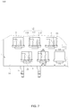
- FIG. 7 is a plain view of the electrical connector according to the second embodiment of the present invention.
- relative terms such as “lower” or “bottom” and “upper” or “top,” may be used herein to describe one element's relationship to another element as illustrated in the Figures. It will be understood that relative terms are intended to encompass different orientations of the device in addition to the orientation depicted in the Figures. For example, if the device in one of the figures is turned over, elements described as being on the “lower” side of other elements would then be oriented on “upper” sides of the other elements. The exemplary term “lower”, can therefore, encompasses both an orientation of “lower” and “upper,” depending of the particular orientation of the figure.
- FIG. 2 is a perspective sectional view of the electrical connector in another viewing angle according to the first embodiment of the present invention, in which the electrical connector is turned over in an upside-down position.
- FIG. 6 is a perspective sectional view of an electrical connector according to a second embodiment of the present invention
- FIG. 7 is a plain view of the electrical connector according to the second embodiment of the present invention, in which the electrical connector is turned over in an upside-down position.
- a “lower” direction refers to the direction toward the top of the drawing
- an “upper” direction refers to the direction toward the bottom of the drawing.
- “around”, “about” or “approximately” shall generally mean within 20 percent, preferably within 10 percent, and more preferably within 5 percent of a given value or range. Numerical quantities given herein are approximate, meaning that the term “around”, “about” or “approximately” can be inferred if not expressly stated.
- this invention in one aspect, relates to an electrical connector assembly method.
- FIG. 1 to FIG. 5 show an electrical connector 100 according to a first embodiment of the present invention, including an insulating body 1 , terminals 2 accommodated in the insulating body 1 , and a solder 3 fixed to one of the terminals 2 .
- the insulating body 1 includes an upper surface 13 and a lower surface 14 disposed opposite to each other. Multiple protruding blocks 12 are protrudingly provided upward on the upper surface 13 for upward supporting a chip module 200 .
- the insulating body 1 is provided with multiple accommodating holes 11 disposed in rows and in a staggered manner, which run through the upper surface 13 and the lower surface 14 of the insulating body 1 .
- Each accommodating hole 11 includes a retaining slot 110 and an accommodating slot 111 located at a side of the retaining slot 110 .
- the accommodating slot 111 and the retaining slot 110 are in communication with each other, and a width C 1 of the retaining slot is greater than a width C 2 of the accommodating slot.
- each terminal 2 is accommodated in the corresponding accommodating hole 11 .
- Each terminal 2 includes a base portion 20 in a flat plate shape, and the base portion 20 is retained in the retaining slot 110 .
- a first arm 21 is formed by bending away from a vertical plane P of the base portion 20 and extending upward from the base portion 20 .
- a second arm 22 is formed by bending reversely and extending upward from the first arm 21 and crossing the vertical plane P of the base portion 20 .
- An arc-shaped contact portion 23 is formed at an end of the second arm 22 for urging upward against a conducting sheet 201 of the chip module 200 .
- a strip connecting portion 24 is formed by extending upward from the base portion 20 for connecting to a strip (not shown, similarly hereinafter), and a clearance is between the strip connecting portion 24 and the first arm 21 .
- a soldering portion 25 is formed by extends vertically downward from the base portion 20 , and the soldering portion 25 extends out of the lower surface 14 of the insulating body 1 .
- the base portion 20 and the soldering portion 25 are located on the same vertical plane, so that the terminal 2 is simple in structure, and easy to form. In a horizontal direction, a width D 1 of the soldering portion is less than a width of the base portion 20 .
- a barrier layer 26 is provided on the base portion 20 for preventing siphoning.
- the barrier layer 26 is located higher than the solder 3 , and the barrier layer 26 may be a coating or may be in other forms.
- the solder 3 is a cuboid shape.
- the solder 3 is located at a side of the soldering portion 25 , and the solder 3 and the first arm 21 are located at a same side of the vertical plane P, so as to reduce a length of the accommodating hole 11 in a thickness direction of the terminal 2 , and help facilitate intensification of the terminals 2 on the insulating body 1 .
- the solder 3 is accommodated in the accommodating slot 111 . In a horizontal direction, a width D 2 of the solder is greater than a width D 1 of the soldering portion, and the lower surface of the solder 3 is lower than the lower surface of the soldering portion 25 .
- the solder 3 may be in another shape such as a sphere, and the solder 3 may be located at a different location from a side of a plate surface of the soldering portion 25 .
- the solder 3 may be located on a bottom surface of the soldering portion 25 .
- an assembly method for the electrical connector 100 is as follows. First, the terminals 2 are formed by a stamping die (not shown). Then, the soldering portions 25 of the terminals 2 continuously connected to the strip are placed in a heating apparatus 400 , and the soldering portions 25 are heated to a melting temperature of the solder 3 .
- the heating apparatus 400 heats the soldering portions 25 by means of high-frequency current induction (that is, high-frequency waves) because heating by high-frequency waves is more uniform compared with heating by a laser.
- solder 3 is press-fit from a side of the plate surface of the soldering portion 25 by a jig (not shown, similarly hereinafter), so that a side surface of the solder 3 and the plate surface of the soldering portion 25 are laminated and fixed.
- each terminal 2 fixed with the solder 3 is inserted downward from the top into a corresponding accommodating hole 11 of the insulating body 1 and fixed therein.
- the solder 3 is soldered to a circuit board 300 , so that the electrical connector 100 is soldered onto the circuit board 300 . Comparing the solder 3 before and after being soldered to the circuit board 300 , a height of the solder 3 is reduced by more than 0.3 millimeters by being soldered to the circuit board 300 .
- FIG. 6 and FIG. 7 show an electrical connector according to a second embodiment of the present invention.
- the differences between the second embodiment and the first embodiment exist in that the width D 1 of the soldering portion is greater than the width D 2 of the solder, and the other opposite side of the retaining slot 110 is provided with a reserved slot 112 .
- the reserved slot 112 and the retaining slot 110 are in communication with each other.
- the reserved slot 112 and the accommodating slot 111 are located at two opposite sides of the soldering portion 25 , and the reserved slot 112 provides an elastic deformation space for the soldering portion 25 when the solder 3 and the soldering portion 25 are press-fit.
- the electrical connector assembly method according to certain embodiments of the present invention has the following beneficial effects.
- a soldering portion 25 of a terminal 2 is heated to a melting temperature of a solder 3 , and then the solder 3 is press-fit to the soldering portion 25 by a jig, so that the solder 3 is fused and fixed to the soldering portion 25 . Because only the soldering portion 25 of the terminal 2 is heated, less thermal energy is needed, thereby saving energy and reducing the production cost of the electrical connector 100 . Moreover, the insulating body 1 does not need to be heated, thus preventing the insulating body 1 from being warped and deformed due to heat.
- the solder 3 and the first arm 21 are located at a same side of the vertical plane P, so as to reduce the length of the accommodating hole 11 in the thickness direction of the soldering portion 25 , and help facilitate intensification of the terminals 2 on the insulating body 1 .
- the solder 3 is a cuboid shape, which has a regular shape, so that the jig used for press-fitting the solder 3 is simple in its structure, and forming and assembly may be easy.
- the width D 2 of the solder is greater than the width D 1 of the soldering portion, so that when the solder 3 is melted, the solder 3 may bypass the soldering portion 25 and be in contact with a plate surface at the other side of the soldering portion 25 , so as to wrap around the soldering portion 25 , thereby improving the electrical connection effect between the terminals 2 and the circuit board 300 .
Landscapes
- Engineering & Computer Science (AREA)
- Manufacturing & Machinery (AREA)
- Mechanical Engineering (AREA)
- Microelectronics & Electronic Packaging (AREA)
- Coupling Device And Connection With Printed Circuit (AREA)
- Multi-Conductor Connections (AREA)
- Manufacturing Of Electrical Connectors (AREA)
Abstract
Description
Claims (8)
Applications Claiming Priority (3)
| Application Number | Priority Date | Filing Date | Title |
|---|---|---|---|
| CN201710517005 | 2017-06-29 | ||
| CN201710517005.5A CN107394568A (en) | 2017-06-29 | 2017-06-29 | Electric connector assembling method |
| CN201710517005.5 | 2017-06-29 |
Publications (2)
| Publication Number | Publication Date |
|---|---|
| US20190006807A1 US20190006807A1 (en) | 2019-01-03 |
| US10547152B2 true US10547152B2 (en) | 2020-01-28 |
Family
ID=60334371
Family Applications (1)
| Application Number | Title | Priority Date | Filing Date |
|---|---|---|---|
| US15/869,709 Active 2038-02-24 US10547152B2 (en) | 2017-06-29 | 2018-01-12 | Electrical connector assembly method |
Country Status (2)
| Country | Link |
|---|---|
| US (1) | US10547152B2 (en) |
| CN (1) | CN107394568A (en) |
Families Citing this family (2)
| Publication number | Priority date | Publication date | Assignee | Title |
|---|---|---|---|---|
| CN108365357B (en) * | 2018-01-30 | 2019-11-26 | 番禺得意精密电子工业有限公司 | Terminal and electric connector with the terminal |
| CN109687186B (en) * | 2019-01-15 | 2020-08-28 | 番禺得意精密电子工业有限公司 | Connection structure and electric connector manufacturing method |
Citations (7)
| Publication number | Priority date | Publication date | Assignee | Title |
|---|---|---|---|---|
| CN2351844Y (en) | 1998-12-29 | 1999-12-01 | 富士康(昆山)电脑接插件有限公司 | Electric connector |
| CN1571627A (en) | 2003-07-24 | 2005-01-26 | 台湾莫仕股份有限公司 | Method of implanting solder for conductive terminals |
| US20140008101A1 (en) * | 2012-07-09 | 2014-01-09 | Seagate Technology Llc | Solder ball bridge, and methods of making |
| CN104701654A (en) | 2015-03-03 | 2015-06-10 | 番禺得意精密电子工业有限公司 | Electric connector and assembling method |
| US20150162677A1 (en) * | 2012-06-06 | 2015-06-11 | Saint-Gobain Glass France | Disk having an electrical connection element |
| CN206532914U (en) | 2017-01-20 | 2017-09-29 | 番禺得意精密电子工业有限公司 | Electric connector |
| US20180287269A1 (en) * | 2017-04-01 | 2018-10-04 | Lotes Co., Ltd | Electrical connector |
Family Cites Families (2)
| Publication number | Priority date | Publication date | Assignee | Title |
|---|---|---|---|---|
| CN102509990A (en) * | 2011-10-19 | 2012-06-20 | 番禺得意精密电子工业有限公司 | Forming method of electric connector |
| CN205264861U (en) * | 2015-12-22 | 2016-05-25 | 安徽皖新电机有限公司 | Wiring terminal |
-
2017
- 2017-06-29 CN CN201710517005.5A patent/CN107394568A/en active Pending
-
2018
- 2018-01-12 US US15/869,709 patent/US10547152B2/en active Active
Patent Citations (7)
| Publication number | Priority date | Publication date | Assignee | Title |
|---|---|---|---|---|
| CN2351844Y (en) | 1998-12-29 | 1999-12-01 | 富士康(昆山)电脑接插件有限公司 | Electric connector |
| CN1571627A (en) | 2003-07-24 | 2005-01-26 | 台湾莫仕股份有限公司 | Method of implanting solder for conductive terminals |
| US20150162677A1 (en) * | 2012-06-06 | 2015-06-11 | Saint-Gobain Glass France | Disk having an electrical connection element |
| US20140008101A1 (en) * | 2012-07-09 | 2014-01-09 | Seagate Technology Llc | Solder ball bridge, and methods of making |
| CN104701654A (en) | 2015-03-03 | 2015-06-10 | 番禺得意精密电子工业有限公司 | Electric connector and assembling method |
| CN206532914U (en) | 2017-01-20 | 2017-09-29 | 番禺得意精密电子工业有限公司 | Electric connector |
| US20180287269A1 (en) * | 2017-04-01 | 2018-10-04 | Lotes Co., Ltd | Electrical connector |
Also Published As
| Publication number | Publication date |
|---|---|
| US20190006807A1 (en) | 2019-01-03 |
| CN107394568A (en) | 2017-11-24 |
Similar Documents
| Publication | Publication Date | Title |
|---|---|---|
| US10116080B1 (en) | Electrical connector and electronic device | |
| US10003150B1 (en) | Electrical connector and electronic device | |
| US10276953B2 (en) | Electrical connector | |
| US9954312B1 (en) | Electrical connector | |
| US10587066B2 (en) | Electrical connector | |
| US10490944B2 (en) | Electrical connector having terminals with increased volumes | |
| US10148024B2 (en) | Electrical connector with dual electrical path | |
| US10490925B2 (en) | Electrical connector | |
| US11515657B2 (en) | Electrical connector and method for manufacturing same | |
| US10230177B2 (en) | Electrical connector | |
| US8235734B2 (en) | Electrical connector | |
| US10381755B2 (en) | Electrical connector to avoid missing solder | |
| US10601163B2 (en) | Electrical connector | |
| US10116079B1 (en) | Electrical connector and terminal thereof | |
| US9362687B1 (en) | Electrical connector | |
| US10084252B1 (en) | Electrical connector | |
| US6338634B1 (en) | Surface mount electrical connector with anti-wicking terminals | |
| US10122111B1 (en) | Electrical connector | |
| US11381014B2 (en) | Electrical contact having two side-by-side parts with joined bottom ends thereof | |
| TWI754814B (en) | Electrical connector | |
| US20200169024A1 (en) | Electrical connector | |
| TWM457316U (en) | Electrical connector | |
| US11139602B2 (en) | Electrical connector and assembly method thereof | |
| US10547152B2 (en) | Electrical connector assembly method | |
| US10559901B2 (en) | Electrical connector |
Legal Events
| Date | Code | Title | Description |
|---|---|---|---|
| AS | Assignment |
Owner name: LOTES CO., LTD, TAIWAN Free format text: ASSIGNMENT OF ASSIGNORS INTEREST;ASSIGNOR:JU, TED;REEL/FRAME:044609/0116 Effective date: 20180104 |
|
| FEPP | Fee payment procedure |
Free format text: ENTITY STATUS SET TO UNDISCOUNTED (ORIGINAL EVENT CODE: BIG.); ENTITY STATUS OF PATENT OWNER: LARGE ENTITY |
|
| STPP | Information on status: patent application and granting procedure in general |
Free format text: DOCKETED NEW CASE - READY FOR EXAMINATION |
|
| STPP | Information on status: patent application and granting procedure in general |
Free format text: NON FINAL ACTION MAILED |
|
| STPP | Information on status: patent application and granting procedure in general |
Free format text: RESPONSE TO NON-FINAL OFFICE ACTION ENTERED AND FORWARDED TO EXAMINER |
|
| STPP | Information on status: patent application and granting procedure in general |
Free format text: NON FINAL ACTION MAILED |
|
| STPP | Information on status: patent application and granting procedure in general |
Free format text: NOTICE OF ALLOWANCE MAILED -- APPLICATION RECEIVED IN OFFICE OF PUBLICATIONS |
|
| STPP | Information on status: patent application and granting procedure in general |
Free format text: PUBLICATIONS -- ISSUE FEE PAYMENT RECEIVED |
|
| STCF | Information on status: patent grant |
Free format text: PATENTED CASE |
|
| MAFP | Maintenance fee payment |
Free format text: PAYMENT OF MAINTENANCE FEE, 4TH YEAR, LARGE ENTITY (ORIGINAL EVENT CODE: M1551); ENTITY STATUS OF PATENT OWNER: LARGE ENTITY Year of fee payment: 4 |