US10538431B2 - Nanolaminated 2-2-1 MAX-phase compositions - Google Patents
Nanolaminated 2-2-1 MAX-phase compositions Download PDFInfo
- Publication number
- US10538431B2 US10538431B2 US15/554,904 US201615554904A US10538431B2 US 10538431 B2 US10538431 B2 US 10538431B2 US 201615554904 A US201615554904 A US 201615554904A US 10538431 B2 US10538431 B2 US 10538431B2
- Authority
- US
- United States
- Prior art keywords
- crystalline solid
- layers
- atoms
- max
- gallium
- Prior art date
- Legal status (The legal status is an assumption and is not a legal conclusion. Google has not performed a legal analysis and makes no representation as to the accuracy of the status listed.)
- Active - Reinstated
Links
Images


Classifications
-
- C—CHEMISTRY; METALLURGY
- C01—INORGANIC CHEMISTRY
- C01B—NON-METALLIC ELEMENTS; COMPOUNDS THEREOF; METALLOIDS OR COMPOUNDS THEREOF NOT COVERED BY SUBCLASS C01C
- C01B21/00—Nitrogen; Compounds thereof
- C01B21/06—Binary compounds of nitrogen with metals, with silicon, or with boron, or with carbon, i.e. nitrides; Compounds of nitrogen with more than one metal, silicon or boron
- C01B21/0602—Binary compounds of nitrogen with metals, with silicon, or with boron, or with carbon, i.e. nitrides; Compounds of nitrogen with more than one metal, silicon or boron with two or more other elements chosen from metals, silicon or boron
-
- C—CHEMISTRY; METALLURGY
- C01—INORGANIC CHEMISTRY
- C01B—NON-METALLIC ELEMENTS; COMPOUNDS THEREOF; METALLOIDS OR COMPOUNDS THEREOF NOT COVERED BY SUBCLASS C01C
- C01B21/00—Nitrogen; Compounds thereof
- C01B21/06—Binary compounds of nitrogen with metals, with silicon, or with boron, or with carbon, i.e. nitrides; Compounds of nitrogen with more than one metal, silicon or boron
- C01B21/0605—Binary compounds of nitrogen with carbon
-
- C—CHEMISTRY; METALLURGY
- C01—INORGANIC CHEMISTRY
- C01B—NON-METALLIC ELEMENTS; COMPOUNDS THEREOF; METALLOIDS OR COMPOUNDS THEREOF NOT COVERED BY SUBCLASS C01C
- C01B21/00—Nitrogen; Compounds thereof
- C01B21/06—Binary compounds of nitrogen with metals, with silicon, or with boron, or with carbon, i.e. nitrides; Compounds of nitrogen with more than one metal, silicon or boron
- C01B21/0615—Binary compounds of nitrogen with metals, with silicon, or with boron, or with carbon, i.e. nitrides; Compounds of nitrogen with more than one metal, silicon or boron with transition metals other than titanium, zirconium or hafnium
- C01B21/0617—Binary compounds of nitrogen with metals, with silicon, or with boron, or with carbon, i.e. nitrides; Compounds of nitrogen with more than one metal, silicon or boron with transition metals other than titanium, zirconium or hafnium with vanadium, niobium or tantalum
-
- C—CHEMISTRY; METALLURGY
- C01—INORGANIC CHEMISTRY
- C01B—NON-METALLIC ELEMENTS; COMPOUNDS THEREOF; METALLOIDS OR COMPOUNDS THEREOF NOT COVERED BY SUBCLASS C01C
- C01B21/00—Nitrogen; Compounds thereof
- C01B21/06—Binary compounds of nitrogen with metals, with silicon, or with boron, or with carbon, i.e. nitrides; Compounds of nitrogen with more than one metal, silicon or boron
- C01B21/0615—Binary compounds of nitrogen with metals, with silicon, or with boron, or with carbon, i.e. nitrides; Compounds of nitrogen with more than one metal, silicon or boron with transition metals other than titanium, zirconium or hafnium
- C01B21/062—Binary compounds of nitrogen with metals, with silicon, or with boron, or with carbon, i.e. nitrides; Compounds of nitrogen with more than one metal, silicon or boron with transition metals other than titanium, zirconium or hafnium with chromium, molybdenum or tungsten
-
- C—CHEMISTRY; METALLURGY
- C01—INORGANIC CHEMISTRY
- C01B—NON-METALLIC ELEMENTS; COMPOUNDS THEREOF; METALLOIDS OR COMPOUNDS THEREOF NOT COVERED BY SUBCLASS C01C
- C01B21/00—Nitrogen; Compounds thereof
- C01B21/06—Binary compounds of nitrogen with metals, with silicon, or with boron, or with carbon, i.e. nitrides; Compounds of nitrogen with more than one metal, silicon or boron
- C01B21/0632—Binary compounds of nitrogen with metals, with silicon, or with boron, or with carbon, i.e. nitrides; Compounds of nitrogen with more than one metal, silicon or boron with gallium, indium or thallium
-
- C—CHEMISTRY; METALLURGY
- C01—INORGANIC CHEMISTRY
- C01B—NON-METALLIC ELEMENTS; COMPOUNDS THEREOF; METALLOIDS OR COMPOUNDS THEREOF NOT COVERED BY SUBCLASS C01C
- C01B21/00—Nitrogen; Compounds thereof
- C01B21/06—Binary compounds of nitrogen with metals, with silicon, or with boron, or with carbon, i.e. nitrides; Compounds of nitrogen with more than one metal, silicon or boron
- C01B21/072—Binary compounds of nitrogen with metals, with silicon, or with boron, or with carbon, i.e. nitrides; Compounds of nitrogen with more than one metal, silicon or boron with aluminium
-
- C—CHEMISTRY; METALLURGY
- C01—INORGANIC CHEMISTRY
- C01B—NON-METALLIC ELEMENTS; COMPOUNDS THEREOF; METALLOIDS OR COMPOUNDS THEREOF NOT COVERED BY SUBCLASS C01C
- C01B21/00—Nitrogen; Compounds thereof
- C01B21/06—Binary compounds of nitrogen with metals, with silicon, or with boron, or with carbon, i.e. nitrides; Compounds of nitrogen with more than one metal, silicon or boron
- C01B21/076—Binary compounds of nitrogen with metals, with silicon, or with boron, or with carbon, i.e. nitrides; Compounds of nitrogen with more than one metal, silicon or boron with titanium or zirconium or hafnium
-
- C—CHEMISTRY; METALLURGY
- C01—INORGANIC CHEMISTRY
- C01B—NON-METALLIC ELEMENTS; COMPOUNDS THEREOF; METALLOIDS OR COMPOUNDS THEREOF NOT COVERED BY SUBCLASS C01C
- C01B32/00—Carbon; Compounds thereof
- C01B32/90—Carbides
-
- C—CHEMISTRY; METALLURGY
- C01—INORGANIC CHEMISTRY
- C01P—INDEXING SCHEME RELATING TO STRUCTURAL AND PHYSICAL ASPECTS OF SOLID INORGANIC COMPOUNDS
- C01P2002/00—Crystal-structural characteristics
- C01P2002/70—Crystal-structural characteristics defined by measured X-ray, neutron or electron diffraction data
- C01P2002/72—Crystal-structural characteristics defined by measured X-ray, neutron or electron diffraction data by d-values or two theta-values, e.g. as X-ray diagram
-
- H—ELECTRICITY
- H01—ELECTRIC ELEMENTS
- H01M—PROCESSES OR MEANS, e.g. BATTERIES, FOR THE DIRECT CONVERSION OF CHEMICAL ENERGY INTO ELECTRICAL ENERGY
- H01M4/00—Electrodes
- H01M4/02—Electrodes composed of, or comprising, active material
- H01M4/36—Selection of substances as active materials, active masses, active liquids
- H01M4/58—Selection of substances as active materials, active masses, active liquids of inorganic compounds other than oxides or hydroxides, e.g. sulfides, selenides, tellurides, halogenides or LiCoFy; of polyanionic structures, e.g. phosphates, silicates or borates
-
- Y—GENERAL TAGGING OF NEW TECHNOLOGICAL DEVELOPMENTS; GENERAL TAGGING OF CROSS-SECTIONAL TECHNOLOGIES SPANNING OVER SEVERAL SECTIONS OF THE IPC; TECHNICAL SUBJECTS COVERED BY FORMER USPC CROSS-REFERENCE ART COLLECTIONS [XRACs] AND DIGESTS
- Y02—TECHNOLOGIES OR APPLICATIONS FOR MITIGATION OR ADAPTATION AGAINST CLIMATE CHANGE
- Y02E—REDUCTION OF GREENHOUSE GAS [GHG] EMISSIONS, RELATED TO ENERGY GENERATION, TRANSMISSION OR DISTRIBUTION
- Y02E60/00—Enabling technologies; Technologies with a potential or indirect contribution to GHG emissions mitigation
- Y02E60/10—Energy storage using batteries
Definitions
- the present invention is directed to new nanolaminated 2-2-1 MAX-phase compositions, and methods of making the same.
- every third layer is an A-group element, in the 312's every fourth layer, and in the 413's every fifth.
- MAX phase carbides and nitrides possess unusual and, sometimes, unique chemical, physical, electrical, and mechanical properties that combine the best attributes of metals and ceramics such as high temperature wear, corrosion resistance, and toughness.
- the MAX phases are electrically and thermally conductive due to their metallic-like nature of bonding. Most of the known MAX phases are better electric and thermal conductors than Ti. Because of these properties, MAX phase materials are useful in technologies involving high efficiency engines, damage-tolerant thermal systems, increasing fatigue resistance, and retention of rigidity at high temperatures. New applications based on reported superconducting behavior at low temperatures has spawned new interest in these materials.
- Mo 2 GaC the first and only Mo-containing MAX phase, Mo 2 GaC was first synthesized in 1967 by reacting Mo and C powders with liquid Ga for four weeks at 850° C. in an evacuated quartz capsule. Superconducting behavior below 7 K has been reported. More recently a theoretical paper was published predicting some of its properties. Compared to Nb 2 GaC and V 2 GaC, Mo 2 GaC was predicted to have the highest bulk shear modulus and lowest shear modulus.
- the present disclosure addresses the interest in MAX-phase materials in their own right and as precursors to MX-ene materials, generally, and the promise of such interesting properties for new Mo-containing materials, specifically.
- the present disclosure is directed to a new class of materials, including those specifically comprising Mo, Ga, and C/N, which depart from the classical M n+1 AX n MAX phase structure.
- Certain embodiments of the present invention include those crystalline solid having an empirical formula of M 2 A 2 X;
- M is at least one Group IIIB, IVB, VB, or VIB metal, preferably Cr, Hf, Sc, Ti, Mo, Nb, Ta, V, Zr, or a combination thereof;
- A is Al, Ga, Ge, In, Pb, or Sn, or a combination thereof;
- the empirical formula is defined by the unit cell stoichiometry of the crystalline solid.
- the crystalline structure may be a simple hexagonal arrangement.
- the 2-2-1 configurations are derived from two layers of Ga, In, or Sn atoms that are stacked between the corresponding Cr 2 C, Cr 2 N, Hf 2 C, Hf 2 N, Mo 2 C, Mo 2 N, Nb 2 C, Nb 2 N, Sc 2 C, Sc 2 N, Ta 2 C, Ta 2 N, Ti 2 C, Ti 2 N, V 2 C, V 2 N, Zr 2 C, or Zr 2 N layers.
- the crystalline solid has a unit cell stoichiometry of Mo 2 Ga 2 C. In some of these crystalline solids, two layers of Ga atoms are stacked between Mo 2 C layers.
- One particular embodiment provides a crystalline solid comprising or consisting essentially of molybdenum, gallium, and carbon exhibiting at least five of the following characteristic X-ray powder diffraction peaks (Cu K ⁇ radiation, expressed in degrees 2 ⁇ ) at approximately 9.8, 34.1, 37.3, 42.5, 53.4, 61.0, and 75.4. Additional embodiments include solids that further exhibit other additional peaks shown in Table 1, preferably in order of decreasing intensities.
- the crystalline solids described herein are useful in electrochemical applications, including anode for lithium ion and other batteries.
- the crystalline materials are configured so as to operate as such anodes.
- some embodiments are directed to anodes for lithium ion and other batteries comprising at least one of the crystalline compositions described herein.
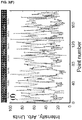
- FIG. 1 is an XRD pattern of Mo 2 Ga 2 C thin film sample.
- the other 9 peaks come from the thin film and represent a series of interplanar spacing d with a least common multiple of ⁇ 9.04 ⁇ .
- FIG. 2 illustrates (A) Selected area electron diffraction of Mo 2 Ga 2 C thin films in [11 20 ] and, (B) [1010] zone axes, (C) EDS spectrum; (D) high-angle annular dark field (HAADF) images in the (D) [11 20 ] and, (E) [1010] zone axes.
- Insets are corresponding atomic structure models of indicating corresponding positions of Ga and Mo atoms in the stacking sequence
- FIG. 3 illustrates (A) HAADF image and corresponding (B), Mo, (C) Ga, and, (D) Mo and Ga maps, (E) HAADF image superimposed with Mo and Ga maps, (F) line scan along [0001] direction a Mo 2 Ga 2 C film (Ga, square points and Mo, circle points).
- FIG. 4 illustrates are powder XRD patterns indexed to Mo 2 Ga 2 C showing observed pattern (black crosses), Rietveld generated pattern (red line) and difference between the two (blue line).
- the ticks below the pattern represent the peak positions of Mo 2 Ga 2 C phase, Mo 2 C phase, and graphite phase, respectively.
- the ⁇ 2 value was 3.78.
- Inset shows schematic of unit cell.
- FIG. 5 is a scanning electron microscope micrograph of Mo 2 Ga 2 C powders showing typical MAX phase platelet morphology
- FIG. 6 is an XRD pattern of Mo 2 Ga 2 C bulk sample, the triangle markers represent peaks for free gallium.
- Mo 2 Ga 2 C is a particular embodiment within this class
- transitional terms “comprising,” “consisting essentially of” and “consisting” are intended to connote their generally in accepted meanings in the patent vernacular; that is, (i) “comprising,” which is synonymous with “including,” “containing,” or “characterized by,” is inclusive or open-ended and does not exclude additional, unrecited elements or method steps; (ii) “consisting of” excludes any element, step, or ingredient not specified in the claim; and (iii) “consisting essentially of” limits the scope of a claim to the specified materials or steps “and those that do not materially affect the basic and novel characteristic(s)” of the claimed invention.
- the basic and novel characteristic(s) is the novel structures described herein.
- the term “consisting essentially of molybenum, gallium, and carbon” refers to a composition containing at least these elements, but the presence of any additional elements is insufficient to compromise the crystalline 2-2-1 structure of the Mo 2 Ga 2 C MAX phase composition.
- Various embodiments of this invention provide for crystalline solids, each crystalline solid having an empirical formula of M 2 A 2 X.
- M is at least one Group IIIB, IVB, VB, or VIB metal, preferably Cr, Hf, Sc, Ti, Mo, Nb, Ta, V, Zr, or a combination thereof (more preferably Mo);
- A is Al, Ga, Ge, In, Pb, or Sn, or a combination thereof (preferably Ga);
- M refers to one or more members of the Groups IIIB, IVB, VB, or VIB or (aka) Groups 3-6 of the periodic table, either alone or in combination, said members at least including Sc, Y, Lu, Ti, Zr, Hf, V, Nb, Ta, Cr, Mo, and W.
- the terms “M” or “M atoms,” “M elements,” or “M metals” may also include Mn.
- the transition metal is one or more of Sc, Ti, Zr, Hf, V, Nb, Ta, Cr, and/or Mo. In even more preferred embodiments, the transition metal is Mo.
- these 2-2-1 crystalline solids also may include one or more of Cr 2 Ga 2 C, Cr 2 Ga 2 N, Mo 2 Ga 2 N, Nb 2 Ga 2 C, Nb 2 Ga 2 N, Ta 2 Ga 2 C, Ta 2 Ga 2 N, Ti 2 Ga 2 C, Ti 2 Ga 2 N, V 2 Ga 2 C, or V 2 Ga 2 N.
- these 2-2-1 crystalline solids may include one or more of Hf 2 In 2 C, Hf 2 In 2 N, Hf 2 Sn 2 C, Hf 2 Sn 2 N, Nb 2 In 2 C, Nb 2 In 2 N, Nb 2 Sn 2 C, Nb 2 Sn 2 N, Sc 2 In 2 C, Sc 2 In 2 N, Ti 2 In 2 C, Ti 2 In 2 N, Ti 2 Sn 2 C, Ti 2 Sn 2 N, Zr 2 In 2 C, Zr 2 In 2 N, Zr 2 Sn 2 C, or Zr 2 Sn 2 N.
- Atomic MAX Phase Radius, pm material? A-Element Aluminum 118 Yes Germanium 125 Yes Astatine 127 Yes Gallium 136 Yes Tin 145 Yes Lead 154 Yes Indium 156 Yes Thallium 156 Yes M-Element Chromium 166 Yes Vanadium 171 Yes Titanium 176 Yes Scandium 184 Yes Molybdenum 190 Yes Niobium 198 Yes Tantalum 200 Yes Zirconium 206 Yes Hafnium 208 Yes
- M n+1 AX n phase materials are themselves known to exist as laminated structures with anisotropic properties. These materials are layered hexagonal (space group P6 3 /mmc), with two formula units per unit cell. Such also appears to be the case with these new 2-2-1 MAX phase materials. Near close-packed M-layers are interleaved with pure A-group element layers, with the X-atoms filling the octahedral sites between the former. In the case of the 2-2-1 materials, the near close packed M-layers are interleaved with two A-group element layers.
- the 2-2-1 materials have structures characterized as comprising two layers of Ga, In, or Sn atoms stacked between the corresponding Cr 2 C, Cr 2 N, Hf 2 C, Hf 2 N, Mo 2 C, Mo 2 N, Nb 2 C, Nb 2 N, Sc 2 C, Sc 2 N, Ta 2 C, Ta 2 N, Ti 2 C, Ti 2 N, V 2 C, V 2 N, Zr 2 C, or Zr 2 N layers or mixed metal layers of TiZrC, TiZrN, TiHfC, TiHfN, ZrHfC, ZrHfN CrMoC, CrMoC, VTaC, VTaN, VNbC, VNbN, TaNbC, or TaNbN.
- This is demonstrated specifically for Mo 2 Ga 2 C, where two layers of Ga atoms are stacked between Mo 2 C layers, the structure exhibiting a simple hexagonal arrangement.
- 2-2-1 MAX-phase materials can also be characterized by their X-ray diffraction (XRD) spectra (see FIG. 1 and Table 1).
- XRD X-ray diffraction
- certain embodiments provide crystalline solids comprising or consisting essentially of molybdenum, gallium, and carbon exhibiting at least five of the following characteristic X-ray powder diffraction peaks (Cu K ⁇ radiation, expressed in degrees 2 ⁇ ) at approximately 9.8, 19.6, 29.6, 39.9, 50.4, 61.5, 73.2, 86.0, and 100.2.
- Additional embodiments include solids that further exhibit other additional peaks shown in FIG. 1 , preferably in order of decreasing intensities.
- crystalline solids comprising or consisting essentially of molybdenum, gallium, and carbon exhibiting at least five of the following characteristic X-ray powder diffraction peaks (Cu K ⁇ radiation, expressed in degrees 2 ⁇ ) at approximately 9.8, 34.1, 37.3, 42.5, 53.4, 61.0, and 75.4, and optionally other additional peaks shown in Table 1, preferably in order of decreasing intensities.
- M is at least one Group IIIB, IVB, VB, or VIB metal, preferably Cr, Hf, Sc, Ti, Mo, Nb, Ta, V, Zr, or a combination thereof.
- A is Al, Ga, Ge, In, Pb, or Sn, or a combination thereof and
- the crystalline solid of Embodiment 1 that is Cr 2 Ga 2 C, Cr 2 Ga 2 N, Mo 2 Ga 2 C, Nb 2 Ga 2 C, Ta 2 Ga 2 C, Ti 2 Ga 2 C, Ti 2 Ga 2 N, V 2 Ga 2 C, or V 2 Ga 2 N.
- Embodiment 1 that is Hf 2 In 2 C, Hf 2 In 2 N, Hf 2 Sn 2 C, Hf 2 Sn 2 N, Nb 2 In 2 C, Nb 2 In 2 N, Nb 2 Sn 2 C, Nb 2 Sn 2 N, Sc 2 In 2 C, Sc 2 In 2 N, Ti 2 In 2 C, Ti 2 In 2 N, Ti 2 Sn 2 C, Ti 2 Sn 2 N, Zr 2 In 2 C, Zr 2 In 2 N, Zr 2 Sn 2 C, or Zr 2 Sn 2 N.
- Embodiment 1 The crystalline solid of Embodiment 1, having a unit cell stoichiometry of Mo 2 Ga 2 C.
- Embodiment 5 The crystalline solid of Embodiment 5, in which two layers of Ga atoms are stacked between otherwise adjacent Mo 2 C layers.
- a crystalline solid comprising or consisting essentially of molybdenum, gallium, and carbon exhibiting at least five of the following characteristic X-ray powder diffraction peaks (Cu K ⁇ radiation, expressed in degrees 2 ⁇ ) at approximately 9.8, 19.6, 29.6, 39.9, 50.4, 61.5, 73.2, 86.0, and 100.2 and optionally other additional peaks shown in FIG. 1 , preferably in order of decreasing intensities.
- a crystalline solid comprising or consisting essentially of molybdenum, gallium, and carbon exhibiting at least five of the following characteristic X-ray powder diffraction peaks (Cu K ⁇ radiation, expressed in degrees 2 ⁇ ) at approximately 9.8, 34.1, 37.3, 42.5, 53.4, 61.0, and 75.4 and other additional peaks shown in Table 1, preferably in order of decreasing intensities.
- the starting materials used were commercial Mo (63 NS, Metco Inc., Anderson, S.C.), graphite (Grade 4827, Asbury Graphite Mills Inc., Asbury, N.J.) powders and Ga shots (99.99%) (Roto Metals Inc., San Leandro, Calif.).
- Mo and graphite powders were weighed in a 2:1 molar ratio and placed in a plastic bottle and mixed for 24 h using agate balls as the milling media. This mixture was then mixed with the Ga shot in an agate mortar.
- Powders of Mo 2 Ga 2 C were synthesized by a solid liquid reaction of Mo 2 C and Ga.
- a ⁇ 325 mesh Mo 2 C powder and Ga both from Alfa Aesar, Ward Hill, Mass., both of 99.5 wt % purity
- a quartz tube that was evacuated using a mechanical vacuum pump and sealed.
- the latter was placed in a horizontal tube furnace that was heated at a rate of 10° C. min ⁇ 1 to 850° C., and held at that temperature for 48 h. After furnace cooling, the lightly sintered material was crushed, using a mortar and pestle, and returned back to the quartz tube. The latter was evacuated and re-heated at a rate of 10° C.
- Mo 2 Ga 2 C powder was added to 20 mL of a premixed solution of 3 M of LiF (90+%, Ward Hill, Mass., Alfa Aesar) and 12 M HCl.
- the Mo 2 Ga 2 C containing mixture was placed on a magnetic stirrer hot plate in an oil bath held at 35° C. for various times. Afterwards, the mixture was washed through three cycles of 1 M of aqueous HCl, followed by three cycles of 1 M of aqueous LiCl (Alfa Aesar, 98+%), and finally cycles of DI water until the supernatant reached a pH of approximately 6.
- the washing was performed by adding 40 mL volume of the solution to the washed powders in a centrifuge tube, and the tube was hand-shaken for 1 min before centrifuging at 5000 rpm for 2 min. 20 mL of argon, Ar, deaerated DI water were then added to the washed powder, which was then hand shaken for 5 min., followed by centrifuging for 1 h at 5000 rpm. The supernatant was collected for further investigation. The settled powder was discarded.
- the product was characterized to be a MXene composition of Mo 2 CT x (i.e., a 2-D lattice having a unit cell composition of Mo 2 C where T x represents surface terminations of each crystal lattice layer, predominantly by O and OH) intercalated by lithium ions.
- Mo 2 CT x i.e., a 2-D lattice having a unit cell composition of Mo 2 C where T x represents surface terminations of each crystal lattice layer, predominantly by O and OH
- the Mo 2 Ga 2 C responded to this treatment with LiCl and HCl in much the same way as previously observed for extracting aluminum from MAX phase analogs.
- Powders of Mo 2 Ga 2 C were immersed, slowly, in a bottle containing 14 M aqueous HF (Fisher Scientific, Fair Lawn, N.J.) in a ratio of 1 g to 40 mL. Afterwards the bottle was placed in an oil bath over a stirred hot plate held at 55° C. for 160 h, while stirring using a Teflon coated magnet. The resulting suspension was washed with DI water through several cycles till a pH of ca. 6 was reached. In each cycle, the washing was performed by adding 40 mL of DI water to a centrifuge tube containing the sediment, and then the tube was hand-shaken for 1 min before centrifuging at 5000 rpm for 2 min. The settled powder was removed from the centrifuge tube and filtered through a nanoporous polypropylene membrane (3501 Coated PP, 0.064 micron pore size, Celgard) for further investigation.
- a nanoporous polypropylene membrane (3501 Coated PP, 0.064 micron
- Direct current magnetron sputtering was used to grow Mo—Ga—C thin films were synthesized.
- the films were co-deposited from three elemental targets, Mo (3-inch, 99.95% purity, SCOTECH Ltd.), Ga (2-inch, 99.99999% purity, 5N Plus UK Ltd.) and C (3-inch, 99.99% purity, SCOTECH Ltd.) with respective powers 40 W, 18 W and 200 W and at ⁇ 0.5 Pa Ar with a background pressure in the range of 10-7 Pa. Due to its low melting point ( ⁇ 30° C.), the Ga source was kept in a concave stainless steel crucible right below the substrate, in line with previously developed procedures. The Mo and C targets were tilted +35° and ⁇ 35° away from the horizontal position of the Ga target, co-focusing onto the rotating substrate.
- the thin films were grown on MgO (111) substrates (10 ⁇ 10 ⁇ 0.5 mm 3 , Latech Ltd.) that were ultrasonically cleaned sequentially in acetone, ethanol and isopropanol for 10 minutes at each stage. Before deposition, the substrate was heated to 560° C. at the base pressure, followed by a 10 minutes presputtering with the same powers for deposition. A shutter was inserted to blind the substrate from the target's line-of-sight when pre-sputtering, and was afterwards removed directly to start the deposition at the same substrate temperature set-point (560° C.).
- XRD patterns were obtained with a diffractometer (Rikagu Smartlab, Tokyo, Japan), with a step size of 0.02° in the 3°-120° 2 theta range with a step time of 7 s with a 10 ⁇ 10 mm 2 window slit. Scans were made with Cu-K ⁇ radiation (40 kV and 44 mA).
- the TEM specimens were prepared by mechanic polishing followed by ion thinning down to electron transparency.
- High resolution scanning electron microscopy (HRSTEM) and X-ray energy dispersive spectroscopy (EDX) were performed with a double Cs corrected FEI Titan3 60-300 operated at 300 kV, equipped with the Super-X EDX system.
- Selected area electron diffraction (SAED) characterization was carried out using a FEI Tecnai G2 TF20 UT instrument operated at 200 kV with a point resolution of 0.19 nm.
- Structural characterization of the thin films was performed through X-ray diffraction (XRD).
- the system utilized was a Panalytical Empyrean MRD with a Cu K ⁇ source.
- the measurements performed were symmetric ( ⁇ -2 ⁇ ) scans obtained by employing a hybrid mirror and a 0.27° parallel plate collimator in the incident and the diffracted beam side, respectively.
- the new phase compositions may be produced in two forms: thin film and bulk.
- the thin films were grown by direct current magnetron sputtering of elemental targets on MgO (111) substrates.
- Bulk Mo 2 Ga 2 C samples were synthesized by, first heating a 2:1 molar ratio of Mo:C powders in flowing Ar at 1000° C. for 12 h. The resulting, lightly sintered, Mo 2 C compact was crushed into a powder and mixed with Ga in 1:1 molar ratio. This mixture was then sealed under a mechanical vacuum in a 100 mm long quartz tube, and sintered at 850° C. for 24 h. XRD diffraction patterns of the resulting material showed the presence of significant amounts of unreacted Ga. To dissolve the latter, the powders were immersed in 37% HCl for 4 days.
- FIGS. 2(A) and (B) are SAED patterns from the new compound.
- the phase has a hexagonal structure with a and c lattice parameters of 3.05 ⁇ and 18.19 ⁇ , respectively.
- the possibility that those patterns originate from a 312 MAX structure can be excluded for the following reasons.
- the chemical composition analysis shown in FIG. 2(C) exhibits a different Mo/Ga ratio from that of Mo 3 GaC 2 phase.
- the structure is also not that of Ta 2 S 2 C and Nb 2 S 2 C phases, which have the same or at least similar “221” stoichiometries, since they belong to the space group R-3m.
- the stacking observed in HRSTEM (below) is inconsistent with either of these sulphides or a 312 MAX phase.
- FIG. 2(C) and FIG. 2(D) show HRSTEM images with the beam aligned along the [1120] and [1010] zone axes, respectively.
- the Z contrast images show a double-layer structural feature.
- the bright and dark spots should correspond to the Mo and Ga atoms, respectively.
- the corresponding EDX maps shown in FIG. 3 (A-F) confirm the Mo—Mo—Ga—Ga—Mo—Mo layering.
- the simplest description of the structure is the following: Start with a 211 MAX phase structure and simply insert one extra Ga layer on top of the existing Ga. Surprisingly, the two Ga layer lie exactly on top of each other (i.e. not close-packed), an unusual arrangement indeed. Indeed this stacking structure is further supported by the facile way in which Mo 2 Ga 2 C is convertible to Mo 2 C MXene with the removal of Ga. See Examples 1.3 and 1.4.
- the distance between adjacent Mo layers was estimated to be 2.27 ⁇ .
- the separation width between the Mo and Ga layers is shortest: 2.09 ⁇ .
- the same stacking position of the two adjacent Ga layers leads a large separation width.
- the separation width between the adjacent Ga layers is about 2.64 ⁇ .
- FIG. 4 shows a typical XRD pattern of the phase obtained after dissolving the unreacted Ga from the bulk sample.
- this new phase was imaged in a HRSTEM (see above) its structure was found to be unlike any other MAX phase known in that there were two Ga layers separating the Mo 2 C blocks. Making use of this insight, the XRD pattern was analyzed assuming the unit cell shown in inset of FIG. 4 .
Landscapes
- Chemical & Material Sciences (AREA)
- Organic Chemistry (AREA)
- Inorganic Chemistry (AREA)
- Crystallography & Structural Chemistry (AREA)
- Catalysts (AREA)
Abstract
Description
| Atomic | MAX Phase | |
| Radius, pm | material? | |
| A-Element | ||
| Aluminum | 118 | Yes |
| Germanium | 125 | Yes |
| Astatine | 127 | Yes |
| Gallium | 136 | Yes |
| Tin | 145 | Yes |
| Lead | 154 | Yes |
| Indium | 156 | Yes |
| Thallium | 156 | Yes |
| M-Element | ||
| Chromium | 166 | Yes |
| Vanadium | 171 | Yes |
| Titanium | 176 | Yes |
| Scandium | 184 | Yes |
| Molybdenum | 190 | Yes |
| Niobium | 198 | |
| Tantalum | ||
| 200 | Yes | |
| Zirconium | 206 | Yes |
| Hafnium | 208 | Yes |
| TABLE 1 |
| X-ray (Cu Kα) powder diffraction data for Mo2Ga2C. |
| Peak | |||||||
| Num- | I calcu- | I ob- | |||||
| ber | h | k | l | 2theta | lated | served | d-hkl |
| 1 | 0 | 0 | 2 | 9.778 | 539.2 | 595.1 | 9.038692 |
| 2 | 0 | 0 | 4 | 19.627 | 12.8 | 0 | 4.519346 |
| 3 | 0 | 0 | 6 | 29.626 | 9 | 5.4 | 3.012897 |
| 4 | 1 | 0 | 0 | 34.078 | 752.1 | 600 | 2.628786 |
| 5 | 1 | 0 | 1 | 34.448 | 111.7 | 87.2 | 2.601424 |
| 6 | 1 | 0 | 2 | 35.536 | 8.9 | 26.6 | 2.524197 |
| 7 | 1 | 0 | 3 | 37.289 | 1745.8 | 1612.5 | 2.409481 |
| 8 | 1 | 0 | 4 | 39.631 | 18.4 | 17.5 | 2.272329 |
| 9 | 0 | 0 | 8 | 39.862 | 661.3 | 741.6 | 2.259673 |
| 10 | 1 | 0 | 5 | 42.482 | 1469.5 | 1393.4 | 2.126176 |
| 11 | 1 | 0 | 6 | 45.77 | 14.5 | 85.8 | 1.980804 |
| 12 | 1 | 0 | 7 | 49.433 | 98.6 | 103.8 | 1.842244 |
| 13 | 0 | 0 | 10 | 50.442 | 7.3 | 6.8 | 1.807738 |
| 14 | 1 | 0 | 8 | 53.426 | 471.5 | 503.4 | 1.7136 |
| 15 | 1 | 0 | 9 | 57.715 | 2 | 0 | 1.596029 |
| 16 | 1 | 1 | 0 | 60.999 | 617.9 | 522.7 | 1.51773 |
| 17 | 0 | 0 | 12 | 61.505 | 13.5 | 12.9 | 1.506449 |
| 18 | 1 | 1 | 2 | 61.946 | 24.7 | 21.8 | 1.496776 |
| 19 | 1 | 0 | 10 | 62.281 | 11.7 | 9.9 | 1.489534 |
| 20 | 1 | 1 | 4 | 64.74 | 4 | 0 | 1.438764 |
| 21 | 1 | 0 | 11 | 67.115 | 230.1 | 182.8 | 1.393502 |
| 22 | 1 | 1 | 6 | 69.262 | 6.6 | 3.4 | 1.355463 |
| 23 | 2 | 0 | 0 | 71.754 | 84 | 53.4 | 1.314393 |
| 24 | 2 | 0 | 1 | 71.973 | 11.2 | 7.8 | 1.310932 |
| 25 | 1 | 0 | 12 | 72.22 | 7.6 | 7 | 1.307045 |
| 26 | 2 | 0 | 2 | 72.628 | 1.7 | 1.2 | 1.300712 |
| 27 | 0 | 0 | 14 | 73.247 | 1.7 | 1.6 | 1.291242 |
| 28 | 2 | 0 | 3 | 73.715 | 228.1 | 189.5 | 1.284197 |
| 29 | 2 | 0 | 4 | 75.227 | 2.2 | 2 | 1.262098 |
| 30 | 1 | 1 | 8 | 75.379 | 586.3 | 496.7 | 1.259917 |
| 31 | 2 | 0 | 5 | 77.155 | 244.3 | 208.9 | 1.235294 |
| 32 | 1 | 0 | 13 | 77.61 | 273.3 | 286.2 | 1.229188 |
| 33 | 2 | 0 | 6 | 79.492 | 3.1 | 6 | 1.204741 |
| 34 | 2 | 0 | 7 | 82.232 | 19.1 | 8.3 | 1.171398 |
| 35 | 1 | 1 | 10 | 83.011 | 12.4 | 10.1 | 1.162377 |
| 36 | 1 | 0 | 14 | 83.309 | 0.8 | 0.3 | 1.158976 |
| 37 | 2 | 0 | 8 | 85.372 | 119.4 | 93.3 | 1.136165 |
| 38 | 0 | 0 | 16 | 85.965 | 68.7 | 76.4 | 1.129836 |
| 39 | 2 | 0 | 9 | 88.914 | 0.3 | 0 | 1.099836 |
| 40 | 1 | 0 | 15 | 89.358 | 25.6 | 0 | 1.09552 |
| 41 | 1 | 1 | 12 | 92.183 | 26.6 | 30.9 | 1.069186 |
| 42 | 2 | 0 | 10 | 92.868 | 4.7 | 4.7 | 1.063088 |
| 43 | 1 | 0 | 16 | 95.818 | 75.3 | 80.9 | 1.038023 |
| 44 | 2 | 0 | 11 | 97.256 | 100.1 | 98.3 | 1.026468 |
| 45 | 0 | 0 | 18 | 100.17 | 3.6 | 4.2 | 1.004299 |
| 46 | 2 | 1 | 0 | 101.658 | 81.1 | 69.6 | 0.993588 |
| 47 | 2 | 1 | 1 | 101.871 | 7.7 | 6.7 | 0.99209 |
| 48 | 2 | 0 | 12 | 102.112 | 3.6 | 3.8 | 0.990402 |
| 49 | 2 | 1 | 2 | 102.509 | 2.6 | 3.9 | 0.987638 |
| 50 | 1 | 0 | 17 | 102.779 | 3.5 | 5.3 | 0.985778 |
| 51 | 1 | 1 | 14 | 103.116 | 8.1 | 12.3 | 0.983473 |
| 52 | 2 | 1 | 3 | 103.577 | 243.4 | 226.4 | 0.98035 |
| 53 | 2 | 1 | 4 | 105.081 | 2.4 | 4.4 | 0.970412 |
| 54 | 2 | 1 | 5 | 107.029 | 287.4 | 254.9 | 0.958068 |
| 55 | 2 | 0 | 13 | 107.494 | 161.1 | 148.3 | 0.955211 |
| 56 | 2 | 1 | 6 | 109.439 | 5.7 | 17.2 | 0.943602 |
| 57 | 1 | 0 | 18 | 110.383 | 3.3 | 6.7 | 0.938166 |
| 58 | 2 | 1 | 7 | 112.335 | 20.7 | 15.1 | 0.927322 |
| 59 | 2 | 0 | 14 | 113.494 | 1.1 | 0.2 | 0.921122 |
| 60 | 2 | 1 | 8 | 115.752 | 180.3 | 136.6 | 0.909545 |
| 61 | 1 | 1 | 16 | 116.411 | 317.9 | 288.6 | 0.906289 |
| 62 | 0 | 0 | 20 | 116.908 | 7.8 | 7.1 | 0.903869 |
| 63 | 1 | 0 | 19 | 118.859 | 74.3 | 57.1 | 0.894647 |
| 64 | 2 | 1 | 9 | 119.75 | 0.2 | 0.1 | 0.890583 |
| TABLE 2 |
| Atomic positions in Mo2Ga2C determined from Rietveld analysis |
| of XRD pattern shown in FIG. 1. The space group was P63/ |
| mmc. The a and c-lattice parameters were calculated |
| to be 3.03662(4) Å and 18.0855(3) Å, respectively. |
| Wykcoff | ||||
| Element | x | y | z | positions |
| Mo | ⅓ | ⅔ | 0.06434 (10) | 4f |
| Ga | ⅓ | ⅔ | 0.68238 (10) | |
| C | ||||
| 0 | 0 | 0 | 2a | |
- 1. M. W. Barsoum, MAX Phases: Properties of Machinable Carbides and Nitrides, Wiley VCH GmbH & Co., Weinheim, 2013.
- 2. P. Eklund, M. Beckers, U. Jansson, H. Hogberg and L. Hultman, Thin Solid Films, 2010, 518 1851-1878.
- 3. Z.-M. Sun, International Materials Reviews, 2011, 56, 143-166.
- 4. L. Toth, J. Less Comm. Met., 1967, 13 129˜131.
- 6. I. R. Shein and A. L. Ivanovskii, Physica C, 2010, 470, 533-537.
- 7. R. P. Ziebarth, J. K. Vassiliou and F. J. Disalvo, J. Less Comm. Met., 1989, 156, 207-211.
- 8. O. Beckmann, H. Boller and H. Nowotny, Monatsh. Chem., 1970, 101, 945 955.
- 9. H. Kudielka and H. Rohde, Z. Kristalogr., 1960, 114, 447.
- 10. H. Nowotny, Prog. Solid State Chem., 1970, 2, 27-70.
- 11. M. W. Barsoum, L. Farber, I. Levin, A. Procopio, T. El-Raghy and A. Berner, J. Amer. Cer. Soc., 1999, 82, 2545-2547.
- 12. A. Petruhins, A. S. Ingason, M. Dahlqvist, A. Mockute, M. Junaid, J. Birch, J. Lu, L. Hultman, P. O. Å. Persson and J. Rosen, Phys. Status Solidi RRL, vol. 7, no. 11, pp. 971-974, 2013.
Claims (12)
Priority Applications (1)
| Application Number | Priority Date | Filing Date | Title |
|---|---|---|---|
| US15/554,904 US10538431B2 (en) | 2015-03-04 | 2016-03-01 | Nanolaminated 2-2-1 MAX-phase compositions |
Applications Claiming Priority (3)
| Application Number | Priority Date | Filing Date | Title |
|---|---|---|---|
| US201562127907P | 2015-03-04 | 2015-03-04 | |
| PCT/US2016/020216 WO2016140948A1 (en) | 2015-03-04 | 2016-03-01 | Nanolaminated 2-2-1 max-phase compositions |
| US15/554,904 US10538431B2 (en) | 2015-03-04 | 2016-03-01 | Nanolaminated 2-2-1 MAX-phase compositions |
Publications (2)
| Publication Number | Publication Date |
|---|---|
| US20180044182A1 US20180044182A1 (en) | 2018-02-15 |
| US10538431B2 true US10538431B2 (en) | 2020-01-21 |
Family
ID=56848716
Family Applications (1)
| Application Number | Title | Priority Date | Filing Date |
|---|---|---|---|
| US15/554,904 Active - Reinstated US10538431B2 (en) | 2015-03-04 | 2016-03-01 | Nanolaminated 2-2-1 MAX-phase compositions |
Country Status (3)
| Country | Link |
|---|---|
| US (1) | US10538431B2 (en) |
| EP (1) | EP3265211B1 (en) |
| WO (1) | WO2016140948A1 (en) |
Families Citing this family (9)
| Publication number | Priority date | Publication date | Assignee | Title |
|---|---|---|---|---|
| EP3504288B1 (en) | 2016-08-25 | 2025-10-15 | Drexel University | Antennas comprising mx-ene films and composites |
| CN106986316B (en) * | 2017-05-05 | 2019-02-01 | 中国科学院过程工程研究所 | A kind of vanadium nitride material and its preparation method and application |
| US11925466B2 (en) | 2017-09-15 | 2024-03-12 | The Trustees Of The University Of Pennsylvania | Implantable devices using 2D metal carbides and nitrides (MXenes) |
| EP3778479B1 (en) * | 2018-07-10 | 2022-09-14 | Ningbo Institute of Materials Technology & Engineering, Chinese Academy of Sciences | Max phase material, preparation method therefor, and application thereof |
| WO2020252304A1 (en) | 2019-06-13 | 2020-12-17 | Drexel University | EDGE CAPPING OF 2D-MXene SHEETS WITH POLYANIONIC SALTS TO MIGITATE OXIDATION IN AQUEOUS COLLOIDAL SUSPENSIONS |
| CN111229272A (en) * | 2020-01-19 | 2020-06-05 | 华东师范大学 | Ternary layered carbide Mo2Ga2C composite flower-like MoS2 nanoparticle composite material and its preparation method and application |
| CN113178556B (en) * | 2021-04-23 | 2022-07-15 | 中国科学技术大学 | Mo2C@MoS2Heterojunction and preparation method and application thereof |
| CN113611469A (en) * | 2021-08-19 | 2021-11-05 | 中国科学技术大学 | A Ga-based MAX phase magnetic material and its preparation method and application |
| CN115483373B (en) * | 2022-08-23 | 2025-01-21 | 重庆长安新能源汽车科技有限公司 | A silicon composite material and its preparation method and application |
Citations (33)
| Publication number | Priority date | Publication date | Assignee | Title |
|---|---|---|---|---|
| US4801368A (en) | 1984-11-08 | 1989-01-31 | Tokuyama Soda Kabushiki Kaisha | Ni/Sn cathode having reduced hydrogen overvoltage |
| JPH0878018A (en) | 1994-08-31 | 1996-03-22 | Sanyo Electric Co Ltd | Lithium secondary battery |
| JPH10112316A (en) | 1996-10-08 | 1998-04-28 | Matsushita Electric Ind Co Ltd | Non-aqueous electrolyte secondary battery |
| EP0948067A1 (en) | 1998-04-03 | 1999-10-06 | Matsushita Electric Industrial Co., Ltd. | Non-aqueous electrolyte secondary battery |
| US6180049B1 (en) | 1999-06-28 | 2001-01-30 | Nanotek Instruments, Inc. | Layer manufacturing using focused chemical vapor deposition |
| US20020068488A1 (en) | 2000-08-28 | 2002-06-06 | Boston Microsystems, Inc. | Stable electrical contact for silicon carbide devices |
| WO2002081372A2 (en) | 2001-04-06 | 2002-10-17 | Carnegie Mellon University | A process for the preparation of nanostructured materials |
| WO2002096799A2 (en) | 2001-05-25 | 2002-12-05 | Max-Planck-Gesellschaft Zur | Silicon subnitride method for production and use of said subnitride |
| US6555268B1 (en) | 1998-06-09 | 2003-04-29 | Matsushita Electric Industrial Co., Ltd. | Negative electrode for secondary cell, negative plate for secondary cell, and secondary cell comprising the same |
| US20030148184A1 (en) | 2001-04-09 | 2003-08-07 | Atsuo Omaru | Negative electrode for non-aqueous electrolyte secondary cell, and non-aqueous electrolyte secondary cell using the negative electrode |
| US20030224168A1 (en) | 2002-05-30 | 2003-12-04 | The Regents Of The University Of California | Chemical manufacture of nanostructured materials |
| US20040048157A1 (en) | 2002-09-11 | 2004-03-11 | Neudecker Bernd J. | Lithium vanadium oxide thin-film battery |
| US20040229028A1 (en) | 2002-12-27 | 2004-11-18 | Fuji Photo Film Co., Ltd. | Method for producing light-transmitting electromagnetic wave-shielding film, light-transmitting electromagnetic wave-shielding film and plasma display panel using the shielding film |
| WO2005007566A2 (en) | 2003-07-03 | 2005-01-27 | Drexel University | Nanoporous carbide derived carbon with tunable pore size |
| JP2005158725A (en) | 2003-11-06 | 2005-06-16 | Showa Denko Kk | Graphite particle for negative pole material, manufacturing method for the same, and battery using the same |
| WO2006112869A2 (en) | 2004-07-19 | 2006-10-26 | Baylor College Of Medicine | Modulation of cytokine signaling regulators and applications for immunotherapy |
| US20070065725A1 (en) | 2003-10-17 | 2007-03-22 | Takao Inoue | Nonaqueous electrolyte battery |
| US20070066503A1 (en) | 2005-08-19 | 2007-03-22 | Mores Basaly | Methods and compositions for acid treatment of a metal surface |
| WO2007093011A1 (en) | 2006-02-17 | 2007-08-23 | Newcastle Innovation Limited | Crystalline ternary ceramic precursors |
| JP2007214137A (en) | 2007-03-12 | 2007-08-23 | Mitsubishi Chemicals Corp | Anode active material for non-aqueous carbon-coated lithium secondary battery |
| WO2007121931A2 (en) | 2006-04-24 | 2007-11-01 | Treibacher Industrie Ag | Hard metal body formed from a mixture containing a tungsten-cobalt-carbon |
| US7446190B2 (en) | 2002-05-28 | 2008-11-04 | Sloan-Kettering Institute For Cancer Research | Nucleic acids encoding chimeric T cell receptors |
| WO2009063031A2 (en) | 2007-11-16 | 2009-05-22 | Akzo Nobel N.V. | Electrode |
| WO2009091826A2 (en) | 2008-01-14 | 2009-07-23 | The Board Of Regents Of The University Of Texas System | Compositions and methods related to a human cd19-specific chimeric antigen receptor (h-car) |
| WO2010128492A1 (en) | 2009-05-08 | 2010-11-11 | Element Six (Production) (Pty) Ltd | Ultra-hard diamond composites |
| US20100322909A1 (en) | 2009-06-17 | 2010-12-23 | The University Of Pittsburgh - Of The Commonwealth System Of Higher Education | Th1-associated micrornas and their use for tumor immunotherapy |
| US20110017585A1 (en) | 2009-07-27 | 2011-01-27 | Aruna Zhamu | Mass production of pristine nano graphene materials |
| US20110104464A1 (en) | 2008-06-06 | 2011-05-05 | Pyzik Aleksander J | Metal-infiltrated titanium-silicon-carbide and titanium-aluminum-carbide bodies |
| US20120247800A1 (en) | 2009-04-24 | 2012-10-04 | Applied Nanostructured Solutions, Llc | Cns-shielded wires |
| US20130092428A1 (en) | 2010-04-15 | 2013-04-18 | Toshiyuki Kawaguchi | Printed wiring board and method of manufacture thereof |
| WO2014088995A1 (en) | 2012-12-04 | 2014-06-12 | Drexel University | Compositions comprising free-standing two-dimensional nanocrystal |
| US20140162130A1 (en) | 2011-06-21 | 2014-06-12 | Drexel University | Compositions comprising free-standing two-dimensional nanocrystals |
| US20150306570A1 (en) | 2014-04-29 | 2015-10-29 | Ut-Battelle, Llc | Metal-carbon composites and methods for their production |
Family Cites Families (2)
| Publication number | Priority date | Publication date | Assignee | Title |
|---|---|---|---|---|
| CH630745A5 (en) * | 1981-01-15 | 1982-06-30 | Jean Felix Orsini | Solar cell and process for manufacturing it |
| CN106986316B (en) * | 2017-05-05 | 2019-02-01 | 中国科学院过程工程研究所 | A kind of vanadium nitride material and its preparation method and application |
-
2016
- 2016-03-01 US US15/554,904 patent/US10538431B2/en active Active - Reinstated
- 2016-03-01 EP EP16759342.5A patent/EP3265211B1/en active Active
- 2016-03-01 WO PCT/US2016/020216 patent/WO2016140948A1/en not_active Ceased
Patent Citations (37)
| Publication number | Priority date | Publication date | Assignee | Title |
|---|---|---|---|---|
| US4801368A (en) | 1984-11-08 | 1989-01-31 | Tokuyama Soda Kabushiki Kaisha | Ni/Sn cathode having reduced hydrogen overvoltage |
| JPH0878018A (en) | 1994-08-31 | 1996-03-22 | Sanyo Electric Co Ltd | Lithium secondary battery |
| JPH10112316A (en) | 1996-10-08 | 1998-04-28 | Matsushita Electric Ind Co Ltd | Non-aqueous electrolyte secondary battery |
| EP0948067A1 (en) | 1998-04-03 | 1999-10-06 | Matsushita Electric Industrial Co., Ltd. | Non-aqueous electrolyte secondary battery |
| US6555268B1 (en) | 1998-06-09 | 2003-04-29 | Matsushita Electric Industrial Co., Ltd. | Negative electrode for secondary cell, negative plate for secondary cell, and secondary cell comprising the same |
| US6180049B1 (en) | 1999-06-28 | 2001-01-30 | Nanotek Instruments, Inc. | Layer manufacturing using focused chemical vapor deposition |
| US20020068488A1 (en) | 2000-08-28 | 2002-06-06 | Boston Microsystems, Inc. | Stable electrical contact for silicon carbide devices |
| WO2002081372A2 (en) | 2001-04-06 | 2002-10-17 | Carnegie Mellon University | A process for the preparation of nanostructured materials |
| US20030148184A1 (en) | 2001-04-09 | 2003-08-07 | Atsuo Omaru | Negative electrode for non-aqueous electrolyte secondary cell, and non-aqueous electrolyte secondary cell using the negative electrode |
| EP1381099A1 (en) | 2001-04-09 | 2004-01-14 | Sony Corporation | Negative electrode for non-aqueous electrolyte secondary cell and non-aqueous electrolyte secondary cell using the negative electrode |
| WO2002096799A2 (en) | 2001-05-25 | 2002-12-05 | Max-Planck-Gesellschaft Zur | Silicon subnitride method for production and use of said subnitride |
| US7446190B2 (en) | 2002-05-28 | 2008-11-04 | Sloan-Kettering Institute For Cancer Research | Nucleic acids encoding chimeric T cell receptors |
| US20030224168A1 (en) | 2002-05-30 | 2003-12-04 | The Regents Of The University Of California | Chemical manufacture of nanostructured materials |
| US20040048157A1 (en) | 2002-09-11 | 2004-03-11 | Neudecker Bernd J. | Lithium vanadium oxide thin-film battery |
| US20040229028A1 (en) | 2002-12-27 | 2004-11-18 | Fuji Photo Film Co., Ltd. | Method for producing light-transmitting electromagnetic wave-shielding film, light-transmitting electromagnetic wave-shielding film and plasma display panel using the shielding film |
| WO2005007566A2 (en) | 2003-07-03 | 2005-01-27 | Drexel University | Nanoporous carbide derived carbon with tunable pore size |
| US20070065725A1 (en) | 2003-10-17 | 2007-03-22 | Takao Inoue | Nonaqueous electrolyte battery |
| JP2005158725A (en) | 2003-11-06 | 2005-06-16 | Showa Denko Kk | Graphite particle for negative pole material, manufacturing method for the same, and battery using the same |
| WO2006112869A2 (en) | 2004-07-19 | 2006-10-26 | Baylor College Of Medicine | Modulation of cytokine signaling regulators and applications for immunotherapy |
| US20070066503A1 (en) | 2005-08-19 | 2007-03-22 | Mores Basaly | Methods and compositions for acid treatment of a metal surface |
| WO2007093011A1 (en) | 2006-02-17 | 2007-08-23 | Newcastle Innovation Limited | Crystalline ternary ceramic precursors |
| US20090017332A1 (en) | 2006-02-17 | 2009-01-15 | Newcastle Innovation Limited | Crystalline ternary ceramic precursors |
| WO2007121931A2 (en) | 2006-04-24 | 2007-11-01 | Treibacher Industrie Ag | Hard metal body formed from a mixture containing a tungsten-cobalt-carbon |
| JP2007214137A (en) | 2007-03-12 | 2007-08-23 | Mitsubishi Chemicals Corp | Anode active material for non-aqueous carbon-coated lithium secondary battery |
| WO2009063031A2 (en) | 2007-11-16 | 2009-05-22 | Akzo Nobel N.V. | Electrode |
| US20100236937A1 (en) | 2007-11-16 | 2010-09-23 | Akzo Nobel N.V. | Electrode |
| WO2009091826A2 (en) | 2008-01-14 | 2009-07-23 | The Board Of Regents Of The University Of Texas System | Compositions and methods related to a human cd19-specific chimeric antigen receptor (h-car) |
| US20110104464A1 (en) | 2008-06-06 | 2011-05-05 | Pyzik Aleksander J | Metal-infiltrated titanium-silicon-carbide and titanium-aluminum-carbide bodies |
| US20120247800A1 (en) | 2009-04-24 | 2012-10-04 | Applied Nanostructured Solutions, Llc | Cns-shielded wires |
| WO2010128492A1 (en) | 2009-05-08 | 2010-11-11 | Element Six (Production) (Pty) Ltd | Ultra-hard diamond composites |
| US20100322909A1 (en) | 2009-06-17 | 2010-12-23 | The University Of Pittsburgh - Of The Commonwealth System Of Higher Education | Th1-associated micrornas and their use for tumor immunotherapy |
| US20110017585A1 (en) | 2009-07-27 | 2011-01-27 | Aruna Zhamu | Mass production of pristine nano graphene materials |
| US20130092428A1 (en) | 2010-04-15 | 2013-04-18 | Toshiyuki Kawaguchi | Printed wiring board and method of manufacture thereof |
| US20140162130A1 (en) | 2011-06-21 | 2014-06-12 | Drexel University | Compositions comprising free-standing two-dimensional nanocrystals |
| US20150210044A1 (en) | 2011-06-21 | 2015-07-30 | Drexel University | Compositions comprising free-standing two-dimensional nanocrystals |
| WO2014088995A1 (en) | 2012-12-04 | 2014-06-12 | Drexel University | Compositions comprising free-standing two-dimensional nanocrystal |
| US20150306570A1 (en) | 2014-04-29 | 2015-10-29 | Ut-Battelle, Llc | Metal-carbon composites and methods for their production |
Non-Patent Citations (57)
| Title |
|---|
| Barsoum et al, "Room-Temperature Deintercalation and Self-Extrusion of Ga from Cr2GaN", Science, May 7, 1999, 284(5416), 937-939. |
| Barsoum et al, "The Topotactic Transformation of Ti3SiC2 into a Partially Ordered Cubic Ti(C0.67Si0.06) Phase by the Diffusion of Si into Molten Cryolite", Journal of the Electrochemical Society, 1999, 146(10), 3919-3923. |
| Barsoum, "Physical Properties of the MAX phases", Encyclopedia of Materials: Science and Technology, 2006, 11 pages. |
| Barsoum, et al., "Synthesis and Characterization of a Remarkable Ceramic: Ti3SiC2," J Amer. Chem. Soc., 1996 79(7), 1953-1956. |
| Barsoum, M. and El-Raghy, T., "The MAX Phases: Unique New Carbide and Nitride Materials", American Scientist, Jul.-Aug. 2001, 89:334-343. |
| Barsoum, M., "The MN+1AXN phases: New Class of Solids", Progress in Solid State Chemistry, Jan. 1, 2000, 28(1-4), 201-281. |
| Chang et al., "Synthesis of a new graphene-like transition metal carbide by de-intercalating Ti3AlC2", Mater. Lett., Oct. 2013, 109, 295-298. |
| Chen et al, "Microstructure and Phase Transformation of Ti 3 Ac 2 (A= Al, Si) in Hydrofluoric Acid Solution", Crystal Research and Technology, Oct. 27, 2014, 49(10), 813-819. |
| Chen et al., "In-situ synthesis of Ti3AlC2/TiC-A120O3 composite from TiO2-Al-C system", Journal of Materials Science & Technology, 2006, 22, 455-458. |
| Chen et al., "In-situ synthesis of Ti3AlC2/TiC-A120O3 composite from TiO2—Al—C system", Journal of Materials Science & Technology, 2006, 22, 455-458. |
| Coleman et al, "Two-Dimensional Nanosheets Produced by Liquid Exfoliation of Layered Materials", Science, Feb. 4, 2011, 331, 568-571. |
| Eis, PS et al, Accumulation of miR-155 and BIC RNA in Human B Cell Lymphomas. Proceedings of the National Academy of Sciences of the United States of America, Mar. 8, 2005, 102(10), 3627-3632, Abstract. |
| Eklund et al, "The Mn+1AXn Phases: Materials Science and Thin-Film Processing", Thin Solid Films, 2010, 518, 1851-1878. |
| Ettmayer et al., "Crystal structure of Cr3(C,N)2 and CrVC2", Monatshefte fur Chemie and Verwandte Teile Anderer Wissenschaften, Jul. 1966, vol. 97, Issue 4, 1258-1262. |
| European Patent Application No. 12803351.1: Supplementary European Search Report dated Jan. 30, 2015, 14 pages. |
| Finkel et al., "Magnetotransport properties of the ternary carbide Ti3SiC2: Hall effect, magnetoresistance, and magnetic susceptibility", Physical Review B, Jan. 15, 2002, vol. 65, Issue 3, 4 pages. |
| Ghidiu et al., "Conductive two-dimensional titanium carbide 'clay' with high volumetric capacitance", Nature, Dec. 2014, 516, 78-81. |
| Ghidiu et al., "Conductive two-dimensional titanium carbide ‘clay’ with high volumetric capacitance", Nature, Dec. 2014, 516, 78-81. |
| Halim et al., "Transparent Conductive Two-Dimensional Titanium Carbide Epitaxial Thin Films", Chem. Mater., 2014, vol. 26, No. 7, 2374-2381, Abstract; p. 2376, Scheme 1, p. 2379, col. 1, para. 2; p. 2379, col. 2, para. 2. |
| Henadaoui et al., "Ti-Al-C MAX Phases by Aluminothermic Reduction process", International Journal of Self-Propagating High-Temperature Synthesis, 2008, 17, 125-128. |
| Henadaoui et al., "Ti—Al—C MAX Phases by Aluminothermic Reduction process", International Journal of Self-Propagating High-Temperature Synthesis, 2008, 17, 125-128. |
| Hu et al. "Two-dimensional Sc2C: A reversible and high-capacity hydrogen storage material predicted by first principles calculations", International Journal of Hydrogen Energy, Jul. 2014, 39, 20, 10606-10612. |
| Hu et al., "MXene: A New Family of Promising Hydrogen Storage Medium", J. Phys. Chem A, 2013, 117, 14523-14260. |
| Hu et al.; Mo2Ga2C: a new ternary nanolanninated carbide; Chem. Commun., 51, 6560-6563; Mar. 2015. * |
| Hu, C., "Low Temperature Thermal Expansion, High Temperature Electrical Conductivity, and Mechanical Properties of Nb4AlC3 Ceramic Synthesized by Spark Plasma Sintering", Journal of Alloys and Compounds, Nov. 13, 2009, 487(1-2), 675-681. |
| International Patent Application No. PCT/US13/072733: The International Search Report and the Written Opinion dated Mar. 28, 2014, pp. 1-12. |
| International Patent Application No. PCT/US13/64503: The International Search Report and the Written Opinion dated Jan. 24, 2014, pp. 1-13. |
| Jin et al., "Synthesis of VC-Cr3C2 Nanocomposite Powders by Carbothermal Reduction", Nanoscience and Nanotechnology Letters, Oct. 2012, vol. 4, No. 10, 1028-1030, Abstract, 1 page. |
| Jin et al., "Synthesis of VC—Cr3C2 Nanocomposite Powders by Carbothermal Reduction", Nanoscience and Nanotechnology Letters, Oct. 2012, vol. 4, No. 10, 1028-1030, Abstract, 1 page. |
| Korzhavyi et al, "Ab Initio Study of Phase Equilibria in TiCx", Physical Review Letters, Dec. 18, 2001, 88(1), 1-4. |
| Kulkarni et al, Thermal Expansion and Stability of Ti2SC in Air and Inert Atmospheres, Journal of Alloys and Compounds, 2009, 469, 395-400. |
| Mogilevsky et al, "The Structure of Multilayered Titania Nanotubes Based on Delaminated Anatase", Chemical Physics Letters, 2008, 460, 517-520. |
| Myhra, et al., "Crystal-Chemistry of the Ti3AlC2 and Ti4AlN Layered Carbide/Nitride Phases-Characterization by XPS", Journal of Physics and Chemistry of Solids, Apr. 2001, vol. 62(4), 811-817. |
| Myhra, et al., "Crystal-Chemistry of the Ti3AlC2 and Ti4AlN Layered Carbide/Nitride Phases—Characterization by XPS", Journal of Physics and Chemistry of Solids, Apr. 2001, vol. 62(4), 811-817. |
| Nadeau, "Clay Particle Engineering: a Potential New Technology with Diverse Applications", Applied Clay Science, 1987, 2, 83-93. |
| Naguib et al, "Mxene: A Promising Transition Metal Carbide Anode for Lithium-ion Batteries", Electrochemistry Communications, 2012, 16, 61-64. |
| Naguib et al, "New Two-dimensional Niobium and Vanadium Carbides as Promising Materials for Li-Ion Batteries", American Chemical Society, Oct. 2013, 135(43), 15966-15969. |
| Naguib et al, "Two-Dimensional Nanocrystals Produced by Exfoliation of Ti3AlC2", Advanced Materials, 2011, 23, 4248-4253. |
| Naguib et al, "Two-Dimensional Transition Metal Carbides", American Chemical Society, Feb. 2012, 6(2), 1322-1331. |
| Naguib et al, Synthesis of a New Nanocrystalline Titanium Aluminum Fluoride Phase by Reaction of Ti2aic With Hydrofluoric Acid, RSC Adv. 1: 1493-1499, 2011. [retrieved on Mar. 7, 2014]. Retrieved from the internet: <URL: http://pubs.rsc.org .ezproxy.neu.ed u/en/Content/Articlelanding/2011/RA/c1raO0390a#/div, Abstract. |
| Naguib et al., "Mxenes: A new family of two-dimensional materials", Advanced Materials, 2014, 26, 992-1005. |
| Nan et al., "Percolation phenomena in niobium-doped TiC1-x", Materials Science and Engineering B-Solid State Materials for Advanced Technology, Feb. 1991, vol. 7, Issue 4, 283-286. |
| Peng et al., "Unique lead adsorption behavior of activated hydroxyl group in two-dimensional titanium carbide", Journal of the American Chemical Society, 2014, 136, 4113-4116. |
| Rao et al, "A Study of the Synthetic Methods and Properties of Graphenes", Science and Technology of Advanced Materials, 11, Oct. 27, 2010, 1-15. |
| Rudy, "Crystal structure of Ta2VC2", Journal of the Less-Common Motale, Jan. 1970, vol. 20, Issue 1, 49-55. |
| Savoskin et al, "Carbon Nanoscrolls Produced From Acceptor-Type Graphite Intercalation Compounds", 2007, Carbon, 45, 2797-2800. |
| Schmidt, et al., "XPS Studies of Amino Acids Absorbed on Titanium Dioxide Surfaces", Fresenius Journal of Analytical Chemistry, May 1991, 341, 412-415. |
| Spanier et al, "Vibrational Behavior of the Mn+1AXn phases from First-Order Raman Scattering ,,M=Ti ,V,Cr, A=Si, X=C,N)", Physical Review B, Jan. 2005, 71, 1-4. |
| Srinivasan, "Batteries for Advanced Transportation Technologies (BATT) Program. The fourth quarter 2014 FY report", Berkeley National Laboratory Document, Nov. 19, 2014, http://bmr.lbl.gov/wp-content/uploads/sites/3battfiles/reports/BATT_2014_4th_Quarterly_Report.pdf, 74 pages. |
| Stankovich et al, "Graphene-based Composite Materials", Nature, Jul. 2006, 442, 282-286. |
| Su et al., "High-Quality Thin Graphene Films from Fast Electrochemical Exfoliation", ACS Nano, 2011, 5(3), 2332-2339. |
| Tang et al., "Are MXenes Promising Anode Materials for Li Ion Batteries? Computational Studies on Electronic Properties and Li Storage Capability of Ti3C2 and Ti3C2X2 (X=F, OH) Monolayer", Journal of the American Chemical Society, 2012, 134, 16909-16916. |
| Tran et al, "Lithium Intercalation in Porous Carbon Electrodes", Material Research Society 1995 Spring Meeting, San Francisco, CA, Apr. 17-21, 1995, 12 Pages. |
| Travaglini et al, "The Corrosion Behavior of Ti3SiC2 in Common Acids and Dilute NaOH", Corrosion Science, Jun. 1, 2003, 45(6), 1313-1327. |
| Tzenov et al, "Synthesis and Characterization of Ti3AlC2", Journal of the American Ceramic Society, Jan. 1, 2000, 83(4), 825-832. |
| Viculis et al, "A Chemical Route to Carbon Nanoscrolls", Science, Feb. 28, 2003, 299, p. 1361. |
| Viculis, et al., "Intercalation and Exfoliation Routes to Graphite Nanoplatelets", Journal of Materials Chemistry, 2005, vol. 15, 974-978. |
Also Published As
| Publication number | Publication date |
|---|---|
| WO2016140948A1 (en) | 2016-09-09 |
| US20180044182A1 (en) | 2018-02-15 |
| EP3265211A4 (en) | 2018-08-01 |
| EP3265211B1 (en) | 2019-12-04 |
| EP3265211A1 (en) | 2018-01-10 |
Similar Documents
| Publication | Publication Date | Title |
|---|---|---|
| US10538431B2 (en) | Nanolaminated 2-2-1 MAX-phase compositions | |
| Hu et al. | Mo 2 Ga 2 C: a new ternary nanolaminated carbide | |
| Zhang et al. | Crystal structure of Cr4AlB4: A new MAB phase compound discovered in Cr-Al-B system | |
| US11411218B2 (en) | Two-dimensional, ordered, double transition metals carbides having a nominal unit cell composition M′2M″NXN+1 | |
| KR102737524B1 (en) | Formation of LimMOxFy Shell on Cathode Ceramic Particles for Li-ion Battery via Onium Metal Oxide Fluoride Precursor | |
| Högberg et al. | Epitaxial Ti2GeC, Ti3GeC2, and Ti4GeC3 MAX-phase thin films grown by magnetron sputtering | |
| Meshkian et al. | Theoretical stability and materials synthesis of a chemically ordered MAX phase, Mo2ScAlC2, and its two-dimensional derivate Mo2ScC2 MXene | |
| Lalère et al. | Improving the energy density of Na 3 V 2 (PO 4) 3-based positive electrodes through V/Al substitution | |
| JP7034471B2 (en) | Potassium compound and positive electrode active material for potassium ion secondary battery containing it | |
| WO2017044262A1 (en) | Improved routes to mx-ene carbides | |
| Liu et al. | MOF membrane synthesis in the confined space of a vertically aligned LDH network | |
| KR20180090186A (en) | Method for producing garnet type oxide solid electrolyte | |
| Chen et al. | Two‐dimensional MXenes derived from medium/high‐entropy MAX phases M2GaC (M= Ti/V/Nb/Ta/Mo) and their electrochemical performance | |
| Naguib et al. | Synthesis of a new nanocrystalline titanium aluminum fluoride phase by reaction of Ti 2 AlC with hydrofluoric acid | |
| WO2021072150A1 (en) | Mxene compositions featuring five atomic layers | |
| Kim et al. | Additive-free synthesis of Li 4 Ti 5 O 12 nanowire arrays on freestanding ultrathin graphite as a hybrid anode for flexible lithium ion batteries | |
| Rehnlund et al. | Electrochemical fabrication and characterization of Cu/Cu 2 O multi-layered micro and nanorods in Li-ion batteries | |
| Ta et al. | Hydrothermal synthesis of Na4Mn9O18 nanowires for sodium ion batteries | |
| Glöcklhofer et al. | Dicyano-and tetracyanopentacene: foundation of an intriguing new class of easy-to-synthesize organic semiconductors | |
| Higashi et al. | Crystal structure of MoB2 | |
| Yamada et al. | BDH‐TTP as a Structural Isomer of BEDT‐TTF, and Its Two‐Dimensional Hexafluorophosphate Salt | |
| Kim et al. | Oxygen-tuned aluminum-based halide solid electrolytes enabling low-voltage anode compatibility in all-solid-state batteries | |
| Wang et al. | Solid state synthesis of a new ternary nitride MgMoN 2 nanosheets and micromeshes | |
| Ivanova et al. | Theoretical and experimental comparative study of the stability and phase transformations of sesquichalcogenides M 2 Q 3 (M= Nb, Mo; Q= S, Se) | |
| EP3325412A1 (en) | Tin-containing compounds |
Legal Events
| Date | Code | Title | Description |
|---|---|---|---|
| AS | Assignment |
Owner name: DREXEL UNIVERSITY, PENNSYLVANIA Free format text: ASSIGNMENT OF ASSIGNORS INTEREST;ASSIGNORS:BARSOUM, MICHEL W.;HU, CHUNFENG;SIGNING DATES FROM 20150327 TO 20150416;REEL/FRAME:043463/0968 |
|
| FEPP | Fee payment procedure |
Free format text: ENTITY STATUS SET TO UNDISCOUNTED (ORIGINAL EVENT CODE: BIG.); ENTITY STATUS OF PATENT OWNER: SMALL ENTITY |
|
| FEPP | Fee payment procedure |
Free format text: ENTITY STATUS SET TO SMALL (ORIGINAL EVENT CODE: SMAL); ENTITY STATUS OF PATENT OWNER: SMALL ENTITY |
|
| STPP | Information on status: patent application and granting procedure in general |
Free format text: RESPONSE TO NON-FINAL OFFICE ACTION ENTERED AND FORWARDED TO EXAMINER |
|
| STPP | Information on status: patent application and granting procedure in general |
Free format text: NON FINAL ACTION MAILED |
|
| STPP | Information on status: patent application and granting procedure in general |
Free format text: RESPONSE TO NON-FINAL OFFICE ACTION ENTERED AND FORWARDED TO EXAMINER |
|
| AS | Assignment |
Owner name: NATIONAL SCIENCE FOUNDATION, VIRGINIA Free format text: CONFIRMATORY LICENSE;ASSIGNOR:DREXEL UNIVERSITY;REEL/FRAME:050579/0985 Effective date: 20190822 |
|
| STPP | Information on status: patent application and granting procedure in general |
Free format text: AWAITING TC RESP., ISSUE FEE NOT PAID |
|
| STPP | Information on status: patent application and granting procedure in general |
Free format text: PUBLICATIONS -- ISSUE FEE PAYMENT VERIFIED |
|
| STCF | Information on status: patent grant |
Free format text: PATENTED CASE |
|
| FEPP | Fee payment procedure |
Free format text: MAINTENANCE FEE REMINDER MAILED (ORIGINAL EVENT CODE: REM.); ENTITY STATUS OF PATENT OWNER: SMALL ENTITY |
|
| LAPS | Lapse for failure to pay maintenance fees |
Free format text: PATENT EXPIRED FOR FAILURE TO PAY MAINTENANCE FEES (ORIGINAL EVENT CODE: EXP.); ENTITY STATUS OF PATENT OWNER: SMALL ENTITY |
|
| STCH | Information on status: patent discontinuation |
Free format text: PATENT EXPIRED DUE TO NONPAYMENT OF MAINTENANCE FEES UNDER 37 CFR 1.362 |
|
| FP | Lapsed due to failure to pay maintenance fee |
Effective date: 20240121 |
|
| PRDP | Patent reinstated due to the acceptance of a late maintenance fee |
Effective date: 20250513 |
|
| FEPP | Fee payment procedure |
Free format text: PETITION RELATED TO MAINTENANCE FEES FILED (ORIGINAL EVENT CODE: PMFP); ENTITY STATUS OF PATENT OWNER: SMALL ENTITY Free format text: PETITION RELATED TO MAINTENANCE FEES GRANTED (ORIGINAL EVENT CODE: PMFG); ENTITY STATUS OF PATENT OWNER: SMALL ENTITY Free format text: SURCHARGE, PETITION TO ACCEPT PYMT AFTER EXP, UNINTENTIONAL. (ORIGINAL EVENT CODE: M2558); ENTITY STATUS OF PATENT OWNER: SMALL ENTITY |
|
| MAFP | Maintenance fee payment |
Free format text: PAYMENT OF MAINTENANCE FEE, 4TH YR, SMALL ENTITY (ORIGINAL EVENT CODE: M2551); ENTITY STATUS OF PATENT OWNER: SMALL ENTITY Year of fee payment: 4 |
|
| STCF | Information on status: patent grant |
Free format text: PATENTED CASE |