US10520679B2 - Fiber alignment to photonics chip - Google Patents
Fiber alignment to photonics chip Download PDFInfo
- Publication number
- US10520679B2 US10520679B2 US16/000,011 US201816000011A US10520679B2 US 10520679 B2 US10520679 B2 US 10520679B2 US 201816000011 A US201816000011 A US 201816000011A US 10520679 B2 US10520679 B2 US 10520679B2
- Authority
- US
- United States
- Prior art keywords
- waveguide structure
- semiconductor substrate
- composite adhesive
- optical fiber
- bridge waveguide
- Prior art date
- Legal status (The legal status is an assumption and is not a legal conclusion. Google has not performed a legal analysis and makes no representation as to the accuracy of the status listed.)
- Active
Links
Images


Classifications
-
- G—PHYSICS
- G02—OPTICS
- G02B—OPTICAL ELEMENTS, SYSTEMS OR APPARATUS
- G02B6/00—Light guides; Structural details of arrangements comprising light guides and other optical elements, e.g. couplings
- G02B6/24—Coupling light guides
- G02B6/36—Mechanical coupling means
- G02B6/3628—Mechanical coupling means for mounting fibres to supporting carriers
- G02B6/3648—Supporting carriers of a microbench type, i.e. with micromachined additional mechanical structures
- G02B6/3652—Supporting carriers of a microbench type, i.e. with micromachined additional mechanical structures the additional structures being prepositioning mounting areas, allowing only movement in one dimension, e.g. grooves, trenches or vias in the microbench surface, i.e. self aligning supporting carriers
-
- G—PHYSICS
- G02—OPTICS
- G02B—OPTICAL ELEMENTS, SYSTEMS OR APPARATUS
- G02B6/00—Light guides; Structural details of arrangements comprising light guides and other optical elements, e.g. couplings
- G02B6/24—Coupling light guides
- G02B6/42—Coupling light guides with opto-electronic elements
- G02B6/4201—Packages, e.g. shape, construction, internal or external details
- G02B6/4219—Mechanical fixtures for holding or positioning the elements relative to each other in the couplings; Alignment methods for the elements, e.g. measuring or observing methods especially used therefor
- G02B6/4236—Fixing or mounting methods of the aligned elements
- G02B6/4239—Adhesive bonding; Encapsulation with polymer material
-
- G—PHYSICS
- G02—OPTICS
- G02B—OPTICAL ELEMENTS, SYSTEMS OR APPARATUS
- G02B6/00—Light guides; Structural details of arrangements comprising light guides and other optical elements, e.g. couplings
- G02B6/24—Coupling light guides
- G02B6/26—Optical coupling means
- G02B6/30—Optical coupling means for use between fibre and thin-film device
-
- G—PHYSICS
- G02—OPTICS
- G02B—OPTICAL ELEMENTS, SYSTEMS OR APPARATUS
- G02B6/00—Light guides; Structural details of arrangements comprising light guides and other optical elements, e.g. couplings
- G02B6/24—Coupling light guides
- G02B6/42—Coupling light guides with opto-electronic elements
- G02B6/4201—Packages, e.g. shape, construction, internal or external details
- G02B6/4219—Mechanical fixtures for holding or positioning the elements relative to each other in the couplings; Alignment methods for the elements, e.g. measuring or observing methods especially used therefor
- G02B6/4228—Passive alignment, i.e. without a detection of the degree of coupling or the position of the elements
-
- G—PHYSICS
- G02—OPTICS
- G02B—OPTICAL ELEMENTS, SYSTEMS OR APPARATUS
- G02B6/00—Light guides; Structural details of arrangements comprising light guides and other optical elements, e.g. couplings
- G02B6/24—Coupling light guides
- G02B6/42—Coupling light guides with opto-electronic elements
- G02B6/4201—Packages, e.g. shape, construction, internal or external details
- G02B6/4219—Mechanical fixtures for holding or positioning the elements relative to each other in the couplings; Alignment methods for the elements, e.g. measuring or observing methods especially used therefor
- G02B6/4236—Fixing or mounting methods of the aligned elements
- G02B6/424—Mounting of the optical light guide
- G02B6/4243—Mounting of the optical light guide into a groove
-
- G—PHYSICS
- G02—OPTICS
- G02B—OPTICAL ELEMENTS, SYSTEMS OR APPARATUS
- G02B6/00—Light guides; Structural details of arrangements comprising light guides and other optical elements, e.g. couplings
- G02B6/24—Coupling light guides
- G02B6/42—Coupling light guides with opto-electronic elements
- G02B6/4201—Packages, e.g. shape, construction, internal or external details
- G02B6/4266—Thermal aspects, temperature control or temperature monitoring
- G02B6/4267—Reduction of thermal stress, e.g. by selecting thermal coefficient of materials
-
- G—PHYSICS
- G02—OPTICS
- G02B—OPTICAL ELEMENTS, SYSTEMS OR APPARATUS
- G02B6/00—Light guides; Structural details of arrangements comprising light guides and other optical elements, e.g. couplings
- G02B6/24—Coupling light guides
- G02B6/42—Coupling light guides with opto-electronic elements
- G02B6/4201—Packages, e.g. shape, construction, internal or external details
- G02B6/4204—Packages, e.g. shape, construction, internal or external details the coupling comprising intermediate optical elements, e.g. lenses, holograms
- G02B6/421—Packages, e.g. shape, construction, internal or external details the coupling comprising intermediate optical elements, e.g. lenses, holograms the intermediate optical component consisting of a short length of fibre, e.g. fibre stub
-
- G—PHYSICS
- G02—OPTICS
- G02B—OPTICAL ELEMENTS, SYSTEMS OR APPARATUS
- G02B6/00—Light guides; Structural details of arrangements comprising light guides and other optical elements, e.g. couplings
- G02B6/24—Coupling light guides
- G02B6/42—Coupling light guides with opto-electronic elements
- G02B6/4201—Packages, e.g. shape, construction, internal or external details
- G02B6/4249—Packages, e.g. shape, construction, internal or external details comprising arrays of active devices and fibres
-
- H—ELECTRICITY
- H10—SEMICONDUCTOR DEVICES; ELECTRIC SOLID-STATE DEVICES NOT OTHERWISE PROVIDED FOR
- H10W—GENERIC PACKAGES, INTERCONNECTIONS, CONNECTORS OR OTHER CONSTRUCTIONAL DETAILS OF DEVICES COVERED BY CLASS H10
- H10W72/00—Interconnections or connectors in packages
- H10W72/071—Connecting or disconnecting
- H10W72/073—Connecting or disconnecting of die-attach connectors
- H10W72/07351—Connecting or disconnecting of die-attach connectors characterised by changes in properties of the die-attach connectors during connecting
-
- H—ELECTRICITY
- H10—SEMICONDUCTOR DEVICES; ELECTRIC SOLID-STATE DEVICES NOT OTHERWISE PROVIDED FOR
- H10W—GENERIC PACKAGES, INTERCONNECTIONS, CONNECTORS OR OTHER CONSTRUCTIONAL DETAILS OF DEVICES COVERED BY CLASS H10
- H10W72/00—Interconnections or connectors in packages
- H10W72/30—Die-attach connectors
Definitions
- the present application relates generally to optical devices, and more specifically to methods and structures for aligning and securing an optical fiber to a semiconductor chip such as a photonics chip.
- Silicon photonics is a promising technology platform for delivering high-performance optical devices. Silicon photonics relates to the design and development of optical systems that use silicon as an optical medium. In such devices, silicon (Si) is patterned with sub-micron precision into silicon photonic components adapted to receive and process light. Optical fibers are commonly used to transmit optical data to and from a silicon-based photonics chip.
- an optical fiber may be positioned onto a chip and aligned with a waveguide or other incumbent structure such as a microelectromechanical system (MEMS) architecture by first machining or etching a groove into the chip, and then placing the optical fiber(s), fiber block or fiber-containing ribbon within the groove.
- MEMS microelectromechanical system
- a cover plate may be disposed over the fiber, and an adhesive material may be used to hold the fiber and the cover plate in place.
- Processing subsequent to fiber alignment may include a flip-chip module, such as a controlled collapse chip connection (C4) module, or a ball grid array (BGA) laminate to connect the chip to external circuitry such as a printed circuit board.
- a flip-chip module such as a controlled collapse chip connection (C4) module, or a ball grid array (BGA) laminate to connect the chip to external circuitry such as a printed circuit board.
- C4 controlled collapse chip connection
- BGA ball grid array
- the thermal budget associated with the flip-chip or BGA module may induce thermal strain that causes permanent deformation or even fracture of other on-chip components, including waveguides and/or MEMS structures.
- thermally-induced deformation of the adhesive layer used to secure the fiber may be transferred to adjacent components, which may have an adverse effect on device performance and manufacturing yield.
- the manufacture of optical modules includes the formation of a waveguide on a photonics chip, the formation of a groove in the chip proximate to the waveguide, the placement of an optical fiber within the groove and optically aligned to the waveguide, and the dispersal of a composite adhesive and, optionally, a non-composite adhesive beneath the waveguide, i.e., between the waveguide and the chip, and optionally between the optical fiber and the chip to secure the optical fiber to the chip.
- the waveguide may include a bridging architecture.
- the coefficient of thermal expansion of the composite adhesive is tailored to lessen the thermally-induced strain realized by the waveguide, such as during a solder bump reflow step. Furthermore, the index of refraction of the composite adhesive is controlled to efficiently couple light between the optical fiber and the waveguide.
- an optical system includes a semiconductor substrate, a bridge waveguide structure comprising a waveguiding layer material, wherein the bridge waveguide structure is laterally supported by the semiconductor substrate and extends over and is spatially separated from a portion of the semiconductor substrate by a cavity in the semiconductor substrate, and a composite adhesive disposed within the cavity.
- a method of forming an optical system includes forming a bridge layer over a semiconductor substrate, wherein the bridge layer comprises a waveguiding layer material, selectively etching the semiconductor substrate with respect to the bridge layer to form a cavity in the semiconductor substrate underlying the bridge layer, the cavity spatially separating the substrate from a bridge waveguide structure comprising the waveguiding layer material, wherein the bridge waveguide structure is laterally supported by the semiconductor substrate, and forming a layer of composite adhesive within the cavity.
- FIG. 1 is a cross-sectional scanning electron microscope (SEM) micrograph evidencing the formation of a crack through a bridge waveguide structure following a reflow step;
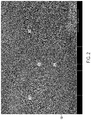
- FIG. 2 is an SEM micrograph showing a perspective view of a cracked bridge waveguide structure overlying a semiconductor substrate
- FIG. 3 is a cross-sectional schematic view of an optical module including an optical fiber aligned to a photonic integrated circuit (PIC) die;
- PIC photonic integrated circuit
- FIG. 4 is a cross-sectional SEM micrograph of a bridge waveguide structure overlying a semiconductor substrate, an optical fiber located proximate to the bridge waveguide structure, and a layer of composite adhesive disposed between the bridge waveguide structure and the substrate;
- FIG. 5 is a perspective schematic view of a plurality of optical fibers located within grooves formed in a PIC die proximate to a bridge waveguide structure following the formation of a layer of a composite adhesive between the bridge waveguide structure and the PIC die;
- FIG. 6 is a perspective schematic view of a plurality of optical fibers located within grooves formed in a PIC die proximate to a bridge waveguide structure following the incorporation of a fill material and an optical adhesive between the bridge waveguide structure and the PIC die.
- a scanning electron microscope (SEM) micrograph depicts a portion of a comparative optical module.
- the optical module includes a substrate (e.g., chip) 100 and a bridge waveguide structure 120 contiguous with and extending over the substrate 100 .
- the bridge waveguide structure 120 is adapted to function as an optical waveguide, i.e., a suspended waveguide.
- a layer of adhesive 200 is disposed within cavity 240 between the bridge waveguide structure 120 and the substrate 100 .
- a crack 122 is formed in and extends through the bridge waveguide structure 120 .
- the crack 122 creates discontinuity in the waveguide and adversely affects performance of the optical module.
- a reflow process may include heating the substrate 100 from room temperature (e.g., 25° C.) to a target temperature of 180-300° C. at a heating rate of 25° C./min, maintaining the target temperature for a dwell time of 60-120 seconds, and cooling the substrate to 25° C. at a cooling rate of 25° C./min.
- substrate 100 may define a portion of a photonics chip, and may include a semiconductor material such as silicon, e.g., single crystal Si or polycrystalline Si, or a silicon-containing material.
- Silicon-containing materials include, but are not limited to, single crystal silicon germanium (SiGe), polycrystalline silicon germanium, silicon doped with carbon (Si:C), amorphous Si, as well as combinations and multi-layers thereof.
- SiGe single crystal silicon germanium
- Si:C silicon doped with carbon
- amorphous Si as well as combinations and multi-layers thereof.
- the term “single crystal” denotes a crystalline solid, in which the crystal lattice of the entire solid is substantially continuous and substantially unbroken to the edges of the solid with substantially no grain boundaries.
- the semiconductor substrate 100 may include (100)-oriented silicon or (111)-oriented silicon, for example.
- the substrate 100 is not limited to silicon-containing materials, however, as the substrate 100 may include other semiconductor materials, including Ge and compound semiconductors, including III-V compound semiconductors such as GaAs, InAs, GaN, GaP, InSb, ZnSe, and ZnS, and II-VI compound semiconductors such as CdSe, CdS, CdTe, ZnSe, ZnS and ZnTe.
- III-V compound semiconductors such as GaAs, InAs, GaN, GaP, InSb, ZnSe, and ZnS
- II-VI compound semiconductors such as CdSe, CdS, CdTe, ZnSe, ZnS and ZnTe.
- Substrate 100 may be a bulk substrate or a composite substrate such as a semiconductor-on-insulator (SOI) substrate that includes, from bottom to top, a handle portion, an isolation layer (e.g., buried oxide layer), and a semiconductor material layer (e.g., silicon).
- SOI semiconductor-on-insulator
- the bridge waveguide structure 120 is plate-shaped and may include one or more apertures 124 extending therethrough.
- apertures 124 may be substantially circular or oval and have a diameter of 5 to 15 microns. Apertures 124 may be formed using conventional photolithography and etching techniques.
- Bridge waveguide structure 120 may be formed using a selective, anisotropic etch process.
- Example methods of forming bridge waveguide structure 120 leverage a difference in the etch rate of materials having different compositions, or a difference in the etch rate of different crystal planes in a given crystalline material. For instance, when single crystal silicon (Si) is etched, the etch rate along densely-packed directions, e.g., ⁇ 111> directions, may be less than the etch rate along ⁇ 100> and ⁇ 110> directions. This etch rate anisotropy can be used to selectively etch a layer or region having one crystallographic orientation relative to a neighboring layer or region having a different crystallographic orientation.
- a bridge layer is formed over semiconductor substrate 100 .
- the composition and/or crystalline habit of the bridge layer are chosen such that the underlying substrate can be etched selectively with respect to the bridge layer, e.g., through apertures 124 , to form a cavity 240 between the bridge layer and the substrate and thereby reveal a bridge waveguide structure 120 .
- bridge waveguide structure 120 extends horizontally over substrate 100 and, by way of example, may be cantilevered, i.e., supported at 1, 2 or 3 (out of four) sides.
- cavity 240 can be formed by etching away a portion of the substrate 100 beneath the bridge layer.
- the bridge layer and therefore the bridge waveguide structure 120 includes a waveguiding layer material, such as an oxide material or a polymeric material.
- a waveguiding layer material such as an oxide material or a polymeric material.
- An oxide material may include silicon dioxide, for example.
- the waveguiding layer material has a lower refractive index than the semiconductor substrate.
- An example bridge waveguide structure 120 has a thickness of 5 to 20 microns, e.g., 5, 10, 15 or 20 microns, including ranges between any of the foregoing values.
- a depth of the cavity 240 measured from the bridge waveguide structure 120 to the substrate 100 , may range from 50 to 200 microns, e.g., 50, 100, 150 or 200 microns, including ranges between any of the foregoing values.
- a selective etch may include an etch chemistry that removes a first material selectively to a second material by a ratio of 2:1 or greater, e.g., 5:1, 10:1 or 20:1.
- horizontal refers to a general direction along a primary surface of a substrate
- vertical is a direction generally orthogonal thereto.
- vertical and horizontal are generally perpendicular directions relative to one another independent of orientation of the substrate in three-dimensional space.
- an optical system wherein an optical component such as an optical fiber is axially aligned to a bridge waveguide structure 120 .
- an optical system includes a substrate 100 having a bridge waveguide structure 120 disposed over the substrate 100 , and an optical fiber 300 aligned with the bridge waveguide structure 120 .
- Substrate 100 may be a photonic integrated circuit (PIC) die.
- PIC photonic integrated circuit
- a photonic integrated circuit (PIC) or integrated optical circuit is a device that integrates multiple photonic functions.
- the optical fiber 300 may include a center core 310 , cladding 320 and an insulating jacket 330 .
- an optical fiber that is “aligned,” “axially aligned,” or “optically aligned” with a bridge waveguide structure is configured to transmit, i.e., send or receive, an optical signal to or from the bridge waveguide structure.
- An upper surface of the chip 100 may be machined or etched to include multiple, parallel V-grooves 105 .
- the V-grooves 105 in the chip 100 may be aligned with additional V-grooves 405 that are similarly formed in an adjacent V-groove block 400 .
- the V-groove block 400 which may be omitted, provides additional support for the fiber(s).
- the optical fiber 300 is positioned within a V-groove 105 formed in the substrate 100 and is aligned to the bridge waveguide structure 120 so that optical signals can be transmitted between the optical fiber 300 and the photonics chip 100 .
- the photonics chip 100 may include a diode or a diode array, for example, configured to convert light into electrical energy or vice versa.
- optical fiber may refer to the combination of the center core 310 , cladding layer 320 and insulating jacket 330 , or to the combination of the center core 310 and the cladding 320 in examples where the insulating jacket is removed.
- the insulating jacket 330 is removed from the optical fiber 300 along the portions thereof where the optical fiber is disposed within the V-grooves 105 , 405 .
- both the insulating jacket 330 and the cladding 320 may be removed along portions of the optical fiber that are disposed within the V-grooves.
- an optical fiber, including a center core 310 and a cladding layer 320 may have a diameter of 100 to 200 microns.
- the optical fiber 300 is positioned within co-linear V-grooves formed in both the V-groove block 400 and the substrate 100 , and is thereby aligned with bridge waveguide structure 120 .
- the optical fiber 300 When an optical fiber 300 is placed in the V-grooves 105 , 405 , the optical fiber 300 may extend above an upper surface of the substrate 100 and/or an upper surface of the V-groove block, the optical fiber 300 may be fully recessed below respective upper surfaces of the substrate 100 and the V-groove block 400 , or a top surface of the optical fiber 300 may be co-planar with a top surface of the substrate 100 and/or a top surface of the V-groove block 400 .
- the substrate 100 and the V-groove block 400 each overlie a carrier 10 , such as a printed circuit board, and may be affixed thereto by respective die attach adhesive layers 102 , 402 .
- a strain relief adhesive layer 302 may be used to secure fiber 300 directly to the carrier 10 .
- a layer of optical adhesive 200 is disposed within V-grooves 105 between the optical fiber 300 and the substrate 100 , and within V-grooves 405 between the optical fiber 300 and the V-groove block 400 such that the relative positions between these components are fixed.
- the optical adhesive 200 may include a polymer resin, for example, such as a UV- or thermally-curable epoxy resin.
- Example resins may be characterized by one or more of a refractive index of 1.3 to 1.6, e.g., 1.3, 1.4, 1.45, 1.5, 1.55 or 1.6, including ranges between any of the foregoing values, a viscosity (at 23° C.) of 200 to 600 cP, a glass transition temperature (T g ) of 0° C.
- an optical transmittance (at 1.3 microns) of at least 85%, e.g., 85, 88, 90, 92 or 94%, including ranges between any of the foregoing values, and a bond strength of 100 to 200 kgf/cm 2 .
- a cover plate 500 is disposed over the fiber(s) 300 and secured using the layer of optical adhesive 200 .
- a single cover plate 500 is disposed over portions of the V-groove block 400 and over portions of the substrate 100 .
- a separate cover plates may be disposed over respective ones of the V-groove block 400 and the substrate 100 .
- the cover plate 500 may be made from any material adapted to provide structural support and hold the fibers 300 within the grooves 105 , 405 .
- An example cover plate is formed from a glass composition.
- Cover plate 500 may be a glass plate, for example.
- optical fibers are disposed within V-grooves between the cover plate 500 and the substrate 100 , and the cover plate 500 is used to ensure that the fibers contact the sidewalls of the V-grooves 105 , 405 and are properly aligned therein.
- a composite adhesive 205 is used to fill the cavity 240 between the bridge waveguide structure 120 and the substrate 100 , and optionally to secure optical fibers 300 within respective V-grooves 105 , 405 .
- the composite adhesive 205 contacts both the bridge waveguide structure 120 and the underlying substrate 100 and is adapted to support the bridge waveguide structure 120 .
- the composite adhesive 205 includes a polymer or resin 210 and a filler 215 .
- the resin 210 may include an adhesive composition such as a curable (e.g., UV-curable or thermally-curable) epoxy acrylate or other suitable material.
- Example filler materials include low coefficient of thermal expansion (CTE) particles and fibers, such as silica particles, e.g., fumed silica particles, and fibers of molybdenum or tungsten, although other low CTE filler materials are contemplated.
- a further filler material 215 is air, i.e., air-filled pores dispersed throughout the resin 210 .
- a pore-containing composite adhesive may be formed by aerating a suitable resin.
- a composite adhesive 205 which includes a filler 215 , is distinct from an optical adhesive 200 .
- Particulate fillers may have a particle (or pore) size of 10 nanometers to 10 microns, e.g., 10, 20, 50, 100, 200, 500, 1000, 2000, 5000 or 10000 nm, including ranges between any of the foregoing values. Fibrous fillers may be characterized by a diameter and a length.
- Example fibrous fillers have a diameter of 10 nanometers to 10 microns, e.g., 10, 20, 50, 100, 200, 500, 1000, 2000, 5000 or 10000 nm, including ranges between any of the foregoing values, and a length of 20 nm to 100 microns, e.g., 20, 50, 100, 200, 500, 1000, 2000, 5000, 10000, 20000, 50000 or 100000 nm, including ranges between any of the foregoing values.
- Example resins 210 may have a coefficient of thermal expansion at 23° C. of 50 ⁇ 10 ⁇ 6 to 200 ⁇ 10 ⁇ 6 /° C., e.g., 50 ⁇ 10 ⁇ 6 , 80 ⁇ 10 ⁇ 6 , 100 ⁇ 10 ⁇ 6 , 150 ⁇ 10 ⁇ 6 or 200 ⁇ 10 ⁇ 6 /° C., including ranges between any of the foregoing values, while the filler material 215 may have a coefficient of thermal expansion at 23° C. of 0.5 ⁇ 10 ⁇ 6 /° C.
- the composite adhesive 205 dispersed within cavity 240 may include a physical mixture of the resin 210 and the filler 215 .
- the filler 215 may be homogeneously or non-homogeneously distributed throughout the resin 210 .
- Example composite adhesives 205 include up to 95 vol. % filler, e.g., 5, 10, 20, 30, 40, 50, 60, 70 80, 90 or 95 vol. %, including ranges between any of the foregoing values.
- the composite adhesive material 205 is a multi-phase, e.g., 2-phase mixture.
- the resin 210 and the filler 215 may be disposed within cavity 240 as separate, unmixed layers.
- the filler 215 may include low CTE particles or fibers that are added to cavity 240 independent of the resin 210 .
- the filler 215 may occupy up to 95% of the cavity volume, e.g., 5, 10, 20, 30, 40, 50, 60, 70, 80, 90 or 95 vol. %, including ranges between any of the foregoing values.
- the composite adhesive 205 has a coefficient of thermal expansion (CTE) less than that of the resin alone.
- the composite adhesive is configured to have a CTE that is comparable to the CTE of the bridge waveguide structure 120 .
- the coefficient of thermal expansion of the composite adhesive material 205 at 23° C. may range from 5 ⁇ 10 ⁇ 6 /° C. to 40 ⁇ 10 ⁇ 6 /° C., e.g., 5 ⁇ 10 ⁇ 6 , 10 ⁇ 10 ⁇ 6 , 15 ⁇ 10 ⁇ 6 , 20 ⁇ 10 ⁇ 6 , 30 ⁇ 10 ⁇ 6 or 40 ⁇ 10 ⁇ 6 /° C., including ranges between any of the foregoing values.
- the effective CTE of the composite adhesive within cavity 240 can be controlled.
- the composite adhesive material 205 may be dispensed into cavity 240 to fill the cavity.
- the composite adhesive material 205 may be dispensed to fill or substantially fill the cavity 240 beneath the bridge waveguide structure 120 .
- a composite adhesive material 205 that fills at least 90% by volume of a cavity 240 e.g., 90, 95, 98, 99 or 100 vol. %, including ranges between any of the foregoing values, “substantially fills” the cavity.
- the composite adhesive material 205 may initially be sufficiently fluid so as to readily fill cavity 240 and optionally the interstices between the optical fiber 300 and the V-grooves 105 , 405 . As shown schematically in FIG. 3 , a layer of the composite adhesive material 205 may also be formed over a top surface of the bridge waveguide structure 120 . In embodiments where a composite adhesive is disposed both over a top surface of the bridge waveguide structure and between the bridge waveguide structure and the substrate, the respective layers of composite adhesive may have the same or comparable coefficients of thermal expansion, i.e., coefficients of thermal expansion that differ by less than 10%, e.g., less than 10, 5, 2 or 1%, including ranges between any of the foregoing values.
- the composite adhesive disposed over a top surface of the bridge waveguide structure may include the same resin and/or the same filler as the composite adhesive disposed between the bridge waveguide structure and the substrate.
- the composite adhesive is disposed over a sidewall of the bridge waveguide structure, i.e., between the top and bottom surfaces of the bridge waveguide structure.
- a composite adhesive material 205 may be dispensed into cavity 240 between the bridge waveguide structure 120 and the substrate, as well as within V-grooves 105 , 405 to secure the optical fiber 300 .
- a composite adhesive material 205 may be dispensed into cavity 240 between the bridge waveguide structure 120 and the substrate, while an adhesive composition 200 not containing a filler may be deposited within V-grooves 105 , 405 to secure the optical fiber.
- An adhesive not containing a filler may be deposited between the distal end of the optical fiber and the bridge waveguide structure 120 .
- the composite adhesive material may be dispensed using a suitable dispense system, such as a micro fluid dispense system marketed by Nordson (East Buffalo, R.I.).
- a suitable dispense system such as a micro fluid dispense system marketed by Nordson (East Buffalo, R.I.).
- An example dispense system may include portable or bench-top dispense system that is operable to a pressurize and deliver through a dispensing tip an effective amount of a composite adhesive material to a desired location on an optical system, e.g., using a 3-axis micromanipulator for controlling the tip location.
- the CTE of the resulting composite adhesive 205 may be decreased relative to the resin alone, such that the impact of thermal cycling of an optical system having the composite adhesive 205 incorporated into the cavity 240 beneath a bridge waveguide structure 120 does not result in the formation of a crack 122 in the bridge waveguide structure 120 .
- FIG. 4 shown is a cross-sectional SEM micrograph of a bridge waveguide structure 120 overlying a semiconductor substrate 100 , and an optical fiber 300 positioned within V-groove 105 .
- a layer of composite adhesive 205 is disposed within cavity 240 between the bridge waveguide structure 120 and the substrate 100
- a layer of optical adhesive 200 is disposed within groove 105 between the fiber 300 and the substrate 100 .
- FIG. 5 is a perspective schematic view of an optical system including a plurality of optical fibers 300 located within respective grooves 105 in substrate 100 and axially aligned with a bridge waveguide structure 120 formed in the substrate 100 .
- a glass cover plate 500 is disposed over the fibers 300 .
- a layer of optical adhesive 200 is disposed within grooves 105 between the fibers 300 and the substrate 100 and between the substrate 100 and the cover plate 500 .
- a layer of composite adhesive 205 is disposed within cavity 240 between the bridge waveguide structure 120 and the substrate 100 .
- the composite adhesive 205 includes a homogeneous mixture of filler material particles 215 , e.g., fumed silica particles, and resin 210 .
- FIG. 6 is a perspective schematic view of an optical system according to further embodiments.
- the optical system and includes a plurality of optical fibers 300 disposed within grooves 105 in substrate 100 and axially aligned with a bridge waveguide structure 120 .
- a glass cover plate 500 is disposed over the fibers 300 .
- a layer of optical adhesive 200 is disposed within grooves 105 between the fibers 300 and the substrate 100 and between the substrate 100 and the cover plate 500 .
- a composite adhesive 205 is disposed within the cavity 240 between the bridge waveguide structure 120 and the substrate 100 .
- the composite adhesive 205 includes a layer of resin 210 overlying a plurality of low CTE fibers 215 .
- the composite adhesive 205 may include a layer of resin 210 and a layer of a low CTE filler material, such as a low CTE glass composition.
- the refractive index (n) of the composite adhesive material 205 may be adapted to facilitate low loss, refractive index matching between the optical fiber 300 and the bridge waveguide structure 120 .
- the composite adhesive material 205 may have a refractive index equal to, or substantially equal to, a portion of the bridge waveguide structure 120 .
- a first value is “substantially equal to” a second value if the first value differs from the second value by 10% or less, e.g., 0, 1, 2, 5, or 10%, including ranges between any of the foregoing values.
- the composite adhesive material 205 may have a refractive index of 1.3 to 1.6, e.g., 1.3, 1.4, 1.45, 1.5, 1.55 or 1.6, including ranges between any of the foregoing values. That is, in certain embodiments, the composite adhesive material 205 may be characterized by a refractive index of 1.3 to 1.6 after curing.
- an optical system includes a photonics chip including a bridge waveguide structure, and an optical fiber disposed over the chip and optically aligned with the bridge waveguide structure.
- a cavity between the bridge waveguide structure and the chip is at least partially filled with an adhesive resin and a filler material having a coefficient of thermal expansion less than that of the adhesive resin.
- the composite adhesive material may include filler particles dispersed throughout the adhesive resin, or a discrete later of material separate from the adhesive resin.
- the composite material filling the cavity has an effective coefficient of thermal expansion less than the coefficient of thermal expansion of conventional adhesive resins, which improves the survivability of the overlying bridge waveguide structure following thermal cycling of the optical system.
- fill material or an “optical fiber” includes examples having two or more such “filler materials” or two or more such “optical fibers” unless the context clearly indicates otherwise.
Landscapes
- Physics & Mathematics (AREA)
- General Physics & Mathematics (AREA)
- Optics & Photonics (AREA)
- Chemical & Material Sciences (AREA)
- Crystallography & Structural Chemistry (AREA)
- Optical Couplings Of Light Guides (AREA)
- Optical Integrated Circuits (AREA)
Abstract
Description
Claims (20)
Priority Applications (2)
| Application Number | Priority Date | Filing Date | Title |
|---|---|---|---|
| US16/000,011 US10520679B2 (en) | 2018-06-05 | 2018-06-05 | Fiber alignment to photonics chip |
| TW108115387A TWI706572B (en) | 2018-06-05 | 2019-05-03 | Methods and structures for fiber alignment to photonics chip |
Applications Claiming Priority (1)
| Application Number | Priority Date | Filing Date | Title |
|---|---|---|---|
| US16/000,011 US10520679B2 (en) | 2018-06-05 | 2018-06-05 | Fiber alignment to photonics chip |
Publications (2)
| Publication Number | Publication Date |
|---|---|
| US20190369339A1 US20190369339A1 (en) | 2019-12-05 |
| US10520679B2 true US10520679B2 (en) | 2019-12-31 |
Family
ID=68692911
Family Applications (1)
| Application Number | Title | Priority Date | Filing Date |
|---|---|---|---|
| US16/000,011 Active US10520679B2 (en) | 2018-06-05 | 2018-06-05 | Fiber alignment to photonics chip |
Country Status (2)
| Country | Link |
|---|---|
| US (1) | US10520679B2 (en) |
| TW (1) | TWI706572B (en) |
Families Citing this family (7)
| Publication number | Priority date | Publication date | Assignee | Title |
|---|---|---|---|---|
| JP7103059B2 (en) * | 2018-08-24 | 2022-07-20 | 日本電信電話株式会社 | Optical module |
| US11209598B2 (en) * | 2019-02-28 | 2021-12-28 | International Business Machines Corporation | Photonics package with face-to-face bonding |
| US12153325B2 (en) * | 2020-04-22 | 2024-11-26 | Nippon Telegraph And Telephone Corporation | Wavelength converter |
| US20240069287A1 (en) * | 2021-02-26 | 2024-02-29 | Intel Corporation | Novel design for fiber array unit (fau) for optical transceiver products |
| US20240178207A1 (en) * | 2022-11-28 | 2024-05-30 | Intel Corporation | Photonic integrated circuit packages including substrates with glass cores |
| US12474519B2 (en) * | 2023-05-26 | 2025-11-18 | Globalfoundries U.S. Inc. | Photonics chip patterning with multiple photoresist layers |
| US20250044534A1 (en) * | 2023-07-31 | 2025-02-06 | Ayar Labs, Inc. | Direct Silicon-to-Silicon Bonding for Fiber-First Packaging Process |
Citations (5)
| Publication number | Priority date | Publication date | Assignee | Title |
|---|---|---|---|---|
| US5787214A (en) * | 1995-05-06 | 1998-07-28 | Bookham Technology Ltd. | Connection between an integrated optical waveguide and an optical fibre |
| US20040214377A1 (en) | 2003-04-28 | 2004-10-28 | Starkovich John A. | Low thermal expansion adhesives and encapsulants for cryogenic and high power density electronic and photonic device assembly and packaging |
| US20070292086A1 (en) * | 2006-06-19 | 2007-12-20 | Nielson Jeffrey D | Hard coating on rugged vee groove connectors |
| US9129986B2 (en) | 2013-06-28 | 2015-09-08 | Globalfoundries Inc. | Spacer chamfering for a replacement metal gate device |
| US20170293073A1 (en) * | 2016-04-08 | 2017-10-12 | Acacia Communications, Inc. | Filling a cavity through a reservoir and a feed-channel and related apparatus and methods |
Family Cites Families (2)
| Publication number | Priority date | Publication date | Assignee | Title |
|---|---|---|---|---|
| US6882790B2 (en) * | 2002-09-25 | 2005-04-19 | Sumitomo Electric Industries, Ltd. | Optical fiber array and substrate for the optical fiber array |
| US9720171B2 (en) * | 2012-06-19 | 2017-08-01 | Sumitomo Bakelite Co., Ltd. | Optical waveguide, optical interconnection component, optical module, opto-electric hybrid board, and electronic device |
-
2018
- 2018-06-05 US US16/000,011 patent/US10520679B2/en active Active
-
2019
- 2019-05-03 TW TW108115387A patent/TWI706572B/en active
Patent Citations (5)
| Publication number | Priority date | Publication date | Assignee | Title |
|---|---|---|---|---|
| US5787214A (en) * | 1995-05-06 | 1998-07-28 | Bookham Technology Ltd. | Connection between an integrated optical waveguide and an optical fibre |
| US20040214377A1 (en) | 2003-04-28 | 2004-10-28 | Starkovich John A. | Low thermal expansion adhesives and encapsulants for cryogenic and high power density electronic and photonic device assembly and packaging |
| US20070292086A1 (en) * | 2006-06-19 | 2007-12-20 | Nielson Jeffrey D | Hard coating on rugged vee groove connectors |
| US9129986B2 (en) | 2013-06-28 | 2015-09-08 | Globalfoundries Inc. | Spacer chamfering for a replacement metal gate device |
| US20170293073A1 (en) * | 2016-04-08 | 2017-10-12 | Acacia Communications, Inc. | Filling a cavity through a reservoir and a feed-channel and related apparatus and methods |
Non-Patent Citations (1)
| Title |
|---|
| Kolari, K.,"High Etch Selectivity for Plasma Etching SiO2 with AlN and Al2O3 Masks"; Microelectronic Engineering 85 (2008) pp. 985-987. |
Also Published As
| Publication number | Publication date |
|---|---|
| TW202005103A (en) | 2020-01-16 |
| US20190369339A1 (en) | 2019-12-05 |
| TWI706572B (en) | 2020-10-01 |
Similar Documents
| Publication | Publication Date | Title |
|---|---|---|
| US10520679B2 (en) | Fiber alignment to photonics chip | |
| US12271032B2 (en) | Integrated optical waveguides, direct-bonded waveguide interface joints, optical routing and interconnects | |
| US12546957B2 (en) | Photonic integrated circuit packaging architectures | |
| US12321022B2 (en) | Apparatus for optical fiber-to-photonic chip connection and associated methods | |
| US10416380B1 (en) | Suspended photonic waveguides with top side sealing | |
| US10564352B1 (en) | Photonic integrated circuit bonded with interposer | |
| CN105372757B (en) | Method for fabricating integrated optical circuits | |
| US6975798B2 (en) | Waveguides assembled for transverse-transfer of optical power | |
| US20210173145A1 (en) | Structures and methods for aligning and securing optical fibers in photonic integrated circuit (pic) packages using various adhesives | |
| CN114616655A (en) | Wafer level fabrication of optical devices | |
| US20040071388A1 (en) | Heat sink for a planar waveguide substrate | |
| KR102903332B1 (en) | Optical engine including fiber deflection unit and method forming the same | |
| CN120167083A (en) | Photonic integrated circuit package including a substrate having a glass core | |
| US20260072225A1 (en) | Optical devices and methods of manufacture | |
| US20240176070A1 (en) | Photonic integrated circuit packages including substrates with glass cores | |
| CN118732155A (en) | Optical input/output interface between photonic chips | |
| US20240176069A1 (en) | Photonic integrated circuit packages including substrates with glass cores | |
| CN111624708B (en) | CMOS process compatible longitudinal optical coupling system and method thereof | |
| US20090074350A1 (en) | Electrically pluggable optical interconnect | |
| CN222354102U (en) | Optical device | |
| CN223217705U (en) | Device structure and components | |
| TWI919053B (en) | Method of manufacturing a packaging structure and a packaging structure | |
| TWI916838B (en) | Optical devices and methods of manufacture | |
| US20250355203A1 (en) | Co-packaged optical fiber mounting unit and method of fabrication | |
| EP1540397B1 (en) | Waveguides assembled for transverse-transfer of optical power |
Legal Events
| Date | Code | Title | Description |
|---|---|---|---|
| FEPP | Fee payment procedure |
Free format text: ENTITY STATUS SET TO UNDISCOUNTED (ORIGINAL EVENT CODE: BIG.); ENTITY STATUS OF PATENT OWNER: LARGE ENTITY |
|
| AS | Assignment |
Owner name: GLOBALFOUNDRIES INC., CAYMAN ISLANDS Free format text: ASSIGNMENT OF ASSIGNORS INTEREST;ASSIGNORS:KNICKERBOCKER, SARAH;LUBGUBAN, JORGE;TONG, TRACY;SIGNING DATES FROM 20180524 TO 20180604;REEL/FRAME:046379/0989 |
|
| STCF | Information on status: patent grant |
Free format text: PATENTED CASE |
|
| AS | Assignment |
Owner name: GLOBALFOUNDRIES U.S. INC., CALIFORNIA Free format text: ASSIGNMENT OF ASSIGNORS INTEREST;ASSIGNOR:GLOBALFOUNDRIES INC.;REEL/FRAME:054633/0001 Effective date: 20201022 |
|
| AS | Assignment |
Owner name: GLOBALFOUNDRIES U.S. INC., NEW YORK Free format text: RELEASE BY SECURED PARTY;ASSIGNOR:WILMINGTON TRUST, NATIONAL ASSOCIATION;REEL/FRAME:056987/0001 Effective date: 20201117 Owner name: GLOBALFOUNDRIES U.S. INC., NEW YORK Free format text: RELEASE OF SECURITY INTEREST;ASSIGNOR:WILMINGTON TRUST, NATIONAL ASSOCIATION;REEL/FRAME:056987/0001 Effective date: 20201117 |
|
| MAFP | Maintenance fee payment |
Free format text: PAYMENT OF MAINTENANCE FEE, 4TH YEAR, LARGE ENTITY (ORIGINAL EVENT CODE: M1551); ENTITY STATUS OF PATENT OWNER: LARGE ENTITY Year of fee payment: 4 |