US10476015B2 - Organic electronic/optoelectronic devices - Google Patents
Organic electronic/optoelectronic devices Download PDFInfo
- Publication number
- US10476015B2 US10476015B2 US15/740,611 US201615740611A US10476015B2 US 10476015 B2 US10476015 B2 US 10476015B2 US 201615740611 A US201615740611 A US 201615740611A US 10476015 B2 US10476015 B2 US 10476015B2
- Authority
- US
- United States
- Prior art keywords
- additive
- organic material
- semiconductive organic
- molecular
- semiconductive
- Prior art date
- Legal status (The legal status is an assumption and is not a legal conclusion. Google has not performed a legal analysis and makes no representation as to the accuracy of the status listed.)
- Active, expires
Links
- 230000005693 optoelectronics Effects 0.000 title abstract description 10
- 239000000654 additive Substances 0.000 claims abstract description 160
- 230000000996 additive effect Effects 0.000 claims abstract description 131
- 239000004065 semiconductor Substances 0.000 claims abstract description 121
- XLYOFNOQVPJJNP-UHFFFAOYSA-N water Substances O XLYOFNOQVPJJNP-UHFFFAOYSA-N 0.000 claims abstract description 80
- 239000011368 organic material Substances 0.000 claims abstract description 58
- 230000000694 effects Effects 0.000 claims abstract description 17
- 239000002800 charge carrier Substances 0.000 claims abstract description 13
- 239000000463 material Substances 0.000 claims description 33
- 239000002904 solvent Substances 0.000 claims description 27
- 238000012360 testing method Methods 0.000 claims description 19
- QVGXLLKOCUKJST-UHFFFAOYSA-N atomic oxygen Chemical compound [O] QVGXLLKOCUKJST-UHFFFAOYSA-N 0.000 claims description 16
- 239000001301 oxygen Substances 0.000 claims description 16
- 229910052760 oxygen Inorganic materials 0.000 claims description 16
- 239000007787 solid Substances 0.000 claims description 10
- 238000010348 incorporation Methods 0.000 claims description 8
- 239000007788 liquid Substances 0.000 claims description 8
- 238000009835 boiling Methods 0.000 claims description 6
- 230000008859 change Effects 0.000 claims description 6
- 239000010410 layer Substances 0.000 description 68
- 239000010408 film Substances 0.000 description 46
- 239000004020 conductor Substances 0.000 description 30
- 229920000642 polymer Polymers 0.000 description 21
- 238000002474 experimental method Methods 0.000 description 19
- IJGRMHOSHXDMSA-UHFFFAOYSA-N Atomic nitrogen Chemical compound N#N IJGRMHOSHXDMSA-UHFFFAOYSA-N 0.000 description 18
- IXHWGNYCZPISET-UHFFFAOYSA-N 2-[4-(dicyanomethylidene)-2,3,5,6-tetrafluorocyclohexa-2,5-dien-1-ylidene]propanedinitrile Chemical compound FC1=C(F)C(=C(C#N)C#N)C(F)=C(F)C1=C(C#N)C#N IXHWGNYCZPISET-UHFFFAOYSA-N 0.000 description 16
- 229920006254 polymer film Polymers 0.000 description 16
- 238000012546 transfer Methods 0.000 description 16
- 230000006872 improvement Effects 0.000 description 15
- 239000002019 doping agent Substances 0.000 description 12
- 238000000034 method Methods 0.000 description 12
- 238000000137 annealing Methods 0.000 description 10
- NLZUEZXRPGMBCV-UHFFFAOYSA-N Butylhydroxytoluene Chemical compound CC1=CC(C(C)(C)C)=C(O)C(C(C)(C)C)=C1 NLZUEZXRPGMBCV-UHFFFAOYSA-N 0.000 description 9
- 238000005259 measurement Methods 0.000 description 9
- 239000013557 residual solvent Substances 0.000 description 9
- 229910052757 nitrogen Inorganic materials 0.000 description 8
- 239000011148 porous material Substances 0.000 description 8
- 230000009286 beneficial effect Effects 0.000 description 7
- 238000006243 chemical reaction Methods 0.000 description 7
- 238000000151 deposition Methods 0.000 description 7
- 238000011084 recovery Methods 0.000 description 7
- 229910021580 Cobalt(II) chloride Inorganic materials 0.000 description 6
- GVPFVAHMJGGAJG-UHFFFAOYSA-L cobalt dichloride Chemical compound [Cl-].[Cl-].[Co+2] GVPFVAHMJGGAJG-UHFFFAOYSA-L 0.000 description 6
- 230000007613 environmental effect Effects 0.000 description 6
- 239000000203 mixture Substances 0.000 description 6
- 238000004402 ultra-violet photoelectron spectroscopy Methods 0.000 description 6
- -1 9,9-di-n-octylfluorenyl-2,7-diyl Chemical group 0.000 description 5
- 238000005338 heat storage Methods 0.000 description 5
- 238000004519 manufacturing process Methods 0.000 description 5
- 230000009456 molecular mechanism Effects 0.000 description 5
- 238000003860 storage Methods 0.000 description 5
- MYMOFIZGZYHOMD-UHFFFAOYSA-N Dioxygen Chemical compound O=O MYMOFIZGZYHOMD-UHFFFAOYSA-N 0.000 description 4
- CTQNGGLPUBDAKN-UHFFFAOYSA-N O-Xylene Chemical group CC1=CC=CC=C1C CTQNGGLPUBDAKN-UHFFFAOYSA-N 0.000 description 4
- 239000003570 air Substances 0.000 description 4
- 230000015556 catabolic process Effects 0.000 description 4
- 238000006731 degradation reaction Methods 0.000 description 4
- 230000008021 deposition Effects 0.000 description 4
- 229910001882 dioxygen Inorganic materials 0.000 description 4
- 238000000572 ellipsometry Methods 0.000 description 4
- 238000002161 passivation Methods 0.000 description 4
- 150000005839 radical cations Chemical class 0.000 description 4
- VYPSYNLAJGMNEJ-UHFFFAOYSA-N silicon dioxide Inorganic materials O=[Si]=O VYPSYNLAJGMNEJ-UHFFFAOYSA-N 0.000 description 4
- 150000003384 small molecules Chemical class 0.000 description 4
- 239000000126 substance Substances 0.000 description 4
- 239000011800 void material Substances 0.000 description 4
- PBKONEOXTCPAFI-UHFFFAOYSA-N 1,2,4-trichlorobenzene Chemical compound ClC1=CC=C(Cl)C(Cl)=C1 PBKONEOXTCPAFI-UHFFFAOYSA-N 0.000 description 3
- RFFLAFLAYFXFSW-UHFFFAOYSA-N 1,2-dichlorobenzene Chemical compound ClC1=CC=CC=C1Cl RFFLAFLAYFXFSW-UHFFFAOYSA-N 0.000 description 3
- OCJBOOLMMGQPQU-UHFFFAOYSA-N 1,4-dichlorobenzene Chemical compound ClC1=CC=C(Cl)C=C1 OCJBOOLMMGQPQU-UHFFFAOYSA-N 0.000 description 3
- YXFVVABEGXRONW-UHFFFAOYSA-N Toluene Chemical compound CC1=CC=CC=C1 YXFVVABEGXRONW-UHFFFAOYSA-N 0.000 description 3
- 238000004458 analytical method Methods 0.000 description 3
- 230000004888 barrier function Effects 0.000 description 3
- 239000003990 capacitor Substances 0.000 description 3
- 239000013078 crystal Substances 0.000 description 3
- 229940117389 dichlorobenzene Drugs 0.000 description 3
- 238000006056 electrooxidation reaction Methods 0.000 description 3
- 238000011049 filling Methods 0.000 description 3
- 230000003993 interaction Effects 0.000 description 3
- 229910052751 metal Inorganic materials 0.000 description 3
- 239000002184 metal Substances 0.000 description 3
- 238000012545 processing Methods 0.000 description 3
- 238000003380 quartz crystal microbalance Methods 0.000 description 3
- 235000012239 silicon dioxide Nutrition 0.000 description 3
- 238000000859 sublimation Methods 0.000 description 3
- 230000008022 sublimation Effects 0.000 description 3
- 239000000758 substrate Substances 0.000 description 3
- CXWXQJXEFPUFDZ-UHFFFAOYSA-N tetralin Chemical compound C1=CC=C2CCCCC2=C1 CXWXQJXEFPUFDZ-UHFFFAOYSA-N 0.000 description 3
- QPUYECUOLPXSFR-UHFFFAOYSA-N 1-methylnaphthalene Chemical compound C1=CC=C2C(C)=CC=CC2=C1 QPUYECUOLPXSFR-UHFFFAOYSA-N 0.000 description 2
- LNXVNZRYYHFMEY-UHFFFAOYSA-N 2,5-dichlorocyclohexa-2,5-diene-1,4-dione Chemical compound ClC1=CC(=O)C(Cl)=CC1=O LNXVNZRYYHFMEY-UHFFFAOYSA-N 0.000 description 2
- 229920001621 AMOLED Polymers 0.000 description 2
- 239000004593 Epoxy Substances 0.000 description 2
- 239000003849 aromatic solvent Substances 0.000 description 2
- 230000015572 biosynthetic process Effects 0.000 description 2
- MVPPADPHJFYWMZ-UHFFFAOYSA-N chlorobenzene Chemical compound ClC1=CC=CC=C1 MVPPADPHJFYWMZ-UHFFFAOYSA-N 0.000 description 2
- 229920000547 conjugated polymer Polymers 0.000 description 2
- 230000001627 detrimental effect Effects 0.000 description 2
- 238000009792 diffusion process Methods 0.000 description 2
- 229910001873 dinitrogen Inorganic materials 0.000 description 2
- 238000009826 distribution Methods 0.000 description 2
- 238000003487 electrochemical reaction Methods 0.000 description 2
- 238000005538 encapsulation Methods 0.000 description 2
- 230000001747 exhibiting effect Effects 0.000 description 2
- 238000000605 extraction Methods 0.000 description 2
- 230000002349 favourable effect Effects 0.000 description 2
- PCHJSUWPFVWCPO-UHFFFAOYSA-N gold Chemical compound [Au] PCHJSUWPFVWCPO-UHFFFAOYSA-N 0.000 description 2
- 239000010931 gold Substances 0.000 description 2
- 229910052737 gold Inorganic materials 0.000 description 2
- 230000005524 hole trap Effects 0.000 description 2
- 239000001257 hydrogen Substances 0.000 description 2
- 229910052739 hydrogen Inorganic materials 0.000 description 2
- 230000007935 neutral effect Effects 0.000 description 2
- 229940078552 o-xylene Drugs 0.000 description 2
- 239000000843 powder Substances 0.000 description 2
- 239000010453 quartz Substances 0.000 description 2
- 238000011160 research Methods 0.000 description 2
- 238000001228 spectrum Methods 0.000 description 2
- FHCPAXDKURNIOZ-UHFFFAOYSA-N tetrathiafulvalene Chemical compound S1C=CSC1=C1SC=CS1 FHCPAXDKURNIOZ-UHFFFAOYSA-N 0.000 description 2
- 239000010409 thin film Substances 0.000 description 2
- LQXFOLBBQWZYNH-UHFFFAOYSA-N 2-[6-(dicyanomethylidene)-1,3,4,5,7,8-hexafluoronaphthalen-2-ylidene]propanedinitrile Chemical compound FC1=C(F)C(=C(C#N)C#N)C(F)=C2C(F)=C(F)C(=C(C#N)C#N)C(F)=C21 LQXFOLBBQWZYNH-UHFFFAOYSA-N 0.000 description 1
- YBAZINRZQSAIAY-UHFFFAOYSA-N 4-aminobenzonitrile Chemical compound NC1=CC=C(C#N)C=C1 YBAZINRZQSAIAY-UHFFFAOYSA-N 0.000 description 1
- 239000005964 Acibenzolar-S-methyl Substances 0.000 description 1
- 238000004566 IR spectroscopy Methods 0.000 description 1
- XOJVVFBFDXDTEG-UHFFFAOYSA-N Norphytane Natural products CC(C)CCCC(C)CCCC(C)CCCC(C)C XOJVVFBFDXDTEG-UHFFFAOYSA-N 0.000 description 1
- 108010059332 Photosynthetic Reaction Center Complex Proteins Proteins 0.000 description 1
- 238000001069 Raman spectroscopy Methods 0.000 description 1
- VWLPSQFSQSEILZ-UHFFFAOYSA-N S1C=CC=C1.S1C=CC=C1.[Mo] Chemical compound S1C=CC=C1.S1C=CC=C1.[Mo] VWLPSQFSQSEILZ-UHFFFAOYSA-N 0.000 description 1
- RTAQQCXQSZGOHL-UHFFFAOYSA-N Titanium Chemical compound [Ti] RTAQQCXQSZGOHL-UHFFFAOYSA-N 0.000 description 1
- 238000004833 X-ray photoelectron spectroscopy Methods 0.000 description 1
- 239000011358 absorbing material Substances 0.000 description 1
- 238000009825 accumulation Methods 0.000 description 1
- 230000002411 adverse Effects 0.000 description 1
- 239000012080 ambient air Substances 0.000 description 1
- 150000001454 anthracenes Chemical class 0.000 description 1
- 230000008901 benefit Effects 0.000 description 1
- WGQKYBSKWIADBV-UHFFFAOYSA-N benzylamine Chemical compound NCC1=CC=CC=C1 WGQKYBSKWIADBV-UHFFFAOYSA-N 0.000 description 1
- 230000003197 catalytic effect Effects 0.000 description 1
- 238000012512 characterization method Methods 0.000 description 1
- 229910052681 coesite Inorganic materials 0.000 description 1
- 229920001577 copolymer Polymers 0.000 description 1
- 229910052906 cristobalite Inorganic materials 0.000 description 1
- 150000001924 cycloalkanes Chemical class 0.000 description 1
- 238000000354 decomposition reaction Methods 0.000 description 1
- 230000005516 deep trap Effects 0.000 description 1
- 230000002950 deficient Effects 0.000 description 1
- 230000000593 degrading effect Effects 0.000 description 1
- 230000001419 dependent effect Effects 0.000 description 1
- 238000011161 development Methods 0.000 description 1
- 238000010586 diagram Methods 0.000 description 1
- 230000009977 dual effect Effects 0.000 description 1
- 239000000945 filler Substances 0.000 description 1
- 239000004811 fluoropolymer Substances 0.000 description 1
- 229920002313 fluoropolymer Polymers 0.000 description 1
- 239000011521 glass Substances 0.000 description 1
- 238000010438 heat treatment Methods 0.000 description 1
- 238000004770 highest occupied molecular orbital Methods 0.000 description 1
- 239000012535 impurity Substances 0.000 description 1
- 230000001939 inductive effect Effects 0.000 description 1
- 230000010354 integration Effects 0.000 description 1
- 230000007774 longterm Effects 0.000 description 1
- 238000004949 mass spectrometry Methods 0.000 description 1
- 239000011159 matrix material Substances 0.000 description 1
- 230000007246 mechanism Effects 0.000 description 1
- 230000008018 melting Effects 0.000 description 1
- 238000002844 melting Methods 0.000 description 1
- AUHZEENZYGFFBQ-UHFFFAOYSA-N mesitylene Substances CC1=CC(C)=CC(C)=C1 AUHZEENZYGFFBQ-UHFFFAOYSA-N 0.000 description 1
- 125000001827 mesitylenyl group Chemical group [H]C1=C(C(*)=C(C([H])=C1C([H])([H])[H])C([H])([H])[H])C([H])([H])[H] 0.000 description 1
- 150000002739 metals Chemical class 0.000 description 1
- 238000004776 molecular orbital Methods 0.000 description 1
- 238000012544 monitoring process Methods 0.000 description 1
- UNFUYWDGSFDHCW-UHFFFAOYSA-N monochlorocyclohexane Chemical compound ClC1CCCCC1 UNFUYWDGSFDHCW-UHFFFAOYSA-N 0.000 description 1
- 230000003287 optical effect Effects 0.000 description 1
- 239000012044 organic layer Substances 0.000 description 1
- XLYOFNOQVPJJNP-UHFFFAOYSA-O oxonium Chemical compound [OH3+] XLYOFNOQVPJJNP-UHFFFAOYSA-O 0.000 description 1
- 238000012856 packing Methods 0.000 description 1
- 230000037361 pathway Effects 0.000 description 1
- 230000008569 process Effects 0.000 description 1
- 230000009467 reduction Effects 0.000 description 1
- 239000013074 reference sample Substances 0.000 description 1
- 239000002094 self assembled monolayer Substances 0.000 description 1
- 239000013545 self-assembled monolayer Substances 0.000 description 1
- 230000035945 sensitivity Effects 0.000 description 1
- 239000000377 silicon dioxide Substances 0.000 description 1
- 229910052682 stishovite Inorganic materials 0.000 description 1
- 238000003786 synthesis reaction Methods 0.000 description 1
- PCCVSPMFGIFTHU-UHFFFAOYSA-N tetracyanoquinodimethane Chemical compound N#CC(C#N)=C1C=CC(=C(C#N)C#N)C=C1 PCCVSPMFGIFTHU-UHFFFAOYSA-N 0.000 description 1
- 239000010936 titanium Substances 0.000 description 1
- 229910052719 titanium Inorganic materials 0.000 description 1
- FMZQNTNMBORAJM-UHFFFAOYSA-N tri(propan-2-yl)-[2-[13-[2-tri(propan-2-yl)silylethynyl]pentacen-6-yl]ethynyl]silane Chemical compound C1=CC=C2C=C3C(C#C[Si](C(C)C)(C(C)C)C(C)C)=C(C=C4C(C=CC=C4)=C4)C4=C(C#C[Si](C(C)C)(C(C)C)C(C)C)C3=CC2=C1 FMZQNTNMBORAJM-UHFFFAOYSA-N 0.000 description 1
- 229910052905 tridymite Inorganic materials 0.000 description 1
Images


Classifications
-
- H—ELECTRICITY
- H10—SEMICONDUCTOR DEVICES; ELECTRIC SOLID-STATE DEVICES NOT OTHERWISE PROVIDED FOR
- H10K—ORGANIC ELECTRIC SOLID-STATE DEVICES
- H10K10/00—Organic devices specially adapted for rectifying, amplifying, oscillating or switching; Organic capacitors or resistors having potential barriers
- H10K10/40—Organic transistors
- H10K10/46—Field-effect transistors, e.g. organic thin-film transistors [OTFT]
- H10K10/462—Insulated gate field-effect transistors [IGFETs]
- H10K10/484—Insulated gate field-effect transistors [IGFETs] characterised by the channel regions
-
- H01L51/0558—
-
- H01L51/0003—
-
- H01L51/0007—
-
- H01L51/002—
-
- H—ELECTRICITY
- H10—SEMICONDUCTOR DEVICES; ELECTRIC SOLID-STATE DEVICES NOT OTHERWISE PROVIDED FOR
- H10K—ORGANIC ELECTRIC SOLID-STATE DEVICES
- H10K10/00—Organic devices specially adapted for rectifying, amplifying, oscillating or switching; Organic capacitors or resistors having potential barriers
- H10K10/40—Organic transistors
- H10K10/46—Field-effect transistors, e.g. organic thin-film transistors [OTFT]
- H10K10/462—Insulated gate field-effect transistors [IGFETs]
- H10K10/464—Lateral top-gate IGFETs comprising only a single gate
-
- H—ELECTRICITY
- H10—SEMICONDUCTOR DEVICES; ELECTRIC SOLID-STATE DEVICES NOT OTHERWISE PROVIDED FOR
- H10K—ORGANIC ELECTRIC SOLID-STATE DEVICES
- H10K71/00—Manufacture or treatment specially adapted for the organic devices covered by this subclass
- H10K71/10—Deposition of organic active material
- H10K71/12—Deposition of organic active material using liquid deposition, e.g. spin coating
- H10K71/15—Deposition of organic active material using liquid deposition, e.g. spin coating characterised by the solvent used
-
- H—ELECTRICITY
- H10—SEMICONDUCTOR DEVICES; ELECTRIC SOLID-STATE DEVICES NOT OTHERWISE PROVIDED FOR
- H10K—ORGANIC ELECTRIC SOLID-STATE DEVICES
- H10K71/00—Manufacture or treatment specially adapted for the organic devices covered by this subclass
- H10K71/30—Doping active layers, e.g. electron transporting layers
-
- H01L51/0541—
Definitions
- organic devices Electronic/optoelectronic devices based on organic semiconductors (hereafter referred to as “organic devices”) are increasingly attracting interest for more and more applications because of the high on-currents and good on-off ratios increasingly achievable in organic semiconductor films deposited from solution at low temperatures and the inherently flexible, mechanical properties of organic semiconductors which enable electronics in flexible form factors.
- the inventors for the present application have found that the performance stability (i.e. stress and environmental stability) of organic devices can be relatively poor, and an aim of the present invention is to provide a technique by which the performance stability of an organic device can be improved.
- an electronic or optoelectronic device including a semiconductor layer, wherein the semiconductor layer comprises at least a semiconductive organic material, water species, and at least one additive in an amount of at least 0.1% by weight relative to the semiconductive organic material, which additive at least partly negates a charge carrier trapping effect caused by the water species on the semiconductive organic material.
- an electronic or optoelectronic device including a semiconductor layer, wherein the semiconductor layer comprises at least a semiconductive organic material, and at least one additive in an amount of at least 0.1% by weight relative to the semiconductive organic material, which additive occupies at least some voids within the semiconductive organic material occupiable by water molecules, and has a smaller charge carrier trapping effect on the semiconductive organic material than water.
- a method of producing an electronic or optoelectronic device comprising forming a stack of layers including a semiconductor layer comprising a semiconductive organic material, wherein forming said stack of layers comprises depositing at least one molecular additive material that at least partly negates a charge carrier trapping effect caused by water molecules on the semiconductive organic material; and retaining the additive in said stack to an extent that the molecular additive exists in the semiconductor layer in an amount of at least 0.1% by weight relative to the semiconductive organic material.
- a method of producing an electronic or optoelectronic device comprising forming a stack of layers including a semiconductor layer comprising a semiconductive organic material, wherein forming said stack of layers comprises depositing at least one molecular additive material that occupies at least some voids within the semiconductive organic material occupiable by water molecules, and has a smaller charge carrier trapping effect on the semiconductive organic material than water; and retaining the additive in said stack to an extent that the molecular additive exists in the semiconductor layer in an amount of at least 0.1% by weight relative to the semiconductive organic material.
- said device is an electronic switching device.
- the at least one additive reduces the threshold voltage change of the electron switching device to less than 1V (preferably less than 0.7V) in a stress test involving operating the electronic switching device in a saturation regime at a drain current of about 2.5 ⁇ A for a period of 25 hours.
- the additive comprises molecules having a size less than 5 nm, more preferably less than 2 nm, and further more preferably less than 1 nm.
- the electronic switching device is a p-type semiconductor device
- the additive comprises a material having an electron affinity less than the ionization potential of the semiconductive organic material by at least 0.1 eV, more preferably by at least 0.3 eV, and more preferably by at least 0.5 eV.
- the additive shifts the threshold voltage by no more than 2 V, more preferably by no more than 1V and most preferably by no more than 0.3V.
- the additive reduces the organic semi-conductor mobility by no more than 20%, preferably by no more than 5%, and most preferably by no more than 2%.
- the additive increases the transistor off current by no more than 10 ⁇ , preferably by no more than 5 ⁇ , and most preferably by no more than than 1.2 ⁇ .
- the electronic switching device is a p-type semiconductor device
- the additive comprises a material having an ionization potential greater than the ionization potential of the semiconductive organic material by more than at least 0.3 eV, more preferably by more than at least 0.5 eV, and further more preferably by more than at least 1 eV.
- the additive comprises a molecular material having a molecular weight of less than 5% of the number average molecular weight of the semiconductive organic material, preferably less than 3% and most preferably less than 1%.
- the additive has a higher solubility at room temperature in the organic semiconductive material than water has in the organic semiconductive material.
- the additive has a solubility of at least 0.1% in water.
- the semiconductor layer comprises residual water molecules in an amount of at least 0.1% by weight.
- the semiconductor layer is encapsulated together with one or more other layers of the device against the ingress of oxygen.
- said molecular additive is liquid at room temperature and is a solvent for the semiconductive organic material, wherein the solubility of the semiconductive organic material in the liquid molecular additive is at least 0.1% by weight.
- the boiling point of said additive is higher than 150° C., preferably higher than 180° C. and most preferably higher than 200° C.
- said molecular additive is solid at room temperature and has a solid solubility higher than 1% by weight in the semiconductive organic material.
- the incorporation of the molecular additive reduces the threshold voltage shift of the electronic switching device in a stress test by 50% compared to that of a reference device, in which no molecular additive is incorporated in said semiconductive organic material, wherein said stress test involves operating the device in the saturation regime at a drain current of about (0.25 ⁇ A ⁇ W/L) for a period of 25 hours, where W and L are the channel width and channel length of the electronic switching device.
- the incorporation of said additive in said semiconductive organic material does not significantly increase the OFF-current of the electronic switching device.
- the amount of said additive is at least 1% by weight relative to the semiconductive organic material.
- said semiconductive organic material comprises a polymer.
- said additive is a solvent used to deposit the semiconductive organic material.
- the method comprises depositing said additive as part of a mixture for a layer of said stack other than the semiconductor layer.
- the method comprises retaining the additive in said stack to an extent that the additive exists in the semiconductor layer in an amount of at least 1% by weight relative to the semiconductive organic material.
- FIG. 1 is a schematic drawing of one example of an organic transistor.
- FIG. 2 is a schematic drawing of another example of an organic transistor integrated together with an organic light-emitting device whose output is controlled by the organic transistor.
- FIGS. 3( a ) to 3( e ) show experimental results indicating the improved environmental stability and device uniformity upon incorporation of various additives into the semiconducting film of a p-channel organic transistor.
- FIGS. 4( a ) and 4( b ) show the results of an experiment involving measuring the transistor characteristics at different times during a high temperature storage (HTS) test of another example transistor according to an embodiment of the present invention, and a reference transistor.
- HTS high temperature storage
- FIG. 5 shows the results of an experiment involving the extraction of the threshold voltage at different times both during a stress test and during a subsequent recovery period of transistors according to one embodiment of the present invention and a reference transistor.
- the stresses are performed in a nitrogen environment on transistors with various additives incorporated in the semiconductor.
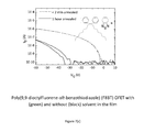
- FIG. 6 compares Ultraviolet Photoelectron Spectroscopy (UPS) data of IDTBT films with F4TCNQ (left) and TCNQ (right) added at levels of 0, 1, 2, 5, 10 and 20%.
- the extracted shift in Fermi level is shown in the top panels whereas the experimental UPS spectra for all films are shown in the bottom panel respectively.
- FIGS. 7 a ) to e ) show experimental results indicating improved performance and stability for as-cast devices as compared to annealed devices. The performance enhancement is observed throughout a wide class of polymers. 7 ( a ) and ( b ) show this for IDTBT, ( c ) shows this for F8BT, and ( d ) and ( e ) show this for DPP-DTT.
- FIG. 8 a ) and b ) show ellipsometry measurements on unannealed and annealed IDTBT films indicating the amount of liquid additive (solvent) present in the polymer film.
- FIG. 9 a ) and b ) show results indicating that poor device performance is caused by water. Removal of water from the device leads to a significant increase in device performance and stability.
- FIG. 10 shows the chemical structures of some examples of solid additives according to the present invention.
- top-gate organic transistors but the same technique is equally applicable to other types of transistors such as bottom-gate transistors or dual gate transistors and other types of electronic/optoelectronic devices.
- a non-limiting, example of a top-gate organic transistor is defined by a stack of layers supported on a rigid or flexible support substrate 2 .
- the stack of layers includes a conductor layer defining source and drain electrodes 4 , 6 ; a semiconductor layer 8 defining a semiconductor channel between the source and drain electrodes; a further conductor layer defining a gate electrode 12 capacitively coupled to the semiconductor channel via a gate dielectric layer 10 ; an electrically-insulating passivation layer 14 formed over the gate electrode; and yet a further conductor layer defining a pixel electrode 16 connected to the drain electrode through a via-hole 18 formed in the stack.
- the stack may be encapsulated against the ingress of oxygen by encapsulating films 17 .
- Each layer may comprise a respective stack of sub-layers.
- the conductor layer defining the source and drain electrodes 4 , 6 may comprise a lower sub-layer of a material exhibiting good adhesion to the surface of the underlying support substrate, and an upper sub-layer of a material exhibiting a better electrical conductivity than the material of the lower sub-layer.
- the organic transistor may also comprise additional elements; for example, the organic transistor may include a self-assembled monolayer of organic material on the upper surface of the source and drain electrodes 4 . 6 to better facilitate the transfer of charge carriers between the source/drain electrodes 4 , 6 and the semiconductor 8 .
- FIG. 1 only shows one transistor but a typical transistor device comprises an array of transistors in which: (a) the lower conductor layer defines an array of source conductors each providing the source electrodes for a respective line of transistors and connected to a respective terminal of a source driver chip, and an array of drain conductors each providing the drain electrode for a respective transistor; (b) the second conductor layer defines an array of gate lines each providing the gate electrodes for a respective column of transistors and each connected to a respective terminal of a gate driver chip; and (c) the third conductor layer defines an array of pixel electrodes each connected to a drain conductor of a respective transistor.
- the electric potential at each pixel electrode can be controlled independently because each transistor is associated with a unique combination of source conductor and gate line.
- AMOLEDs active matrix organic light-emitting display devices
- the optical output of pixels of an organic light-emitting material are controlled by respective transistors (or respective sets of transistors).
- the semiconductor layer (along with other elements of the device such as oxygen-sensitive elements comprising reactive metals) may be encapsulated against the ingress of oxygen; which encapsulation is shown schematically in FIG. 1 .
- each pixel is associated with at least 2 respective transistors and a respective memory element in the form of a capacitor (referred to as 2T1C).
- the source driver chip is connected to the source conductor 26 of the switch transistor (secondary TFT); and the gate driver chip is connected to the gate conductor 22 of the switch transistor (secondary TFT).
- the drain conductor 28 of the switch TFT (secondary TFT) is connected to the gate conductor 24 of the drive TFT (primary TFT); the source conductor 30 of the drive TFT (primary TFT) is connected to a power supply Vdd; and the drain conductor 32 of the drive TFT (primary TFT) is connected to the respective pixel electrode 16 .
- the capacitor mentioned above is formed between the gate conductor 24 of the drive TFT and the source conductor 30 of the drive TFT (primary TFT).
- the circuitry for each pixel can also contain compensation circuits. A large variety of compensation circuits exist having four to seven TFTs and one or more capacitors. These compensation circuits can compensate for a shift in the threshold voltage of the light-emitting device (e.g.
- FIG. 2 additionally shows the integration of an organic light-emitting device including a layer of light-emissive material 18 , and a common electrode 20 formed over the layer of light-emissive material serving as the counter electrode to the pixel electrode 16 .
- the pixel electrode may form the cathode of the light-emitting device and the common electrode 20 may form the anode of the light-emitting device.
- encapsulating films 17 may be provided if other layers of the stack do not already encapsulate the semiconductor and any other oxygen-sensitive elements against the ingress of molecular oxygen.
- the organic transistor may also comprise additional elements, and one or more layers may comprise a stack of sub-layers.
- FIG. 2 only shows one pixel but an AMOLED typically comprises an array of thousands or millions of pixels in which (for the specific example of top-gate transistors shown in FIG. 2 ): (a) the lower conductor layer defines an array of source conductors each providing the source electrodes of the switch TFTs for a respective line of pixels and each connected to a respective terminal of a source driver chip, an array of drain conductors each providing the drain electrode for a respective pixel, and one or more conductors providing the source electrodes for the drive TFTs; (b) the second conductor layer defines an array of gate lines each providing the gate electrodes of the switch TFTs for a respective column of pixels and each connected to a respective terminal of a gate driver chip, and an array of gate conductors each providing the gate electrode of the drive TFT of a respective pixel; and (c) the third conductor layer defines an array of pixel electrodes each connected to a drain conductor of the drive TFT of a respective pixel. Again, the current through the light-emissive material
- a first experiment involved measuring the transistor characteristic of a transistor after storage in different environments.
- Four different top-gate organic transistors were the subject of the experiment.
- the first was a bottom-contact, top-gate transistor comprising a glass support substrate, source/drain electrodes photolithographically patterned from a conductor layer stack comprising a lower layer of titanium and an upper layer of gold; the poly-indaceno-dithiophene-co-benzothiadiazole (IDTBT) conjugated co-polymer as the organic semiconductor; a CYTOP® fluoropolymer for the gate dielectric; and gold for the gate electrode.
- IDTBT poly-indaceno-dithiophene-co-benzothiadiazole
- the IDTBT conjugated polymer semiconductor was deposited from solution.
- the other transistors were identical in architecture with the exception that 2 wt. % (relative to the polymer) of a small organic molecule was incorporated in solution as an additive.
- This additive will be referred to as a molecular additive in the following.
- the molecular additives are F4-TCNQ (2,3,5,6-tetrafluoro-7,7,8,8-tetracyanoquinodimethane), TCNQ (7,7,8,8-tetracyanoquinodimethane), and ABN (4-Aminobenzonitrile).
- FIG. 3 shows the measured transistor characteristic immediately after manufacture in a nitrogen environment (black line—bottom of set of 4 lines), after 24 hours exposure to air (blue line—top of set of 4 lines), again after a further 24 hours storage in a nitrogen gas environment (red line—2 nd top of set of 4 lines), and finally after annealing overnight in a nitrogen glovebox (green line—2 nd bottom of set of 4 lines), consecutively.
- FIG. 3 a shows these for a pure transistor with no additives.
- the device characteristics depend strongly on the atmosphere in which the device is stored and measured, in particular under condition where no or little oxygen is present, the device characteristics are degraded as evidenced by a sluggish turn-on characteristics.
- FIG. 3 shows the measured transistor characteristic immediately after manufacture in a nitrogen environment (black line—bottom of set of 4 lines), after 24 hours exposure to air (blue line—top of set of 4 lines), again after a further 24 hours storage in a nitrogen gas environment (red line—2 nd top of set of 4 lines), and finally
- FIGS. 3 ( a ) to 3( d ) show these for a transistor with F4-TCNQ as an additive
- FIG. 3 c shows these for a transistor with TCNQ as an additive
- FIG. 3 d shows these for a transistor with ABN as an additive.
- F4-TCNQ is a charge transfer dopant for the organic semiconductor IDTBT, because the electron affinity of F4-TCNQ is close to and possibly even larger than the ionization potential of IDTBT. This should lead to an electron charge transfer from an occupied molecular orbital of the organic semiconductor to an empty molecular orbit of the dopant F4-TCNQ and lead to an undesirable increase in the OFF current of the transistor. This is indeed observable in FIG. 3( b ) where the OFF current of the F4-TCNQ device is on the order of 10 ⁇ 7 A, i.e. 1-2 orders of magnitude higher than that of the pristine IDTBT film ( FIG. 3( a ) ).
- Exposure to oxygen has a similar beneficial effect on the performance and stability of pure IDTBT transistors (without molecular additive, see FIG. 3 a ), but this effect is not permanent and the device degrades again in an oxygen deficient atmosphere.
- the inclusion of molecular oxygen in the host semiconductor is not compatible with the use of the organic transistor in integrated devices including oxygen-sensitive elements, such as the reactive metal cathodes of state-of-the-art electronic light-emitting devices, because the molecular oxygen can migrate from the transistor semiconductor to the oxygen-sensitive elements and degrade their performance.
- the use of additives can achieve the above-described improvement in transistor performance stability without the same risk of degradation to any oxygen-sensitive elements integrated together with the organic transistor.
- a further experiment involved subjecting organic transistors to a heat storage test in a vacuum environment and measuring the transistor characteristic at different times during the heat storage test.
- the heat storage test involved storing the transistor in a vacuum environment (1.7 ⁇ 10 ⁇ 2 mbar) at a temperature of 70° C.
- two types of top-gate organic transistors were the subject of the experiment.
- the first was a transistor comprising an conjugated semiconductor polymer (without any additives) having an ionization potential of 5.3 eV deposited from solution and a SU-8 epoxy-based polymer layer with 7% by weight of a molecular additive 2,5-dichloro-1,4-benzoquinone as additive over the gate electrode and the gate dielectric.
- the second transistor was exactly the same as the first transistor except that the passivation layer over the gate electrode and gate dielectric was did not comprise an additive in the SU-8 epoxy-based polymer layer.
- the first transistor (SU-8 with 2,5-dichloro-1,4-benzoquinone) shows a remarkably small variation in transistor characteristic over the 45 hour duration of the heat storage test, compared to the second transistor (SU-8 passivation layer without additive).
- the molecular additive may not need to be present in the organic semiconductor layer during deposition, but can be introduced into another organic layer in the device stack in close proximity to the organic semiconductor layer, from which it may then diffuse into the organic semiconductor layer.
- Other examples of device elements from which to introduce the molecular additive into the semiconductor are (i) an organic gate dielectric layer and/or (ii) an organic planarisation layer on which the source/drain conductors are formed, in addition to or as an alternative to introducing the additive into the semiconductor from an organic passivation layer deposited over the gate dielectric and gate electrode.
- One or more barrier layers may be provided within the stack of layers that defines the transistors to reduce the diffusion of the additive out from the organic semiconductor layer into one or more other parts of the device.
- these one or more barrier layers may be in addition to one or more barrier layers that protect oxygen-sensitive elements, such as the reactive metal cathodes, against degradation by atmospheric oxygen.
- the inventors for the present application have observed a high variation in the threshold voltage in p-channel organic transistors before and after stress/storage testing of the transistors, particularly in an inert environment, and it has been found by experiment that the threshold voltage stability can be improved by introducing a solid, liquid or gaseous molecular additive into the host organic semiconductor.
- a high threshold voltage stability can be an important requirement for display applications of organic transistors, in particular for applications in OLED displays, in which high threshold voltage stability for the pixel drive transistor is key to maintaining a constant drive current (and thereby constant OLED luminance) for a given electrical input.
- An experiment involved subjecting organic transistors to a stress test in an inert, nitrogen gas environment as well as in ambient air and extracting the threshold voltage at different times during the stress test and also during a subsequent period of recovery in the respective environment.
- the stressing involved shorting the drain and gate electrodes in order to operate the transistor in the saturation regime.
- a drain current of ⁇ 2.5 ⁇ A was applied (as per the testing regime presented in H. Sirringhaus, Advanced Materials, DOI: 10.1002/adma.201304346) for the 25 hour duration of the stress experiment.
- a transfer characteristic was obtained in 5 hour intervals during the stress. After the 25 hour stressing period, the shorting between the drain and gate was removed, as well as the current, and the transfer characteristic was monitored over 21 hours, initially in 5 minute intervals and then in 5 hour intervals, monitoring the transistor's recovery.
- FIG. 5 shows a summary of the change in threshold voltage of IDTBT-based p-channel transistors during a constant-current stress experiment at 2.5 uA between the source and drain electrodes for 25 hours. It also shows the subsequent recovery of the threshold voltage over a 21 hour period with all electrodes grounded.
- the threshold voltage was determined by taking the square root of the saturation transfer curve, and taking a linear fit (and extrapolating) of the graph over a 10V range at sufficiently high voltages. Alternative techniques for determining the threshold voltage may also be used (as discussed in H. Sirringhaus, Advanced Materials, DOI: 10.1002/adma.201304346).
- the transistors shown have various additives, and are compared to a transistor with no additive incorporated. The stresses and recovery were carried out in a nitrogen environment.
- the IDTBT transistors with 2% of molecular additives added show a remarkably small variation in threshold voltage ( ⁇ Vt 0.6-1.5V) over the 25 hour duration of the stress test, compared to the transistor not comprising any additive (pure IDTBT). This is observed not only for F4-TCNQ, but also the additives that cannot act as charge transfer dopants for the organic semiconductor. This shows clearly that the incorporation of a molecular additive that does not act as a charge transfer dopant to the organic semiconductor film can improve not only the environmental stability and contact resistance behaviour, but also the operational stress stability.
- FIG. 6 shows Ultraviolet Photoelectron Spectroscopy (UPS) data of IDTBT films with F4TCNQ (left) and TCNQ (right) added at levels of 0, 1, 2, 5, 10 and 20%.
- the films' Fermi level i.e. the energetic level of charge transport
- the data reveals a noticeable shift in Fermi level when adding F4TCNQ to IDTBT films. There is hence, a clear doping effect observed in such films as explained above on the basis of the molecular energy diagram for F4-TCNQ and IDTBT.
- no shift in Fermi level can be observed.
- TCNQ is not doping IDTBT and hence, there is no active charge transfer from the polymer to the dopant.
- doping can in fact be excluded as the origin of the improved OFET performance and stability.
- FIG. 7 shows experiments on improving device performance and stability by deliberately leaving solvents in the polymer films.
- FIG. 7 ( a ) benchmarks the performance of IDTBT transistors that are annealed for 2 minutes at 100° C. against an IDTBT device that is annealed for 1 hour at the same temperature (black line—lowest line in FIG. 7 a ). Since all solvents that are used have high boiling points >180° C., some even above 200° C., annealing at a relatively low temperature of 100° C. for a short time will leave a significant concentration of residual solvent in the film. The amount of residual solvent in a conjugated polymer under these conditions is on the order of a few weight percent relative to the polymer, as quantified below.
- IDTBT devices with residual solvent in the film perform significantly better than devices with the solvent removed after 1 hour of annealing.
- aromatic solvents such as Chlorobenzene, 1,2, Dichlorobenzene, 1,2,4-Trichlorobenzene, Toluene, o-Xylene and Mesitylene (Structures shown in FIG. 7 ( a ) as well as non-aromatic solvents such as Cycloalkanes (e.g. Chlorocyclohexane)).
- the additives should preferably not degrade transistor performance by inducing a threshold shift, reduce the semi-conductor mobility and or increase the transistor off current.
- FIG. 7 ( b ) shows the change in threshold voltage during constant-current stress and a subsequent recovery period performed in a nitrogen environment.
- the figure highlights the improvement in the constant-current stress stability (at 2.5 uA) when the solvent is left in the semiconducting film.
- An increase in the source-drain current by 2 orders of magnitude (100 uA) still shows a stark improvement in constant-current stress stability when compared to a transistor with a semiconductor that has been annealed for 1 hour to remove all solvent.
- FIG. 7 ( c ) shows that leaving the solvent in the film has the same beneficial effect on poly[(9,9-di-n-octylfluorenyl-2,7-diyl)-alt-(benzo[2,1,3]thiadiazol-4,8-diyl)] (F8BT) transistors.
- the transistors shown are spun from o-xylene and were annealed for 2 minutes and 1 hour, respectively.
- the F8BT transistor annealed for a short time shows orders of magnitude improvements of device performances.
- FIG. 7 ( d ) shows the linear (dashed line) and saturation (continuous line) regime transfer characteristics of two transistors that consist of poly-diketopyrrolopyrrole-co-dithienothiophene (DPP-DTT) as the semiconducting layer, annealed for 2 minutes and 1 hour, respectively.
- the transistors shown are spun from 1,2-dichlorobenzene.
- the transistor with residual solvent shows a dramatic improvement over the one annealed for 1 hour.
- FIG. 7 ( e ) shows the change in threshold voltage during constant-current stress and a subsequent recovery period of DPP-DTT based transistors. The measurement was performed in a nitrogen environment.
- the case where residual solvent is left in the semiconducting film shows a marked improvement over the annealed transistor, both stressed at 2.5 uA.
- the improved stability is maintained even when the source-drain current is increased by an order of magnitude (50 uA).
- FIG. 8 ( a ) shows an ellipsometry measurement of an IDTBT film with the solvent (Dichlorobenzene) deliberately left in the film.
- EMA effective medium approximation
- the results on IDTBT were additionally firmed up by using quartz crystal microbalance (QCM) measurements.
- QCM quartz crystal microbalance
- an IDTBT film was spun on a quartz crystal and annealed for 2 minutes at 100° C.
- the resonance frequency of the crystal was then determined before and after the film was annealed for a further hour at 100° C. Since the resonance frequency of the quartz crystal is linearly dependent on weight, the mass loss of the polymer film during annealing (i.e. the amount of solvent leaving the polymer film) could be identified to be 0.6%. This agrees well with the ellipsometry data from FIGS. 8 ( a ) and ( b ) .
- the same measurement was conducted for IDTBT films with different side chains resulting in a mass loss that varied between 0.6% and 1.5%.
- FIG. 9 ( b ) shows further evidence that the presence of water in the organic host material is the predominant reason for poor performance and stability of polymer transistors.
- FIG. 9 ( b ) shows further evidence that the presence of water in the organic host material is the predominant reason for poor performance and stability of polymer transistors.
- an experiment is shown in which a polymer transistor was stored together with powder of the highly water absorbing material Cobalt(II)Chloride for the duration of 48 hours. The storage was done in a sealed box inside a nitrogen glove box and the transistor was in non-contact with the Cobalt(II)Chloride.
- reaction proceeds all the way as a multi-electron electrochemical oxidation to the evolution of molecular oxygen (as implied by the above reaction), which may require a catalytic environment to bind the various intermediate molecular species in a well-defined molecular geometry (analogous to that present in the photosynthetic reaction center) or whether it proceeds as a single electron reaction that binds the originally mobile positive charge strongly to a water molecule (or to a cluster of water molecules) the result is that the originally mobile charge carrier on the organic semiconductor has been converted into a deeply trapped charge that is no longer able to carry an electronic current.
- the inventors of the present invention also note that the charge trapping process occurring in the presence of water may in fact not involve neutral water molecules, but ionic species that are naturally present within water. For example, depending on the pH of the water a small concentration of negatively charged hydroxyl ions, OH ⁇ , and positively charged hydronium ions, H 3 O + , are present within water. Hydroxyl ions, in particular, could react with the positive hole charge carriers induced on the organic semiconductive polymer in p-type operation mode, which could lead to trapping of the holes on the polymer by formation of hydroxyl radicals .OH. This trapping is likely to be the more prominent the larger the pH of the water source is, from which the water molecules incorporated within the organic semiconductive polymer stem.
- results demonstrated in this disclosure demonstrate that the detrimental effect of residual water in the organic semiconductor can be overcome by incorporating within the organic semiconductor film a small molecular additive that is of a similar molecular size as a water molecule and has an affinity to form a non-covalent bond with the organic semiconductor such that it is readily incorporated into the same nanometer-sized cavities within the organic semiconductor that water is incorporated in.
- the molecular additive is able to perturb the electrochemical reaction between water and the radical cations on the organic semiconductor, such that this reaction is no longer able to proceed efficiently.
- the detailed molecular mechanism by which the additive interacts with the water molecule and with the organic semiconductor is difficult to establish by direct experimental or spectroscopic characterization because of the minute concentrations of molecular species that are involved and is also likely to depend on the type of additive.
- the solvent molecules listed it may, for example, involve an energetically favourable, ⁇ - ⁇ interaction between the organic semiconductor and the solvent molecules that removes direct physical contact between the organic semiconductor and the water molecule, i.e., the solvent molecules insert themselves in between the organic semiconductor and the water molecules. Since the ionization potential of the molecular additives is chosen to be much deeper than that of the organic semiconductor, the positive holes induced in the organic semiconductor remain spatially separated from the water molecules.
- the molecular additive preferably has the following properties:
- the desirable removal of water-related traps in the organic semiconductor by the addition of a molecular additive can be applied to a range of electronic and optoelectronic devices, including, but not limited to, transistors in either planar or vertical architecture, rectifying diodes, light-emitting diodes (LEDs) and solar cells.
- transistors in either planar or vertical architecture rectifying diodes, light-emitting diodes (LEDs) and solar cells.
- LEDs light-emitting diodes
- solar cells solar cells.
- Vertical transistors, LEDs and solar cells rely on charge transport through the bulk of the organic semiconductor as opposed to transport along the interface, which is also highly sensitive to the presence of charge carrier traps. The results shown in FIG.
- the presence of a molecular additive in the polymer film can be detected by a range of analytical techniques known in the prior art. At the concentrations of a few % that are typically needed to fill the voids in the polymer film, a wide range of analytical techniques have sufficient sensitivity, such as X-ray photoelectron spectroscopy, infrared or Raman spectroscopy or various forms of mass spectrometry.
- a particularly sensitive method to detect the presence of the small molecular additive makes use of the fact that typical molecular additives have a lower boiling/sublimation temperature than the decomposition temperature of the polymer. This analysis is performed in three steps: First the composition of the polymer film as it is found in the electronic device is analysed by any of these techniques.
- the polymer film is annealed at a temperature higher than the boiling/sublimation temperature of the molecular additive, but less than the degradation temperature of the polymer.
- the molecular additive is typically removed from the film while the composition of the polymer host remains unchanged.
- the chemical composition of the film is then re-measured. If there are significant differences in chemical composition before and after the annealing step one can conclude that a small molecular additive had been present in the film.
Landscapes
- Engineering & Computer Science (AREA)
- Manufacturing & Machinery (AREA)
- Thin Film Transistor (AREA)
- Electroluminescent Light Sources (AREA)
Abstract
Description
-
- (i) The molecular size of the additive is comparable to that of a water molecule, such that the additive can become incorporated into the small, nanometer-sized pores. The molecular additive should therefore be smaller than preferably 5 nm, more preferably smaller than 2 nm, most preferably smaller than 1 nm. Molecular size is defined here as the distance between the two atoms that are furthest apart within the molecule.
- (ii) For a device operating in p-type mode the electron affinity of the molecular additive is smaller than the ionization potential of the organic semiconductor, such that the incorporation of the additive does not lead to molecular p-type doping of the organic semiconductor and an undesirable increase in OFF current. The electron affinity of the molecular additive is therefore preferably smaller by 0.1 eV than the ionization potential of the organic semiconductor, more preferably smaller than 0.3 eV, most preferably smaller than 0.5 eV. Analogously, for a device operating in n-type mode, the ionization potential of the molecular additive should be higher than the electron affinity of the organic semiconductor, in order to prevent undesirable n-type doping of the organic semiconductor by the molecular additive.
- (iii) The ionization potential of the molecular additive should be larger than that of the organic semiconductor, such that holes induced on the organic semiconductor cannot be injected onto the molecular additive. The ionization potential of the molecular additive should be larger than that of the organic semiconductor preferably by 0.3 eV, more preferably 0.5 eV and most preferably by 1 eV. An analogous criterion applies to the electron affinity of the molecular additive with respect to the electron affinity of the organic semiconductor in the case of devices operating in n-type mode.
- (iv) The weight ratio between the molecular additive and the organic semiconductor in the films is preferably on the order of at least 1%, such that all nanoscale pores/voids can be filled with the additive without the additive degrading the transport properties of the organic semiconductor by interrupting the charge transport pathways in the organic semiconductor. In the case of a solid additive this requires the additive to have a solid solubility of at least 1% in the organic semiconductor.
- (v) The molecular additive has preferably a non-covalent, favourable binding interaction with the organic semiconductor that is comparable in strength or larger than that between the organic semiconductor and water such that the molecular additive is easily incorporated into the nanoscale pores and is able to compete with water for binding sites on the organic semiconductor. This will generally mean that the molecular additive has a higher solubility in the organic semiconductor than water has in the organic semiconductor.
- (vi) Preferably, the molecular additive is also able to undergo a non-covalent hydrogen bonding interaction with water, such that it can perturb the molecular geometry and/or the electron density distribution around the water molecules within the nanoscale pores and in this way suppress the electrochemical oxidation of water in the presence of radical cations on the organic semiconductor. This will generally mean that the molecular additive will exhibit a finite solubility in water, preferably higher than 0.1%.
- (vii) The molecular additive should not degrade the TFT performance by either shifting the threshold voltage by more than 2 V, more preferably not by more than less than 1V, and most preferably not by more than 0.3V. Also the molecular additive should not reduce the organic semi-conductor mobility by more than 20%, more preferably not by more than 5% and most preferably not by more than 2%. Finally the molecular additive should not increase the transistor off current by more than 10×, more preferably by not more than 5× and most preferably by not more than 1.2×.
- (viii) The molecular additive preferably has a high thermal stability within the pores of the organic semi-conductor and does not evaporate or sublime from the pores during heating of the device at temperatures of 30-120° C. that are typical during device manufacture or operation. The melting/sublimation (boiling) temperature of the solid (liquid) organic semi-conductor is preferably chosen to be above the highest temperature reached during device manufacture/operation. The inventors of the present invention have found that the beneficial effect of additives such as TCNQ or F4-TCNQ may be lost when the device is heated above 90-100° C. However, when using slightly larger molecules with still sufficient solubility in the organic semi-conductor but higher thermal stability, such as 2,2′-(perfluoronaphthalene-2,6-diylidene)dimalononitrile (F6-TCNNQ) or, preferably, the non-fluorinated derivative TCNNQ (see
FIG. 10 ), which does not lead to p-type doping due to its low electron affinity, the thermal stability was found to be significantly improved. Even larger additives such as the anthracene derivative TCAQ may also be used.
Claims (17)
Applications Claiming Priority (3)
| Application Number | Priority Date | Filing Date | Title |
|---|---|---|---|
| GB1511375.6A GB2539895B (en) | 2015-06-29 | 2015-06-29 | Organic electronic/optoelectronic devices |
| GB1511375.6 | 2015-06-29 | ||
| PCT/EP2016/065137 WO2017001473A1 (en) | 2015-06-29 | 2016-06-29 | Organic electronic/optoelectronic devices |
Publications (2)
| Publication Number | Publication Date |
|---|---|
| US20180190918A1 US20180190918A1 (en) | 2018-07-05 |
| US10476015B2 true US10476015B2 (en) | 2019-11-12 |
Family
ID=53872368
Family Applications (1)
| Application Number | Title | Priority Date | Filing Date |
|---|---|---|---|
| US15/740,611 Active 2036-07-07 US10476015B2 (en) | 2015-06-29 | 2016-06-29 | Organic electronic/optoelectronic devices |
Country Status (8)
| Country | Link |
|---|---|
| US (1) | US10476015B2 (en) |
| JP (1) | JP7077019B2 (en) |
| KR (1) | KR20180020290A (en) |
| CN (1) | CN107925003B (en) |
| DE (1) | DE112016002930T5 (en) |
| GB (1) | GB2539895B (en) |
| TW (1) | TWI714605B (en) |
| WO (1) | WO2017001473A1 (en) |
Families Citing this family (2)
| Publication number | Priority date | Publication date | Assignee | Title |
|---|---|---|---|---|
| US20210111346A1 (en) * | 2017-03-30 | 2021-04-15 | Georgia Tech Research Corporation | Conjugated polymers with multistage side-chain cleavage |
| GB2567871B (en) * | 2017-10-27 | 2022-02-02 | Flexenable Ltd | Electronic device for pressure sensors |
Citations (4)
| Publication number | Priority date | Publication date | Assignee | Title |
|---|---|---|---|---|
| US20090066223A1 (en) * | 2005-02-21 | 2009-03-12 | Mitsubishi Chemical Corporation | Organic electric field light emitting element and production therefor |
| WO2011087601A1 (en) | 2009-12-22 | 2011-07-21 | Universal Display Corporation | Aromatic solvent comprising compositions for inkjet printing of layers comprising organic semiconductive material |
| WO2012033075A1 (en) | 2010-09-07 | 2012-03-15 | 日本化薬株式会社 | Organic semiconductor material, field-effect transistor, and manufacturing method therefor |
| US20140014934A1 (en) * | 2011-09-26 | 2014-01-16 | Panasonic Corporation | Organic thin-film transistor and method of manufacturing organic thin-film transistor |
Family Cites Families (8)
| Publication number | Priority date | Publication date | Assignee | Title |
|---|---|---|---|---|
| TWI385193B (en) * | 2004-12-07 | 2013-02-11 | Sumitomo Chemical Co | Polymer material and components using the same |
| TWI305203B (en) * | 2005-12-29 | 2009-01-11 | Ind Tech Res Inst | N-type organic semiconductor materials |
| CN102959753B (en) | 2010-06-24 | 2017-10-31 | 巴斯夫欧洲公司 | With improving ON/OFF electric current than the organic field effect tube that is moved with controllable threshold |
| JP6065367B2 (en) * | 2011-06-07 | 2017-01-25 | ソニー株式会社 | Nonaqueous electrolyte battery, battery pack, electronic device, electric vehicle, power storage device, and power system |
| JP6111483B2 (en) | 2012-06-04 | 2017-04-12 | 株式会社Joled | Organic EL element and manufacturing method thereof, organic EL panel, organic EL light emitting device, and organic EL display device |
| US9187493B2 (en) * | 2012-08-14 | 2015-11-17 | Nippon Kayaku Kabushiki Kaisha | Heterocyclic compound and use thereof |
| US9959982B2 (en) * | 2012-09-24 | 2018-05-01 | Konica Minolta, Inc. | Photoelectric conversion element and method for producing the same |
| WO2015018480A1 (en) * | 2013-08-07 | 2015-02-12 | Merck Patent Gmbh | Formulation for the preparation of organic electronic (oe) devices comprising a polymeric binder |
-
2015
- 2015-06-29 GB GB1511375.6A patent/GB2539895B/en active Active
-
2016
- 2016-06-29 DE DE112016002930.6T patent/DE112016002930T5/en active Pending
- 2016-06-29 KR KR1020187002308A patent/KR20180020290A/en not_active Withdrawn
- 2016-06-29 CN CN201680043384.2A patent/CN107925003B/en active Active
- 2016-06-29 JP JP2017568066A patent/JP7077019B2/en active Active
- 2016-06-29 TW TW105120542A patent/TWI714605B/en active
- 2016-06-29 US US15/740,611 patent/US10476015B2/en active Active
- 2016-06-29 WO PCT/EP2016/065137 patent/WO2017001473A1/en not_active Ceased
Patent Citations (4)
| Publication number | Priority date | Publication date | Assignee | Title |
|---|---|---|---|---|
| US20090066223A1 (en) * | 2005-02-21 | 2009-03-12 | Mitsubishi Chemical Corporation | Organic electric field light emitting element and production therefor |
| WO2011087601A1 (en) | 2009-12-22 | 2011-07-21 | Universal Display Corporation | Aromatic solvent comprising compositions for inkjet printing of layers comprising organic semiconductive material |
| WO2012033075A1 (en) | 2010-09-07 | 2012-03-15 | 日本化薬株式会社 | Organic semiconductor material, field-effect transistor, and manufacturing method therefor |
| US20140014934A1 (en) * | 2011-09-26 | 2014-01-16 | Panasonic Corporation | Organic thin-film transistor and method of manufacturing organic thin-film transistor |
Non-Patent Citations (11)
| Title |
|---|
| BJÖRN LÜSSEM, HANS KLEEMANN, DANIEL KASEMANN, FABIAN VENTSCH AND KARL LEO: "Organic Junction Field-Effect Transistor", ADVANCED FUNCTIONAL MATERIALS, WILEY - V C H VERLAG GMBH & CO. KGAA, DE, vol. 24, no. 7, 19 February 2014 (2014-02-19), DE, pages 1011 - 1016, XP001588675, ISSN: 1616-301X, DOI: 10.1002/adfm.201301417 |
| EUNHEE LIM, BYUNG-JUN JUNG, MASAYUKI CHIKAMATSU, REIKO AZUMI, YUJI YOSHIDA, KIYOSHI YASE, LEE-MI DO, HONG-KU SHIM: "Doping effect of solution-processed thin-film transistors based on polyfluorene", JOURNAL OF MATERIALS CHEMISTRY, ROYAL SOCIETY OF CHEMISTRY, GB, vol. 17, no. 14, 1 January 2007 (2007-01-01), GB, pages 1416, XP055301980, ISSN: 0959-9428, DOI: 10.1039/b615720c |
| International Search Report dated Sep. 27, 2016 from the International Bureau in counterpart International application No. PCT/EP2016/065137. |
| LEVERMORE P A, ET AL: "Organic light-emitting diodes based on poly(9,9-dioctylfluorene-co-bithiophene) (F8T2)", ADVANCED FUNCTIONAL MATERIALS, WILEY - V C H VERLAG GMBH & CO. KGAA, DE, vol. 19, no. 6, 24 March 2009 (2009-03-24), DE, pages 950 - 957, XP001521179, ISSN: 1616-301X, DOI: 10.1002/adfm.200801260 |
| Levermore, P., et al., "Organic Light-Emitting Diodes Based on Poly (9,9-dioctylfluorene-co-bithiophene) (F8T2)," Advanced Functional Materials, vol. 19, No. 6, 2009, pp. 950-957 (8 pages), XP001521179. |
| Lim, E., et al., "Doping effect of solution-processed thin-film transistors based on polyfluorene", Journal of Materials Chemistry, vol. 17, No. 14, 2007, pp. 1416-1420 (5 pages), XP055301980. |
| Lüssem, B., et al., "Organic Junction Field-Effect Transistor", Advanced Functional Materials, vol. 24, No. 7, 2014, pp. 1011-1016 (6 pages) XP001588675. |
| MA LIANG; LEE WI; PARK YEONG; KIM JONG; LEE HWA; CHO KILWON: "High performance polythiophene thin-film transistors doped with very small amounts of an electron acceptor", APPLIED PHYSICS LETTERS, A I P PUBLISHING LLC, US, vol. 92, no. 6, 15 February 2008 (2008-02-15), US, pages 063310 - 063310-3, XP012108241, ISSN: 0003-6951, DOI: 10.1063/1.2883927 |
| Ma, L., et al., "High performance polythiophene thin-film transistors doped with very small amounts of an electron acceptor", Applied Physics Letters, vol. 92, No. 6, 2008, 3 pages, XP012108241. |
| Yamagishi, Y., et al., "Organic field-effect transistors with molecularly doped polymer gate buffer layer" Synthetic Metals, vol. 162, No. 21-22, 2012, pp. 1887-1893 (7 pages), XP055301998. |
| YUJI YAMAGISHI, KEI NODA, HIROFUMI YAMADA, KAZUMI MATSUSHIGE: "Organic field-effect transistors with molecularly doped polymer gate buffer layer", SYNTHETIC METALS, ELSEVIER SEQUOIA, LAUSANNE, CH, vol. 162, no. 21-22, 1 December 2012 (2012-12-01), CH, pages 1887 - 1893, XP055301998, ISSN: 0379-6779, DOI: 10.1016/j.synthmet.2012.08.020 |
Also Published As
| Publication number | Publication date |
|---|---|
| CN107925003B (en) | 2022-01-11 |
| GB2539895B (en) | 2020-10-07 |
| WO2017001473A1 (en) | 2017-01-05 |
| KR20180020290A (en) | 2018-02-27 |
| TWI714605B (en) | 2021-01-01 |
| JP7077019B2 (en) | 2022-05-30 |
| JP2018521510A (en) | 2018-08-02 |
| US20180190918A1 (en) | 2018-07-05 |
| DE112016002930T5 (en) | 2018-05-30 |
| GB201511375D0 (en) | 2015-08-12 |
| GB2539895A (en) | 2017-01-04 |
| TW201709583A (en) | 2017-03-01 |
| CN107925003A (en) | 2018-04-17 |
Similar Documents
| Publication | Publication Date | Title |
|---|---|---|
| Gershenson et al. | Colloquium: Electronic transport in single-crystal organic transistors | |
| Rossbauer et al. | Comparative Study of the N‐Type Doping Efficiency in Solution‐processed Fullerenes and Fullerene Derivatives | |
| Zschieschang et al. | Separating the impact of oxygen and water on the long-term stability of n-channel perylene diimide thin-film transistors | |
| Ding et al. | Effect of Oxygen, Moisture and Illumination on the Stability and Reliability of Dinaphtho [2, 3-b: 2′, 3′-f] thieno [3, 2-b] thiophene (DNTT) OTFTs during Operation and Storage | |
| KR20130129926A (en) | Field-effect transistor and manufacturing process thereof | |
| Ford et al. | Fullerene Additives Convert Ambipolar Transport to p‐Type Transport while Improving the Operational Stability of Organic Thin Film Transistors | |
| Howells et al. | Influence of perfluorinated ionomer in PEDOT: PSS on the rectification and degradation of organic photovoltaic cells | |
| Chen et al. | Ambient instability of organic field-effect transistors and their improvement strategies | |
| Nikolka | A perspective on overcoming water-related stability challenges in molecular and hybrid semiconductors | |
| Li et al. | Chemical doping of the organic semiconductor C8‐BTBT‐C8 using an aqueous iodine solution for device mobility enhancement | |
| Lee et al. | Necessity of submonolayer LiF anode interlayers for improved device performance in blue phosphorescent OLEDs | |
| Barreto et al. | Improved performance of organic light-emitting transistors enabled by polyurethane gate dielectric | |
| US10476015B2 (en) | Organic electronic/optoelectronic devices | |
| Soldano et al. | Engineering organic/inorganic alumina-based films as dielectrics for red organic light emitting transistors | |
| Li et al. | Fermi level shifts of organic semiconductor films in ambient air | |
| Chiarella et al. | Interfacial charge doping effect in C8-DNTT/PDIF-CN 2 heterojunction field-effect transistors | |
| Walter et al. | Revealing and Controlling Energy Barriers and Valleys at Grain Boundaries in Ultrathin Organic Films | |
| Talik et al. | In-situ analysis energy level alignment at solution processed HAT (CN) 6/PVK (PVK: TAPC) interface via XPS and UPS | |
| Chu et al. | Improved performance in n-channel organic thin film transistors by nanoscale interface modification | |
| US9349958B2 (en) | Use of zwitterionic molecules for forming a hole or electron transport layer | |
| Papaefthimiou et al. | A photoemission study of the Ooct-OPV5/SiO2/Si (1 1 1) interface: Effect of the SiO2 interlayer thickness | |
| Lee et al. | 68.1: Capacitance‐Voltage Characteristics of Top Emitting Organic Light Emitting Diodes for Mobile Display Application | |
| Yasuda et al. | Diethynyl naphthalene derivatives with high ionization potentials for p-channel and n-channel organic field-effect transistors | |
| Haneef | Dynamics of Charge Carrier Traps in Organic Semiconductors | |
| Von Hauff | Field effect investigations of charge carrier transport in organic semiconductors |
Legal Events
| Date | Code | Title | Description |
|---|---|---|---|
| FEPP | Fee payment procedure |
Free format text: ENTITY STATUS SET TO UNDISCOUNTED (ORIGINAL EVENT CODE: BIG.); ENTITY STATUS OF PATENT OWNER: LARGE ENTITY |
|
| AS | Assignment |
Owner name: FLEXENABLE LIMITED, UNITED KINGDOM Free format text: ASSIGNMENT OF ASSIGNORS INTEREST;ASSIGNORS:SIRRINGHAUS, HENNING;NIKOLKA, MARK;NASRALLAH, IYAD;AND OTHERS;SIGNING DATES FROM 20160729 TO 20180105;REEL/FRAME:045798/0332 Owner name: CAMBRIDGE ENTERPRISE LIMITED, UNITED KINGDOM Free format text: ASSIGNMENT OF ASSIGNORS INTEREST;ASSIGNORS:SIRRINGHAUS, HENNING;NIKOLKA, MARK;NASRALLAH, IYAD;AND OTHERS;SIGNING DATES FROM 20160729 TO 20180105;REEL/FRAME:045798/0332 |
|
| STPP | Information on status: patent application and granting procedure in general |
Free format text: NON FINAL ACTION MAILED |
|
| STPP | Information on status: patent application and granting procedure in general |
Free format text: RESPONSE TO NON-FINAL OFFICE ACTION ENTERED AND FORWARDED TO EXAMINER |
|
| STPP | Information on status: patent application and granting procedure in general |
Free format text: NOTICE OF ALLOWANCE MAILED -- APPLICATION RECEIVED IN OFFICE OF PUBLICATIONS |
|
| STPP | Information on status: patent application and granting procedure in general |
Free format text: PUBLICATIONS -- ISSUE FEE PAYMENT VERIFIED |
|
| STCF | Information on status: patent grant |
Free format text: PATENTED CASE |
|
| AS | Assignment |
Owner name: FLEXENABLE TECHNOLOGY LIMITED, UNITED KINGDOM Free format text: ASSIGNMENT OF ASSIGNORS INTEREST;ASSIGNOR:FLEXENABLE LIMITED (IN ADMINISTRATION);REEL/FRAME:062959/0843 Effective date: 20230306 |
|
| FEPP | Fee payment procedure |
Free format text: MAINTENANCE FEE REMINDER MAILED (ORIGINAL EVENT CODE: REM.); ENTITY STATUS OF PATENT OWNER: LARGE ENTITY |
|
| FEPP | Fee payment procedure |
Free format text: SURCHARGE FOR LATE PAYMENT, LARGE ENTITY (ORIGINAL EVENT CODE: M1554); ENTITY STATUS OF PATENT OWNER: LARGE ENTITY |
|
| MAFP | Maintenance fee payment |
Free format text: PAYMENT OF MAINTENANCE FEE, 4TH YEAR, LARGE ENTITY (ORIGINAL EVENT CODE: M1551); ENTITY STATUS OF PATENT OWNER: LARGE ENTITY Year of fee payment: 4 |