US10473579B2 - Apparatus for inspecting material property of plurality of measurement objects - Google Patents
Apparatus for inspecting material property of plurality of measurement objects Download PDFInfo
- Publication number
- US10473579B2 US10473579B2 US15/981,359 US201815981359A US10473579B2 US 10473579 B2 US10473579 B2 US 10473579B2 US 201815981359 A US201815981359 A US 201815981359A US 10473579 B2 US10473579 B2 US 10473579B2
- Authority
- US
- United States
- Prior art keywords
- measurement
- unit
- light
- measurement object
- optical signal
- Prior art date
- Legal status (The legal status is an assumption and is not a legal conclusion. Google has not performed a legal analysis and makes no representation as to the accuracy of the status listed.)
- Active
Links
Images


Classifications
-
- G—PHYSICS
- G01—MEASURING; TESTING
- G01N—INVESTIGATING OR ANALYSING MATERIALS BY DETERMINING THEIR CHEMICAL OR PHYSICAL PROPERTIES
- G01N21/00—Investigating or analysing materials by the use of optical means, i.e. using sub-millimetre waves, infrared, visible or ultraviolet light
- G01N21/84—Systems specially adapted for particular applications
- G01N21/88—Investigating the presence of flaws or contamination
- G01N21/8851—Scan or image signal processing specially adapted therefor, e.g. for scan signal adjustment, for detecting different kinds of defects, for compensating for structures, markings, edges
-
- G—PHYSICS
- G01—MEASURING; TESTING
- G01N—INVESTIGATING OR ANALYSING MATERIALS BY DETERMINING THEIR CHEMICAL OR PHYSICAL PROPERTIES
- G01N21/00—Investigating or analysing materials by the use of optical means, i.e. using sub-millimetre waves, infrared, visible or ultraviolet light
- G01N21/01—Arrangements or apparatus for facilitating the optical investigation
-
- G—PHYSICS
- G01—MEASURING; TESTING
- G01N—INVESTIGATING OR ANALYSING MATERIALS BY DETERMINING THEIR CHEMICAL OR PHYSICAL PROPERTIES
- G01N21/00—Investigating or analysing materials by the use of optical means, i.e. using sub-millimetre waves, infrared, visible or ultraviolet light
- G01N21/17—Systems in which incident light is modified in accordance with the properties of the material investigated
- G01N21/25—Colour; Spectral properties, i.e. comparison of effect of material on the light at two or more different wavelengths or wavelength bands
- G01N21/251—Colorimeters; Construction thereof
- G01N21/253—Colorimeters; Construction thereof for batch operation, i.e. multisample apparatus
-
- G—PHYSICS
- G01—MEASURING; TESTING
- G01N—INVESTIGATING OR ANALYSING MATERIALS BY DETERMINING THEIR CHEMICAL OR PHYSICAL PROPERTIES
- G01N21/00—Investigating or analysing materials by the use of optical means, i.e. using sub-millimetre waves, infrared, visible or ultraviolet light
- G01N21/84—Systems specially adapted for particular applications
- G01N21/88—Investigating the presence of flaws or contamination
-
- G—PHYSICS
- G01—MEASURING; TESTING
- G01N—INVESTIGATING OR ANALYSING MATERIALS BY DETERMINING THEIR CHEMICAL OR PHYSICAL PROPERTIES
- G01N15/00—Investigating characteristics of particles; Investigating permeability, pore-volume or surface-area of porous materials
- G01N15/10—Investigating individual particles
- G01N15/14—Optical investigation techniques, e.g. flow cytometry
- G01N15/1434—Optical arrangements
-
- G—PHYSICS
- G01—MEASURING; TESTING
- G01N—INVESTIGATING OR ANALYSING MATERIALS BY DETERMINING THEIR CHEMICAL OR PHYSICAL PROPERTIES
- G01N21/00—Investigating or analysing materials by the use of optical means, i.e. using sub-millimetre waves, infrared, visible or ultraviolet light
- G01N21/17—Systems in which incident light is modified in accordance with the properties of the material investigated
-
- G—PHYSICS
- G01—MEASURING; TESTING
- G01N—INVESTIGATING OR ANALYSING MATERIALS BY DETERMINING THEIR CHEMICAL OR PHYSICAL PROPERTIES
- G01N21/00—Investigating or analysing materials by the use of optical means, i.e. using sub-millimetre waves, infrared, visible or ultraviolet light
- G01N21/84—Systems specially adapted for particular applications
- G01N21/88—Investigating the presence of flaws or contamination
- G01N21/8806—Specially adapted optical and illumination features
-
- G—PHYSICS
- G01—MEASURING; TESTING
- G01N—INVESTIGATING OR ANALYSING MATERIALS BY DETERMINING THEIR CHEMICAL OR PHYSICAL PROPERTIES
- G01N21/00—Investigating or analysing materials by the use of optical means, i.e. using sub-millimetre waves, infrared, visible or ultraviolet light
- G01N21/84—Systems specially adapted for particular applications
- G01N21/88—Investigating the presence of flaws or contamination
- G01N21/94—Investigating contamination, e.g. dust
-
- H01L21/67288—
-
- H—ELECTRICITY
- H10—SEMICONDUCTOR DEVICES; ELECTRIC SOLID-STATE DEVICES NOT OTHERWISE PROVIDED FOR
- H10P—GENERIC PROCESSES OR APPARATUS FOR THE MANUFACTURE OR TREATMENT OF DEVICES COVERED BY CLASS H10
- H10P72/00—Handling or holding of wafers, substrates or devices during manufacture or treatment thereof
- H10P72/06—Apparatus for monitoring, sorting, marking, testing or measuring
- H10P72/0616—Monitoring of warpages, curvatures, damages, defects or the like
-
- G—PHYSICS
- G01—MEASURING; TESTING
- G01N—INVESTIGATING OR ANALYSING MATERIALS BY DETERMINING THEIR CHEMICAL OR PHYSICAL PROPERTIES
- G01N15/00—Investigating characteristics of particles; Investigating permeability, pore-volume or surface-area of porous materials
- G01N15/10—Investigating individual particles
- G01N15/14—Optical investigation techniques, e.g. flow cytometry
- G01N2015/1493—Particle size
-
- G—PHYSICS
- G01—MEASURING; TESTING
- G01N—INVESTIGATING OR ANALYSING MATERIALS BY DETERMINING THEIR CHEMICAL OR PHYSICAL PROPERTIES
- G01N21/00—Investigating or analysing materials by the use of optical means, i.e. using sub-millimetre waves, infrared, visible or ultraviolet light
- G01N21/84—Systems specially adapted for particular applications
- G01N2021/8411—Application to online plant, process monitoring
-
- G—PHYSICS
- G01—MEASURING; TESTING
- G01N—INVESTIGATING OR ANALYSING MATERIALS BY DETERMINING THEIR CHEMICAL OR PHYSICAL PROPERTIES
- G01N21/00—Investigating or analysing materials by the use of optical means, i.e. using sub-millimetre waves, infrared, visible or ultraviolet light
- G01N21/84—Systems specially adapted for particular applications
- G01N21/8422—Investigating thin films, e.g. matrix isolation method
- G01N2021/8427—Coatings
-
- G—PHYSICS
- G01—MEASURING; TESTING
- G01N—INVESTIGATING OR ANALYSING MATERIALS BY DETERMINING THEIR CHEMICAL OR PHYSICAL PROPERTIES
- G01N21/00—Investigating or analysing materials by the use of optical means, i.e. using sub-millimetre waves, infrared, visible or ultraviolet light
- G01N21/84—Systems specially adapted for particular applications
- G01N21/88—Investigating the presence of flaws or contamination
- G01N21/95—Investigating the presence of flaws or contamination characterised by the material or shape of the object to be examined
- G01N21/9501—Semiconductor wafers
-
- G—PHYSICS
- G01—MEASURING; TESTING
- G01N—INVESTIGATING OR ANALYSING MATERIALS BY DETERMINING THEIR CHEMICAL OR PHYSICAL PROPERTIES
- G01N2201/00—Features of devices classified in G01N21/00
- G01N2201/06—Illumination; Optics
- G01N2201/063—Illuminating optical parts
- G01N2201/0636—Reflectors
-
- G—PHYSICS
- G01—MEASURING; TESTING
- G01N—INVESTIGATING OR ANALYSING MATERIALS BY DETERMINING THEIR CHEMICAL OR PHYSICAL PROPERTIES
- G01N2201/00—Features of devices classified in G01N21/00
- G01N2201/06—Illumination; Optics
- G01N2201/063—Illuminating optical parts
- G01N2201/0638—Refractive parts
-
- G—PHYSICS
- G01—MEASURING; TESTING
- G01N—INVESTIGATING OR ANALYSING MATERIALS BY DETERMINING THEIR CHEMICAL OR PHYSICAL PROPERTIES
- G01N2201/00—Features of devices classified in G01N21/00
- G01N2201/06—Illumination; Optics
- G01N2201/066—Modifiable path; multiple paths in one sample
- G01N2201/0666—Selectable paths; insertable multiple sources
-
- G—PHYSICS
- G01—MEASURING; TESTING
- G01N—INVESTIGATING OR ANALYSING MATERIALS BY DETERMINING THEIR CHEMICAL OR PHYSICAL PROPERTIES
- G01N2201/00—Features of devices classified in G01N21/00
- G01N2201/08—Optical fibres; light guides
- G01N2201/084—Fibres for remote transmission
Definitions
- the present application relates to an inspection apparatus and, more specifically, to an apparatus for inspecting a material property of a plurality of measurement objects.
- semiconductor devices are manufactured through a fabrication (“fab”) process in which an electric circuit including electric components are formed on a silicon wafer, which is used as a semiconductor substrate.
- fab fabrication
- EDS electrical die sorting
- a package assembly process may then be performed for encapsulating each of the semiconductor devices with an epoxy resin and individualizing the semiconductor devices.
- the fab process generally includes a deposition process by which a film is formed on a semiconductor substrate.
- a chemical mechanical polishing process is performed for smoothing the film.
- a photolithography process is performed for forming a photoresist pattern on the film.
- An etching process is performed for forming the film as a pattern having electric characteristics using the photoresist pattern.
- An ion injection process is performed for injecting a specific ion into a predetermined region of the semiconductor substrate.
- a cleaning process is performed for removing impurities from the semiconductor substrate.
- An inspection process is performed for inspecting a surface of the semiconductor substrate on which the film or pattern is formed.
- Defects of the semiconductor substrate such as foreign substances remaining on the semiconductor substrate, may degrade operation performance and productivity of the semiconductor device.
- An inspection apparatus includes a light source generating a first light.
- a first measurement unit is configured to receive the first light from the light source and direct the first light to a first measurement object.
- a second measurement unit is configured to receive the first light from the light source and direct the first light to a second measurement object which is different from the first measurement object.
- An inspection unit is configured to receive a first optical signal provided from the first measurement unit along a first optical path and inspect the first measurement object using the first optical signal, and to receive a second optical signal provided from the second measurement unit along a second optical path that is different from the first optical path and inspect the second measurement object using the second optical signal.
- a measurement position selection unit is configured to alternately enable the first and second optical paths by adjusting an angle of a reflection mirror.
- An inspection apparatus includes a first measurement unit in which a first measurement object is disposed.
- the first measurement unit comprises a first illumination unit configured to provide a first light to the first measurement object, and a first light receiving unit configured to receive the first light passing through the first measurement object.
- a second measurement unit in which a second measurement object is disposed, comprises a second illumination unit configured to provide a second light to the second measurement object, and a second light receiving unit configured to receive the second light passing through the second measurement object.
- An inspection unit is configured to receive a first optical signal provided from the first measurement unit and inspect the first measurement object therefrom, and to receive a second optical signal provided from the second measurement unit and inspect the second measurement object therefrom.
- a reflection mirror is configured to direct either of the first or second optical signals to the inspection unit.
- a control unit is configured to control a driving unit to adjust an angle of the reflection mirror.
- An inspection apparatus includes a first measurement unit configured to direct a light into a first measurement object.
- a second measurement unit is configured to direct the light into a second measurement object.
- An inspection unit is configured to inspect the first measurement object and inspect the second measurement object.
- a measurement position selection unit is configured to alternatively provide a first optical signal from the first measurement unit to the inspection unit and a second optical signal from the second measurement unit to the inspection unit, by adjusting an angle of a reflection mirror.
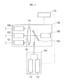
- FIG. 1 is a schematic diagram illustrating an apparatus for inspecting a material property according to some exemplary embodiments of the present disclosure
- FIG. 2 is a flow chart illustrating a method for inspecting a material property using an apparatus for inspecting a material property according to some exemplary embodiments of the present disclosure
- FIG. 3 to FIG. 5 are diagrams illustrating an operation of an apparatus for inspecting a material property according to some exemplary embodiments of the present disclosure
- FIG. 6 is a schematic diagram illustrating an apparatus for inspecting a material property according to some exemplary embodiments of the present disclosure
- FIG. 7 is a schematic diagram illustrating an apparatus for inspecting a material property according to some exemplary embodiments of the present disclosure
- FIG. 8 is a view schematic diagram an apparatus for inspecting a material property according to some exemplary embodiments of the present disclosure.
- FIG. 9 is a schematic diagram illustrating an apparatus for inspecting a material property according to some exemplary embodiments of the present disclosure.
- FIG. 1 An apparatus for inspecting a material property according to some exemplary embodiments of the present disclosure will be described with reference to FIG. 1 .
- FIG. 1 is a schematic diagram illustrating an apparatus for inspecting a material property according to some exemplary embodiments of the present disclosure.
- the apparatus for inspecting the material property may be used to inspect properties of materials of a semiconductor substrate at each step of the manufacturing process of semiconductor devices. For example, inspection may occur at a deposition process for forming a film, a chemical mechanical polishing process for smoothing the film, a photolithography process for forming a photoresist pattern on the film, an etching process for forming a pattern using the photoresist pattern, an ion injection process for injecting a specific ion to a predetermined region of the semiconductor substrate, and a cleaning process for removing impurities.
- the present disclosure is not limited thereto.
- the apparatus for inspecting the material property includes a light source 110 , a first measurement unit 120 , a second measurement unit 130 , a third measurement unit 140 , a measurement position selection unit 150 , an inspection unit 160 that may include the aforementioned light source 110 , and a control unit 170 .
- the light source 110 may provide first light (L 1 ) to each of the first measurement unit 120 , the second measurement unit 130 , and the third measurement unit 140 .
- the light source 110 may provide the first light (L 1 ) to a first head 151 connected to the first measurement unit 120 , a second head 152 connected to the second measurement unit 130 , and/or a third head 153 connected to the third measurement unit 140 .
- the determination as to which of the heads 151 , 152 , and 153 receives the light (L 1 ) from the light source 110 may be determined according to an angle of a reflection mirror 155 that is disposed within the aforementioned measurement position selection unit 150 .
- the first light (L 1 ) provided to the first head 151 may thereafter be provided to a first illumination unit 121 of the first measurement unit 120 through an optical fiber.
- the first light (L 1 ) provided to the second head 152 may thereafter be provided to a second illumination unit 131 of the second measurement unit 130 through an optical fiber.
- the first light (L 1 ) provided to the third head 153 may thereafter be provided to a third illumination unit 141 of the third measurement unit 140 through an optical fiber.
- the light source 110 may provide the first light (L 1 ) to the first illumination unit 121 when a first measurement object 10 is positioned in the first measurement unit 120 .
- the light source 110 may provide the first light (L 1 ) to the second illumination unit 131 when a second measurement object 20 is positioned in the second measurement unit 130 .
- the light source 110 may provide the first light (L 1 ) to the third illumination unit 141 when a third measurement object 30 is positioned in the third measurement unit 140 .
- FIG. 1 shows that the light source 110 is disposed within the inspection unit 160
- the present disclosure is not limited thereto.
- the light source 110 may be disposed outside of the inspection unit 160 .
- the first measurement unit 120 may include the first illumination unit 121 and a first light receiving unit 122 .
- the first illumination unit 121 may receive the first light (L 1 ) from the light source 110 , and may radiate a second light (L 2 ) to the first measurement object 10 .
- the first light receiving unit 122 may receive the second light (L 2 ) that has passed through the first measurement object 10 , and may then provide a first optical signal (S 1 ) to the first head 151 through the optical fiber.
- the second measurement unit 130 may include the second illumination unit 131 and a second light receiving unit 132 .
- the second illumination unit 131 may receive the first light (L 1 ) from the light source 110 , and may radiate a third light (L 3 ) to the second measurement object 20 .
- the second light receiving unit 132 may receive the third light (L 3 ) that has passed through the second measurement object 20 , and may then provide a second optical signal (S 2 ) to the second head 152 through the optical fiber.
- the third measurement unit 140 may include the third illumination unit 141 and a third light receiving unit 142 .
- the third illumination unit 141 may receive the first light (L 1 ) from the light source 110 , and may radiate a fourth light (LA) to the third measurement object 30 .
- the third light receiving unit 142 may receive the fourth light (L 4 ) that has passed through the third measurement object 30 , and may provide a third optical signal (S 3 ) to the third head 153 through the optical fiber.
- FIG. 1 shows the use of three measurement units 120 , 130 , and 140 , the present disclosure is not limited thereto. For example, in some exemplary embodiments of the present disclosure, four or more measurement units may be arranged.
- the measurement position selection unit 150 may include the first head 151 , the second head 152 , the third head 153 , a lens 154 , the reflection mirror 155 , and a driving unit 156 .
- the driving unit 156 may be configured to adjust an angle of the reflection mirror 155 so as to direct the first light (L 1 ) to a desired head of the first, second, and third heads 151 , 152 , and 153 .
- the driving unit 156 may be an actuator.
- the measurement position selection unit 150 may be connected to the first measurement unit 120 , the second measurement unit 130 , and the third measurement unit 140 , through the optical fibers connected to the first head 151 , the second head 152 , and the third head 153 , respectively.
- the measurement position selection unit 150 may be connected to the inspection unit 160 through an optical fiber.
- the measurement position selection unit 150 may provide the first light (L 1 ) provided from the light source 110 to any one of the first measurement unit 120 , the second measurement unit 130 , and the third measurement unit 140 .
- the measurement position selection unit 150 may provide the first optical signal (S 1 ) from the first measurement unit 120 , the second optical signal (S 2 ) from the second measurement unit 130 , and/or the third optical signal (S 3 ) from the third measurement unit 140 , to the inspection unit 160 .
- the lens 154 may concentrate the first light (L 1 ) provided from the light source 110 and reflected by the reflection mirror 155 onto the first head 151 , the second head 152 , and/or the third head 153 .
- the lens 154 may concentrate, on the reflection mirror 155 , the first optical signal (S 1 ) from the first light receiving unit 122 , the second optical signal (S 2 ) from the second light receiving unit 132 , and/or the third optical signal (S 3 ) from the third light receiving unit 142 .
- the reflection mirror 155 may have an angle thereof adjusted by the driving unit 156 , thereby reflecting the first light (L 1 ) provided from the light source 110 into the first head 151 , the second head 152 , and/or the third head 153 .
- the reflection mirror 155 may have the angle thereof adjusted by the driving unit 156 , thereby reflecting the first optical signal (S 1 ) from the first head 151 , the second optical signal (S 2 ) from the second head 152 , and/or the third optical signal (S 3 ) from the third head 153 , into the inspection unit 160 . This will be described in greater detail below.
- the control unit 170 may control the driving unit 156 to adjust the angle of the reflection mirror 155 .
- the control unit 170 may provide the first optical signal (S 1 ), the second optical signal (S 2 ), and/or the third optical signal (S 3 ) to the inspection unit 160 by adjusting the angle of the reflection mirror 155 by driving the driving unit 156 for a preset time.
- the present disclosure is not limited thereto.
- the control unit 170 may provide the first optical signal (S 1 ), the second optical signal (S 2 ), and/or the third optical signal (S 3 ) to the inspection unit 160 by adjusting the angle of the reflection mirror 155 , for example, by driving the driving unit 156 .
- the inspection unit 160 may include the light source 110 and a concentration measurement unit 161 . However, the light source 110 may be disposed outside the inspection unit 160 as described above.
- a same optical fiber may be used to transmit light back and forth between the first measurement unit 120 and the inspection unit 160 .
- Another optical fiber may be used to transmit light back and forth between the second measurement unit 130 and the inspection unit 160 .
- Yet another optical fiber may be used to transmit light back and forth between the third measurement unit 140 and the inspection unit 160 .
- the present disclosure is not limited thereto.
- optical fibers to be used to transmit light back and forth may be different each other.
- the single inspection unit 160 may thereby inspect a material property of each of the first measurement object 10 , the second measurement object 20 , and the third measurement object 30 .
- the inspection unit 160 may inspect the material property of the first measurement object 10 by receiving the first optical signal (S 1 ) from the first measurement unit 120 , may inspect the material property of the second measurement object 20 by receiving the second optical signal (S 2 ) from the second measurement unit 130 , and may inspect the material property of the third measurement object 30 by receiving the third optical signal (S 3 ) from the third measurement unit 140 .
- the inspection unit 160 may inspect a first material property of each of the first to third measurement objects 10 , 20 , and 30 and may also inspect a second material property, which is different from the first material property.
- the first material property may be a concentration of a material included in each of the first to third measurement objects 10 , 20 , and 30
- the second material property may be a particle size included in each of the first to third measurement objects 10 , 20 , and 30 .
- the inspection unit 160 may inspect three or more different material properties of each of the first to third measurement objects 10 , 20 , and 30 .
- FIG. 1 shows that the inspection unit 160 includes the concentration measurement unit 161 to inspect a concentration of a material included in each of the first to third measurement objects 10 , 20 , and 30 , this is merely one of many possible examples, and the present disclosure is not limited thereto.
- the inspection unit 160 may include a particle measurement unit to inspect a particle size included in each of the first to third measurement objects 10 , 20 , and 30 .
- FIG. 2 is a flow chart illustrating a method for inspecting a material property using an apparatus for inspecting a material property according to some exemplary embodiments of the present disclosure.
- FIG. 3 to FIG. 5 are schematic diagrams illustrating an operation of an apparatus for inspecting a material property according to some exemplary embodiments of the present disclosure.
- the control unit 170 may adjust the angle of the reflection mirror 155 , by driving the driving unit 156 , in the manner shown in FIG. 3 (S 110 ).
- the light source 110 may provide the first light (L 1 ) to the first measurement unit 120 (S 120 ).
- the first light (L 1 ) provided from the light source 110 may be reflected by the reflection mirror 155 in such a way as to be provided to the first head 151 .
- the first light (L 1 ) provided to the first head 151 may be guided to the first illumination unit 121 of the first measurement unit 120 through the optical fiber.
- the first illumination unit 121 may direct the second light (L 2 ) into the first measurement object 10 (S 130 ).
- light provided from the light source 110 is defined as the first light (L 1 ) and light directed into the first measurement object 10 by the first illumination unit 121 is defined as the second light (L 2 ), this is merely for the convenience of explanation, and the first light (L 1 ) and the second light (L 2 ) may be thought of as the same light.
- the second light (L 2 ) radiated from the first illumination unit 121 and passing through the first measurement object 10 may be received by the first light receiving unit 122 .
- the first light receiving unit 122 may provide the first optical signal (S 1 ) to the inspection unit 160 (S 140 ).
- the first optical signal (S 1 ) provided from the first light receiving unit 122 may be provided to the first head 151 through the optical fiber.
- the first optical signal (S 1 ) provided to the first head 151 may be reflected by the reflection mirror 155 , and may be provided to the inspection unit 160 .
- the first light (L 1 ) and the first optical signal (S 1 ) may both travel between the first head 151 and the first measurement unit 120 along the same optical fiber, which may be referred to herein as a first optical fiber.
- the present disclosure is not limited thereto.
- the inspection unit 160 may inspect the material property of the first measurement object 10 using the first optical signal (S 1 ) (S 150 ).
- the concentration measurement unit 161 arranged in the inspection unit 160 may inspect a concentration of a material included in the first measurement object 10 using the first optical signal (S 1 ).
- the material property of the first measurement object 10 may be inspected according to the above-described process.
- control unit 170 may adjust the angle of the reflection mirror 155 by driving the driving unit 156 , as shown in FIG. 4 (S 110 ).
- the material property of the second measurement object 20 may be inspected through a process similar to that when the material property of the first measurement object 10 is measured.
- the light source 110 may provide the first light (L 1 ) to the second measurement unit 130 (S 120 ).
- the second illumination unit 131 may direct the third light (L 3 ) into the second measurement object 20 (S 130 ).
- the second light receiving unit 132 may provide the second optical signal (S 2 ) to the inspection unit 160 (S 140 ).
- the inspection unit 160 may inspect the material property of the second measurement object 20 using the second optical signal (S 2 ) (S 150 ).
- the material property of the second measurement object 20 may be inspected according to the above-described process.
- the first light (L 1 ) and the second optical signal (S 2 ) may both travel between the second head 152 and the second measurement unit 130 along the same optical fiber, which may be referred to herein as a second optical fiber.
- the second optical fiber may be different form the first optical fiber.
- the present disclosure is not limited thereto.
- control unit 170 may adjust the angle of the reflection mirror 155 by driving the driving unit 156 , as shown in FIG. 5 (S 110 ).
- the material property of the third measurement object 30 may be inspected through a process similar to that when the material properties of the first and second measurement objects 10 and 20 are measured.
- the light source 110 may provide the first light (L 1 ) to the third measurement unit 140 (S 120 ).
- the third illumination unit 141 may provide the fourth light (L 4 ) into the third measurement object 30 (S 130 ).
- the third light receiving unit 142 may provide the third optical signal (S 3 ) to the inspection unit 160 (S 140 ).
- the inspection unit 160 may inspect the material property of the third measurement object 30 using the third optical signal (S 3 ) (S 150 ).
- the material property of the third measurement object 30 may be inspected according to the above-described process.
- the first light (L 1 ) and the third optical signal (S 3 ) may both travel between the third head 153 and the third measurement unit 140 along the same optical fiber, which may be referred to herein as a third optical fiber.
- the third optical fiber may be different form both the first optical fiber and the second optical fiber.
- the present disclosure is not limited thereto.
- the apparatus for inspecting the material property may inspect material properties of a plurality of measurement objects using the single inspection unit 160 , by reflecting light and optical signals by adjusting the angle of the reflection mirror 155 arranged in the measurement position selection unit 150 . Accordingly, the time required to inspect the material properties of the plurality of measurement objects can be reduced. In addition, the installation cost can be reduced by inspecting the material properties of the plurality of measurement objects using the single inspection unit 160 .
- the material properties of the measurement objects may be measured in one or more of a variety of ways, each involving the use of the incident light (L 2 , L 3 , and L 4 ) and the receiving of the resulting light (S 1 , S 2 , and S 3 ).
- the incident light may be light incident upon a surface of the measurement object and the resulting light may be light that is either reflected off of the measurement object, light that has passed through the measurement object, light that has been scattered by the measurement object, or the incident light may excite the atoms of the measurement object and the resulting light might be light that is given off by the atoms of the measurement object as they relax from their excited state.
- the resulting light (S 1 , S 2 , and S 3 ) may be analyzed by the inspection unit 160 by computer vision and/or spectral analysis.
- FIG. 6 An apparatus for inspecting a material property according to some exemplary embodiments of the present disclosure will be described with reference to FIG. 6 .
- the differences from the inspecting apparatus illustrated in FIG. 1 will be highlighted and it may be assumed that those elements not described with respect to this figure may be at least similar to corresponding elements already described with respect to previous figures.
- FIG. 6 is a schematic diagram illustrating an apparatus for inspecting a material property according to some exemplary embodiments of the present disclosure.
- the inspection unit 160 may further include a particle measurement unit 162 to inspect a particle size included in each of the first to third measurement objects 10 , 20 , and 30 , in addition to the concentration measurement unit 161 to inspect a concentration of a material included in each of the first to third measurement objects 10 , 20 , and 30 .
- the apparatus for inspecting the material property shown in FIG. 6 may inspect different material properties of each of the first to third measurement objects 10 , 20 , and 30 , for example, a concentration of a material and a particle size, simultaneously.
- FIG. 7 An apparatus for inspecting a material property according to some exemplary embodiments of the present disclosure will be described with reference to FIG. 7 .
- the differences from the inspecting apparatus illustrated in FIG. 1 will be highlighted and it may be assumed that those elements not described with respect to this figure may be at least similar to corresponding elements already described with respect to previous figures.
- FIG. 7 is a schematic diagram illustrating an apparatus for inspecting a material property according to some exemplary embodiments of the present disclosure.
- the second light (L 2 ) directed from the first illumination unit 121 and passing through the first measurement object 10 , the third light (L 3 ) directed from the second illumination unit 131 and passing through the second measurement object 20 , and the fourth light (L 4 ) directed from the third illumination unit 141 and passing through the third measurement object 30 may each be collected at a fourth light receiving unit 180 , which is a single light receiving unit.
- the fourth light receiving unit 180 may receive the second light (L 2 ) passing through the first measurement object 10 and provide the first optical signal (S 1 ) to the measurement position selection unit 150 , may receive the third light (L 3 ) passing through the second measurement object 20 and provide the second optical signal (S 2 ) to the measurement position selection unit 150 , and may receive the fourth light (LA) passing through the third measurement object 30 and provide the third optical signal (S 3 ) to the measurement position selection unit 150 .
- FIG. 8 An apparatus for inspecting a material property according to some exemplary embodiments of the present disclosure will be described with reference to FIG. 8 .
- the differences from the inspecting apparatus illustrated in FIG. 1 will be highlighted and it may be assumed that those elements not described with respect to this figure may be at least similar to corresponding elements already described with respect to previous figures.
- FIG. 8 is a schematic diagram illustrating an apparatus for inspecting a material property according to some exemplary embodiments of the present disclosure.
- a light source 210 may be disposed outside of the inspection unit 160 .
- the light source 210 may provide the first light (L 1 ) to each of the first illumination unit 121 , the second illumination unit 131 , and the third illumination unit 141 without going through the reflection mirror 155 .
- each of the first illumination unit 121 , the second illumination unit 131 , and the third illumination unit 141 might not be connected to the measurement position selection unit 150 .
- the control unit 170 may provide any one of the first optical signal (S 1 ), the second optical signal (S 2 ), and the third optical signal (S 3 ) to the inspection unit 160 by adjusting the angle of the reflection mirror 155 .
- the control unit 170 may provide the first optical signal (S 1 ) to the inspection unit 160 by adjusting the angle of the reflection mirror 155 .
- the control unit 170 may provide the second optical signal (S 2 ) to the inspection unit 160 by adjusting the angle of the reflection mirror 155 .
- the control unit 170 may provide the third optical signal (S 3 ) to the inspection unit 160 by adjusting the angle of the reflection mirror 155 .
- FIG. 9 An apparatus for inspecting a material property according to some exemplary embodiments of the present disclosure will be described with reference to FIG. 9 .
- the differences from the inspecting apparatus illustrated in FIG. 1 will be highlighted and it may be assumed that those elements not described with respect to this figure may be at least similar to corresponding elements already described with respect to previous figures.
- FIG. 9 is a schematic diagram illustrating an apparatus for inspecting a material property according to some exemplary embodiments of the present disclosure.
- the apparatus for inspecting the material property may further include a first position sensor 191 , a second position sensor 192 , and a third position sensor 193 .
- the first position sensor 191 may sense the first measurement object 10 positioned in the first measurement unit 120 .
- the first position sensor 191 may provide a first position signal to the control unit 170 when the first measurement object 10 is positioned in the first measurement unit 120 .
- the control unit 170 may provide the first light (L 1 ) provided from the light source 110 to the first illumination unit 121 by adjusting the angle of the reflection mirror 155 , and may provide the first optical signal (S 1 ) provided from the first light receiving unit 122 to the inspection unit 160 .
- the second position sensor 192 may sense the second measurement object 20 positioned in the second measurement unit 130 .
- the second position sensor 192 may provide a second position signal to the control unit 170 when the second measurement object 20 is positioned in the second measurement unit 130 .
- the control unit 170 may provide the first light (L 1 ) provided from the light source 110 to the second illumination unit 131 by adjusting the angle of the reflection mirror 155 , and may provide the second optical signal (S 2 ) provided from the second light receiving unit 132 to the inspection unit 160 .
- the third position sensor 193 may sense the third measurement object 30 positioned in the third measurement unit 140 .
- the third position sensor 193 may provide a third position signal to the control unit 170 when the third measurement object 30 is positioned in the third measurement unit 140 .
- the control unit 170 may provide the first light (L 1 ) provided from the light source 110 to the third illumination unit 141 by adjusting the angle of the reflection mirror 155 , and may provide the third optical signal (S 3 ) provided from the third light receiving unit 142 to the inspection unit 160 .
- the measurement position selection unit 150 may be able to automatically optically connect the correct measurement unit with single inspection unit 160 so as to test the measurement object that is present.
Landscapes
- Physics & Mathematics (AREA)
- Chemical & Material Sciences (AREA)
- Immunology (AREA)
- Pathology (AREA)
- Analytical Chemistry (AREA)
- Biochemistry (AREA)
- General Health & Medical Sciences (AREA)
- General Physics & Mathematics (AREA)
- Health & Medical Sciences (AREA)
- Life Sciences & Earth Sciences (AREA)
- Spectroscopy & Molecular Physics (AREA)
- Dispersion Chemistry (AREA)
- Engineering & Computer Science (AREA)
- Computer Vision & Pattern Recognition (AREA)
- Signal Processing (AREA)
- Investigating Or Analysing Materials By Optical Means (AREA)
- Investigating Materials By The Use Of Optical Means Adapted For Particular Applications (AREA)
Abstract
Description
Claims (14)
Applications Claiming Priority (2)
| Application Number | Priority Date | Filing Date | Title |
|---|---|---|---|
| KR1020170117983A KR102326680B1 (en) | 2017-09-14 | 2017-09-14 | Apparatus for inspecting material property |
| KR10-2017-0117983 | 2017-09-14 |
Publications (2)
| Publication Number | Publication Date |
|---|---|
| US20190079003A1 US20190079003A1 (en) | 2019-03-14 |
| US10473579B2 true US10473579B2 (en) | 2019-11-12 |
Family
ID=65630971
Family Applications (1)
| Application Number | Title | Priority Date | Filing Date |
|---|---|---|---|
| US15/981,359 Active US10473579B2 (en) | 2017-09-14 | 2018-05-16 | Apparatus for inspecting material property of plurality of measurement objects |
Country Status (3)
| Country | Link |
|---|---|
| US (1) | US10473579B2 (en) |
| KR (1) | KR102326680B1 (en) |
| CN (1) | CN109507190A (en) |
Citations (8)
| Publication number | Priority date | Publication date | Assignee | Title |
|---|---|---|---|---|
| JPH07120393A (en) | 1993-10-13 | 1995-05-12 | Nippon Tectron Co Ltd | Fluorescence detection method |
| US20040189979A1 (en) | 2002-03-29 | 2004-09-30 | Shinji Fujimura | Multipoint measurement system and method |
| US20080285032A1 (en) * | 2006-08-04 | 2008-11-20 | Shimadzu Corporation | Light scattering detector |
| JP4217108B2 (en) | 2003-06-02 | 2009-01-28 | 東京電力株式会社 | Multipoint optical gas concentration detection method and system |
| KR101072434B1 (en) | 2004-12-23 | 2011-10-11 | 재단법인 포항산업과학연구원 | Optical Signal Switching Apparatus and Method for Measuring temperature of Reheating Material using The Same |
| US8305574B2 (en) | 2009-08-18 | 2012-11-06 | Horiba, Ltd. | Analyzer |
| US20130273670A1 (en) | 2012-04-12 | 2013-10-17 | Horiba, Ltd. | Concentration Measuring Device used in Manufacturing Process |
| JP2016164534A (en) | 2015-03-06 | 2016-09-08 | 三菱重工業株式会社 | Solution absorption analyzer and solution component analyzer |
Family Cites Families (11)
| Publication number | Priority date | Publication date | Assignee | Title |
|---|---|---|---|---|
| KR100438213B1 (en) * | 2001-09-08 | 2004-07-01 | (주)새론 | Prism coupler and method of measuring Optical parameter |
| CN1621885A (en) * | 2003-11-27 | 2005-06-01 | 刘胜 | Optical microscope with multiple light paths |
| KR20050118366A (en) * | 2004-06-14 | 2005-12-19 | 삼성전자주식회사 | Apparatus and method for detecting a particle |
| JP4829934B2 (en) * | 2008-07-11 | 2011-12-07 | キヤノン株式会社 | Inspection device |
| JP5552798B2 (en) * | 2009-11-11 | 2014-07-16 | 新日鐵住金株式会社 | Elemental analysis method and elemental analysis apparatus using laser |
| JP5534315B2 (en) * | 2010-03-01 | 2014-06-25 | 独立行政法人理化学研究所 | Physical property measuring apparatus, physical property measuring method and program |
| CN202771038U (en) * | 2012-08-28 | 2013-03-06 | 福州高意通讯有限公司 | M*N multichannel MEMS optical switch |
| JP5959652B2 (en) * | 2012-09-11 | 2016-08-02 | オリンパス株式会社 | Scattered light measuring device |
| CN104089880B (en) * | 2014-07-11 | 2016-08-17 | 宇星科技发展(深圳)有限公司 | Multi-channel laser gas analyser |
| CN104198385B (en) * | 2014-09-04 | 2017-02-08 | 浙江清华长三角研究院 | Eight-channel device for detecting switchable light source absorption spectrum |
| CN104597020B (en) * | 2015-02-02 | 2018-04-27 | 中国科学院光电研究院 | A kind of multifunctional optical material test device |
-
2017
- 2017-09-14 KR KR1020170117983A patent/KR102326680B1/en active Active
-
2018
- 2018-05-16 US US15/981,359 patent/US10473579B2/en active Active
- 2018-09-13 CN CN201811066403.0A patent/CN109507190A/en active Pending
Patent Citations (9)
| Publication number | Priority date | Publication date | Assignee | Title |
|---|---|---|---|---|
| JPH07120393A (en) | 1993-10-13 | 1995-05-12 | Nippon Tectron Co Ltd | Fluorescence detection method |
| US20040189979A1 (en) | 2002-03-29 | 2004-09-30 | Shinji Fujimura | Multipoint measurement system and method |
| JP4217108B2 (en) | 2003-06-02 | 2009-01-28 | 東京電力株式会社 | Multipoint optical gas concentration detection method and system |
| KR101072434B1 (en) | 2004-12-23 | 2011-10-11 | 재단법인 포항산업과학연구원 | Optical Signal Switching Apparatus and Method for Measuring temperature of Reheating Material using The Same |
| US20080285032A1 (en) * | 2006-08-04 | 2008-11-20 | Shimadzu Corporation | Light scattering detector |
| US8305574B2 (en) | 2009-08-18 | 2012-11-06 | Horiba, Ltd. | Analyzer |
| US20130273670A1 (en) | 2012-04-12 | 2013-10-17 | Horiba, Ltd. | Concentration Measuring Device used in Manufacturing Process |
| KR20130116190A (en) | 2012-04-12 | 2013-10-23 | 가부시키가이샤 호리바 세이사꾸쇼 | Concentration measuring device used in manufacturing process |
| JP2016164534A (en) | 2015-03-06 | 2016-09-08 | 三菱重工業株式会社 | Solution absorption analyzer and solution component analyzer |
Also Published As
| Publication number | Publication date |
|---|---|
| KR102326680B1 (en) | 2021-11-15 |
| US20190079003A1 (en) | 2019-03-14 |
| CN109507190A (en) | 2019-03-22 |
| KR20190030488A (en) | 2019-03-22 |
Similar Documents
| Publication | Publication Date | Title |
|---|---|---|
| US9645097B2 (en) | In-line wafer edge inspection, wafer pre-alignment, and wafer cleaning | |
| KR101646743B1 (en) | System and method for inspecting a wafer | |
| KR101638883B1 (en) | System and method for inspecting a wafer | |
| JP2020025126A (en) | Imaging system | |
| US9354047B2 (en) | Rotational misalignment measuring device of bonded substrate, rotational misalignment measuring method of bonded substrate, and method of manufacturing bonded substrate | |
| KR101656045B1 (en) | System and method for inspecting a wafer | |
| US9305341B2 (en) | System and method for measurement of through silicon structures | |
| US20190137776A1 (en) | Methods of manufacturing vertical semiconductor devices | |
| US20180144995A1 (en) | Optical inspection apparatus and method and method of fabricating semiconductor device using the apparatus | |
| US9709386B1 (en) | Apparatus and methods for measuring properties in a TSV structure using beam profile reflectometry | |
| CN109690238B (en) | Speed Enhancement for Chroma Confocal Metrology | |
| JP2021521452A (en) | Multi-spot analysis system with multiple optical probes | |
| KR20180121663A (en) | All surface membrane instrumentation systems | |
| JP2000352697A (en) | Optical image detection method and appearance inspection device | |
| TW202438874A (en) | A semiconductor edge and bevel inspection tool system | |
| KR101036455B1 (en) | Ellipsometer Using Half Mirror | |
| US10473579B2 (en) | Apparatus for inspecting material property of plurality of measurement objects | |
| CN119324163A (en) | Semiconductor measuring equipment and semiconductor process system | |
| TWI629475B (en) | Contactless dual plane position method and device thereof | |
| KR20160015543A (en) | Apparatus for inspecting dies | |
| KR20250138478A (en) | Wafer defect inspection optical system using scanner | |
| CN119324162A (en) | Semiconductor measuring equipment and semiconductor process system | |
| JPH11248538A (en) | Polarization measuring unit |
Legal Events
| Date | Code | Title | Description |
|---|---|---|---|
| AS | Assignment |
Owner name: SAMSUNG ELECTRONICS CO., LTD., KOREA, REPUBLIC OF Free format text: ASSIGNMENT OF ASSIGNORS INTEREST;ASSIGNORS:AHN, TAE-HEUNG;KIM, YOUNG DUK;PARK, SANG GIL;AND OTHERS;SIGNING DATES FROM 20160418 TO 20180504;REEL/FRAME:046172/0740 |
|
| FEPP | Fee payment procedure |
Free format text: ENTITY STATUS SET TO UNDISCOUNTED (ORIGINAL EVENT CODE: BIG.); ENTITY STATUS OF PATENT OWNER: LARGE ENTITY |
|
| STPP | Information on status: patent application and granting procedure in general |
Free format text: NON FINAL ACTION MAILED |
|
| STPP | Information on status: patent application and granting procedure in general |
Free format text: RESPONSE TO NON-FINAL OFFICE ACTION ENTERED AND FORWARDED TO EXAMINER |
|
| STPP | Information on status: patent application and granting procedure in general |
Free format text: NOTICE OF ALLOWANCE MAILED -- APPLICATION RECEIVED IN OFFICE OF PUBLICATIONS |
|
| STPP | Information on status: patent application and granting procedure in general |
Free format text: PUBLICATIONS -- ISSUE FEE PAYMENT RECEIVED |
|
| STCF | Information on status: patent grant |
Free format text: PATENTED CASE |
|
| MAFP | Maintenance fee payment |
Free format text: PAYMENT OF MAINTENANCE FEE, 4TH YEAR, LARGE ENTITY (ORIGINAL EVENT CODE: M1551); ENTITY STATUS OF PATENT OWNER: LARGE ENTITY Year of fee payment: 4 |