US10466031B2 - Apparatus for measuring thickness and surface profile of multilayered film structure using imaging spectral optical system and measuring method - Google Patents
Apparatus for measuring thickness and surface profile of multilayered film structure using imaging spectral optical system and measuring method Download PDFInfo
- Publication number
- US10466031B2 US10466031B2 US15/538,846 US201615538846A US10466031B2 US 10466031 B2 US10466031 B2 US 10466031B2 US 201615538846 A US201615538846 A US 201615538846A US 10466031 B2 US10466031 B2 US 10466031B2
- Authority
- US
- United States
- Prior art keywords
- light
- thin film
- measured
- equation
- phase component
- Prior art date
- Legal status (The legal status is an assumption and is not a legal conclusion. Google has not performed a legal analysis and makes no representation as to the accuracy of the status listed.)
- Active
Links
Images


Classifications
-
- G—PHYSICS
- G01—MEASURING; TESTING
- G01B—MEASURING LENGTH, THICKNESS OR SIMILAR LINEAR DIMENSIONS; MEASURING ANGLES; MEASURING AREAS; MEASURING IRREGULARITIES OF SURFACES OR CONTOURS
- G01B9/00—Measuring instruments characterised by the use of optical techniques
- G01B9/02—Interferometers
- G01B9/02041—Interferometers characterised by particular imaging or detection techniques
-
- G—PHYSICS
- G01—MEASURING; TESTING
- G01B—MEASURING LENGTH, THICKNESS OR SIMILAR LINEAR DIMENSIONS; MEASURING ANGLES; MEASURING AREAS; MEASURING IRREGULARITIES OF SURFACES OR CONTOURS
- G01B11/00—Measuring arrangements characterised by the use of optical techniques
- G01B11/02—Measuring arrangements characterised by the use of optical techniques for measuring length, width or thickness
- G01B11/06—Measuring arrangements characterised by the use of optical techniques for measuring length, width or thickness for measuring thickness ; e.g. of sheet material
- G01B11/0616—Measuring arrangements characterised by the use of optical techniques for measuring length, width or thickness for measuring thickness ; e.g. of sheet material of coating
- G01B11/0625—Measuring arrangements characterised by the use of optical techniques for measuring length, width or thickness for measuring thickness ; e.g. of sheet material of coating with measurement of absorption or reflection
-
- G—PHYSICS
- G01—MEASURING; TESTING
- G01B—MEASURING LENGTH, THICKNESS OR SIMILAR LINEAR DIMENSIONS; MEASURING ANGLES; MEASURING AREAS; MEASURING IRREGULARITIES OF SURFACES OR CONTOURS
- G01B11/00—Measuring arrangements characterised by the use of optical techniques
- G01B11/02—Measuring arrangements characterised by the use of optical techniques for measuring length, width or thickness
- G01B11/06—Measuring arrangements characterised by the use of optical techniques for measuring length, width or thickness for measuring thickness ; e.g. of sheet material
- G01B11/0616—Measuring arrangements characterised by the use of optical techniques for measuring length, width or thickness for measuring thickness ; e.g. of sheet material of coating
- G01B11/0675—Measuring arrangements characterised by the use of optical techniques for measuring length, width or thickness for measuring thickness ; e.g. of sheet material of coating using interferometry
-
- G—PHYSICS
- G01—MEASURING; TESTING
- G01B—MEASURING LENGTH, THICKNESS OR SIMILAR LINEAR DIMENSIONS; MEASURING ANGLES; MEASURING AREAS; MEASURING IRREGULARITIES OF SURFACES OR CONTOURS
- G01B11/00—Measuring arrangements characterised by the use of optical techniques
- G01B11/24—Measuring arrangements characterised by the use of optical techniques for measuring contours or curvatures
- G01B11/2441—Measuring arrangements characterised by the use of optical techniques for measuring contours or curvatures using interferometry
-
- G—PHYSICS
- G01—MEASURING; TESTING
- G01B—MEASURING LENGTH, THICKNESS OR SIMILAR LINEAR DIMENSIONS; MEASURING ANGLES; MEASURING AREAS; MEASURING IRREGULARITIES OF SURFACES OR CONTOURS
- G01B9/00—Measuring instruments characterised by the use of optical techniques
- G01B9/02—Interferometers
- G01B9/02015—Interferometers characterised by the beam path configuration
-
- G—PHYSICS
- G01—MEASURING; TESTING
- G01B—MEASURING LENGTH, THICKNESS OR SIMILAR LINEAR DIMENSIONS; MEASURING ANGLES; MEASURING AREAS; MEASURING IRREGULARITIES OF SURFACES OR CONTOURS
- G01B9/00—Measuring instruments characterised by the use of optical techniques
- G01B9/02—Interferometers
- G01B9/02055—Reduction or prevention of errors; Testing; Calibration
- G01B9/02062—Active error reduction, i.e. varying with time
-
- G—PHYSICS
- G01—MEASURING; TESTING
- G01B—MEASURING LENGTH, THICKNESS OR SIMILAR LINEAR DIMENSIONS; MEASURING ANGLES; MEASURING AREAS; MEASURING IRREGULARITIES OF SURFACES OR CONTOURS
- G01B9/00—Measuring instruments characterised by the use of optical techniques
- G01B9/02—Interferometers
- G01B9/0209—Low-coherence interferometers
-
- G—PHYSICS
- G06—COMPUTING OR CALCULATING; COUNTING
- G06F—ELECTRIC DIGITAL DATA PROCESSING
- G06F17/00—Digital computing or data processing equipment or methods, specially adapted for specific functions
- G06F17/10—Complex mathematical operations
-
- G—PHYSICS
- G06—COMPUTING OR CALCULATING; COUNTING
- G06F—ELECTRIC DIGITAL DATA PROCESSING
- G06F17/00—Digital computing or data processing equipment or methods, specially adapted for specific functions
- G06F17/10—Complex mathematical operations
- G06F17/16—Matrix or vector computation, e.g. matrix-matrix or matrix-vector multiplication, matrix factorization
-
- G—PHYSICS
- G06—COMPUTING OR CALCULATING; COUNTING
- G06F—ELECTRIC DIGITAL DATA PROCESSING
- G06F17/00—Digital computing or data processing equipment or methods, specially adapted for specific functions
- G06F17/10—Complex mathematical operations
- G06F17/17—Function evaluation by approximation methods, e.g. inter- or extrapolation, smoothing, least mean square method
Definitions
- the present disclosure relates to an apparatus for measuring a thickness and a surface profile of a multilayered film structure using an imaging spectral optical system and a measuring method.
- FIG. 1 illustrates a diagram illustrating a basic structure of a reflected light measuring unit for measuring a thickness of a thin film of the related art.
- the reflected light measuring unit for measuring a thickness of a thin film of the related art is substantially configured to include a light source 11 , a beam splitter 2 , a condensing lens 3 , and a detector 4 .
- Light is emitted from the light source 11 and the emitted light is split by the beam splitter 2 at a ratio of 50:50.
- the reflected light is collected by the condensing lens 3 to be irradiated onto an object 1 to be measured.
- the irradiated light is divided into light which is reflected from an upper layer of the object 1 to be measured and light which is reflected from a lower layer thereof and a phase difference between the light is measured and analyzed by the detector 4 , thereby measuring the thickness of the thin film.
- FIG. 2 illustrates a diagram illustrating a measuring apparatus of a thickness and a surface profile of a thin film using an interferometric principle.
- the measuring apparatus of a thickness and a surface profile of a thin film using an interferometric principle is configured to include a light source 11 , a first beam splitter 20 , a second beam splitter 23 , a first condensing lens 5 , a second condensing lens 6 , a reference mirror 34 , and a detector 4 .
- a part of a light source emitted from the light source 11 is reflected by the first beam splitter 20 and the remaining light passes therethrough.
- the light reflected by the first beam splitter 20 is incident onto the second beam splitter 23 .
- the light reflected by the second beam splitter 23 passes through the second condensing lens 6 and then is reflected by the reference mirror 34 and then reflected by the second beam splitter 23 to be incident onto the detector 4 as second reflected light.
- the light passing through the second beam splitter 23 passes through the first condensing lens 5 to be reflected from the object 1 to be measured and then is incident onto the detector 4 as first reflected light. That is, interference light of the first reflected light and the second reflected light is incident onto the detector 4 .
- the interference light may include both surface profile information and thickness information on the thin film.
- FIG. 3 illustrates a perspective view illustrating a structure of a detector configured by an imaging spectrometer.
- the imaging spectrometer illustrated in FIG. 3 may analyze a light intensity distribution at every wavelength for one line. That is, as illustrated in FIG. 3 , the imaging spectrometer 40 is a device which includes a slit 42 , a diffractive optical element 43 , and a CCD 44 to obtain an image only for one line from an object to be measured and divide the light at every wavelength by the diffractive optical element, thereby obtaining several hundreds of consecutive spectral bands for one line. Therefore, the surface profile and the thickness of the thin film may be measured and analyzed by such an imaging spectrometer.
- An exemplary embodiment of the present disclosure provides a method and an apparatus for measuring a thickness and a surface profile of a multilayered thin film structure by applying a method for obtaining an absolute reflectance value for an object to be measured having a multilayered thin film using a reflected light measuring method and extracting a phase from an interference signal with a reference mirror using a phase shift algorithm.
- the present disclosure provides a method for measuring a thickness and a surface profile of a multilayered film structure using an imaging spectral optical system to obtain thickness information and surface profile information of an object to be measured coated with a thin film, including a first step of splitting light emitted from a light source into two light paths by a beam splitter; a second step of causing one of the two light paths split in the first step to be incident onto an object to be measured covered with a thin film and then allowing an imaging spectrometer to obtain first reflected light obtained by light reflected from an upper layer and a lower layer of the thin film and interfered with each other; a third step of obtaining second light by causing the remaining light of the two light paths split in the first step to be incident onto a reference mirror and then reflecting the remaining light; a fourth step of obtaining interference light in which the first reflected light and the second reflected light are combined by the imaging spectrometer; a fifth step of calculating an absolute reflectance value by obtaining an interference fringe of the first reflected light; a sixth
- An interferometer module may include a blocking plate which is provided between the beam splitter and the reference mirror to selectively absorb light which is incident onto the reference mirror and in the second step, in a reflected light measuring mode, the blocking plate may absorb the light which is incident onto the reference mirror.
- the blocking plate may perform the second to fourth steps without blocking the light which is incident onto the reference mirror.
- the phase component value for measuring the thin film thickness information may be a non-linear component among the phase component values extracted in the sixth step.
- the thin film thickness information measured in the seventh step may be measured by the following Equation 1.
- Equation 1 R E (k i ) is an absolute reflectance value for every wavenumber obtained by the imaging spectrometer and R T (d j k j ) is a theoretical absolute reflectance value for every wavenumber by the thin film thickness, ⁇ non-linear E (k i ) is a non-linear phase component value for every wavenumber obtained by the imaging spectrometer and ⁇ non-linear T (d j k i ) is a theoretical phase component value for every wavenumber by the thin film thickness, and ⁇ is a weight by the absolute reflectance value and ⁇ is a weight by the non-linear phase component value.
- the thin film surface profile information measured in the eighth step may be measured using the thin film thickness information obtained by Equation 1, by the following Equation 2.
- Equation 2 ⁇ (h,d j k i ) is all the measured phase component values and ⁇ (d; k i ) is a theoretical phase component value by the thin film thickness.
- the thin film surface profile information measured in the eighth step is measured using the thin film thickness information obtained by Equation 1, by the following Equation 3.
- Equation 3 ⁇ E (k i ) is all measured phase component values and ⁇ T (d; k i ) is a theoretical phase component value which is mathematically calculated in advance using the thickness information d of the thin film obtained from Equation 1.
- the surface profile information h of the multilayered thin film may be improved through the above-described optimization process.
- the surface profile information h may be calculated by Equation 2 or 3.
- the thin film thickness information d is a value which includes all thickness information of the multilayered thin films.
- a piezoelectric actuator which changes a distance between the interferometer module and the object to be measured may be included and the interference mode may be performed while shifting the phase by a distance set as much as the number set by the piezoelectric actuator.
- An interference signal of the interference light may be measured at every phase shift and the phase component value may be extracted through the phase shift algorithm.
- the phase shift algorithm may include step 6-1 of assuming the reference phase as an arbitrary value ⁇ j 0 ; step 6-2 of applying ⁇ j k to the following Equation 4 to calculate C i k and S i k which minimize an error function E i ; step 6-3 of applying C i k and S i k obtained in step 6-2 to the following Equations 5 and 6 to calculate ⁇ j k+1 which minimizes the error function E j ; step 6-4 of confirming whether ⁇ j k+1 satisfies a condition of
- the present disclosure provides an apparatus for measuring a thickness and a surface profile of a multilayered film structure using an imaging spectral optical system to obtain thickness information and surface profile information of an object to be measured coated with a thin film
- an illumination optical module having a light source which emits light
- an interferometer module having a beam splitter which splits light emitted from the illumination optical module, a reference mirror which emits second reflected light by causing some light split by the beam splitter to be incident thereon and then reflecting the light, and a blocking plate which selectively blocks the some light which is incident onto the reference mirror
- a piezoelectric actuator which changes a distance between the interferometer module and the object to be measured configured by a multilayered thin film
- a plate driver which drives the blocking plate to selectively block the some light which is incident onto the reference mirror
- an imaging spectrometer module which causes the remaining light of the split light to be incident onto an object to be measured covered with a thin film and then obtains first reflected light obtained by light reflected from an upper layer and
- the imaging spectrometer module may measure the thin film thickness information from the absolute reflectance value and a non-linear phase component value extracted from the phase component value.
- the plate driver may drive the blocking plate to block light which is incident onto the reference mirror and in an interference mode, the plate driver may drive the blocking plate so as not to block the light which is incident onto the reference mirror.
- the interference mode may be performed while shifting the phase by a distance set as much as the number set by the piezoelectric actuator.
- An interference signal of the interference light may be measured at every phase shift and the phase component value may be extracted through the phase shift algorithm.
- a thickness and a surface profile of a multilayered thin film structure may be measured by applying a method for obtaining an absolute reflectance value for an object to be measured having a multilayered thin film using a reflected light measuring method and extracting a phase from an interference signal with a reference mirror using a phase shift algorithm.
- FIG. 1 is a diagram illustrating a basic structure of a reflected light measuring unit for measuring a thin film thickness of the related art.
- FIG. 2 is a diagram illustrating a measuring apparatus of a thickness and a surface profile of a thin film using an interferometric principle.
- FIG. 3 is a perspective view illustrating a structure of a detector configured by an imaging spectrometer.
- FIG. 4 is a diagram of a measuring apparatus of a thickness and a surface profile of a multilayered film structure using reflected light and interference light according to an exemplary embodiment of the present disclosure in a reflected light measuring mode.
- FIG. 5 is a diagram of a measuring apparatus of a thickness and a surface profile of a multilayered film structure using reflected light and interference light according to an exemplary embodiment of the present disclosure in an interference mode.
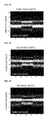
- FIG. 6 is an image of reflected light of a single layer thin film specimen obtained by an imaging spectrometer.
- FIG. 7 is an image of an interference fringe of a single layer thin film specimen obtained by an imaging spectrometer.
- FIG. 8 is a spectrum of a supercontinuum white light source.
- FIG. 9 is a graph illustrating a sensitivity characteristic of a CCD at every wavelength.
- FIG. 10 is an image of an interference fringe when a tungsten halogen lamp is used as a light source.
- FIG. 11 is an interference fringe image when a supercontinuum white light source is used as a light source.
- FIG. 12 is a view illustrating a process of calculating thickness and surface profile information of a multilayered film structure according to an exemplary embodiment of the present disclosure.
- FIG. 13 is a graph of an absolute reflectance measured in a reflected light measuring mode.
- FIG. 14 is a graph of a phase extracted by a phase shift algorithm in an interference mode.
- FIG. 15 is a cross-sectional view schematically illustrating reflection and transmission of light in a multilayered thin film.
- FIGS. 16 to 18 are a structure of a measuring sample in a simulation experiment of the present disclosure.
- FIG. 19 is a graph of an initial phase shift amount and an actual phase shift amount according to the number of phase shifts.
- FIGS. 20 to 26 are interference signals of an imaging spectrometer according to the number of phase shifts obtained by the simulation experiment of the present disclosure.
- FIG. 27 is a maximum phase shift error amount according to a wavelength obtained by the simulation experiment of the present disclosure.
- FIGS. 28 and 29 are comparison graphs of a phase shift amount obtained by an A-bucket and an error amount with respect to an actual phase shift amount.
- FIG. 30 is a non-linear phase by a thin film thickness.
- FIG. 31 is a graph of a thickness distribution obtained by an optimization algorithm.
- FIG. 32 is a measurement error of an IZTO thin film layer.
- FIG. 33 is a graph of a measurement error of a ZTO thin film layer.
- FIG. 34 is a graph of a non-linear phase and reflectance by a thickness of a thin film.
- FIG. 35 is a graph of a thickness distribution obtained by an optimization algorithm.
- FIG. 36 is a measurement error of an IZTO thin film layer.
- FIG. 37 is a graph of a measurement error of a ZTO thin film layer.
- FIG. 38 is a graph of a measurement error of an IZTO thin film layer when only a phase value is used to measure the thin film thickness and when both the phase value and the reflectance are applied.
- FIG. 39 is a graph of a measurement error of an IZTO thin film layer when only a phase value is used to measure the thin film thickness and when both the phase value and the reflectance are applied.
- Object to be measured 2 Beam splitter 3: Condensing lens 4: Detector 5: First condensing lens 6: Second condensing lens 10: Illumination optical module 11: Light source 12: Illumination optical system 20: First beam splitter 30: Interferometer module 31: Housing 32: First lens 33: Second beam splitter 34: Reference mirror 35: Blocking plate 36: Piezoelectric actuator 40: Imaging spectrometer module 41: Second lens 42: Slit 43: Diffractive optical element 44: CCD
- FIG. 4 illustrates a diagram of a measuring apparatus 100 of a thickness and a surface profile of a multilayered film structure using reflected light and interference light according to an exemplary embodiment of the present disclosure in a reflected light measuring mode.
- FIG. 5 illustrates a diagram of a measuring apparatus 100 of a thickness and a surface profile of a multilayered film structure using reflected light and interference light according to an exemplary embodiment of the present disclosure in an interference mode.
- the blocking plate 35 is driven by the plate driver to select a reflected light measuring mode and an interference mode.
- the measuring apparatus 100 of a thickness and a surface profile of a multilayered film structure using reflected light and interference light may be divided into an illumination optical module 10 which allows a beam from the light source 11 with a wide range of wavelengths to be incident onto an object to be measured, an interferometer module 30 which measures reflectance and a phase of the object to be measured, and an imaging spectrometer module 40 which obtains measurement light by a light intensity distribution at every wavelength.
- the light source 11 of the illumination optical module 10 may be configured by a tungsten-halogen lamp which emits white light and the white light may be emitted as collimating light with a constant width, by the optical system 12 .
- the white light which passes through the optical system 12 is incident onto the first beam splitter 20 .
- the first beam splitter 20 splits the incident white light at a ratio of 50:50 and the incident white light is not simultaneously split, but sequentially split in accordance with the measuring process.
- a reflection angle of the first beam splitter 20 is approximately 45 degrees with respect to the incident direction of the white light, so that the reflected white light is reflected to be perpendicular to the incident direction.
- the interferometer module 30 is located in accordance with the reflection angle of the first beam splitter 20 .
- the interferometer module 30 is configured to include a first lens 32 , a second beam splitter 33 , a reference mirror 34 , and a blocking plate 35 .
- the first lens 32 , the second beam splitter 33 , the reference mirror 34 , and the blocking plate 35 are mounted in a housing 31 .
- the interferometer module 30 is configured to include a transferring device which moves the housing 31 to the object to be measured.
- the white light reflected from the first beam splitter 20 is incident onto the object while passing through the first lens 32 .
- the second beam splitter 33 is located in front of a position where the white light which passes through the first lens 32 is incident onto the object, that is, in front of an in-focused position. In this case, a part of the light which reaches the second beam splitter 33 passes through the second beam splitter 33 to be irradiated onto the object to be measured. Further, in the reflected light measuring mode, the remaining light which is reflected from the second beam splitter 33 is absorbed by the blocking plate 35 to be removed.
- the blocking plate 35 is open, so that the light reflected from the second beam splitter 33 is reflected from the reference mirror 34 and also reflected from the second beam splitter 33 to be emitted.
- the interferometer module 30 is a system configured by the first lens 32 , the second beam splitter 33 , and the reference mirror 34 . Further, the blocking plate 35 is also included in the interferometer module 30 to selectively block the white light so that the interferometer module 30 operates in two modes.
- the white light which is split by the second beam splitter 33 to be incident onto the reference mirror 34 and the object to be measured is specifically irradiated onto the object to be measured to undergo changes in an amplitude and a phase. Since the changes in the amplitude and the phase are caused due to surface profile information and thickness information, the information may be separately measured according to the modes depending on whether the blocking plate 35 operates.
- the white light irradiated as described above is reflected again to pass through the second beam splitter 33 and then pass through the first lens 32 so that a traveling width of the white light is adjusted again and the white light becomes collimating light. Further, the white light passes through the first beam splitter and the second lens 41 to be incident onto the imaging spectrometer module 40 .
- the imaging spectrometer module 40 is an imaging spectrometer configured by a slit 42 , a diffractive optical element 43 , and a CCD 44 which obtains an interference fringe due to an optical path difference and the module obtains an interference signal having thickness information and surface profile information of a thin film.
- the white light split by the second beam splitter 33 is incident onto the object to be measured covered with a multilayered thin film and reflected from an upper layer of the thin film and a lower layer of the thin film and interfered with each other to obtain first reflected light.
- the blocking plate 35 is turned on to obtain a phase of the first reflected light so that only the thickness information of the thin film may be obtained.
- the blocking plate 35 is turned off to interfere the first reflected light which is reflected from the object to be measured with second reflected light from the reference mirror 34 , from the white light split by the second beam splitter 33 to obtain interference light.
- the surface profile information of the thin film may be obtained. That is, the surface information of the thin film including the thickness information of the thin film is obtained from the phase of the interference light so that the thickness information of the thin film and the surface information of the thin film are obtained from the surface information of the thin film in which thin film thickness information obtained from the first reflected light and thickness information of the thin film obtained from the interference light are included.
- the first beam splitter 20 is applied to the white light emitted from the light source 11 to be split into two light paths and one of two split white light paths is incident onto the object to be measured covered with the thin film and then first reflected light is obtained by interfering light reflected from the upper layer of the thin film and the lower layer of the thin film with each other. Further, the remaining one white light of two split white light paths is incident onto the reference mirror 34 and then reflected to obtain second reflected light. Here, the first reflected light and the second reflected light are combined to generate interference light.
- the transferring device which transfers the interferometer module 30 is included. Therefore, the phase is shifted by the transferring device and the reflected light and the interference light are obtained at every shifted phase so that the thickness and the surface profile of the thin film may be more precisely measured.
- the above-described transferring device is configured by a piezoelectric actuator 36 (PZT) and the piezoelectric actuator 36 scans along an optical axis direction to obtain an interference fringe due to the optical path difference by the imaging spectrometer.
- a precision transferring mechanism is required to transfer the interferometer module 30 by the piezoelectric actuator 36 .
- the piezoelectric actuator 36 may transfer the interferometer module 30 at a nanometer resolution using a position detecting sensor.
- a position detector an electrostatic type or a linear variable differential transformer (LVDT) is widely used.
- FIG. 6 is an image of reflected light of a single layer thin film specimen obtained by an imaging spectrometer
- FIG. 7 is an image of an interference fringe of a single layer thin film specimen obtained by an imaging spectrometer.
- the light used as a light source of FIGS. 6 and 7 is tungsten-halogen lamp. Since a spectral distribution of the light source has a Gaussian wavelength distribution approximately from 400 nm to 700 nm, according to a light intensity distribution at every wavelength obtained by the currently used image spectrometer, a spectroscopic image may be obtained only in a partial area (a center part).
- a light source having a wider broadband distribution may be preferably used. This is because the wider the wavelength band, the more the information (reflectance and phase information at every wavelength) on the specimen to be measured may be obtained. Accordingly, a supercontinuum white light source with a wavelength distribution of 450 nm to 2400 nm is used to broaden the wavelength band.
- FIG. 8 illustrates a spectrum of a supercontinuum white light source.
- the wavelength distribution is broad over an almost entire band from a visible ray band to an infrared ray region.
- a responsible band of the detector is restrictive, a limit of a wavelength band which may be actually obtained may be determined by the detector.
- the detector which is used for the experiment of the present disclosure is a CCD and the wavelength distribution band is illustrated in FIG. 9 .
- FIG. 10 illustrates an image of an interference fringe when a tungsten halogen lamp light source is used
- FIG. 11 illustrates an image of an interference fringe when a supercontinuum white light source is used. It is understood that, as illustrated in FIGS. 10 and 11 , an interference fringe over a wavelength band broader than that when the tungsten-halogen lamp is used as a light source may be obtained, as a result of obtaining an interference fringe at every wavelength through the experiment of the present disclosure.
- FIG. 12 is a view illustrating a process of calculating thickness and surface profile information of a multilayered film structure according to an exemplary embodiment of the present disclosure.
- a reflected light measuring method and a split white light measuring principle are combined to simultaneously measure the thickness and the surface profile of the thin film. Therefore, as illustrated in FIG. 12 , the thickness and the surface profile of a complex structure may be independently measured.
- An algorithm which is used to measure the thickness and the surface profile of the multilayered thin film structure uses a method for obtaining an absolute reflectance value of a measurement specimen using a reflected light measuring method and extracting a phase from an interference signal with a reference mirror using a phase shift algorithm.
- FIG. 13 illustrates a graph of an absolute reflectance measured in a reflected light measuring mode.
- FIG. 14 illustrates a graph of a phase extracted by a phase shift algorithm in an interference mode.
- the interference with the reference mirror is blocked by the blocking plate (a reflected light measuring mode) to obtain an absolute reflectance value of the object to be measured. Further, as illustrated in FIG. 14 , the blocking plate is open to obtain a phase component at every wavelength by means of the interference with the reference mirror.
- the obtained phase component is mainly divided into a linear component and a non-linear component as illustrated in FIG. 14 .
- a component by the thin film thickness is a non-linear component
- a function for a thin film thickness may be configured as represented in Equation 1, using the absolute reflectance and the non-linear phase component of the object to be measured (specimen).
- R E (k i ) is an absolute reflectance value for every wavenumber obtained by the experiment and R T (d j k i ) is a theoretical absolute reflectance value for every wavenumber by a thin film thickness d.
- ⁇ non-linear E (k i ) non-linear is a non-linear phase component value for every wavenumber obtained by the experiment and ⁇ non-linear T (d j k i ) is a theoretical phase component value for every wavenumber by a thin film thickness d.
- ⁇ refers to a weight by the absolute reflectance value and ⁇ is a weight by the non-linear phase component value. That is, since convergence of the function for the thin film thickness and accuracy of the thin film thickness d vary depending on the weights ⁇ and ⁇ , two values need to be adjusted in accordance with the situation.
- the phase signal by means of the interference with the reference mirror includes both the surface profile information and the thickness information of the thin film as represented in the following Equation 2, the surface profile information h is finally measured using the thin film thickness information d which is obtained from Equation 1.
- ⁇ (h,d j ,k i ) indicates all measured phase signals and ⁇ (d; k i ) is a theoretical phase signal by the thin film thickness. Therefore, when the thin film thickness information d is known, ⁇ (d; k i ) may be theoretically calculated.
- the phase signal by means of the interference with the reference mirror includes both the surface profile information and the thickness information of the thin film as represented in the following Equation 3, the surface profile information h is finally measured using the thin film thickness information d which is obtained from Equation 1.
- Equation 3 ⁇ E (k i ) is all measured phase component values and ⁇ T (d; k i ) is a theoretical phase component value which is mathematically calculated in advance using the thin film thickness information d obtained from Equation 1.
- the surface profile information h of the multilayered thin film may be improved through the above-described optimization process.
- the surface profile information h may be calculated by Equation 2.
- the thin film thickness information d is a value which includes all thickness information of the multilayered thin film.
- FIG. 15 illustrates a cross-sectional view schematically illustrating reflection and transmission of light in a multilayered thin film.
- incident light E i is incident onto each medium in the multilayered thin film structure, the light is repeatedly reflected and transmitted. Therefore, in the complex multilayered thin film structure, it is effective to represent the traveling of the incident light using a determinant.
- a distribution of the incident light E i on a j-th layer may be mainly classified into light traveling in a z-axis direction and light traveling in an opposite direction.
- the z-axis direction is represented by a positive sign (+) and the opposite direction is represented by a negative sign ( ⁇ )
- the distribution of light is represented by a matrix as represented in the following Equation 4.
- Equation 5 It is assumed that a relationship of Equation 5 is formed between two arbitrary positions z 1 and z 2 on a z-axis.
- Equation 6 S is defined as a characteristic matrix of the multiple thin film structure.
- the characteristic matrix is a function which determines a relationship in two arbitrary positions in a thin film and is configured by characteristic matrices on an interface and characteristic matrices of a j-th layer.
- the characteristic matrix on the interface is represented by the following Equation 7.
- Equation 7 indicates changes in an amplitude and a phase caused when the light is reflected or transmitted from the interface.
- the characteristic matrix on the j-th layer with a thickness d j is represented by the following Equation 12.
- N i and N j represent complex index of refraction of an incident medium and a transmissive medium, respectively, r ijp and r ijs are Fresnel reflection coefficients of a p wave and an s wave and t ijp and t ijs are Fresnel transmission coefficients of the p wave and the s wave.
- Equation 12 represents a phase change amount caused when light passes through the thin film layer.
- a characteristic matrix when the light travels from the i-th layer to the j-th layer is represented by multiplication of all I ij and L ij matrices between two layers.
- Equation 14 the reflection coefficient is defined as represented in Equation 15.
- Equation 16 ⁇ (d j k i ) represents a phase of the reflection coefficient of Equation 15
- a method which under an assumption that the reference phase change is an arbitrary phase regardless of a wavelength of a measuring light source, calculates the reference phase only using a light intensity measured at this time by a repetitive operation is applied to the measuring method according to the present disclosure to calculate a phase.
- a concept of an arbitrary phase measuring algorithm called A-bucket is as follows.
- I ij D j +V i cos( ⁇ i ⁇ 0) [Equation 17]
- Equation 19 A difference ⁇ ij between light intensities of Equation 17 and Equation 18 is defined by the following Equation 19.
- Equation 21 A conditional equation for calculating C i and S i which minimize the error function of Equation 20 is represented by the following Equation 21.
- Equation 21 is transformed into a matrix form to be represented by the following Equation 22.
- phase ⁇ i calculated from Equation 23 is calculated without any constraint on the reference phase, only information on the reference phase ⁇ j is required. Therefore, the reference phase value needs to be calculated in order to calculate C i and S i in Equation 23.
- Equation 24 the error function of ⁇ ij is defined by the least square method as represented in Equation 24.
- Equation 25 a conditional equation for calculating ⁇ j which minimizes the error function is represented by the following Equation 25.
- Equation 25 When Equation 25 is represented in the form of matrix, Equation 25 may be represented by the following Equation 26.
- Equation 26 cos ⁇ j and sin ⁇ j are calculated from Equation 26 and the reference phase ⁇ j is calculated therefrom as represented in the following Equation 27.
- Equation 21 is an equation for calculating C i and S i which minimize the error function E i of each measuring point from the reference phase ⁇ j and Equations 26 and 27 are equations for calculating ⁇ j which minimizes the error function E j when C i and S i are determined at all measuring points.
- step 1 the reference phase is assumed as an arbitrary value ⁇ j 0 .
- step 2 ⁇ j k is assigned to Equation 21 to calculate C i k and S i k which minimize the error function E i .
- step 3 C i k and S i k which are calculated in step 2 are assigned to Equations 25 and 26 to calculate ⁇ j k+1 which minimizes the error function E j .
- step 4 it is confirmed whether ⁇ j k+1 satisfies the condition of
- ⁇ j k+1 does not satisfy the condition, the number of repetition k is increased to repeat steps 2 and 3.
- c is a value which is very close to 0.
- step 5 after assigning ⁇ j k+1 to Equation 27 to calculate C i k and S i k which minimize the error function E i , the phase ⁇ i is calculated by Equation 23.
- the number of data to be measured which is required to perform the A-bucket algorithm is at least two and the number of phase shifts is at least four times.
- the thickness of an arbitrary thin film specimen is measured using a phase shifting method using the above-mentioned A-bucket algorithm and the reflected light measuring method, through a simulation experiment.
- FIGS. 16 to 18 illustrate a structure of a measuring sample in a simulation experiment of the present disclosure.
- a characteristic of the used light source is assumed that a Gaussian spectrum is distributed from 435 nm to 720 nm in consideration of the characteristic of the wavelength of the tungsten-halogen lamp which is mainly used.
- a sample to be measured is assumed that two transparent thin film (ZTO layer and IZTO layer) layers with different media are applied on a Cr base layer (substrate) as illustrated in FIGS. 16 to 18 .
- FIG. 19 illustrates a graph of an initial phase shift amount and an actual phase shift amount according to the number of phase shifts.
- ⁇ j 0 which is an existing phase shift value is assumed that a total of six phase shifts are performed at equal intervals of 50 nm
- the actual driven phase shift amount is driven at the various intervals of 33 nm, 97 nm, 92 nm, 170 nm, 230 nm, and 190 nm as illustrated in FIG. 19 .
- FIGS. 20 to 26 illustrate interference signals of an imaging spectrometer according to the number of phase shifts obtained by the simulation experiment of the present disclosure. That is, FIG. 20 is an interference signal obtained in the imaging spectrometer after one phase shift, FIG. 21 is an interference signal obtained in the imaging spectrometer after two phase shifts, FIG. 22 is an interference signal obtained in the imaging spectrometer after three phase shifts, FIG. 23 is an interference signal obtained in the imaging spectrometer after four phase shifts, FIG. 24 is an interference signal obtained in the imaging spectrometer after five phase shifts, FIG. 25 is an interference signal obtained in the imaging spectrometer after six phase shifts, and FIG. 25 is an interference signal obtained in the imaging spectrometer after seven phase shifts.
- the phase error amount is 1 nm or lower over the entire wavelength band of the used light source. Therefore, it is understood that the convergence is very high.
- FIGS. 28 and 29 illustrate comparison graphs of a phase shift amount obtained by an A-bucket and an error amount with respect to an actual phase shift amount. That is, when the analysis is performed based on the central wavelength of 570 nm of the light source, the phase shift amount obtained through the A-bucket with respect to the actual phase shift amount is illustrated in FIG. 28 and the error amount is illustrated in FIG. 29 .
- FIG. 30 illustrates a non-linear phase by a thickness of a thin film
- FIG. 31 illustrates a graph of a thickness distribution obtained by an optimization algorithm
- FIG. 32 illustrates a measurement error of an IZTO thin film layer
- FIG. 33 illustrates a graph of a measurement error of a ZTO thin film layer.
- the error value is approximately 1 nm or lower.
- FIG. 34 illustrates a graph of a non-linear phase and reflectance by a thickness of a thin film
- FIG. 35 illustrates a graph of a thickness distribution obtained by an optimization algorithm
- FIG. 36 illustrates a measurement error of an IZTO thin film layer
- FIG. 37 illustrates a graph of a measurement error of a ZTO thin film layer.
- FIG. 38 illustrates a graph of a measurement error of an IZTO thin film layer when only a phase value is used to measure the thickness of the thin film and when both the phase value and the reflectance are applied
- FIG. 39 illustrates a graph of a measurement error of an IZTO thin film layer when only a phase value is used to measure the thickness of the thin film and when both the phase value and the reflectance are applied.
- the present disclosure can be implemented as a computer-readable code in a computer-readable recording medium.
- the computer readable recording medium includes all types of recording devices in which data readable by a computer system is stored. Examples of the computer readable recording medium are ROM, RAM, CD-ROM, a magnetic tape, a floppy disk, an optical data storing device and also implemented as a carrier wave (for example, transmission through the Internet).
- the computer readable recording medium is distributed in computer systems connected through a network and a computer readable code is stored therein and executed in a distributed manner. Further, a functional program, a code, and a code segment which may implement the present disclosure may be easily deducted by the programmers in the art.
- the configuration and method of embodiments as described above may not be applied with limitation, but the embodiments may be configured by selectively combining all or a part of each embodiment such that various modifications may be made.
- the present disclosure relates to an apparatus for measuring a thickness and a surface profile of a multilayered film structure using an imaging spectral optical system and a measuring method.
Landscapes
- Physics & Mathematics (AREA)
- General Physics & Mathematics (AREA)
- Engineering & Computer Science (AREA)
- Mathematical Physics (AREA)
- Theoretical Computer Science (AREA)
- Data Mining & Analysis (AREA)
- Mathematical Optimization (AREA)
- Pure & Applied Mathematics (AREA)
- Mathematical Analysis (AREA)
- Computational Mathematics (AREA)
- Algebra (AREA)
- Databases & Information Systems (AREA)
- Software Systems (AREA)
- General Engineering & Computer Science (AREA)
- Computing Systems (AREA)
- Length Measuring Devices By Optical Means (AREA)
- Instruments For Measurement Of Length By Optical Means (AREA)
Abstract
Description
| Description of Main Reference Numerals of Drawings |
| 1: | Object to be measured | 2: | Beam splitter |
| 3: | Condensing lens | 4: | Detector |
| 5: | First condensing lens | 6: | Second condensing lens |
| 10: | Illumination optical module | 11: | Light source |
| 12: | Illumination optical system | 20: | First beam splitter |
| 30: | Interferometer module | 31: | Housing |
| 32: | First lens | 33: | Second beam splitter |
| 34: | Reference mirror | 35: | Blocking plate |
| 36: | Piezoelectric actuator | 40: | Imaging spectrometer module |
| 41: | Second lens | 42: | Slit |
| 43: | Diffractive optical element | 44: | CCD |
-
- 100: Measuring apparatus of thickness and surface profile of multilayered film structure using imaging spectral optical system
E(z 1)=SE(z)
β=2kNd cos [Equation 13]
I ij =D j +V i cos(Φi−0) [Equation 17]
I ij =D i +V i cos(Φj−0) [Equation 18]
Ψij =I ij −V i1 =C i(cos δj−1)+S i sin δj [Equation 19]
f=Σ i=1 n C i 2 ,g=Σ i=1 n C i S i ,h=Σ i=1 n S i 2
s i=Σi=1 n
Claims (15)
Applications Claiming Priority (3)
| Application Number | Priority Date | Filing Date | Title |
|---|---|---|---|
| KR1020160075238A KR101886919B1 (en) | 2016-06-16 | 2016-06-16 | Method for measuring threedimensional thickness profile of multi-layered film structure based on imaging spectrometer |
| KR10-2016-0075238 | 2016-06-16 | ||
| PCT/KR2016/009500 WO2017217590A1 (en) | 2016-06-16 | 2016-08-26 | Apparatus and method for measuring thickness and shape of multilayer film structure using image spectrometer |
Publications (2)
| Publication Number | Publication Date |
|---|---|
| US20190101373A1 US20190101373A1 (en) | 2019-04-04 |
| US10466031B2 true US10466031B2 (en) | 2019-11-05 |
Family
ID=60664152
Family Applications (1)
| Application Number | Title | Priority Date | Filing Date |
|---|---|---|---|
| US15/538,846 Active US10466031B2 (en) | 2016-06-16 | 2016-08-26 | Apparatus for measuring thickness and surface profile of multilayered film structure using imaging spectral optical system and measuring method |
Country Status (3)
| Country | Link |
|---|---|
| US (1) | US10466031B2 (en) |
| KR (1) | KR101886919B1 (en) |
| WO (1) | WO2017217590A1 (en) |
Families Citing this family (17)
| Publication number | Priority date | Publication date | Assignee | Title |
|---|---|---|---|---|
| KR101937043B1 (en) * | 2017-08-07 | 2019-01-14 | 한국표준과학연구원 | An apparatus and method for measuring the thickness and refractive index of multilayer thin films using angle-resolved spectroscopic reflectometry |
| KR102015216B1 (en) * | 2018-03-12 | 2019-08-28 | 한국표준과학연구원 | An apparatus and method for measuring the thickness and refractive index of multilayer thin films using angle-resolved spectral interference image according to polarization |
| JP6956673B2 (en) * | 2018-04-09 | 2021-11-02 | 三菱電機株式会社 | Film thickness measuring device |
| KR102202789B1 (en) | 2018-05-24 | 2021-01-14 | 주식회사 엘지화학 | Non-destructive thickness measurement method of reinforcing membranes for polymer electrolyte fuel cell having three layer |
| JP7210367B2 (en) * | 2019-04-23 | 2023-01-23 | 株式会社ディスコ | Thickness measuring device and processing device equipped with thickness measuring device |
| WO2021020604A1 (en) * | 2019-07-29 | 2021-02-04 | 한국표준과학연구원 | Measurement apparatus and measurement method for thickness and refractive index of multi-layer thin film, using angle-resolved spectral interference image according to polarization |
| JP7358185B2 (en) | 2019-10-15 | 2023-10-10 | 株式会社ディスコ | Thickness measurement device and processing equipment equipped with thickness measurement device |
| KR102391066B1 (en) * | 2020-02-25 | 2022-04-28 | 한국표준과학연구원 | Vibration insensitive interferometry for multilayer thin-film thickness profile measurement |
| KR102494082B1 (en) | 2021-01-28 | 2023-01-31 | 서울대학교산학협력단 | Measuring apparatus for thickness and profile for thin film using interference and wavenumber high frequency modulation, and measuring method using thereof |
| KR102570084B1 (en) | 2021-06-28 | 2023-08-24 | 서울대학교산학협력단 | The thickness measurement method using a three-dimensional reflectance surface |
| CN114993191A (en) * | 2022-04-28 | 2022-09-02 | 华东师范大学 | A device and method for obtaining dynamic image of liquid film thickness distribution |
| WO2024005484A1 (en) * | 2022-06-27 | 2024-01-04 | (주)오로스테크놀로지 | Multi-mode shape measurement device, and multi-mode shape measurement method using same |
| CN116734750B (en) * | 2023-08-15 | 2023-10-27 | 山西锦烁生物医药科技有限公司 | Intelligent detection method and system for thickness of ice layer of ice rink based on optical fiber sensor |
| CN117664917A (en) * | 2023-11-06 | 2024-03-08 | 华中科技大学 | A method and equipment for obtaining the complex refractive index distribution morphology of thin films |
| US12270982B1 (en) | 2023-11-06 | 2025-04-08 | Huazhong University Of Science And Technology | Method, device and computer-readable storage medium for obtaining complex refractive index distribution profile of film |
| CN118552646B (en) * | 2024-07-29 | 2024-10-18 | 季华实验室 | N-step phase shift fringe pattern generation method, device, equipment and storage medium |
| CN119245541B (en) * | 2024-09-18 | 2026-02-10 | 广州理工学院 | Methods, apparatus, equipment, and storage media for detecting the profile of the back surface of an optical lens. |
Citations (13)
| Publication number | Priority date | Publication date | Assignee | Title |
|---|---|---|---|---|
| US5042949A (en) * | 1989-03-17 | 1991-08-27 | Greenberg Jeffrey S | Optical profiler for films and substrates |
| US5129724A (en) * | 1991-01-29 | 1992-07-14 | Wyko Corporation | Apparatus and method for simultaneous measurement of film thickness and surface height variation for film-substrate sample |
| US5555471A (en) * | 1995-05-24 | 1996-09-10 | Wyko Corporation | Method for measuring thin-film thickness and step height on the surface of thin-film/substrate test samples by phase-shifting interferometry |
| JP2001311609A (en) * | 2000-04-28 | 2001-11-09 | Dainippon Screen Mfg Co Ltd | Method and apparatus for measuring film thickness |
| JP2001356050A (en) * | 2000-06-14 | 2001-12-26 | Toray Ind Inc | Spectroscopic method and method for forming film |
| JP2003222616A (en) * | 2002-01-30 | 2003-08-08 | Seiko Instruments Inc | Thin film-evaluating apparatus due to beat light resonance |
| US20040085544A1 (en) * | 2002-09-09 | 2004-05-06 | De Groot Peter J. | Interferometry method for ellipsometry, reflectometry, and scatterometry measurements, including characterization of thin film structures |
| US20050073692A1 (en) * | 2003-03-06 | 2005-04-07 | De Groot Peter J. | Profiling complex surface structures using scanning interferometry |
| US20050088663A1 (en) * | 2003-10-27 | 2005-04-28 | De Groot Peter J. | Scanning interferometry for thin film thickness and surface measurements |
| KR100631060B1 (en) | 2004-11-10 | 2006-10-04 | 한국과학기술원 | Apparatus and method for measuring thickness and profile of transparent thin-film by white-light interferometry |
| KR20080111723A (en) * | 2007-06-19 | 2008-12-24 | 한국과학기술원 | Thin Film Thickness and Shape Measurement Method Using Distributed White Light Interferometry based on Reflected Photometry |
| US7483147B2 (en) * | 2004-11-10 | 2009-01-27 | Korea Advanced Institute Of Science And Technology (Kaist) | Apparatus and method for measuring thickness and profile of transparent thin film using white-light interferometer |
| US20170314914A1 (en) * | 2016-04-28 | 2017-11-02 | Scott A. Chalmers | Optical profilometer |
Family Cites Families (1)
| Publication number | Priority date | Publication date | Assignee | Title |
|---|---|---|---|---|
| US91903A (en) * | 1869-06-29 | Improvement in the construction of sheet-metal boilers |
-
2016
- 2016-06-16 KR KR1020160075238A patent/KR101886919B1/en active Active
- 2016-08-26 US US15/538,846 patent/US10466031B2/en active Active
- 2016-08-26 WO PCT/KR2016/009500 patent/WO2017217590A1/en not_active Ceased
Patent Citations (13)
| Publication number | Priority date | Publication date | Assignee | Title |
|---|---|---|---|---|
| US5042949A (en) * | 1989-03-17 | 1991-08-27 | Greenberg Jeffrey S | Optical profiler for films and substrates |
| US5129724A (en) * | 1991-01-29 | 1992-07-14 | Wyko Corporation | Apparatus and method for simultaneous measurement of film thickness and surface height variation for film-substrate sample |
| US5555471A (en) * | 1995-05-24 | 1996-09-10 | Wyko Corporation | Method for measuring thin-film thickness and step height on the surface of thin-film/substrate test samples by phase-shifting interferometry |
| JP2001311609A (en) * | 2000-04-28 | 2001-11-09 | Dainippon Screen Mfg Co Ltd | Method and apparatus for measuring film thickness |
| JP2001356050A (en) * | 2000-06-14 | 2001-12-26 | Toray Ind Inc | Spectroscopic method and method for forming film |
| JP2003222616A (en) * | 2002-01-30 | 2003-08-08 | Seiko Instruments Inc | Thin film-evaluating apparatus due to beat light resonance |
| US20040085544A1 (en) * | 2002-09-09 | 2004-05-06 | De Groot Peter J. | Interferometry method for ellipsometry, reflectometry, and scatterometry measurements, including characterization of thin film structures |
| US20050073692A1 (en) * | 2003-03-06 | 2005-04-07 | De Groot Peter J. | Profiling complex surface structures using scanning interferometry |
| US20050088663A1 (en) * | 2003-10-27 | 2005-04-28 | De Groot Peter J. | Scanning interferometry for thin film thickness and surface measurements |
| KR100631060B1 (en) | 2004-11-10 | 2006-10-04 | 한국과학기술원 | Apparatus and method for measuring thickness and profile of transparent thin-film by white-light interferometry |
| US7483147B2 (en) * | 2004-11-10 | 2009-01-27 | Korea Advanced Institute Of Science And Technology (Kaist) | Apparatus and method for measuring thickness and profile of transparent thin film using white-light interferometer |
| KR20080111723A (en) * | 2007-06-19 | 2008-12-24 | 한국과학기술원 | Thin Film Thickness and Shape Measurement Method Using Distributed White Light Interferometry based on Reflected Photometry |
| US20170314914A1 (en) * | 2016-04-28 | 2017-11-02 | Scott A. Chalmers | Optical profilometer |
Non-Patent Citations (4)
| Title |
|---|
| Ghim, Young-Sik, Amit Suratkar, and Angela Davies. "Reflectometry-based wavelength scanning interferometry for thickness measurements of very thin wafers." Optics express18.7 (2010): 6522-6529. (Year: 2010). * |
| Ghim, Young-Sik, and Seung-Woo Kim. "Fast, precise, tomographic measurements of thin films." Applied Physics Letters 91.9 ( 2007): 091903. (Year: 2007). * |
| J.Schwider et al., "Dispersive interferometric profilometer," Optics Letters, vol. 19, No. 13, Jul. 1, 1994, pp. 995-998. |
| U. Schnell et al., "Dispersive white-light interferometry for absolute distance measurement with dielectric multilayer systems on the target," Optic Letters, vol. 21, No. 7, Apr. 1, 1996, pp. 528-530. |
Also Published As
| Publication number | Publication date |
|---|---|
| KR20170142240A (en) | 2017-12-28 |
| WO2017217590A1 (en) | 2017-12-21 |
| US20190101373A1 (en) | 2019-04-04 |
| KR101886919B1 (en) | 2018-09-11 |
Similar Documents
| Publication | Publication Date | Title |
|---|---|---|
| US10466031B2 (en) | Apparatus for measuring thickness and surface profile of multilayered film structure using imaging spectral optical system and measuring method | |
| US9377292B2 (en) | Interferometry employing refractive index dispersion broadening of interference signals | |
| CN110986818B (en) | Spectral beam profiling | |
| US8339617B2 (en) | Film thickness measuring device and film thickness measuring method | |
| KR100916618B1 (en) | Thin Film Thickness and Shape Measurement Method Using Distributed White Light Interferometry based on Reflected Photometry | |
| US7046361B1 (en) | Positioning two elements using an alignment target with a designed offset | |
| US11243070B2 (en) | Apparatus and method for multilayer thin film thickness measurement using single-shot angle-resolved spectral reflectometry | |
| US9927224B2 (en) | Thickness measuring apparatus and thickness measuring method | |
| JP6196119B2 (en) | Shape measuring apparatus and shape measuring method | |
| WO2013061417A1 (en) | Film thickness measurement method | |
| US20130077100A1 (en) | Surface shape measurement method and surface shape measurement apparatus | |
| KR102079588B1 (en) | Method measuring thickness and refractive index of planar samples based on fabry-perot interferometer | |
| KR20120034012A (en) | Temperature measuring method and storage medium | |
| WO2013099107A1 (en) | Method for measuring film thickness distribution | |
| CN109813430B (en) | Fourier transform interferometer using metasurfaces | |
| US10132612B2 (en) | Method and assembly for determining the thickness of a layer in a sample stack | |
| US8081319B2 (en) | Adjustable two dimensional lamellar grating | |
| JPH09119812A (en) | Method and device for featuring multilayered film structure and measuring distance between two planes directly facing film thereof | |
| KR101722815B1 (en) | Measuring method of surface of specimen and measurement apparatus of surface of specimen | |
| KR100699317B1 (en) | Thickness and Shape Measurement System | |
| US11112234B2 (en) | Multi-probe gauge for slab characterization | |
| US11073372B2 (en) | Multi-probe gauge for slab characterization | |
| JP3864719B2 (en) | Film thickness measuring method and film thickness measuring apparatus | |
| CN110312909B (en) | Method and assembly for determining layer thickness in a sample stack | |
| KR100747044B1 (en) | Thickness and Shape Measurement System |
Legal Events
| Date | Code | Title | Description |
|---|---|---|---|
| AS | Assignment |
Owner name: KOREA RESEARCH INSTITUTE OF STANDARDS AND SCIENCE, Free format text: ASSIGNMENT OF ASSIGNORS INTEREST;ASSIGNORS:GHIM, YOUNG-SIK;RHEE, HYUG-GYO;LEE, YUN WOO;REEL/FRAME:043332/0845 Effective date: 20170719 |
|
| FEPP | Fee payment procedure |
Free format text: ENTITY STATUS SET TO SMALL (ORIGINAL EVENT CODE: SMAL); ENTITY STATUS OF PATENT OWNER: SMALL ENTITY |
|
| STPP | Information on status: patent application and granting procedure in general |
Free format text: NOTICE OF ALLOWANCE MAILED -- APPLICATION RECEIVED IN OFFICE OF PUBLICATIONS |
|
| STPP | Information on status: patent application and granting procedure in general |
Free format text: PUBLICATIONS -- ISSUE FEE PAYMENT VERIFIED |
|
| STCF | Information on status: patent grant |
Free format text: PATENTED CASE |
|
| MAFP | Maintenance fee payment |
Free format text: PAYMENT OF MAINTENANCE FEE, 4TH YR, SMALL ENTITY (ORIGINAL EVENT CODE: M2551); ENTITY STATUS OF PATENT OWNER: SMALL ENTITY Year of fee payment: 4 |