US10444282B2 - Test point insertion for low test pattern counts - Google Patents
Test point insertion for low test pattern counts Download PDFInfo
- Publication number
- US10444282B2 US10444282B2 US14/884,611 US201514884611A US10444282B2 US 10444282 B2 US10444282 B2 US 10444282B2 US 201514884611 A US201514884611 A US 201514884611A US 10444282 B2 US10444282 B2 US 10444282B2
- Authority
- US
- United States
- Prior art keywords
- conflicts
- conflict
- test
- internal signal
- faults
- Prior art date
- Legal status (The legal status is an assumption and is not a legal conclusion. Google has not performed a legal analysis and makes no representation as to the accuracy of the status listed.)
- Active
Links
- 238000012360 testing method Methods 0.000 title claims abstract description 129
- 238000003780 insertion Methods 0.000 title abstract description 44
- 230000037431 insertion Effects 0.000 title abstract description 44
- 238000000034 method Methods 0.000 claims abstract description 66
- 238000013461 design Methods 0.000 claims abstract description 35
- 238000012545 processing Methods 0.000 claims description 8
- 238000004458 analytical method Methods 0.000 claims description 3
- 230000005284 excitation Effects 0.000 claims description 3
- 238000005516 engineering process Methods 0.000 abstract description 26
- 230000008569 process Effects 0.000 description 10
- 230000008901 benefit Effects 0.000 description 6
- 238000004088 simulation Methods 0.000 description 5
- 230000000903 blocking effect Effects 0.000 description 4
- 230000001419 dependent effect Effects 0.000 description 3
- 238000001514 detection method Methods 0.000 description 3
- 230000006870 function Effects 0.000 description 3
- 230000007246 mechanism Effects 0.000 description 3
- 230000003287 optical effect Effects 0.000 description 3
- 230000002093 peripheral effect Effects 0.000 description 3
- 239000003795 chemical substances by application Substances 0.000 description 2
- 238000004891 communication Methods 0.000 description 2
- 238000002347 injection Methods 0.000 description 2
- 239000007924 injection Substances 0.000 description 2
- 230000001902 propagating effect Effects 0.000 description 2
- 241000321453 Paranthias colonus Species 0.000 description 1
- 238000013459 approach Methods 0.000 description 1
- 230000005540 biological transmission Effects 0.000 description 1
- 230000015572 biosynthetic process Effects 0.000 description 1
- 230000006835 compression Effects 0.000 description 1
- 238000007906 compression Methods 0.000 description 1
- 238000013500 data storage Methods 0.000 description 1
- 230000007547 defect Effects 0.000 description 1
- 238000003745 diagnosis Methods 0.000 description 1
- 238000010586 diagram Methods 0.000 description 1
- 230000000694 effects Effects 0.000 description 1
- 238000002546 full scan Methods 0.000 description 1
- 230000005055 memory storage Effects 0.000 description 1
- 238000005192 partition Methods 0.000 description 1
- 230000000644 propagated effect Effects 0.000 description 1
- 230000008707 rearrangement Effects 0.000 description 1
- 230000009467 reduction Effects 0.000 description 1
- 238000010187 selection method Methods 0.000 description 1
- 239000004065 semiconductor Substances 0.000 description 1
- 239000007787 solid Substances 0.000 description 1
- 239000000243 solution Substances 0.000 description 1
- 238000012916 structural analysis Methods 0.000 description 1
- 238000003786 synthesis reaction Methods 0.000 description 1
- 230000009897 systematic effect Effects 0.000 description 1
- 238000012546 transfer Methods 0.000 description 1
- 230000007704 transition Effects 0.000 description 1
Images


Classifications
-
- G—PHYSICS
- G01—MEASURING; TESTING
- G01R—MEASURING ELECTRIC VARIABLES; MEASURING MAGNETIC VARIABLES
- G01R31/00—Arrangements for testing electric properties; Arrangements for locating electric faults; Arrangements for electrical testing characterised by what is being tested not provided for elsewhere
- G01R31/28—Testing of electronic circuits, e.g. by signal tracer
- G01R31/317—Testing of digital circuits
- G01R31/3181—Functional testing
- G01R31/3183—Generation of test inputs, e.g. test vectors, patterns or sequences
- G01R31/318307—Generation of test inputs, e.g. test vectors, patterns or sequences computer-aided, e.g. automatic test program generator [ATPG], program translations, test program debugging
-
- G—PHYSICS
- G01—MEASURING; TESTING
- G01R—MEASURING ELECTRIC VARIABLES; MEASURING MAGNETIC VARIABLES
- G01R31/00—Arrangements for testing electric properties; Arrangements for locating electric faults; Arrangements for electrical testing characterised by what is being tested not provided for elsewhere
- G01R31/28—Testing of electronic circuits, e.g. by signal tracer
- G01R31/317—Testing of digital circuits
- G01R31/3181—Functional testing
- G01R31/3183—Generation of test inputs, e.g. test vectors, patterns or sequences
- G01R31/318371—Methodologies therefor, e.g. algorithms, procedures
-
- G—PHYSICS
- G01—MEASURING; TESTING
- G01R—MEASURING ELECTRIC VARIABLES; MEASURING MAGNETIC VARIABLES
- G01R31/00—Arrangements for testing electric properties; Arrangements for locating electric faults; Arrangements for electrical testing characterised by what is being tested not provided for elsewhere
- G01R31/28—Testing of electronic circuits, e.g. by signal tracer
- G01R31/317—Testing of digital circuits
- G01R31/3181—Functional testing
- G01R31/3183—Generation of test inputs, e.g. test vectors, patterns or sequences
- G01R31/318342—Generation of test inputs, e.g. test vectors, patterns or sequences by preliminary fault modelling, e.g. analysis, simulation
Definitions
- the presently disclosed techniques relates to the field of circuit testing technology.
- Various implementations of the disclosed techniques may be particularly useful for reducing test data by inserting test points.
- Contemporary electronic design automation (EDA) tools in general and automatic test pattern generation (ATPG) in particular are capable of producing tests that offer high coverage of failures occurring in large and complex semiconductor digital designs. Notwithstanding the success of test compression, ATPG-produced test sets continue to grow at alarming rates.
- test point insertion techniques attempt to improve the fault detection likelihood while minimizing a necessary hardware real estate. They select internal lines in a circuit to subsequently add control points or observation points in order to activate (excite) faults or observe them, respectively. Identification of potential test point candidates is a complex problem because of several interacting factors. In general, optimal test point insertion for circuits with reconvergent fan-outs is an NP-complete problem and, hence, numerous empirical guidelines and approximate techniques have been proposed to identify suitable test points (control points and observation points) locations and improve the overall circuit testability.
- test point Depending on how a test point is driven or observed, its insertion may require a few extra gates and wires routed to or from additional flip-flops to be included in scan chains. As it introduces area and performance penalty, the number of test points is usually limited. Furthermore, the identification of test points must be computationally inexpensive despite the structural complexity of large designs.
- a probabilistic fault simulation which computes the impact of a new control point in the presence of the control points already selected, is used as a vehicle to select test points.
- test point insertion techniques can improve the fault detection likelihood, but may not affect test pattern counts at all.
- Kumar, A., Rajski, J., Reddy, S. M., and Rinderknecht, T. “On the generation of compact deterministic test sets for BIST ready designs”, Proceedings of the IEEE Asian Test Symposium, ATS'13, 201-206, 2013, which is incorporated herein by reference, the reduction of these counts can average anywhere between 0 and 35%. Therefore, it is desirable to develop new test point insertion techniques that can reduce the volume of test data.
- Various aspects of the disclosed technology relate to conflict-reducing test point insertion techniques.
- a method executed by at least one processor of a computer, comprising: determining locations in a circuit design for inserting test points based on internal signal conflicts caused by detecting multiple faults with a single test pattern; inserting test points at the locations.
- a method executed by at least one processor of a computer, comprising: computing internal signal conflict metrics; adding/adjusting test points to/at locations selected based on internal signal conflict metrics; and repeating the computing and the adding/adjusting until one of one or more predetermined conditions is met.
- non-transitory computer-readable media storing computer-executable instructions for causing one or more processors to perform a method, wherein the method comprises: determining locations in a circuit design for inserting test points based on internal signal conflicts caused by detecting multiple faults with a single test pattern; inserting test points at the locations.
- non-transitory computer-readable media storing computer-executable instructions for causing one or more processors to perform a method, wherein the method comprises: adding/adjusting test points to/at locations selected based on internal signal conflict metrics; and repeating the computing and the adding/adjusting until one of one or more predetermined conditions is met.
- test points may be control points.
- the internal signal conflicts may comprise horizontal conflicts.
- the horizontal conflict of a branch of a net in the circuit design may be measured based on numbers of faults being blocked by setting the branch to a signal of “0” and of “1”, respectively.
- the internal signal conflicts may comprise vertical conflicts.
- the vertical conflict of a stem of a net may be measured based on numbers of conflicts due to fault propagation conditions and logic values being forward-implied by the conditions.
- FIG. 1 illustrates a programmable computer system with which various embodiments of the disclosed technology may be employed.
- FIG. 2 illustrates an example of a test point insertion tool according to various embodiments of the disclosed technology.
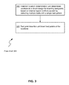
- FIG. 3 illustrates a flowchart 300 showing a process of test point insertion that may be implemented according to various examples of the disclosed technology.
- FIG. 4 illustrates an example of internal signal conflicts.
- FIG. 5 illustrates an example of a circuit for explaining fault blocking mechanisms.
- FIG. 6 illustrates another example of a circuit for explaining fault blocking mechanisms.
- FIG. 7 illustrates an example of horizontal conflicts.
- FIG. 8 illustrates another flowchart showing a process of test point insertion that may be implemented according to various examples of the disclosed technology.
- FIG. 9 illustrates an example of vertical conflicts.
- Some of the techniques described herein can be implemented in software instructions stored on a computer-readable medium, software instructions executed on a computer, or some combination of both. Some of the disclosed techniques, for example, can be implemented as part of an electronic design automation (EDA) tool. Such methods can be executed on a single computer or on networked computers.
- EDA electronic design automation
- the term “design” is intended to encompass data describing an entire integrated circuit device. This term also is intended to encompass a smaller group of data describing one or more components of an entire device, however, such as a portion of an integrated circuit device. Still further, the term “design” also is intended to encompass data describing more than one microdevice, such as data to be used to form multiple microdevices on a single wafer.
- FIG. 1 shows an illustrative example of a computing device 101 .
- the computing device 101 includes a computing unit 103 with a processing unit 105 and a system memory 107 .
- the processing unit 105 may be any type of programmable electronic device for executing software instructions, but will conventionally be a microprocessor.
- the system memory 107 may include both a read-only memory (ROM) 109 and a random access memory (RAM) 111 .
- ROM read-only memory
- RAM random access memory
- both the read-only memory (ROM) 109 and the random access memory (RAM) 111 may store software instructions for execution by the processing unit 105 .
- the processing unit 105 and the system memory 107 are connected, either directly or indirectly, through a bus 113 or alternate communication structure, to one or more peripheral devices.
- the processing unit 105 or the system memory 107 may be directly or indirectly connected to one or more additional memory storage devices, such as a “hard” magnetic disk drive 115 , a removable magnetic disk drive 117 , an optical disk drive 119 , or a flash memory card 121 .
- the processing unit 105 and the system memory 107 also may be directly or indirectly connected to one or more input devices 123 and one or more output devices 125 .
- the input devices 123 may include, for example, a keyboard, a pointing device (such as a mouse, touchpad, stylus, trackball, or joystick), a scanner, a camera, and a microphone.
- the output devices 125 may include, for example, a monitor display, a printer and speakers.
- one or more of the peripheral devices 115 - 125 may be internally housed with the computing unit 103 .
- one or more of the peripheral devices 115 - 125 may be external to the housing for the computing unit 103 and connected to the bus 113 through, for example, a Universal Serial Bus (USB) connection.
- USB Universal Serial Bus
- the computing unit 103 may be directly or indirectly connected to one or more network interfaces 127 for communicating with other devices making up a network.
- the network interface 127 translates data and control signals from the computing unit 103 into network messages according to one or more communication protocols, such as the transmission control protocol (TCP) and the Internet protocol (IP).
- TCP transmission control protocol
- IP Internet protocol
- the interface 127 may employ any suitable connection agent (or combination of agents) for connecting to a network, including, for example, a wireless transceiver, a modem, or an Ethernet connection.
- TCP transmission control protocol
- IP Internet protocol
- connection agent or combination of agents
- the computer 101 is illustrated as an example only, and it not intended to be limiting.
- Various embodiments of the disclosed technology may be implemented using one or more computing devices that include the components of the computer 101 illustrated in FIG. 1 , which include only a subset of the components illustrated in FIG. 1 , or which include an alternate combination of components, including components that are not shown in FIG. 1 .
- various embodiments of the disclosed technology may be implemented using a multi-processor computer, a plurality of single and/or multiprocessor computers arranged into a network, or some combination of both.
- FIG. 2 illustrates an example of a test point insertion tool according to various embodiments of the disclosed technology.
- the test point insertion tool 200 includes two units: an insertion location determination unit 220 and a test point insertion unit 240 .
- Some implementations of the diagnosis tool 200 may cooperate with (or incorporate) one or both of an input database 205 and an output database 285 .
- the insertion location determination unit 220 determines locations in a circuit design for inserting test points based on internal signal conflicts.
- the test point insertion unit 240 then inserts test points at the determined locations.
- various examples of the disclosed technology may be implemented by a computing system, such as the computing system illustrated in FIG. 1 .
- one or both of the insertion location determination unit 220 and the test point insertion unit 240 may be implemented by executing programming instructions on one or more processors in a computing system such as the computing system illustrated in FIG. 1 .
- some other embodiments of the disclosed technology may be implemented by software instructions, stored on a non-transitory computer-readable medium, for instructing one or more programmable computers/computer systems to perform the functions of one or both of the insertion location determination unit 220 and the test point insertion unit 240 .
- non-transitory computer-readable medium refers to computer-readable medium that are capable of storing data for future retrieval, and not propagating electro-magnetic waves.
- the non-transitory computer-readable medium may be, for example, a magnetic storage device, an optical storage device, a “punched” surface type device, or a solid state storage device.
- insertion location determination unit 220 and the test point insertion unit 240 are shown as separate units in FIG. 2 , a single computer (or a single processor within a master computer) may be used to implement both of these units at different times, or components of these units at different times.
- the input database 205 and the output database 285 may be implemented using any suitable computer readable storage device. That is, either of the input database 205 and the output database 285 may be implemented using any combination of computer readable storage devices including, for example, microcircuit memory devices such as read-write memory (RAM), read-only memory (ROM), electronically erasable and programmable read-only memory (EEPROM) or flash memory microcircuit devices, CD-ROM disks, digital video disks (DVD), or other optical storage devices.
- the computer readable storage devices may also include magnetic cassettes, magnetic tapes, magnetic disks or other magnetic storage devices, punched media, holographic storage devices, or any other non-transitory storage medium that can be used to store desired information. While the input database 205 and the output database 285 are shown as separate units in FIG. 2 , a single data storage medium may be used to implement some or all of these databases.
- FIG. 3 illustrates a flowchart 300 showing a process of test point insertion that may be implemented according to various examples of the disclosed technology.
- FIG. 8 illustrates another flowchart 800 showing a process of test point insertion that may be implemented according to various examples of the disclosed technology.
- methods of test point insertion that may be employed according to various embodiments of the disclosed technology will be described with reference to the test point insertion tool 200 illustrated in FIG. 2 and the flow charts 300 and 800 in FIGS. 3 and 8 , respectively.
- alternate implementations of a test point insertion tool may be used to perform the methods of test point insertion in the flow chart 300 / 800 according to various embodiments of the disclosed technology.
- implementations of the test point insertion tool 200 may be employed to implement methods of test point insertion according to different embodiments of the disclosed technology other than the ones illustrated by the flow charts 300 and 800 .
- the insertion location determination unit 220 determines locations in a circuit design for inserting test points based on internal signal conflicts caused by detecting multiple faults with a single test pattern.
- the test point insertion unit 240 inserts test points at the determined locations.
- FIG. 4 illustrates an example of an internal signal conflict.
- input s 1 ( 460 ) of the AND gate 420 must be set to 1.
- input s 2 ( 470 ) of an OR gate 440 must assume the value of 0.
- stem s 0 ( 450 ) because of mutually opposed fault propagation requirements that correspond to different non-controlling values for gates driven by a common stem.
- a control point is placed on one of the stem branches.
- a 1-injection circuit such as an OR gate on branch s 1 ( 460 ), allowing 1-controllability of this line (an OR control point).
- a 0-injection circuit such as an AND gate can be placed on branch s 2 ( 470 ), allowing 0-controllability of this particular net (an AND control point).
- the internal signal conflicts may manifest themselves in a variety of ways.
- the internal signal conflicts comprise horizontal conflicts. Before defining the horizontal conflicts, several related concepts employed to assess a fault-blocking mechanism will be explained first.
- the number of faults whose propagation is blocked is determined based on the results of forward value propagation. Having set a given internal line to a logic value v, this value propagates subsequently forward as long as the outputs of gates visited along propagation paths can be uniquely determined. In particular, it applies to scenarios where v remains a controlling value for a visited gate G, or all inputs of G assume a non-controlling value. In FIG. 5 , for example, if one sets stem s 0 ( 505 ) to 1, then it causes the output of gates 530 , 550 and 560 to assume the value of 0.
- Every AND, NAND, OR, and NOR gate is said to block faults if the controlling value reaches its input(s). For instance, faults C 2 and C 4 are blocked due to 1 at input s 2 ( 535 ). Also, faults affecting input 525 of gate 560 will be blocked, as their only propagation path leads to the output of gate 560 . Finally, 0 at input s 1 ( 535 ) of gate 510 blocks its second input 527 and, thus, any fault observed on the output of C 1 cannot move further towards a circuit output. The same applies to faults propagating through C 3 .
- Fan-out-free regions i.e., treelike gate structures.
- cones presented in figures herein are fan-out-free regions.
- all faults within that fan-out-free region are unable to propagate to the output (e.g., faults C 1 and C 3 in FIG. 5 ).
- fault propagation conditions depend on a combined status of all of its output branches.
- FIG. 4 The main concept of a horizontal conflict is illustrated in FIG. 4 .
- a logic value of 1 is necessary to propagate faults through the AND gate 420 , whereas a logic value of 0 is needed to achieve the same with the OR gate 440 .
- stem s 0 ( 450 ) is set to 0, then faults C 1 ( 410 ) are blocked.
- stem s 0 ( 450 ) blocks faults C 2 ( 420 ).
- u s and U s are quantities of faults blocked by setting stem s to 0 and 1, respectively.
- the degree of horizontal conflicts is measured as a minimal number of blocked faults. It relates to a lower bound of conflicts at a given stem or, stated differently, it indicates the amount of faults whose blocking is inevitable.
- H s min ⁇ u s
- U s ⁇ min ⁇ D C1
- FIG. 7 illustrates a slightly more complicated case of horizontal conflicts.
- a stem 710 features three output branches 720 , 730 and 740 .
- Cones C 1 ( 750 ), C 2 ( 760 ), and C 3 ( 770 ) drive the corresponding gates 755 . 765 and 775 , respectively.
- control points may be inserted on some branches.
- an OR gate may be inserted on the branch 730 and an AND gate may be inserted on the branch 740 .
- test points The number of test points is usually limited as the test point insertion introduces area and performance penalty.
- One solution is to use a threshold denoted as ⁇ for blocked faults. Only branches that have the number of blocked faults above the threshold ⁇ are considered for the test point insertion.
- the threshold ⁇ may be user-defined and circuit-specific.
- the flow chart 800 is used here to illustrate how test points are inserted to reduce horizontal conflicts according to some embodiments of the disclosed technology.
- the insertion location determination unit 220 computes internal signal conflict metrics such as those for horizontal conflict metrics.
- the test point insertion unit 240 adds/adjusts test points on locations selected based on the internal signal conflict metrics. For example, appropriate test points are added to branches having the number of blocked faults above ⁇ . Or branches having the first n (n>0) largest blocked faults. If none of one or more predetermined termination conditions is met, internal signal conflict metrics are recomputed on the design with the added test points and the process repeats. When the operation 820 is repeated, some of the existing test points may be replaced with new test points.
- H s Another threshold for H s (denoted as ⁇ ) may be introduced to reduce the computation time. Only branches on a stem with H s > ⁇ may be considered for the test point insertion. When the operation 810 is repeated, H s is also recomputed. One example of a predetermined termination condition is all eligible branches are examined.
- test points already in may visibly impact further test point insertion decisions.
- FIG. 9 illustrates an example of vertical conflicts. If a gate 2 is set to 0 to enable propagation of faults C 3 ( 930 ), then at least one of its inputs 922 and 927 needs to be set to 0. This precludes propagation of faults C 1 ( 910 ), faults C 2 ( 920 ), or both. Propagation of faults C 4 ( 940 ) is also not possible. On the other hand, having 1 on the output ( 925 ) of the gate 2 (as a result of attempts to propagate faults C 1 ( 910 ) and faults C 2 ( 920 )) blocks faults C 3 ( 930 ). As can be seen, a “vertical” conflict occurs at the stem between logic values being forward-implied and those resulting from backward justifications that are needed to propagate different groups of faults.
- B x1 0 (this value would block any fault propagation).
- b x (B x ) for line x equals the number of blocked faults when x is set to 1 (0).
- the vertical conflict analysis may also involve information regarding the numbers f x and F x of 0s and 1s occurring at a given line x as a result of the justification of other gates.
- F xk As an example, consider computation of and F x1 for the gate 4 in FIG. 9 .
- the number of 0s reaching its input x 1 ( 947 ), f x1 is equal to the number of forward implied 0s on stem x 0 ( 925 ), f x0 , plus the number b x2 of 0s required at input x 2 ( 949 ) of the gate 5 to propagate faults C 4 ( 940 ).
- b x2 0 since 0 is a controlling value for an AND gate.
- f x1 f x0 .
- the number of 1s (F x1 ) equals the number of 1s at x 0 ( 925 ), F x0 , plus 1s needed to propagate faults C 4 ( 940 ), B x2 .
- F x1 F x0 +B x2 .
- the value of F x0 may be defined as the minimum of the numbers of 1s at the inputs of the gate 2 .
- the number f x0 of 0s propagated through the gate 2 can be expressed as the maximum of the numbers of 0s at its inputs (f v2 and f w1 ).
- a value of f x0 is 0 because neither the gate 1 nor the gate 3 requires 0 to propagate faults C 1 or C 2 .
- f x0 and F x0 are obtained by structural analysis of a circuit net list in conjunction with its fault list to find faults that would otherwise be blocked, if 1 and 0 are applied, respectively, to a gate input.
- F s F k
- F s f k
- a measure of a vertical conflict at stem s may be derived.
- Eq. 9 estimates the amount of inconsistency between signals required due to fault propagation conditions and logic values being forward implied by such decisions. Inserting a test point at a stem can alleviate this type of conflicts.
- the process shown by the flow chart 800 may be employed to insert test points for reducing vertical conflicts.
- Horizontal and vertical conflicts may be analyzed and processed at the same time or in sequence.
Landscapes
- Engineering & Computer Science (AREA)
- General Engineering & Computer Science (AREA)
- Physics & Mathematics (AREA)
- General Physics & Mathematics (AREA)
- Computer Hardware Design (AREA)
- Tests Of Electronic Circuits (AREA)
Abstract
Description
H s=min{u s ,U s} (1)
b x0 =b x0 +b x2 + . . . +b xn (2)
B xo =B x1 +B x2 + . . . +B xn (3)
f xk =f x0 +Σb xi i≠k (4)
f s =f k f s =F k (5a)
F s =F k F s =f k (5b)
f s=max{f k } f s=min{F k} (6a)
F s=min{F k } F s=max{f k} (6b)
F s=min{f k } f s=max{F k} (7a)
F s=max{F k } F s=min{f k} (7b)
f s=(min{f a ,f b}+min{F a ,F b})/2
F s=(min{f a ,F b}+min{F a ,f b})/2 (8)
V s=max{min{b s ,F s}, min{B s ,f s} } (9)
Claims (24)
Priority Applications (1)
| Application Number | Priority Date | Filing Date | Title |
|---|---|---|---|
| US14/884,611 US10444282B2 (en) | 2014-10-16 | 2015-10-15 | Test point insertion for low test pattern counts |
Applications Claiming Priority (2)
| Application Number | Priority Date | Filing Date | Title |
|---|---|---|---|
| US201462064900P | 2014-10-16 | 2014-10-16 | |
| US14/884,611 US10444282B2 (en) | 2014-10-16 | 2015-10-15 | Test point insertion for low test pattern counts |
Publications (2)
| Publication Number | Publication Date |
|---|---|
| US20160109517A1 US20160109517A1 (en) | 2016-04-21 |
| US10444282B2 true US10444282B2 (en) | 2019-10-15 |
Family
ID=55748880
Family Applications (1)
| Application Number | Title | Priority Date | Filing Date |
|---|---|---|---|
| US14/884,611 Active US10444282B2 (en) | 2014-10-16 | 2015-10-15 | Test point insertion for low test pattern counts |
Country Status (1)
| Country | Link |
|---|---|
| US (1) | US10444282B2 (en) |
Cited By (1)
| Publication number | Priority date | Publication date | Assignee | Title |
|---|---|---|---|---|
| US12511462B1 (en) * | 2022-09-27 | 2025-12-30 | Cadence Design Systems, Inc. | Physical awareness of test-point sharing in a circuit design |
Families Citing this family (2)
| Publication number | Priority date | Publication date | Assignee | Title |
|---|---|---|---|---|
| US10361873B2 (en) | 2015-11-16 | 2019-07-23 | Mentor Graphics Corporation | Test point-enhanced hardware security |
| CN111880076B (en) * | 2020-07-14 | 2022-11-18 | 苏州浪潮智能科技有限公司 | Signal test point detection method, system and related assembly |
Citations (4)
| Publication number | Priority date | Publication date | Assignee | Title |
|---|---|---|---|---|
| US20020116690A1 (en) * | 2001-02-20 | 2002-08-22 | International Business Machines Corporation | Method for insertion of test points into integrated logic circuit designs |
| US7296249B2 (en) * | 2003-10-10 | 2007-11-13 | Thomas Hans Rinderknecht | Using constrained scan cells to test integrated circuits |
| US20100017760A1 (en) * | 2008-07-21 | 2010-01-21 | Synopsys, Inc. | Test design optimizer for configurable scan architectures |
| US20140101627A1 (en) * | 2012-10-05 | 2014-04-10 | Fujitsu Limited | Design assist apparatus, method for assisting design, and computer-readable recording medium having stored therein program for assisting design |
-
2015
- 2015-10-15 US US14/884,611 patent/US10444282B2/en active Active
Patent Citations (5)
| Publication number | Priority date | Publication date | Assignee | Title |
|---|---|---|---|---|
| US20020116690A1 (en) * | 2001-02-20 | 2002-08-22 | International Business Machines Corporation | Method for insertion of test points into integrated logic circuit designs |
| US20040098686A1 (en) * | 2001-02-20 | 2004-05-20 | Lackey David E. | Method for insertion of test points into integrated logic circuit designs |
| US7296249B2 (en) * | 2003-10-10 | 2007-11-13 | Thomas Hans Rinderknecht | Using constrained scan cells to test integrated circuits |
| US20100017760A1 (en) * | 2008-07-21 | 2010-01-21 | Synopsys, Inc. | Test design optimizer for configurable scan architectures |
| US20140101627A1 (en) * | 2012-10-05 | 2014-04-10 | Fujitsu Limited | Design assist apparatus, method for assisting design, and computer-readable recording medium having stored therein program for assisting design |
Non-Patent Citations (11)
| Title |
|---|
| Briers, A. J. and Totton, K. A. E., "Random Pattern Testability by Fault Simulation", Proceedings of the IEEE International Test Conference, ITC'86. 274-281, 1986. |
| Chang, S.-C., Chang, S.-S., Jone, W.-B., and Tsai, C.-C. 1998. A novel combinational testability analysis by considering signal correlation. In Proceedings of the IEEE International Test Conference. ITC'98. 658-667. |
| Cheng, K.-T., and Lin, C.-J., "Timing-Driven Test Point Insertion for Full-Scan and Partial-Scan BIST", Proceedings of the IEEE International Test Conference, ITC'95, 506-514, 1995. |
| Geuzebroek, M. J., van der Linden, J. T., and van de Goor, A. J. 2002. Test point insertion that facilitates ATPG in reducing test time and data volume. In Proceedings of the IEEE International Test Conference. ITC'02. 138-147. |
| Goldstein, L. H., and Thigpen, E. L. 1980. SCOAP: Sandia controllability/observability analysis program. In Proceedings of the IEEE Design Automation Conference. DAC'80. 190-196. |
| Isao et al. "Accelerated Test Points Selection Method for Scan-Based BIST" 1997, IEEE, pp. 359-364 (Year: 1997). * |
| Iyengar, V. S. and Brand, D., "Synthesis of Pseudorandom Pattern Testable Designs", Proceedings of the IEEE International Test Conference, ITC'89. 501-508, 1989. |
| Kumar, A., Rajski, J., Reddy, S.M., and Rinderknecht, T., "On the generation of compact deterministic test sets for BIST ready designs", Proceedings of the IEEE Asian Test Symposium, ATS'13, 201-206, 2013. |
| Nakao, M., Hatayama, K., and Highasi, I., "Accelerated test points selection method for scan-based BIST", Proceedings of the IEEE Asian Test Symposium, ATS'97, 359-364, 1997. |
| Seiss, B. H., Trouborst, P., and Schulz, M. 1991. Test point insertion for scan-based BIST. In Proceedings of the European Test Conference. ETC'91. 253-262. |
| Tamarapalli, N. and Rajski, J., "Constructive Multiphase Test Point Insertion for Scan-Based BIST", Proceedings of the IEEE International Test Conference, ITC'96. 649-658, 1996. |
Cited By (1)
| Publication number | Priority date | Publication date | Assignee | Title |
|---|---|---|---|---|
| US12511462B1 (en) * | 2022-09-27 | 2025-12-30 | Cadence Design Systems, Inc. | Physical awareness of test-point sharing in a circuit design |
Also Published As
| Publication number | Publication date |
|---|---|
| US20160109517A1 (en) | 2016-04-21 |
Similar Documents
| Publication | Publication Date | Title |
|---|---|---|
| US7131081B2 (en) | Scalable scan-path test point insertion technique | |
| US10775436B1 (en) | Streaming networks efficiency using data throttling | |
| Acero et al. | Embedded deterministic test points | |
| US10795751B2 (en) | Cell-aware diagnostic pattern generation for logic diagnosis | |
| US11585853B2 (en) | Trajectory-optimized test pattern generation for built-in self-test | |
| US10509072B2 (en) | Test application time reduction using capture-per-cycle test points | |
| US11408938B2 (en) | Bidirectional scan cells for single-path reversible scan chains | |
| WO2008041537A1 (en) | Generation device, generation method, program and recording medium | |
| US10444282B2 (en) | Test point insertion for low test pattern counts | |
| Konuk et al. | Design for low test pattern counts | |
| Kim et al. | SPAR: A new test-point insertion using shared points for area overhead reduction | |
| Lo et al. | Utilizing circuit structure for scan chain diagnosis | |
| US10078114B2 (en) | Test point circuit, scan flip-flop for sequential test, semiconductor device and design device | |
| Orailoglu | Microarchitectural synthesis for rapid BIST testing | |
| US10996273B2 (en) | Test generation using testability-based guidance | |
| US8468409B2 (en) | Speed-path debug using at-speed scan test patterns | |
| US20050235184A1 (en) | Semiconductor integrated circuit device and test method thereof | |
| US11010523B1 (en) | Prediction of test pattern counts for scan configuration determination | |
| US10796043B1 (en) | Non-adaptive pattern reordering to improve scan chain diagnostic resolution in circuit design and manufacture | |
| Yuan et al. | On systematic illegal state identification for pseudo-functional testing | |
| US9274171B1 (en) | Customer-transparent logic redundancy for improved yield | |
| US10234502B1 (en) | Circuit defect diagnosis based on sink cell fault models | |
| EP4305541B1 (en) | Test generation for structurally similar circuits | |
| Liao et al. | A parallel test pattern generation algorithm to meet multiple quality objectives | |
| Ko et al. | RTL scan design for skewed-load at-speed test under power constraints |
Legal Events
| Date | Code | Title | Description |
|---|---|---|---|
| AS | Assignment |
Owner name: MENTOR GRAPHICS CORPORATION, OREGON Free format text: ASSIGNMENT OF ASSIGNORS INTEREST;ASSIGNORS:RAJSKI, JANUSZ;MOGHADDAM, ELHAM K;MUKHERJEE, NILANJAN;AND OTHERS;SIGNING DATES FROM 20151001 TO 20151008;REEL/FRAME:036805/0245 |
|
| STPP | Information on status: patent application and granting procedure in general |
Free format text: DOCKETED NEW CASE - READY FOR EXAMINATION |
|
| STPP | Information on status: patent application and granting procedure in general |
Free format text: NON FINAL ACTION MAILED |
|
| STPP | Information on status: patent application and granting procedure in general |
Free format text: NOTICE OF ALLOWANCE MAILED -- APPLICATION RECEIVED IN OFFICE OF PUBLICATIONS |
|
| STPP | Information on status: patent application and granting procedure in general |
Free format text: PUBLICATIONS -- ISSUE FEE PAYMENT VERIFIED |
|
| STCF | Information on status: patent grant |
Free format text: PATENTED CASE |
|
| AS | Assignment |
Owner name: SIEMENS INDUSTRY SOFTWARE INC., TEXAS Free format text: MERGER AND CHANGE OF NAME;ASSIGNORS:MENTOR GRAPHICS CORPORATION;SIEMENS INDUSTRY SOFTWARE INC.;REEL/FRAME:056675/0285 Effective date: 20201230 |
|
| MAFP | Maintenance fee payment |
Free format text: PAYMENT OF MAINTENANCE FEE, 4TH YEAR, LARGE ENTITY (ORIGINAL EVENT CODE: M1551); ENTITY STATUS OF PATENT OWNER: LARGE ENTITY Year of fee payment: 4 |