US10439617B2 - Bidirectional gray code counter - Google Patents
Bidirectional gray code counter Download PDFInfo
- Publication number
- US10439617B2 US10439617B2 US15/146,483 US201615146483A US10439617B2 US 10439617 B2 US10439617 B2 US 10439617B2 US 201615146483 A US201615146483 A US 201615146483A US 10439617 B2 US10439617 B2 US 10439617B2
- Authority
- US
- United States
- Prior art keywords
- gray code
- code value
- logical
- bit
- significant bit
- Prior art date
- Legal status (The legal status is an assumption and is not a legal conclusion. Google has not performed a legal analysis and makes no representation as to the accuracy of the status listed.)
- Active, expires
Links
- 230000002457 bidirectional effect Effects 0.000 title claims abstract description 144
- 238000000034 method Methods 0.000 abstract description 9
- 238000013461 design Methods 0.000 abstract description 5
- ORQBXQOJMQIAOY-UHFFFAOYSA-N nobelium Chemical compound [No] ORQBXQOJMQIAOY-UHFFFAOYSA-N 0.000 description 57
- 230000001629 suppression Effects 0.000 description 43
- 230000004044 response Effects 0.000 description 14
- 238000004891 communication Methods 0.000 description 13
- 230000008901 benefit Effects 0.000 description 8
- 230000008859 change Effects 0.000 description 8
- 238000001514 detection method Methods 0.000 description 5
- 238000005265 energy consumption Methods 0.000 description 4
- 230000000630 rising effect Effects 0.000 description 4
- 238000012986 modification Methods 0.000 description 3
- 230000004048 modification Effects 0.000 description 3
- 230000001960 triggered effect Effects 0.000 description 3
- 238000006243 chemical reaction Methods 0.000 description 2
- 230000006870 function Effects 0.000 description 2
- 239000007787 solid Substances 0.000 description 2
- 230000005540 biological transmission Effects 0.000 description 1
- 230000001419 dependent effect Effects 0.000 description 1
- 238000004870 electrical engineering Methods 0.000 description 1
- 230000005670 electromagnetic radiation Effects 0.000 description 1
- 230000006872 improvement Effects 0.000 description 1
- 230000007774 longterm Effects 0.000 description 1
- 239000000463 material Substances 0.000 description 1
- 238000010295 mobile communication Methods 0.000 description 1
- 230000002265 prevention Effects 0.000 description 1
- 230000008569 process Effects 0.000 description 1
- 238000012545 processing Methods 0.000 description 1
- 238000012546 transfer Methods 0.000 description 1
- 230000001131 transforming effect Effects 0.000 description 1
- 230000007704 transition Effects 0.000 description 1
Images


Classifications
-
- H—ELECTRICITY
- H03—ELECTRONIC CIRCUITRY
- H03K—PULSE TECHNIQUE
- H03K23/00—Pulse counters comprising counting chains; Frequency dividers comprising counting chains
- H03K23/004—Counters counting in a non-natural counting order, e.g. random counters
- H03K23/005—Counters counting in a non-natural counting order, e.g. random counters using minimum change code, e.g. Gray Code
-
- H—ELECTRICITY
- H03—ELECTRONIC CIRCUITRY
- H03M—CODING; DECODING; CODE CONVERSION IN GENERAL
- H03M7/00—Conversion of a code where information is represented by a given sequence or number of digits to a code where the same, similar or subset of information is represented by a different sequence or number of digits
- H03M7/14—Conversion to or from non-weighted codes
- H03M7/16—Conversion to or from unit-distance codes, e.g. Gray code, reflected binary code
Definitions
- the present disclosure relates to the field of electronic circuits. More particularly, the present disclosure relates to a bidirectional Gray code counter.
- Legacy bidirectional counter circuitry focuses on providing bidirectional binary counters for simplicity and ease of design.
- the bidirectional binary counters present the disadvantages of high levels of energy consumption and lower possible counter frequencies due to multiple bits being changed by the counter on each increment or decrement.
- the bidirectional binary counters require greater physical area for components to implement the bidirectional binary counters.
- FIG. 1 illustrates an example bidirectional Gray code counter, according to various embodiments.
- FIG. 2 illustrates an example bidirectional Gray code counter with clock suppression circuitry, according to various embodiments.
- FIG. 3 illustrates an example bidirectional Gray code counter with update suppression circuitry, according to various embodiments.
- FIG. 4 illustrates an example bidirectional Gray code counter with wrap enablement.
- FIG. 5 illustrates an example bidirectional Gray code counter with a stepped bidirectional indicator signal.
- FIG. 6 illustrates an example computing device that may employ the apparatuses and/or methods described herein.
- a bidirectional Gray code counter may include a sequential logic element to store a Gray code value and logic circuitry.
- the logic circuitry may determine, based on a bidirectional indicator signal, whether to increment or decrement the Gray code value and update, through performance of an increment or a decrement of the Gray code value based on the determination of whether to increment or decrement the Gray code value, the Gray code value to be a sequential Gray code value and replace the Gray code value stored in the sequential logic element with the updated Gray code value.
- phrase “A and/or B” means (A), (B), or (A and B).
- phrase “A, B, and/or C” means (A), (B), (C), (A and B), (A and C), (B and C), or (A, B and C).
- circuitry may refer to, be part of, or include an Application Specific Integrated Circuit (ASIC), an electronic circuit, a processor (shared, dedicated, or group) and/or memory (shared, dedicated, or group) that execute one or more software or firmware programs, a combinational logic circuit, and/or other suitable components that provide the described functionality.
- ASIC Application Specific Integrated Circuit
- logical one and “high state” may refer to a high logical state, which may include a digital value of one, 5 volts, 2.3 volts, and/or any other value understood by one having ordinary skill in the art to constitute a logical one or logical high state in logic circuitry.
- logical zero and “low state” may refer to a low logical state, which may include a digital value of zero, 0 volts, ground, and/or any other value understood by one having ordinary skill in the art to constitute a logical zero or logical low state in logic circuitry.
- the operations and/or features associated with a “logical one” and/or “high state” may be transposed with the operations and/or features associated with a “logical zero” and/or “low state,” such that operations and/or features described throughout this disclosure being associated with a “logical one” and/or “high state” may be associated with a “logical zero” and/or “low state” in these embodiments, and vice versa.
- Gray code value and/or binary value may be represented as (g N-1 , g N-2 , g N-3 , . . . g 2 , g 1 , g 0 ), wherein N is equal to the number of bits within the Gray code value and/or binary value.
- g N-1 may be referred to as the most significant bit of the value
- g 0 may be referred to as the least significant bit of the value.
- Gray code value and “Gray code format” are utilized to refer to values and/or formatting associated with Gray code as known to one having ordinary skill in the art of electrical engineering.
- Gray code refers to a bit-based numeral system where successive values in the numeral system differ by a single bit.
- a non-exclusive list of types of Gray codes includes binary reflected Gray code, reflected binary code, thermometer style Gray code, n-ary Gray code, balanced Gray code, monotonic Gray code, Beckett-Gray code, snake-in-the-box code, single-track Gray code, and two-dimensional Gray code.
- Legacy bidirectional Gray code counters have been developed to address some disadvantages of legacy binary Gray code counters.
- the legacy bidirectional Gray code counters convert the Gray code into binary code to increment or decrement and convert the resultant binary code back into Gray code after performing the increment or decrement operation.
- these legacy bidirectional Gray code counters utilized at least two sequential elements for storing the count, one for storing the Gray code count and one for storing the binary count when performing the increment or decrement operation. While these legacy bidirectional Gray code counters improved the amount of energy consumption and physical area for implementation of the design, there was still room for improvement in these areas.
- the legacy bidirectional Gray code counters were limited to lower frequencies than the legacy bidirectional binary counters.
- the bidirectional Gray code counters described throughout this disclosure may provide many advantages over legacy bidirectional binary counters and legacy bidirectional Gray code counters.
- An advantage may include the possibility of achieving a higher maximum count frequency that may be due to a single bit being transitioned with each increment and/or decrement, and/or the lack of conversion between Gray code and binary during the increment and/or decrement operations.
- Another advantage may include lower average energy consumption that may be due to the single bit being transitioned with each increment and/or decrement, and/or the ability to utilize a single sequential logic element to store the Gray code value rather than the multiple sequential logic elements necessary with the transition between Gray code and binary values.
- Yet another advantage may include less physical area utilized by the bidirectional Gray code counter due to fewer circuit components and/or logic gates to implement the design.
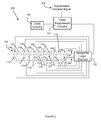
- FIG. 1 illustrates an example bidirectional Gray code counter 100 , according to various embodiments.
- the Gray code counter 100 may count in binary reflected Gray code.
- the bidirectional Gray code counter 100 may include a sequential logic element 102 to store a Gray code value of the bidirectional Gray code counter 100 .
- the sequential logic element 102 may include registers, flip-flops, latches, other electrical components capable of storing the Gray code value, or some combination thereof.
- the sequential logic element 102 may store a current Gray code value.
- the sequential logic element 102 may include a number of outputs 101 corresponding to a number of bits in the Gray code value.
- the number of outputs 101 of the sequential logic element 102 may have a one-to-one ratio with the number of bits in the Gray code value.
- the sequential logic element 102 may include a number of inputs 103 corresponding to the number bits in the Gray code value.
- the number of inputs 103 may have a one-to-one ratio with the number of bits in the Gray code value.
- the inputs 103 may include an input corresponding to a MSB position of the Gray code value, an input corresponding to a LSB position of the Gray code value, and/or one or more inputs corresponding to bit positions of the Gray code value that have significance levels between the MSB and the LSB.
- the inputs 103 may receive input logic levels and/or voltages corresponding to a Gray code value that the sequential logic element 102 stores in response to an update operation.
- the update operation may be initiated by a trigger detected by the sequential logic element 102 .
- the trigger may include a trigger internal to the sequential logic element 102 , such as through a clock internal to the sequential logic element wherein a rising edge, a falling edge, and/or a change in state of the clock that is utilized as the trigger.
- the sequential logic element 102 may replace the current Gray code value with an updated Gray code value that resides on the inputs 103 at the time of the trigger.
- the sequential logic element 102 may store the updated Gray code value until another trigger is detected and may maintain the outputs 101 at output logic levels and/or voltages corresponding to the updated Gray code value until another trigger is detected.
- the trigger may be provided to the sequential logic element 102 by an optional external source, such as by optional clock circuitry 130 .
- the optional clock circuitry 130 may provide the sequential logic element 102 with a clock signal and the sequential logic element 102 may be triggered by the clock signal, such as by a rising edge, a falling edge, and/or a change of the state of the clock signal.
- the trigger for the update operation may include detection, by the sequential logic element 102 , of a change in one or more input logic levels and/or voltages of the inputs 103 .
- the sequential logic element 102 may store the updated Gray code value that resides on the inputs 103 .
- the sequential logic element 102 may include a delay period, for which the sequential logic element 102 determines if the change in the one or more input logic levels and/or voltages remains in the changed state for the delay period prior to storing the updated Gray code value.
- the bidirectional Gray code counter 100 may include logic circuitry 104 coupled to the sequential logic element 102 .
- the logic circuitry 104 may receive the current Gray code value from the outputs 101 of the sequential logic element 102 and provide the updated Gray code value to the inputs 103 of the sequential logic element 102 to be stored by the sequential logic element 102 in response to an update operation.
- the logic circuitry 104 may update, through performance of an increment or a decrement of the current Gray code value, the current Gray code value to be the updated Gray code value.
- the performance of the increment or the decrement of the current Gray code value to the updated Gray code value may maintain the current Gray code value and/or the updated Gray code value in Gray code format throughout the performance.
- the updated Gray code value provided by the logic circuitry 104 may be a sequential Gray code value to the current Gray code value stored in the sequential logic element 102 .
- the sequential Gray code value may be an incremented Gray code value produced by performance an increment operation on the current Gray code value or may be a decremented Gray code value produced by performance of a decrement operation on the current Gray code value.
- the logic circuitry 104 may perform the increment operation as part of the update of the Gray code value. To perform the increment operation, the logic circuitry 104 may update the LSB stored in the LSB position of the sequential logic element 102 . The logic circuitry 104 may perform a logical exclusive-or operation on bits within the current Gray code value that have a greater significance than the LSB. The logic circuitry 104 may set the updated LSB to be equal to a logical inverse of the resultant value produced by the logical exclusive-or operation.
- the logic circuitry 104 may update, in the increment operation, a bit located adjacent to the LSB (also referred to as bit position g 1 ) within the current Gray code value.
- the logic circuitry 104 may determine whether the LSB of the current Gray code value is a logical one or a logical zero. Based on a determination that the LSB is a logical zero, the logic circuitry 104 may maintain a value of the bit located adjacent to the LSB. Based on a determination that the LSB is a logical one, the logic circuitry 104 may update the bit located adjacent to the LSB.
- the logic circuitry 104 may perform a logical exclusive-or operation on bits within the Gray code value that have a greater significance than the bit adjacent to the LSB.
- the logic circuitry 104 may set the updated bit adjacent to the LSB to be equal to the logical inverse of a resultant value produced by the performance of the logical exclusive-or operation.
- the logic circuitry 104 may update, in the increment operation, upper bits, including the MSB, other than the LSB and the bit located adjacent to the LSB (also referred to as bit positions g 2 through g N-1 ).
- the logic circuitry 104 may determine if a bit within the upper bits is adjacent to a less significant bit that is the least significant logical one of the current Gray code value.
- the logic circuitry 104 may maintain a value of the bit based on a determination that the adjacent, less significant bit is not the least significant logical one of the current Gray code value.
- the logic circuitry 104 may perform a logical exclusive-or operation on bits within the Gray code value that have greater significance than the bit.
- the logic circuitry 104 may set the updated bit to be equal to the logical inverse of the resultant value of the logical exclusive-or operation.
- the logic circuitry 104 may perform the updates of the LSB, the adjacent bit to the LSB, and/or the upper bits concurrently. In some embodiments, the logic circuitry may delay one or more of the updates of the LSB, the adjacent bit to the LSB, and/or the upper bits such that the updates may occur at different times. Further, the update operation performed on the current Gray code value may include one or more of the updates of the LSB, the adjacent bit to the LSB, and/or the upper bits as part of the increment operation applied to the current Gray code value to produce the updated Gray code value.
- the logic circuitry 104 may perform the decrement operation as part of the update of the Gray code value. To perform the decrement operation, the logic circuitry 104 may update the LSB stored in the LSB position of the sequential logic element 102 . The logic circuitry 104 may perform a logical exclusive-or operation on bits within the Gray code value that have greater significance than the LSB (also referred to as g 1 through g N-1 ). The logic circuitry 104 may set the updated LSB to be equal to a resultant value produced by the performance of the logical exclusive-or operation.
- the logic circuitry 104 may update, in the decrement operation, a bit adjacent to the LSB.
- the logic circuitry 104 may determine whether the LSB of the current Gray code is a logical one or a logical zero.
- the logic circuitry 104 may maintain a value of the bit adjacent to the LSB based on a determination that the LSB is a logical zero.
- the logic circuitry 104 may perform a logical exclusive-or operation on bits within the Gray code value that have greater significance than the bit adjacent to the LSB based on a determination that the LSB is a logical one.
- the logic circuitry 104 may set the updated LSB to the resultant value produced by the performance of the logical exclusive-or operation.
- the logic circuitry 104 may update, in the decrement operation, upper bits, including the MSB, of the Gray code value that are not the LSB or the bit adjacent to the LSB.
- the logic circuitry 104 may determine, for a bit of the upper bits, whether an adjacent bit that has less significance than the bit is a least significant logical one of the current Gray code value.
- the logic circuitry 104 may maintain a value of the bit based on a determination that the adjacent, less significant bit is not the least significant logical one.
- the logic circuitry 104 may perform a logical exclusive-or operation on bits within the current Gray code that have a greater significance than the bit based on a determination that the adjacent, less significant bit is the least significant logical one of the Gray code value.
- the logic circuitry 104 may set the updated bit equal to be a resultant value produced by the performance of the logical exclusive-or operation.
- the logic circuitry 104 may include electrical elements, including multiplexers, logical or gates, logical nor gates, logical and gates, logical nand gates, and/or logical inverters, to perform the updates of current Gray code value described above.
- the electrical elements utilized by the logic circuitry 104 for performance of the increment of the current Gray code value may be the same electrical elements utilized by the logic circuitry 104 for performance of the decrement of the current Gray code value.
- the logic circuitry 104 includes a plurality of logic gates, wherein the same logic gates are utilized for performance of the increment of the Gray code value and for performance of the decrement of the Gray code value.
- the logic circuitry 104 may determine whether to provide the incremented Gray code value or the decremented Gray code value as the sequential Gray code value based on a bidirectional indicator signal received by the logic circuitry 104 on an increment line 128 .
- the logic circuitry 104 may provide the incremented Gray code value in response to a determination that the bidirectional indicator signal is in a first state (either a high or low state) and may provide the decremented Gray code value in response to a determination that the bidirectional indicator signal is in a second state (a different state than the first state).
- the logic circuitry 104 may replace the current Gray code value stored in the sequential logic element 102 with the incremented Gray code value or the decremented Gray code value.
- the logic circuitry 104 may identify potential wraparound conditions of the Gray code value and prevent update of the Gray code value in response to the identification of the wraparound conditions.
- the logic circuitry 104 may determine that the Gray code value stored in the sequential logic element is equal to a maximum Gray code value or a minimum Gray code value that can be represented by the bidirectional Gray code counter 100 and prevent the update of the Gray code value in response to the determination.
- the prevention of the update of the Gray code value may be implemented by maintaining the updated Gray code value to be equal to the current Gray code value, in contrast to setting the updated Gray code value to the sequential Gray code value as described above.
- the logic circuitry 104 may include one or more multiplexers, such as multiplexers 106 .
- a number of the multiplexers 106 may correspond to the number of bits in the Gray code value and the number of inputs 103 to the sequential logic element 102 .
- the number of the multiplexers 106 may have a one to one ratio with the number of bits in the Gray code value and/or the number of inputs 103 to the sequential logic element 102 .
- Each of the multiplexers 106 may correspond to a single bit position of the Gray code value, including a multiplexer corresponding to the MSB position of the Gray code value, a multiplexer corresponding to the LSB position of the Gray code value, and/or one or more multiplexers corresponding to bit positions between the MSB position and the LSB position.
- each of the multiplexers 106 may have an output that is coupled to an input of the sequential logic element 102 , wherein the output of the multiplexer 106 and the input of the sequential logic element 102 may correspond to a same bit position of the Gray code value.
- the output of each of multiplexers 106 may provide a logic level and/or voltage to the corresponding input of the sequential logic element 102 , the logic level and/or voltage associated with a logic level and/or voltage of the corresponding bit position of the Gray code value to the output.
- each of the multiplexers 106 may include two inputs. One of the two inputs may be coupled to an output of the sequential logic element 102 , the output of the sequential logic element 102 corresponding to a same bit position of the Gray code value as the bit position to which the multiplexer corresponds.
- the multiplexers 106 may include more than two inputs and one or more of the more than two inputs may be coupled to the output.
- each of the multiplexers 106 may further include a select input.
- the select input may receive a signal that indicates which of the inputs of the corresponding multiplexer should be present at the output of the multiplexer.
- Each of the multiplexers 106 may maintain a logic level and/or voltage on the corresponding output of the multiplexer equal to one of the inputs of the multiplexer based on the signal received on the select input.
- the logic circuitry 104 may include a single multiplexer with multiple inputs, multiple outputs, and/or multiple select inputs with each of the multiple inputs, multiple outputs, and/or multiple select inputs corresponding to an input of the sequential logic element 102 .
- the logic circuitry 104 may include one or more logical exclusive-or gates, including logical exclusive-or gates 110 and logical exclusive-or gates 112 .
- the logical exclusive-or gates 110 may each be associated with a corresponding bit position of the Gray code value.
- the logical exclusive-or gates 110 may correspond to the bit positions from the LSB position of the Gray code value to the g N-3 bit position.
- a logical exclusive-or gate of the logical exclusive-or gates 110 may receive a value of an adjacent bit with greater significance than the bit position corresponding the logical exclusive-or gate and a value/s of the bits of greater significance of the adjacent bit and/or a resultant value of an exclusive-or operation applied to the bits of greater significance of the adjacent bit.
- the logical exclusive-or gate may output a resultant value of an exclusive-or operation applied to the received values.
- the logical exclusive-or gates 112 may each be associated with a corresponding bit position of the Gray code value.
- the logical exclusive-or gates 112 may correspond to bit positions from the LSB position to the g N-2 bit position.
- a logical exclusive-or gate of the logical exclusive-or gates 112 may receive the increment line 128 , that carries the bidirectional indicator signal, and a value of bits with greater significance than the bit position corresponding to the logical exclusive-or gate and/or a resultant value of a logical exclusive-or operation applied to the bits with greater significance.
- the logical exclusive-or gate may output a resultant value of an exclusive-or operation applied to the received values.
- the logical exclusive-or gate may output the resultant value to a corresponding one of the inputs of the multiplexers 106 .
- the logic circuitry 104 may include a logical exclusive-nor gate 114 .
- the logical exclusive-nor gate 114 may correspond to the MSB position of the Gray code value.
- the logical exclusive-nor gate 114 may receive a value of an adjacent bit with lesser significance to the MSB position and the increment line 128 , that carries the bidirectional indicator signal.
- the logical exclusive-nor gate 114 may output a resultant value of a logical exclusive-nor operation applied to the received values.
- the logical exclusive-nor gate 114 may output the resultant value to a corresponding one input of a multiplexer, of the multiplexers 106 , corresponding to the MSB position.
- the logic circuitry 104 may include one or more logical and gates, such as logical and gate 116 , logical and gate 118 , logical and gates 120 , logical and gate 122 , and logical and gates 124 .
- the logical and gate 116 may correspond to the g 1 bit position.
- the logical and gate 116 may receive an update line 126 , that carries an update signal, and a value of the LSB.
- the logical and gate 116 may output a resultant value of a logical and operation applied to the received values.
- the logical and gate 116 may output the resultant value to a select line of the multiplexer 106 that corresponds to the g 1 bit position.
- the multiplexer 106 may utilize the resultant value provided on the select line to determine which of the inputs to the multiplexer is to be output by the multiplexer.
- the logical and gate 118 may correspond to a g 2 bit position.
- the logical and gate 118 may receive an update signal on an update line 126 , a value of the g 1 bit, and a logical inverse of the value of the MSB.
- the logical and gate 118 may output a resultant value of a logical and operation applied to the received values.
- the logical and gate 118 may output the resultant value to a select line of the multiplexer 106 corresponding to the g 2 bit position.
- the multiplexer may utilize the resultant value provided on the select line to determine which of the inputs to the multiplexer is to be output by the multiplexer.
- the logical and gates 120 may correspond to bit positions between the MSB position and the g 2 bit position.
- the individual logical and gates 120 may receive the update signal on update line 126 , a value of the adjacent bit with lesser significance than the bit position corresponding to the logical and gate, and a resultant value of a logical nand operation applied to bits of the current Gray code value with lesser significance than the adjacent bit.
- the logical and gate may output a resultant value of a logical and operation applied to the received values.
- the logical and gate may output the resultant value to a select line of the multiplexer 106 that corresponds to a same bit position as the logical and gate.
- the multiplexer may utilize the resultant value provided on the select line to determine which of the inputs to the multiplexer is to be output by the multiplexer.
- the logical and gate 122 may correspond to the MSB position.
- the logical and gate 122 may receive the update signal on the update line 126 and a resultant value of a logical nand operation applied to bits of the current Gray code value with lesser significance than an adjacent bit, the adjacent bit with lesser significance than the MSB.
- the logical and gate 122 may output a resultant value of a logical and operation applied to the received values.
- the logical and gate 122 may output the resultant value to a select line of the multiplexer 106 corresponding to the MSB position.
- the multiplexer may utilize the resultant value provided on the select line to determine which of the inputs to the multiplexer is to be output by the multiplexer.
- the logical and gates 124 may correspond to the MSB position (g N-1 ) and the g N-2 bit position, respectively, as shown in FIG. 1 .
- the individual logical and gates 124 may receive a resultant value of a logical inverse operation applied to an adjacent bit with less significance than a bit corresponding to the respective logical and gate 124 and a resultant value of a logical nand operation applied to bits with lesser significance than the adjacent bit.
- the logical and gate 124 may output a resultant value of a logical and operation applied to the received bits.
- the logical and gate 124 may output the resultant value to one or more of the logical and gates 120 and/or the logical and gate 122 .
- the logic circuitry 104 may further include a logical nand gate 125 .
- the logical nand gate 125 may correspond to the g 3 bit position.
- the logical nand gate 125 may receive a value of the g 1 bit and a value of the LSB (g 0 ).
- the logical nand gate 125 may output a resultant value of a logical nand operation applied to the received bits.
- the logical nand gate 125 may output the resultant value to one or more of the logical and gates 120 and/or logical and gates 124 .
- the bidirectional Gray code counter 100 is illustrated and described for a six-bit Gray code value, it is to be understood that the bidirectional Gray code counter 100 may be extended or contracted to accommodate greater or fewer bits than illustrated and described.
- the logic circuitry 104 may include more or less electrical elements that have a configuration similar to the configuration of the electrical elements (including the multiplexer, logical and gates, and logical exclusive-or gates) corresponding to the g N-3 bit position as illustrated and described.
- FIG. 2 illustrates an example bidirectional Gray code counter 200 with clock suppression circuitry 202 , according to various embodiments.
- the Gray code counter 200 may count in binary reflected Gray code.
- the bidirectional Gray code counter 200 may include the sequential logic element 102 , the logic circuitry 104 and the clock circuitry 130 as described in relation to the description of FIG. 1 .
- the sequential logic element 102 , the logic circuitry 104 and the clock circuitry 130 may include one or more of the corresponding features described in relation to the description of FIG. 1 .
- the bidirectional Gray code counter 200 may include the clock suppression circuitry 202 .
- the clock suppression circuitry 202 may be coupled between the clock circuitry 130 and the sequential logic element 102 .
- the sequential logic element 102 may be triggered to update a stored Gray code value in the sequential logic element 102 in response to a feature of a clock signal produced by the clock circuitry 130 , such as by a rising edge, a falling edge, and/or a change of the state of the clock signal.
- the clock suppression circuitry 202 may suppress the clock signal and/or maintain a current value of the clock signal, such that the sequential logic element 102 does not receive or detect the feature to trigger the update of the sequential logic element 102 .
- the clock suppression circuitry 202 may receive a suppression indicator signal 204 that indicates whether the clock suppression circuitry 202 is to suppress the clock signal and/or maintain a current value of the clock signal.
- the clock suppression circuitry 202 may determine a state of the suppression indicator signal 204 . In response to determination that the suppression indicator signal 204 is in a first state, the clock suppression circuitry 202 may allow the clock signal to pass from the clock circuitry 130 to the sequential logic element 102 without interruption. In response to determination that the suppression indicator signal 204 is in a second state, different than the first state, the clock suppression circuitry 202 may suppress the clock signal (e.g., prevent the clock signal from passing to the sequential logic element 102 and/or maintain the current value of the clock signal).
- the clock suppression circuitry 202 suppresses the clock signal, the sequential logic element 102 will not be triggered to update the current Gray code value stored by the sequential logic element 102 . Effectively, through suppression of the clock signal, the clock suppression circuitry 202 prevents the bidirectional Gray code counter 200 from counting.
- FIG. 3 illustrates an example bidirectional Gray code counter 300 with update suppression circuitry 302 , according to various embodiments.
- the Gray code counter 300 may count in binary reflected Gray code.
- the bidirectional Gray code counter 200 may include the sequential logic element 102 , the logic circuitry 104 and the clock circuitry 130 as described in relation to the description of FIG. 1 .
- the sequential logic element 102 , the logic circuitry 104 and the clock circuitry 130 may include one or more of the corresponding features described in relation to the description of FIG. 1 .
- the bidirectional Gray code counter 300 may include the update suppression circuitry 302 coupled between an input of the update line 126 , that carries the update signal, and the logic circuitry 104 .
- the update signal may be provided, either directly or indirectly through logic elements, to the respective select lines of the multiplexers 106 of the logic circuitry 104 .
- the individual multiplexer 106 may determine a state of the update signal and select which of the inputs to the multiplexer 106 to provide to the output of the multiplexer 106 based on the state (e.g., logic value) of the update signal. In a first state of the update signal, the multiplexers 106 may provide to the outputs values corresponding to the current Gray code value stored in the sequential logic element 102 .
- the multiplexers 106 may maintain the updated Gray code value as equal to the current Gray code value based on the detection of the one state of the update signal, effectively preventing increment or decrement of the current Gray code value.
- the multiplexers 106 may provide to the outputs values corresponding to an incremented or decremented Gray code value.
- the update suppression circuitry 302 may receive a suppression indicator signal 304 and may determine a state of the suppression indicator signal 304 . Based on a determination that the suppression indicator signal 304 is in a first state, the update suppression circuitry 302 may allow the update signal to pass unaffected to the logic circuitry 104 . Based on a determination that the suppression indicator signal 304 is in a second state, different than the first state, the update suppression circuitry 302 may suppress the update signal. While suppressing the update signal, the update suppression circuitry 302 may maintain the update signal on the update line 126 provided to the logic circuitry 104 in the first state that causes the multiplexers 106 to maintain the updated Gray code value as equal to the current Gray code value. Effectively, the update suppression circuitry 302 prevents the bidirectional Gray code counter 300 from performance of an increment and/or decrement operation.
- the bidirectional Gray code counter 300 may be utilized in combination with one or more of the features of the bidirectional Gray code counter 200 described in relation to FIG. 2 .
- the bidirectional Gray code counter 300 may include the update suppression circuitry 302 , the clock circuitry 130 , and/or the clock suppression circuitry 202 .
- the bidirectional Gray code counter 300 may include one or more of the features associated with the update suppression circuitry 302 , the clock circuitry 130 , and/or the clock suppression circuitry 202 .
- FIG. 4 illustrates an example bidirectional Gray code counter 400 with wrap enablement.
- the Gray code counter 400 may count in binary reflected Gray code.
- the bidirectional Gray code counter 400 may include the sequential logic element 102 , as described in relation to FIG. 1 , to store a Gray code value.
- the bidirectional Gray code counter 400 may include logic circuitry 402 .
- the logic circuitry 402 may perform one or more of the same operations (including the update operation of the current Gray code value) of the logic circuitry 104 , described in relation to FIG. 1 .
- the logic circuitry 402 may include one or more of the electrical elements and/or logic elements of the logic circuitry 104 , including the multiplexers 106 , the logical exclusive-or gates 110 , the logical exclusive-or gates 112 , the logical exclusive-nor gate 114 , the logical and gate 116 , the logical and gate 118 , the logical and gates 120 , the logical and gates 124 , the logical nand gate 125 , or some combination thereof.
- the logic circuitry 402 may receive an enable wrap signal on an EnWrap line 404 .
- the logic circuitry 402 may determine a state of the enable wrap signal and may enable wraparound of the Gray code value by the bidirectional Gray code counter 400 . With the wraparound enabled, the logic circuitry 402 may increment a current Gray code value corresponding to a maximum value representable by the bidirectional Gray code counter 400 to a minimum value representable by the bidirectional Gray code counter 400 and/or may decrement a current Gray code value corresponding to the minimum value to the maximum value.
- the sequential logic element 102 may include a reserved bit for indication that a wraparound has occurred.
- the bidirectional Gray code counter 400 may include a separate sequential element and/or memory device for storage of an indication that a wraparound has occurred, and/or a count of an amount of times that the wraparound has occurred and/or a direction corresponding to each of the wraparounds that occurred.
- the logic circuitry 402 may include a logical or gate 406 .
- the logical or gate 406 may correspond to a MSB position of the Gray code value stored in the sequential logic element 102 .
- the logical or gate 406 may receive the enable wrap signal and a value of the g N-2 bit position of the current Gray code value stored in the sequential logic element 102 .
- the logical or gate 406 may output a resultant value produced by a logical or operation applied to the received values.
- the logic circuitry 402 may include a logical and gate 408 .
- the logical and gate 408 may be used instead of logical and gate 122 of the logic circuitry 104 , described in relation to FIG. 1 .
- the logical and gate 408 may correspond to the MSB position of the Gray code value.
- the logical and gate 408 may receive the update signal on the update line 126 , a resultant value of a logical nand operation applied to bits with lesser significance than the g N-2 bit position and the resultant value output by the logical or gate 406 .
- the logical and gate 408 may output a resultant value produced by a logical and operation applied to the received values.
- the logical and gate 408 may output the resultant value to the select line of the multiplexer 106 corresponding to the MSB position.
- the multiplexer may utilize the resultant value provided to the select line to select which of the values on the inputs of the multiplexer should be output from the multiplexer.
- the bidirectional Gray code counter 400 may be utilized in combination with one or more of the features of the bidirectional Gray code counter 200 , described in relation to FIG. 2 , and/or of the bidirectional Gray code counter 300 , described in relation to FIG. 3 .
- the bidirectional Gray code counter 400 may include one or more of the elements selected from the group of elements including the update suppression circuitry 302 , and the clock circuitry 130 , the clock suppression circuitry 202 , and/or the elements associated with the wrap enable.
- the bidirectional Gray code counter 400 may include one or more of the features associated with the update suppression circuitry 302 , the clock circuitry 130 , the clock suppression circuitry 202 , and/or the wrap enable function.
- FIG. 5 illustrates an example bidirectional Gray code counter 500 with stepped bidirectional indicator signal.
- the bidirectional Gray code counter 500 may include the sequential logic element 102 , as described in relation to FIG. 1 , to store a Gray code value.
- the bidirectional Gray code counter 500 may include logic circuitry 502 .
- the Gray code counter 500 may count in binary reflected Gray code.
- the logic circuitry 502 may perform one or more of the same operations (including the update operation of the current Gray code value) of the logic circuitry 104 , described in relation to FIG. 1 .
- the logic circuitry 502 may include one or more of the electrical elements and/or logic elements of the logic circuitry 104 , including the multiplexers 106 , the logical exclusive-or gates 112 , the logical exclusive-nor gate 114 , the logical and gate 116 , the logical and gate 118 , the logical and gates 120 , the logical and gates 124 , the logical nand gate 125 , or some combination thereof.
- the logic circuitry 502 may include a logical exclusive-or gate 112 corresponding to the g N-2 bit position.
- the logical exclusive-or gate 112 may receive the MSB of the Gray code value and a bidirectional indicator signal, transmitted on the increment line 128 .
- the logical exclusive-or gate 112 may output a resultant value produced by performance of a logical exclusive-or operation on the received values.
- the logical exclusive-or gate 112 may output the resultant value to an input of the multiplexer that corresponds to the g N-2 bit position.
- the logic circuitry 502 may include one or more logical exclusive-or gates 504 .
- Each of the logical exclusive-or gates 504 may correspond to a bit position of the Gray code value stored in the sequential logic element 102 .
- the logical exclusive-or gates 504 may correspond to bit positions from the LSB position to the g N-3 bit position.
- Each of the logical exclusive-or gates 504 may receive a value of the bit in the corresponding bit position to the logical exclusive-or gate.
- Each of the logical exclusive-or gates 504 may further receive a resultant value produced by the exclusive-or gate 112 or another of the logical exclusive-or gates corresponding to an adjacent bit position with greater significance than the corresponding bit position.
- Each of the logical exclusive-or gates 504 may output a resultant value produced by performance of a logical exclusive-or operation on the received values. Each of the logical exclusive-or gates 504 may output the resultant value to an input of the multiplexer corresponding to the same bit position.
- the logic circuitry 502 may effectively step the bidirectional indicator signal through the logical exclusive-or gate 112 and/or the logical exclusive-or gates 504 .
- the logic circuitry 502 may be utilized in applications where transmission time of the bidirectional indicator signal is not critical. In some embodiments, the logic circuitry may utilize less logic gates than the other logic circuitry described above and, therefore consume less power.
- the bidirectional Gray code counter 500 may be utilized in combination with one or more of the features of the bidirectional Gray code counter 200 , described in relation to FIG. 2 , of the bidirectional Gray code counter 300 , described in relation to FIG. 3 , and/or of the bidirectional Gray code counter 400 , described in relation to FIG. 4 .
- the bidirectional Gray code counter 500 may include one or more of the elements selected from the group of elements including the update suppression circuitry 302 , and the clock circuitry 130 , the clock suppression circuitry 202 , the elements associated with the wrap enable, and/or the elements associated with the stepped bidirectional indicator signal.
- the bidirectional Gray code counter 500 may include one or more of the features associated with the update suppression circuitry 302 , the clock circuitry 130 , the clock suppression circuitry 202 , the wrap enable function, and/or the stepped bidirectional indicator signal.
- Performance of an increment from one Gray code value to the subsequent Gray code value may be performed by transforming the Gray code value into binary and using the binary equivalent for increment to the subsequent Gray code value.
- h i P i+1 (P i+1 g i )Z i ⁇ 1 P i (P i g i ⁇ 1 )Z i ⁇ 2 .
- h i may be separated into two cases based on Z i ⁇ 2 , represented by
- the two subcases may be represented by
- FIG. 6 illustrates an example computing device 600 that may employ the apparatuses and/or methods described herein (e.g., the bidirectional Gray code counter 100 , the bidirectional Gray code counter 200 , the bidirectional Gray code counter 300 , the bidirectional Gray code counter 400 and/or the bidirectional Gray code counter 500 ), in accordance with various embodiments.
- computing device 600 may include a number of components, such as one or more processor(s) 604 (one shown) and at least one communication chip 606 .
- the one or more processor(s) 604 each may include one or more processor cores.
- the at least one communication chip 606 may be physically and electrically coupled to the one or more processor(s) 604 .
- the communication chip 606 may be part of the one or more processor(s) 604 .
- computing device 600 may include printed circuit board (PCB) 602 .
- PCB printed circuit board
- the one or more processor(s) 604 and communication chip 606 may be disposed thereon.
- the various components may be coupled without the employment of PCB 602 .
- computing device 600 may include other components that may or may not be physically and electrically coupled to the PCB 602 .
- these other components include, but are not limited to, memory controller 626 , volatile memory (e.g., dynamic random access memory (DRAM) 620 ), non-volatile memory such as read only memory (ROM) 624 , flash memory 622 , storage device 654 (e.g., a hard-disk drive (HDD)), an I/O controller 641 , a digital signal processor (not shown), a crypto processor (not shown), a graphics processor 630 , one or more antenna 628 , a display (not shown), a touch screen display 632 , a touch screen controller 646 , a battery 636 , an audio codec (not shown), a video codec (not shown), a global positioning system (GPS) device 640 , a compass 642 , an accelerometer (not shown), a gyroscope (not shown), a speaker 650 ,
- the one or more processor(s) 604 , flash memory 622 , and/or storage device 654 may include associated firmware (not shown) storing programming instructions configured to enable computing device 600 , in response to execution of the programming instructions by one or more processor(s) 604 , to practice all or selected aspects of the methods described herein. In various embodiments, these aspects may additionally or alternatively be implemented using hardware separate from the one or more processor(s) 604 , flash memory 622 , or storage device 654 .
- one or more components of the computing device 600 may include the bidirectional Gray code counter 100 , the bidirectional Gray code counter 200 , the bidirectional Gray code counter 300 , the bidirectional Gray code counter 400 , and/or the bidirectional Gray code counter 500 described herein.
- the bidirectional Gray code counter 100 , the bidirectional Gray code counter 200 , the bidirectional Gray code counter 300 , the bidirectional Gray code counter 400 , and/or the bidirectional Gray code counter 500 , and/or the processing circuitry 600 may be included in I/O controller 641 , processor 604 , memory controller 626 , and/or another component of computing device 600 .
- the communication chips 606 may enable wired and/or wireless communications for the transfer of data to and from the computing device 600 .
- wireless and its derivatives may be used to describe circuits, devices, systems, methods, techniques, communications channels, etc., that may communicate data through the use of modulated electromagnetic radiation through a non-solid medium. The term does not imply that the associated devices do not contain any wires, although in some embodiments they might not.
- the communication chip 606 may implement any of a number of wireless standards or protocols, including but not limited to IEEE 602.20, Long Term Evolution (LTE), LTE Advanced (LTE-A), General Packet Radio Service (GPRS), Evolution Data Optimized (Ev-DO), Evolved High Speed Packet Access (HSPA+), Evolved High Speed Downlink Packet Access (HSDPA+), Evolved High Speed Uplink Packet Access (HSUPA+), Global System for Mobile Communications (GSM), Enhanced Data rates for GSM Evolution (EDGE), Code Division Multiple Access (CDMA), Time Division Multiple Access (TDMA), Digital Enhanced Cordless Telecommunications (DECT), Worldwide Interoperability for Microwave Access (WiMAX), Bluetooth, derivatives thereof, as well as any other wireless protocols that are designated as 3G, 4G, 5G, and beyond.
- IEEE 602.20 Long Term Evolution (LTE), LTE Advanced (LTE-A), General Packet Radio Service (GPRS), Evolution Data Optimized (Ev-DO),
- the computing device 600 may include a plurality of communication chips 606 .
- a first communication chip 606 may be dedicated to shorter range wireless communications such as Wi-Fi and Bluetooth
- a second communication chip 606 may be dedicated to longer range wireless communications such as GPS, EDGE, GPRS, CDMA, WiMAX, LTE, Ev-DO, and others.
- the computing device 600 may be a laptop, a netbook, a notebook, an ultrabook, a smartphone, a computing tablet, a personal digital assistant (PDA), an ultra-mobile PC, a mobile phone, a desktop computer, a server, a printer, a scanner, a monitor, a set-top box, an entertainment control unit (e.g., a gaming console or automotive entertainment unit), a digital camera, an appliance, a portable music player, or a digital video recorder.
- the computing device 600 may be any other electronic device that processes data.
- Example 4 may include the bidirectional gray code counter of any of the examples 1 and 2, wherein the logic circuitry is to further determine that the gray code value stored in the sequential logic element is equal to a minimum gray code value that can be represented by the bidirectional gray code counter and prevent, based on the determination that the gray code value is equal to the minimum gray code value, the update, through the performance of the decrement, of the gray code value.
- Example 5 may include the bidirectional gray code counter of any of the examples 1 and 2, wherein, to update, through performance of the increment of the gray code value, the gray code value, the logic circuitry is to update a least significant bit of the gray code value to be a logical inverse of a resultant value produced by performance of a logical exclusive-or operation on bits, within the gray code value, of greater significance than the least significant bit.
- Example 6 may include the bidirectional gray code counter of any of the examples 1 and 2, wherein, to update, through performance of the increment of the gray code value, the gray code value, the logic circuitry is to determine whether a least significant bit of the gray code value is a logical one or a logical zero and maintain, based on determination that the least significant bit is a logical zero, a value of a bit adjacent to the least significant bit.
- Example 7 may include the bidirectional gray code counter of any of the examples 1 and 2, wherein, to update, through performance of the increment of the gray code value, the gray code value, the logic circuitry is to determine whether a least significant bit of the gray code value is a logical one or a logical zero and update, based on determination that the least significant bit is a logical one, a bit adjacent to the least significant bit to be a logical inverse of a resultant value produced by performance of a logical exclusive-or operation on bits, within the gray code value, of greater significance than the bit adjacent to the least significant bit.
- Example 9 may include the bidirectional gray code counter of any of the examples 1 and 2, wherein, to update, through performance of the increment of the gray code value, the gray code value, the logic circuitry is to determine, for an individual bit of the gray code value that is not a least significant bit of the gray-code value and not adjacent to the least significant bit, whether an adjacent, less significant bit is a least significant logical one of the gray code value and if the adjacent, less significant bit is determined to be least significant logical one, update the individual bit to be a logical inverse of a resultant value produced by performance of a logical exclusive-or operation on bits, within the gray code value, of greater significance than the individual bit.
- Example 10 may include the bidirectional gray code counter of any of the examples 1 and 2, wherein, to update, through performance of the decrement of the gray code value, the gray code value, the logic circuitry is to update a least significant bit of the gray code value to be a resultant value produced by performance of a logical exclusive-or operation on bits, within the gray code value, of greater significance than the least significant bit.
- Example 11 may include the bidirectional gray code counter of any of the examples 1 and 2, wherein, to update, through performance of the decrement of the gray code value, the gray code value, the logic circuitry is to determine whether a least significant bit of the gray code value is a logical one or a logical zero and if the least significant bit is determined to be the logical zero, maintain a value of a bit adjacent to the least significant bit.
- Example 12 may include the bidirectional gray code counter of any of the examples 1 and 2, wherein, to update, through performance of the decrement of the gray code value, the gray code value, the logic circuitry is to determine whether a least significant bit of the gray code value is a logical one or a logical zero and if the least significant bit is determined to be a logical one, update a bit adjacent to the least significant bit to be a resultant value produced by performance of a logical exclusive-or operation on bits, within the gray code value, of greater significance than the bit adjacent to the least significant bit.
- Example 13 may include the bidirectional gray code counter of any of the examples 1 and 2, wherein, to update, through performance of the decrement of the gray code value, the gray code value, the logic circuitry is to determine, for an individual bit of the gray code value that is not a least significant bit of the gray-code value and not adjacent to the least significant bit, whether an adjacent, less significant bit is a least significant logical one of the gray code value and if the adjacent, less significant bit is determined not to be the least significant logical one, maintain a value of the individual bit.
- Example 14 may include the bidirectional gray code counter of any of the examples 1 and 2, wherein, to update, through performance of the decrement of the gray code value, the gray code value, the logic circuitry is to determine, for an individual bit of the gray code value that is not a least significant bit of the gray-code value and not adjacent to the least significant bit, whether an adjacent, less significant bit is a least significant logical one of the gray code value and if the adjacent, less significant bit is determined to be the least significant logical one, update the individual bit to be a resultant value produced by performance of logical exclusive-or operation on bits, within the gray code value, of greater significance than the individual bit.
- Example 15 may include the bidirectional gray code counter of any of the examples 1 and 2, wherein the logic circuitry includes a plurality of logic gates, wherein the same logic gates are utilized for performance of the increment of the gray code value and for performance of the decrement of the gray code value.
- Example 16 may include the bidirectional gray code counter of any of the examples 1 and 2, wherein the logic circuitry includes one or more multiplexers, wherein each multiplexer, of the one or more multiplexers, is associated with a respective bit of the gray code value, and wherein, to update the gray code value, the logic circuitry is to: determine, for each multiplexer whether a respective selection input receives a logical one or a logical zero, for each multiplexer that is determined to receive the logical one at the respective selection input, update a value of the respective bit associated with the respective multiplexer that is determined to receive the logical one and for each multiplexer that is determined to receive the logical zero at the respective selection input, maintain a value of the respective bit associated with the respective multiplexer that is determined to receive the logical zero.
- Example 17 may include the bidirectional gray code counter of any of the examples 1 and 2, wherein the logic circuitry is to further detect a wrap enablement signal and enable wraparound of a count of the bidirectional gray code counter in response to detection of the wrap enablement signal.
- Example 18 may include an apparatus to bidirectionally count in gray code, comprising means to store of a gray code value means to determine whether to perform an increment or a decrement of the gray code value based on a bidirectional indicator signal, the gray code value to a sequential gray code value and means to perform the increment or the decrement of the gray code value, wherein the means to perform maintains the gray code value in gray code format throughout the performance of the increment or the decrement.
- Example 19 may include the apparatus of example 18, further comprising means to update the gray code value in the means for storage with the incremented or the decremented gray code value.
- Example 20 may include the apparatus of any of the examples 18 and 19, further comprising means to determine that the stored gray code value is equal to a maximum gray code value representable by the apparatus and means to prevent, based on the determination that the stored gray code value is equal to the maximum gray code value, the performance of the increment of the gray code value.
- Example 21 may include the apparatus of any of the examples 18 and 19, further comprising means to determine that the stored gray code value is equal to a minimum gray code value representable by the apparatus and means to prevent, based on the determination that the stored gray code value is equal to the minimum gray code value, the performance of the decrement of the gray code value.
- Example 22 may include the apparatus of any of the examples 18 and 19, further comprising means to perform a logical exclusive-or operation on bits, within the gray code value, of greater significance than a least significant bit within the gray code value and means to set the least significant bit of the gray code value to be a logical inverse of a result of the logical exclusive-or operation.
- Example 23 may include the apparatus of example any of the examples 18 and 19, further comprising means to determine whether a least significant bit of the gray code value is a logical one or a logical zero and means to maintain, based on determination that the least significant bit is a logical zero, a value of a bit adjacent to the least significant bit.
- Example 24 may include the apparatus of example any of the examples 18 and 19, further comprising means to determine whether a least significant bit of the gray code value is a logical one or a logical zero, means to perform a logical exclusive-or operation on bits, within the gray code value, of greater significance than a bit adjacent to the least significant bit and means to set, based on determination that the least significant bit of is the logical one, the bit adjacent to the least significant bit to be a logical inverse of a result of the logical exclusive-or operation.
- Example 26 may include the apparatus of any of the examples 18 and 19, further comprising means to determine, for an individual bit of the gray code value that is not a least significant bit of the gray code value and not adjacent to the least significant bit, whether an adjacent, less significant bit is a least significant logical one of the gray code value, means to perform a logical exclusive-or operation on bits, within the gray code value, of greater significance than the individual bit and means to set, based on determination that the adjacent, less significant bit is the least significant logical one, the individual bit to be a logical inverse of a result of the logical exclusive-or operation.
- Example 28 may include the apparatus of any of the examples 18 and 19, further comprising means to determine that a least significant bit of the gray code value is a logical zero and means to maintain, based on determination that the least significant bit is a logical zero, a value of a bit adjacent to the least significant bit.
- Example 29 may include the apparatus of any of the examples 18 and 19, further comprising means to determine that a least significant bit of the gray code value is a logical one, means to perform a logical exclusive-or operation on bits, within the gray code value, of greater significance than a bit adjacent to the least significant bit and means to set, based on determination that the least significant bit is a logical one, the bit adjacent to the least significant bit to be a result of the logical exclusive-or operation.
- Example 31 may include the apparatus of any of the examples 18 and 19, further comprising means to determine, for an individual bit of the gray code value that is not a least significant bit of the gray code value and not adjacent to the least significant bit, that an adjacent, less significant bit is a least significant logical one of the gray code value, means to perform a logical exclusive-or operation on bits, within the gray code value, of greater significance than the individual bit and means to set, based on determination that the adjacent, less significant bit is the least significant logical one, the individual bit to be a result of the logical exclusive-or operation.
- Example 33 may include the apparatus of any of the examples 18 and 19, further comprising means to detect a wrap enablement signal and means to enable wraparound of a count associated with the apparatus in response to detection of the wrap enablement signal.
- Example 35 may include the system of example 34, further comprising a processor that includes the sequential logic element, the one or more multiplexer, and the logic circuitry, a network interface, and one or more input/output ports of the network interface coupled to the processor.
- Example 37 may include the system of any of the examples 34-36, wherein the logic circuitry includes one or more logical and gates, each of the one or more logical and gates coupled to a respective select input of a respective multiplexer from the one or more multiplexers, wherein each of the one or more logical and gates is associated with a respective bit of the gray code value, and wherein the logical and gates are to receive an update signal, a value of an adjacent, less significant bit of the gray code value to the respective bit and a result of a logical nand operation applied to bits, within the gray code value, of less significance than the adjacent, less significant bit and output a select value to the respective select input that is to cause the respective multiplexer to update or maintain the respective bit based on the select value.
- the logic circuitry includes one or more logical and gates, each of the one or more logical and gates coupled to a respective select input of a respective multiplexer from the one or more multiplexers, wherein each of the one or more logical and gates is associated with a
- Example 38 may include the system of example 37, further comprising suppression circuitry to suppress the update signal.
- Example 40 may include the system of example 39, further comprising suppression circuitry to suppress the clock signal.
Landscapes
- Control Of Indicators Other Than Cathode Ray Tubes (AREA)
Abstract
Description
The binary-to-Gray code conversion to produce the incremented Gray code value may be produced by hi=ci+1
Therefore, hi=Pi+1
Further, hi may be separated into two subcases based on gi−1, remembering that gi−1=1→Zi−1=0. The two subcases may be represented by
This derived increment operation can be reversed into a decrement operation by flipping the direction of the bit change illustrated above.
Claims (25)
Priority Applications (1)
| Application Number | Priority Date | Filing Date | Title |
|---|---|---|---|
| US15/146,483 US10439617B2 (en) | 2016-05-04 | 2016-05-04 | Bidirectional gray code counter |
Applications Claiming Priority (1)
| Application Number | Priority Date | Filing Date | Title |
|---|---|---|---|
| US15/146,483 US10439617B2 (en) | 2016-05-04 | 2016-05-04 | Bidirectional gray code counter |
Publications (2)
| Publication Number | Publication Date |
|---|---|
| US20170324415A1 US20170324415A1 (en) | 2017-11-09 |
| US10439617B2 true US10439617B2 (en) | 2019-10-08 |
Family
ID=60244225
Family Applications (1)
| Application Number | Title | Priority Date | Filing Date |
|---|---|---|---|
| US15/146,483 Active 2038-01-28 US10439617B2 (en) | 2016-05-04 | 2016-05-04 | Bidirectional gray code counter |
Country Status (1)
| Country | Link |
|---|---|
| US (1) | US10439617B2 (en) |
Cited By (1)
| Publication number | Priority date | Publication date | Assignee | Title |
|---|---|---|---|---|
| US11342922B1 (en) | 2020-12-21 | 2022-05-24 | Advanced Micro Devices, Inc. | Direct bi-directional gray code counter |
Citations (9)
| Publication number | Priority date | Publication date | Assignee | Title |
|---|---|---|---|---|
| US5164968A (en) * | 1991-10-15 | 1992-11-17 | Loral Aerospace Corp. | Nine bit Gray code generator |
| US5754614A (en) * | 1997-04-03 | 1998-05-19 | Vlsi Technology, Inc. | Gray code counter |
| US6314154B1 (en) * | 1999-11-04 | 2001-11-06 | Vlsi Technology, Inc | Non-power-of-two Gray-code counter and binary incrementer therefor |
| US20050129167A1 (en) * | 2003-12-11 | 2005-06-16 | Heimbigner Gary L. | Gray code counter |
| US20080224904A1 (en) * | 2007-03-15 | 2008-09-18 | Epson Imaging Devices Corporation | Gray code counter and display device therewith |
| US7991104B1 (en) * | 2010-04-29 | 2011-08-02 | Dialog Semiconductor Gmbh | Modular low power gray code counter |
| US8867694B1 (en) * | 2013-07-19 | 2014-10-21 | Freescale Semiconductor, Inc. | Modular gray code counter |
| US20150244376A1 (en) * | 2014-02-26 | 2015-08-27 | Taiwan Semiconductor Manufacturing Company Limited | Gray code counter |
| US9455717B2 (en) * | 2014-01-23 | 2016-09-27 | Dialog Semiconductor (Uk) Limited | Digital counter comprising reduced transition density |
-
2016
- 2016-05-04 US US15/146,483 patent/US10439617B2/en active Active
Patent Citations (9)
| Publication number | Priority date | Publication date | Assignee | Title |
|---|---|---|---|---|
| US5164968A (en) * | 1991-10-15 | 1992-11-17 | Loral Aerospace Corp. | Nine bit Gray code generator |
| US5754614A (en) * | 1997-04-03 | 1998-05-19 | Vlsi Technology, Inc. | Gray code counter |
| US6314154B1 (en) * | 1999-11-04 | 2001-11-06 | Vlsi Technology, Inc | Non-power-of-two Gray-code counter and binary incrementer therefor |
| US20050129167A1 (en) * | 2003-12-11 | 2005-06-16 | Heimbigner Gary L. | Gray code counter |
| US20080224904A1 (en) * | 2007-03-15 | 2008-09-18 | Epson Imaging Devices Corporation | Gray code counter and display device therewith |
| US7991104B1 (en) * | 2010-04-29 | 2011-08-02 | Dialog Semiconductor Gmbh | Modular low power gray code counter |
| US8867694B1 (en) * | 2013-07-19 | 2014-10-21 | Freescale Semiconductor, Inc. | Modular gray code counter |
| US9455717B2 (en) * | 2014-01-23 | 2016-09-27 | Dialog Semiconductor (Uk) Limited | Digital counter comprising reduced transition density |
| US20150244376A1 (en) * | 2014-02-26 | 2015-08-27 | Taiwan Semiconductor Manufacturing Company Limited | Gray code counter |
Cited By (1)
| Publication number | Priority date | Publication date | Assignee | Title |
|---|---|---|---|---|
| US11342922B1 (en) | 2020-12-21 | 2022-05-24 | Advanced Micro Devices, Inc. | Direct bi-directional gray code counter |
Also Published As
| Publication number | Publication date |
|---|---|
| US20170324415A1 (en) | 2017-11-09 |
Similar Documents
| Publication | Publication Date | Title |
|---|---|---|
| US10027472B2 (en) | Non-linear physically unclonable function (PUF) circuit with machine-learning attack resistance | |
| EP3274907B1 (en) | A stable probing-resilient physically unclonable function (puf) circuit | |
| US9847721B2 (en) | Driving circuit, voltage converter having adaptive dead time control function and method of controlling dead time | |
| US9288019B2 (en) | Apparatuses, methods, and systems for jitter equalization and phase error detection | |
| US9369277B2 (en) | Encryption code generation using spin-torque NANO-oscillators | |
| US9502104B2 (en) | Multi-level cell (MLC) non-volatile memory data reading method and apparatus | |
| US9059693B2 (en) | Clock gating circuit | |
| US9160317B2 (en) | Semiconductor circuit and method of operating the same | |
| KR20150115382A (en) | Memory device of adaptively calibrating timing margin and integrated circuit including the same | |
| US10656916B2 (en) | Random number generator including entropy source | |
| US10038451B2 (en) | All digital phase locked loop | |
| KR20200141173A (en) | Read clock generation circuit and data processing circuit including the same | |
| US10193537B2 (en) | Random data generation circuit, memory storage device and random data generation method | |
| US10439617B2 (en) | Bidirectional gray code counter | |
| WO2015088567A1 (en) | Data receiver circuit with offset edge samplers | |
| US20180191347A1 (en) | Voltage level shifter monitor with tunable voltage level shifter replica circuit | |
| EP3353967B1 (en) | Pulsed decision feedback equalization circuit | |
| US9860017B2 (en) | Method of generating data | |
| US9882565B2 (en) | Buffer circuit and electric system including the same | |
| US8601040B2 (en) | Reduced-level shift overflow detection | |
| US10685688B2 (en) | Low swing bitline for sensing arrays | |
| US12107578B1 (en) | Thin-oxide voltage level shifter | |
| US9692400B2 (en) | Pulse width widener and a memory system including the same | |
| US9048875B2 (en) | Conserving computing resources during error correction | |
| CN113129945A (en) | Memory system, electronic device and method of operating memory device |
Legal Events
| Date | Code | Title | Description |
|---|---|---|---|
| AS | Assignment |
Owner name: INTEL CORPORATION, CALIFORNIA Free format text: ASSIGNMENT OF ASSIGNORS INTEREST;ASSIGNOR:NEIDENGARD, MARK L.;REEL/FRAME:038608/0965 Effective date: 20160429 |
|
| STCT | Information on status: administrative procedure adjustment |
Free format text: PROSECUTION SUSPENDED |
|
| STPP | Information on status: patent application and granting procedure in general |
Free format text: NOTICE OF ALLOWANCE MAILED -- APPLICATION RECEIVED IN OFFICE OF PUBLICATIONS |
|
| STPP | Information on status: patent application and granting procedure in general |
Free format text: NOTICE OF ALLOWANCE MAILED -- APPLICATION RECEIVED IN OFFICE OF PUBLICATIONS |
|
| STPP | Information on status: patent application and granting procedure in general |
Free format text: PUBLICATIONS -- ISSUE FEE PAYMENT VERIFIED |
|
| STCF | Information on status: patent grant |
Free format text: PATENTED CASE |
|
| MAFP | Maintenance fee payment |
Free format text: PAYMENT OF MAINTENANCE FEE, 4TH YEAR, LARGE ENTITY (ORIGINAL EVENT CODE: M1551); ENTITY STATUS OF PATENT OWNER: LARGE ENTITY Year of fee payment: 4 |