US10434794B2 - Optical print head and image forming device - Google Patents
Optical print head and image forming device Download PDFInfo
- Publication number
- US10434794B2 US10434794B2 US15/902,644 US201815902644A US10434794B2 US 10434794 B2 US10434794 B2 US 10434794B2 US 201815902644 A US201815902644 A US 201815902644A US 10434794 B2 US10434794 B2 US 10434794B2
- Authority
- US
- United States
- Prior art keywords
- light source
- source substrate
- region
- support portion
- print head
- Prior art date
- Legal status (The legal status is an assumption and is not a legal conclusion. Google has not performed a legal analysis and makes no representation as to the accuracy of the status listed.)
- Expired - Fee Related, expires
Links
- 230000003287 optical effect Effects 0.000 title claims abstract description 74
- 239000000758 substrate Substances 0.000 claims abstract description 110
- 239000000463 material Substances 0.000 claims description 18
- 239000011521 glass Substances 0.000 description 42
- 108091008695 photoreceptors Proteins 0.000 description 23
- 229920001296 polysiloxane Polymers 0.000 description 12
- 229920005989 resin Polymers 0.000 description 10
- 239000011347 resin Substances 0.000 description 10
- 230000004048 modification Effects 0.000 description 7
- 238000012986 modification Methods 0.000 description 7
- 230000006866 deterioration Effects 0.000 description 6
- 238000005516 engineering process Methods 0.000 description 6
- 238000007789 sealing Methods 0.000 description 6
- 230000005611 electricity Effects 0.000 description 5
- 230000001629 suppression Effects 0.000 description 5
- 238000006243 chemical reaction Methods 0.000 description 4
- 238000004140 cleaning Methods 0.000 description 4
- 239000003086 colorant Substances 0.000 description 3
- 230000000694 effects Effects 0.000 description 3
- 239000002184 metal Substances 0.000 description 3
- 229910052751 metal Inorganic materials 0.000 description 3
- 229920000515 polycarbonate Polymers 0.000 description 3
- 239000004417 polycarbonate Substances 0.000 description 3
- 239000003566 sealing material Substances 0.000 description 3
- 238000005452 bending Methods 0.000 description 2
- 238000006073 displacement reaction Methods 0.000 description 2
- 229920006351 engineering plastic Polymers 0.000 description 2
- 239000003365 glass fiber Substances 0.000 description 2
- 239000004519 grease Substances 0.000 description 2
- 230000017525 heat dissipation Effects 0.000 description 2
- 239000007769 metal material Substances 0.000 description 2
- 230000002093 peripheral effect Effects 0.000 description 2
- 230000009467 reduction Effects 0.000 description 2
- 229920003002 synthetic resin Polymers 0.000 description 2
- 239000000057 synthetic resin Substances 0.000 description 2
- 239000010409 thin film Substances 0.000 description 2
- 229920000106 Liquid crystal polymer Polymers 0.000 description 1
- 239000004977 Liquid-crystal polymers (LCPs) Substances 0.000 description 1
- 239000004793 Polystyrene Substances 0.000 description 1
- 229910000831 Steel Inorganic materials 0.000 description 1
- 229920000122 acrylonitrile butadiene styrene Polymers 0.000 description 1
- 239000004676 acrylonitrile butadiene styrene Substances 0.000 description 1
- 239000000853 adhesive Substances 0.000 description 1
- 230000001070 adhesive effect Effects 0.000 description 1
- 238000004891 communication Methods 0.000 description 1
- 238000010586 diagram Methods 0.000 description 1
- 239000000428 dust Substances 0.000 description 1
- 230000007257 malfunction Effects 0.000 description 1
- 238000005555 metalworking Methods 0.000 description 1
- 238000000034 method Methods 0.000 description 1
- 238000000465 moulding Methods 0.000 description 1
- 229920002223 polystyrene Polymers 0.000 description 1
- 230000008569 process Effects 0.000 description 1
- 239000012744 reinforcing agent Substances 0.000 description 1
- 239000004065 semiconductor Substances 0.000 description 1
- 229910001220 stainless steel Inorganic materials 0.000 description 1
- 239000010935 stainless steel Substances 0.000 description 1
- 239000010959 steel Substances 0.000 description 1
Images


Classifications
-
- B—PERFORMING OPERATIONS; TRANSPORTING
- B41—PRINTING; LINING MACHINES; TYPEWRITERS; STAMPS
- B41J—TYPEWRITERS; SELECTIVE PRINTING MECHANISMS, i.e. MECHANISMS PRINTING OTHERWISE THAN FROM A FORME; CORRECTION OF TYPOGRAPHICAL ERRORS
- B41J2/00—Typewriters or selective printing mechanisms characterised by the printing or marking process for which they are designed
- B41J2/435—Typewriters or selective printing mechanisms characterised by the printing or marking process for which they are designed characterised by selective application of radiation to a printing material or impression-transfer material
- B41J2/447—Typewriters or selective printing mechanisms characterised by the printing or marking process for which they are designed characterised by selective application of radiation to a printing material or impression-transfer material using arrays of radiation sources
- B41J2/45—Typewriters or selective printing mechanisms characterised by the printing or marking process for which they are designed characterised by selective application of radiation to a printing material or impression-transfer material using arrays of radiation sources using light-emitting diode [LED] or laser arrays
- B41J2/451—Special optical means therefor, e.g. lenses, mirrors, focusing means
-
- G—PHYSICS
- G03—PHOTOGRAPHY; CINEMATOGRAPHY; ANALOGOUS TECHNIQUES USING WAVES OTHER THAN OPTICAL WAVES; ELECTROGRAPHY; HOLOGRAPHY
- G03G—ELECTROGRAPHY; ELECTROPHOTOGRAPHY; MAGNETOGRAPHY
- G03G15/00—Apparatus for electrographic processes using a charge pattern
- G03G15/04—Apparatus for electrographic processes using a charge pattern for exposing, i.e. imagewise exposure by optically projecting the original image on a photoconductive recording material
- G03G15/04036—Details of illuminating systems, e.g. lamps, reflectors
- G03G15/04045—Details of illuminating systems, e.g. lamps, reflectors for exposing image information provided otherwise than by directly projecting the original image onto the photoconductive recording material, e.g. digital copiers
- G03G15/04054—Details of illuminating systems, e.g. lamps, reflectors for exposing image information provided otherwise than by directly projecting the original image onto the photoconductive recording material, e.g. digital copiers by LED arrays
-
- B—PERFORMING OPERATIONS; TRANSPORTING
- B41—PRINTING; LINING MACHINES; TYPEWRITERS; STAMPS
- B41J—TYPEWRITERS; SELECTIVE PRINTING MECHANISMS, i.e. MECHANISMS PRINTING OTHERWISE THAN FROM A FORME; CORRECTION OF TYPOGRAPHICAL ERRORS
- B41J2/00—Typewriters or selective printing mechanisms characterised by the printing or marking process for which they are designed
- B41J2/435—Typewriters or selective printing mechanisms characterised by the printing or marking process for which they are designed characterised by selective application of radiation to a printing material or impression-transfer material
- B41J2/447—Typewriters or selective printing mechanisms characterised by the printing or marking process for which they are designed characterised by selective application of radiation to a printing material or impression-transfer material using arrays of radiation sources
- B41J2/45—Typewriters or selective printing mechanisms characterised by the printing or marking process for which they are designed characterised by selective application of radiation to a printing material or impression-transfer material using arrays of radiation sources using light-emitting diode [LED] or laser arrays
-
- G—PHYSICS
- G02—OPTICS
- G02B—OPTICAL ELEMENTS, SYSTEMS OR APPARATUS
- G02B7/00—Mountings, adjusting means, or light-tight connections, for optical elements
- G02B7/02—Mountings, adjusting means, or light-tight connections, for optical elements for lenses
-
- G—PHYSICS
- G03—PHOTOGRAPHY; CINEMATOGRAPHY; ANALOGOUS TECHNIQUES USING WAVES OTHER THAN OPTICAL WAVES; ELECTROGRAPHY; HOLOGRAPHY
- G03G—ELECTROGRAPHY; ELECTROPHOTOGRAPHY; MAGNETOGRAPHY
- G03G15/00—Apparatus for electrographic processes using a charge pattern
- G03G15/04—Apparatus for electrographic processes using a charge pattern for exposing, i.e. imagewise exposure by optically projecting the original image on a photoconductive recording material
- G03G15/04036—Details of illuminating systems, e.g. lamps, reflectors
- G03G15/04045—Details of illuminating systems, e.g. lamps, reflectors for exposing image information provided otherwise than by directly projecting the original image onto the photoconductive recording material, e.g. digital copiers
-
- H—ELECTRICITY
- H04—ELECTRIC COMMUNICATION TECHNIQUE
- H04N—PICTORIAL COMMUNICATION, e.g. TELEVISION
- H04N1/00—Scanning, transmission or reproduction of documents or the like, e.g. facsimile transmission; Details thereof
- H04N1/024—Details of scanning heads ; Means for illuminating the original
- H04N1/028—Details of scanning heads ; Means for illuminating the original for picture information pick-up
- H04N1/02815—Means for illuminating the original, not specific to a particular type of pick-up head
-
- H—ELECTRICITY
- H04—ELECTRIC COMMUNICATION TECHNIQUE
- H04N—PICTORIAL COMMUNICATION, e.g. TELEVISION
- H04N1/00—Scanning, transmission or reproduction of documents or the like, e.g. facsimile transmission; Details thereof
- H04N1/024—Details of scanning heads ; Means for illuminating the original
- H04N1/028—Details of scanning heads ; Means for illuminating the original for picture information pick-up
- H04N1/03—Details of scanning heads ; Means for illuminating the original for picture information pick-up with photodetectors arranged in a substantially linear array
- H04N1/0306—Details of scanning heads ; Means for illuminating the original for picture information pick-up with photodetectors arranged in a substantially linear array using a plurality of optical elements arrayed in the main scan direction, e.g. an array of lenses
-
- H01L51/0004—
-
- H—ELECTRICITY
- H10—SEMICONDUCTOR DEVICES; ELECTRIC SOLID-STATE DEVICES NOT OTHERWISE PROVIDED FOR
- H10K—ORGANIC ELECTRIC SOLID-STATE DEVICES
- H10K71/00—Manufacture or treatment specially adapted for the organic devices covered by this subclass
- H10K71/10—Deposition of organic active material
- H10K71/12—Deposition of organic active material using liquid deposition, e.g. spin coating
- H10K71/13—Deposition of organic active material using liquid deposition, e.g. spin coating using printing techniques, e.g. ink-jet printing or screen printing
Definitions
- the present disclosure relates to optical print heads (also referred to as optical writing devices) and image forming devices, in particular to a technology for helping prevent image quality deterioration caused by heat from a semiconductor component that controls light amount emitted from the optical print head.
- OLEDs organic light-emitting diodes
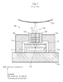
- an optical print head 700 that uses OLEDs forms an electrostatic latent image through condensing light emitted from the OLEDs 712 onto an outer circumferential surface of a photoreceptor drum 750 with use of a lens array 730 .
- the lens array 730 includes many rod lenses 731 integrated with use of resin 732 , and is held by a lens holder 720 .
- the lens holder 720 is fixed by a base holder 740 .
- a rotational axis 752 of the photoreceptor drum 750 is supported by photoreceptor positioning members 751 , and the lens holder 720 contacts the photoreceptor positioning members 751 .
- This structure defines a distance from the lens array 730 to the outer circumferential surface of the photoreceptor drum 750 .
- the OLED panel 710 includes a glass substrate 711 and a thin film transistor (TFT) circuit 713 that includes the OLEDs 712 and that is disposed on the glass substrate 711 .
- a light-emitting region on the glass substrate 711 is sealed by a sealing material 714 in order to protect the OLEDs 712 from external air.
- the sealing material 714 is positioned relative to the photoreceptor drum 750 .
- a driver integrated circuit (IC) 800 for switching on and off the OLEDs 712 is disposed outside the region sealed by the sealing material 714 . That is, the OLED panel 710 is supported at only one end, and in a region around the driver IC 800 , the OLED panel 710 is in contact with neither the lens holder 720 nor the base holder 740 .
- Temperature increase of the driver IC 800 occurring in accordance with optical writing operations may cause malfunction or the like. Accordingly, the driver IC 800 is cooled through heat dissipation. However, thermal expansion of the lens holder 720 and thermal expansion of the photoreceptor positioning members 751 caused by heat conducted through the lens holder 720 may occur in accordance with how heat is dissipated from the driver IC 800 .
- Such thermal expansion causes changes in positions of the components relative to each other and a reduction in condensing ratio of light emitted from the OLEDs 712 and condensed onto the outer circumferential surface of the photoreceptor drum 750 , and consequently causes image quality deterioration. Accordingly, it is desirable that heat from the driver IC 800 be dissipated to the base holder 740 .
- conventional technology describes disposing a thermally conductive member 903 between a high heat generating part 901 and a display device fixing frame 902 as illustrated in FIG. 9 (see Japanese Patent Application Publication No. 2006-032615).
- Application of such conventional technology would help heat from the driver IC 800 to be dissipated to the base holder 740 through disposing a thermally conductive member between the driver IC 800 and the base holder 740 .
- One possible measure for overcoming this problem is to provide a support portion for supporting the lens holder 720 at a surface of the glass substrate 711 behind a surface of the glass substrate 711 on which the driver IC 800 is disposed.
- the lens holder 720 is in contact with the photoreceptor positioning member 751 , heat of the driver IC 800 may be conducted through the support portion to the lens holder 720 and the photoreceptor positioning member 751 . Accordingly, it is not desirable to provide, on the glass substrate 711 , a support portion for supporting the lens holder 720 .
- the present disclosure has been achieved in view of the above problems, and an aim thereof is to provide an optical print head and an image forming device that help suppress displacement of OLEDs and conduction of heat from a driver IC to a lens holder.
- an optical print head reflecting at least one aspect of the present disclosure includes: an elongated light source substrate that has a line-shaped region in which a plurality of light-emitting elements are arranged; an optical member that condenses light emitted from the light-emitting elements onto an irradiation target; a holding member that holds the optical member; a base member that holds the light source substrate and the holding member; an integrated circuit that is mounted in a first region on a first surface of the light source substrate, the first surface facing the base member and the first region being in proximity of an end in a longitudinal direction of the light source substrate, heat being generated in the integrated circuit during optical writing; and a thermally conductive member that is disposed between the integrated circuit and the base member, wherein the holding member has a support portion contacting the light source substrate in a second region on a second surface of the light source substrate, the second surface not facing the base member and the second region being at a position differing from the first region in plan view
- FIG. 1 is a schematic diagram of main components of an image forming device pertaining to a first embodiment of the present disclosure
- FIG. 2 is a cross-sectional view of main components of an optical print head 100 ;
- FIG. 3 is a cross-sectional perspective view of one end of the optical print head 100 ;
- FIG. 4 is an external perspective view of a structure of a positioning member 250 ;
- FIG. 5A is a cross-sectional view of a shape of a support portion 222 pertaining to a modification of the present disclosure
- FIG. 5B is a cross-sectional perspective view of a shape of the support portion 222 pertaining to the modification of the present disclosure
- FIG. 6A is a cross-sectional view of a shape of a support portion 222 pertaining to a modification of the present disclosure
- FIG. 6B is a cross-sectional perspective view of a shape of the support portion 222 pertaining to the modification of the present disclosure
- FIG. 7 is a cross-sectional view of main components of an optical print head pertaining to conventional technology, taken along a cross-section orthogonal to a main scanning direction;
- FIG. 8 is a cross-sectional view of main components of the optical print head pertaining to conventional technology, taken along a cross-section orthogonal to a sub scanning direction;
- FIG. 9 is a cross-sectional view of how heat is dissipated from high heat generating parts pertaining to conventional technology.
- the following describes a structure of an image forming device pertaining to the present embodiment.
- an image forming device 1 is a so-called tandem-type color printer device, and includes image forming units 101 Y, 101 M, 101 C, and 101 K forming images of colors yellow (Y), magenta (M), cyan (C), and black (K), respectively.
- the image forming unit 101 Y includes an optical print head 100 Y, a photoreceptor drum 110 Y, an electricity charging device 111 Y, a developing device 112 Y, and a cleaning device 114 Y.
- the image forming unit 101 M includes an optical print head 100 M, a photoreceptor drum 110 M, an electricity charging device 111 M, a developing device 112 M, and a cleaning device 114 M;
- the image forming unit 101 C includes an optical print head 100 C, a photoreceptor drum 110 C, an electricity charging device 111 C, a developing device 112 C, and a cleaning device 114 C;
- the image forming unit 101 K includes an optical print head 100 K, a photoreceptor drum 110 K, an electricity charging device 111 K, a developing device 112 K, and a cleaning device 114 K.
- the image forming units 101 Y, 101 M, 101 C, and 101 K respectively cause outer circumferential surfaces of the photoreceptor drums 110 Y, 110 M, 110 C, and 110 K to be uniformly charged by the electricity charging devices 111 Y, 111 M, 111 C, and 111 K. Then the image forming units 101 Y, 101 M, 101 C, and 101 K respectively cause the optical print heads 100 Y, 100 M, 100 C, and 100 K to each form an electrostatic latent image, and respectively cause the developing devices 112 Y, 112 M, 112 C, and 112 K to develop the electrostatic latent images.
- Primary transfer rollers 113 Y, 113 M, 113 C, and 113 K electrostatically transfer the toner images of the colors Y, M, C, and K respectively carried on the outer circumferential surfaces of the photoreceptor drums 110 Y, 110 M, 110 C, and 110 K onto an intermediate transfer belt 102 in sequence, so that the toner images overlap each other. A color toner image is thus formed. Then, toner remaining on the outer circumferential surfaces of the photoreceptor drums 110 Y, 110 M, 110 C, and 110 K is removed by the cleaner devices 114 Y, 114 M, 114 C, and 114 K, respectively.
- the intermediate transfer belt 102 is an endless belt, and rotates in a direction indicated by arrow A in order to convey the color toner image to a second transfer roller pair 103 .
- a recording sheet S contained in a sheet feed tray 104 is picked up and conveyed to the secondary transfer roller pair 103 .
- the color toner image on the intermediate transfer belt 102 is electrostatically transferred onto the recording sheet S.
- the color toner image on the recording sheet S is thermally fixed by a fixing device 105 , and the recording sheet S is ejected onto a sheet ejection tray 106 .
- the following describes a structure of the optical print head 100 .
- the optical print head 100 includes an OLED panel 210 , a lens holder 220 , a lens array 230 , and a base holder 240 .
- the OLED panel 210 is a light emitting substrate elongated in a main scanning direction and has a thin film transistor (TFT) circuit 213 including a plurality of (for example, 15,000) organic light-emitting elements (OLEDs) 212 arranged in a line-shaped region on a glass substrate 211 .
- TFT thin film transistor
- a driver integrated circuit (IC) 215 is connected to the TFT circuit 213 , and during optical writing, the driver IC 215 turns on and off the OLEDs 212 in accordance with image data.
- the OLEDs 212 are arrayed in a line or a plurality of lines in a staggered pattern, and the light-emitting region including the OLEDs 212 is sealed by a sealing member 214 in order to protect the OLEDs 212 from dust.
- the sealing member 214 is in contact with a support portion 241 of the base holder 240 .
- the support portion 241 may be a semispherical protrusion or hardened adhesive.
- the sealing member 214 contacts the support portion 241 to position the OLED panel 210 .
- the base holder 240 is a member molded out of a sheet metal.
- the sheet metal material for the base holder 240 is a steel material such as stainless steel (SUS) having thermal conductivity Kh of approximately 20 W/m ⁇ K.
- the thermally conductive silicone member 260 may be silicone grease applied to the driver IC 215 and hardened, or may be a sheet-like silicone member sandwiched between the driver IC 215 and the base holder 240 .
- a region A from an end in a longitudinal direction of the glass substrate 211 to the driver IC 215 has a length Da that is shorter than a length Db of a region B from the sealing member 214 to the driver IC 215 . Because the glass substrate 211 has a constant width in a transverse direction irrespective of positions in the longitudinal direction, the region A has a smaller area than the region B.
- a glass material for the glass substrate 211 has thermal conductivity Kp of approximately 1.0 W/m ⁇ K.
- the lens array 230 includes a plurality of rod lenses 231 arranged in two or more rows in the main scanning direction in a staggered pattern and fixed by resin 232 .
- the lens array 230 condenses light P emitted from the OLEDs 212 onto the outer circumferential surface of the photoreceptor drum 110 .
- a SELFOC lens array SLA; SELFOC is a registered trademark of Nippon Sheet Glass Co. Ltd.
- the lens holder 220 includes resin and is fixed to the base holder 240 with the lens array 230 held by the lens holder 220 .
- the lens holder 220 has, in proximity of each end in a longitudinal direction of the lens holder 220 , a protrusion 221 .
- Each protrusion 221 has a semispherical tip that contacts a corresponding one of positioning members 250 of the photoreceptor drum 110 .
- This structure defines positions relative to each other of the outer circumferential surface of the photoreceptor drum 110 , the rod lenses 231 , and the OLEDs 212 .
- the resin material for the lens holder 220 has thermal conductivity Ks ranging from 0.4 W/m ⁇ K to 0.5 W/m ⁇ K.
- orienting resin obtained through adding a reinforcing agent such as glass fiber to a general-purpose engineering plastic can be used.
- resin that does not include glass fiber may be used.
- liquid crystal polymer resin, polycarbonate, synthetic resin of polycarbonate and acrylonitrile butadiene styrene (ABS) resin, synthetic resin of polycarbonate and polystyrene, or the like may be used.
- a positioning member 250 has an end surface 251 contacting a protrusion 221 .
- the photoreceptor drum 110 includes a flange portion 301 , a drum portion 302 , and a rotational axis 401 .
- the rotational axis 401 passes through the positioning member 250 .
- the positioning member 250 is screwed to the housing (not illustrated) of the image forming unit 101 at a middle portion 252 between a portion of the positioning member 250 through which the rotational axis 401 passes and the end surface 251 .
- the lens holder 220 has a support portion 222 .
- the support portion 222 contacts a main surface of the glass substrate 211 facing the lens array 230 . Further, the support portion 222 contacts the glass substrate 211 at a position in a longitudinal direction between the driver IC 215 and the support portion 241 of the base holder 240 .
- components such as cables for connecting the optical print head 100 and other portions of the image forming device 1 are not illustrated in FIG. 2 , FIG. 3 , or FIG. 4 .
- Grease silicone shrinks when hardened. Further, a silicone sheet shrinks in an optical axis direction (direction parallel to optical axes of the rod lenses 731 ) after being fitted to the driver IC 215 and the base holder 240 .
- the thermally conductive silicone member 260 shrinks, while the base holder 240 does not deform due to having high rigidity, the glass substrate 211 deflects due to having low rigidity.
- the driver IC 215 is attracted toward the base holder 240 .
- a light-emitting region of the glass substrate 211 where the OLEDs 212 are mounted deflects toward the base holder 240 .
- the reaction force causes the glass substrate 211 between the driver IC 215 and the light-emitting region of the glass substrate 211 to deflect toward the lens holder 220 .
- the support portion 222 of the lens holder 220 contacts the glass substrate 211 between the driver IC 215 and the light-emitting region of the glass substrate 211 .
- This structure helps prevent the glass substrate 211 from deflecting toward the lens holder 220 .
- the light-emitting region of the glass substrate 211 can be prevented from deflecting toward the base holder 240 .
- the support portion 222 of the lens holder 220 contacts the glass substrate 211 at a position in the longitudinal direction between the driver IC 215 and the support portion 241 of the base holder 240 . Accordingly, in order for heat from the driver IC 215 to be conducted to the lens holder 220 , the heat is conducted through the glass substrate 211 .
- the glass substrate 211 has low thermal conductivity due to including a glass material, which has low thermal conductivity, and due to having small thickness in the optical axis direction. Accordingly, less heat from the driver IC 215 is conducted to the lens holder 220 compared to structures in which the heat conduction path from the driver IC 215 to the lens holder 220 has a minimum length due to disposition of the support portion 241 at a position overlapping the driver IC 215 in plan view from the optical axis direction.
- heat from the driver IC 215 is dissipated through the thermally conductive silicone member 260 to the base holder 240 . This further helps reduce heat amount conducted from the driver IC 215 to the lens holder 220 .
- the structure pertaining to the present embodiment helps suppress heat amount conducted from the driver IC 215 to the lens holder 220 . This helps prevent a decrease in condensing ratio of light emitted from the OLEDs 212 caused by thermal deformation of the lens holder 220 and the positioning members 250 , and consequently helps prevent image quality deterioration.
- the positioning members 250 contact the base holder 240 incur high costs because sheet metal working is used in order to provide the base holder 240 with protrusions contacting the positioning members 250 .
- the lens holder 220 is formed through resin molding with use of a metal mold. That is, the protrusion is formed by simply using a metal mold designed for forming the lens holder 220 along with the protrusion 221 . This helps reduce costs because a process of working each instance of the lens holder 220 is not necessary.
- heat conducted from the driver IC 215 through the thermally conductive silicone member 260 to the base holder 240 may further be conducted to the positioning members 250 .
- This may cause image quality deterioration due to thermal deformation of the positioning members 250 .
- the present embodiment helps prevent such image quality deterioration.
- the glass substrate 211 has a smaller area in the region A than in the region B. Accordingly, the region B has greater thermal resistance, and thus suppresses heat increase to a greater extent than the region A. Accordingly, the structure of the present embodiment in which the support portion 222 contacts the region B has a greater effect of helping suppression of conduction of heat from the driver IC 215 to the lens holder 220 compared to structures in which the support portion 222 contacts the region A.
- the support portion 222 of the lens holder 220 contacts the OLED panel 210 at a position differing in the longitudinal direction from the position of the support portion 241 of the base holder 240 . Specifically, in the present embodiment, the support portion 222 contacts the glass substrate 211 at a position closer to the driver IC 215 than the support portion 241 . Such a structure helps suppress bending moment of the OLED panel 210 , and consequently helps prevent the OLEDs 212 from being displaced in the optical axis direction.
- a material having low thermal conductivity has great thermal resistance. Accordingly, a glass substrate 211 including a material having low thermal conductivity helps suppress conduction of heat from the driver IC 215 , which is disposed on the glass substrate 211 , through the glass substrate 211 to other components. This structure helps improve heat dissipation efficiency through helping heat from the driver IC 215 to be conducted through the thermally conductive silicone member 260 to the base holder 240 .
- thermal conductivity Ks of the resin material for the lens holder 220 is lower than thermal conductivity Kp of the glass material for the glass substrate 211 and lower than thermal conductivity Kh of the sheet metal material for the base holder 240 , conduction of heat to the lens holder 220 and conduction of heat through the lens holder 220 to the positioning members 250 can further be suppressed.
- the above embodiment takes a case in which a tip of the support portion 222 of the lens holder 220 is flat as an example.
- the present invention of course should not be construed as being limited to this, and may be configured as follows.
- the tip of the support portion 222 is notched, and consequently has a large surface area as in FIG. 5A and FIG. 5B , the support portion 222 has great heat dissipating property. This consequently helps suppress conduction of heat from the driver IC 215 through the glass substrate 211 and the support portion 222 to a main body of the lens holder 220 and the positioning members 250 .
- the notches at the tip of the support portion 222 may be grooves or a plurality of protrusions.
- the tip of the support portion 222 may be rounded as in FIG. 6A and FIG. 6B .
- contacting area between the glass substrate 211 and the lens holder 220 is small, and this helps suppress conduction of heat from the driver IC 215 to the lens holder 220 and the positioning members 250 .
- the base holder 240 has the support portion 241 as an example.
- the present invention of course should not be construed as being limited to this, and may be configured as follows.
- the support portion 222 of the lens holder 220 may contact the glass substrate 211 at a position in the longitudinal direction between the driver IC 215 and a position at which the sealing member 214 is fixed to the base holder 240 .
- the effects of the present invention can be achieved in structures in which the support portion 222 contacts the glass substrate 211 of the OLED panel 215 at a position in the longitudinal direction between the driver IC 215 and the position of the base holder 240 at which the base holder 240 contacts the OLED panel 210 , irrespective of how the OLED panel 210 is fixed to the base holder 240 .
- the support portion 222 of the lens holder 220 contacts the glass substrate 211 of the OLED panel 210 .
- the support portion 222 may be provided in different manners as long as the tip of the support portion 222 is at a position at which deflection of the glass substrate 211 caused by the thermally conductive silicone member 260 can be suppressed. Accordingly, the support portion 222 may not necessarily be in contact with the glass substrate 211 when deflection of the glass substrate 211 is small and does not affect image quality.
- the image forming device 1 is a tandem-type color printer as an example.
- the present invention of course should not be construed as being limited to this, and the image forming device 1 may be a color printer device of a type other than a tandem type or may be a monochrome printer.
- the present invention achieves similar effects when applied to single-function peripherals such as copiers including a scanner device, facsimile devices having a facsimile communication function, and multi-function peripherals (MFPs) including all such functions.
- MFPs multi-function peripherals
- an optical print head reflecting at least one aspect of the present disclosure includes: an elongated light source substrate that has a line-shaped region in which a plurality of light-emitting elements are arranged; an optical member that condenses light emitted from the light-emitting elements onto an irradiation target; a holding member that holds the optical member; a base member that holds the light source substrate and the holding member; an integrated circuit that is mounted in a first region on a first surface of the light source substrate, the first surface facing the base member and the first region being in proximity of an end in a longitudinal direction of the light source substrate, heat being generated in the integrated circuit during optical writing; and a thermally conductive member that is disposed between the integrated circuit and the base member, wherein the holding member has a support portion contacting the light source substrate in a second region on a second surface of the light source substrate, the second surface not facing the base member and the second region being at a position differing from the first region in plan view.
- the support portion of the holding member contacts the light source substrate in a second region on the second surface of the light source substrate at a position differing from the first region in plan view, where the second surface does not face the base member and the first region is a region in which the integrated circuit is mounted on the first surface of the light source substrate.
- the holding member may be in contact with a positioning member defining a distance from the optical member to the irradiation target.
- the support portion may contact the light source substrate at a position that is offset from a straight line extending from the position at which the positioning member contacts the holding member to the integrated circuit in plan view.
- the support portion may contact the light source substrate at a position in the longitudinal direction of the light source substrate between the integrated circuit and the light-emitting elements.
- the support portion may contact the light source substrate at a position in the longitudinal direction of the light source substrate between the integrated circuit and a position at which the base member contacts the light source substrate.
- the light source substrate may include a substrate on which the plurality of light-emitting elements are mounted, a material for the base member may have greater thermal conductivity than a material for the substrate, and the material for the substrate may have greater thermal conductivity than a material for the holding member.
- the support portion may protrude from a main body of the holding member toward the light source substrate, and a tip of the support portion contacting the light source substrate may be notched.
- the support portion may protrude from a main body of the holding member toward the light source substrate, and a tip of the support portion contacting the light source substrate may be rounded toward the light source substrate.
- the light-emitting elements may be organic light-emitting diodes.
- An image forming device reflecting at least one aspect of the present disclosure includes an optical print head, including: an elongated light source substrate that has a line-shaped region in which a plurality of light-emitting elements are arranged; an optical member that condenses light emitted from the light-emitting elements onto an irradiation target; a holding member that holds the optical member; a base member that holds the light source substrate and the holding member; an integrated circuit that is mounted in a first region on a first surface of the light source substrate, the first surface facing the base member and the first region being in proximity of an end in a longitudinal direction of the light source substrate, heat being generated in the integrated circuit during optical writing; and a thermally conductive member that is disposed between the integrated circuit and the base member, wherein the holding member has a support portion contacting the light source substrate in a second region on a second surface of the light source substrate, the second surface not facing the base member and the second region being at a position differing from the first region in plan view.
Landscapes
- Physics & Mathematics (AREA)
- Health & Medical Sciences (AREA)
- General Health & Medical Sciences (AREA)
- Toxicology (AREA)
- Optics & Photonics (AREA)
- Engineering & Computer Science (AREA)
- Multimedia (AREA)
- Signal Processing (AREA)
- General Physics & Mathematics (AREA)
- Printers Or Recording Devices Using Electromagnetic And Radiation Means (AREA)
- Electroluminescent Light Sources (AREA)
- Facsimile Heads (AREA)
- Exposure Or Original Feeding In Electrophotography (AREA)
Abstract
Description
Claims (10)
Applications Claiming Priority (2)
| Application Number | Priority Date | Filing Date | Title |
|---|---|---|---|
| JP2017-038184 | 2017-03-01 | ||
| JP2017038184A JP2018144246A (en) | 2017-03-01 | 2017-03-01 | Optical writing device and image formation apparatus |
Publications (2)
| Publication Number | Publication Date |
|---|---|
| US20180250952A1 US20180250952A1 (en) | 2018-09-06 |
| US10434794B2 true US10434794B2 (en) | 2019-10-08 |
Family
ID=63357185
Family Applications (1)
| Application Number | Title | Priority Date | Filing Date |
|---|---|---|---|
| US15/902,644 Expired - Fee Related US10434794B2 (en) | 2017-03-01 | 2018-02-22 | Optical print head and image forming device |
Country Status (3)
| Country | Link |
|---|---|
| US (1) | US10434794B2 (en) |
| JP (1) | JP2018144246A (en) |
| CN (1) | CN108535977B (en) |
Citations (5)
| Publication number | Priority date | Publication date | Assignee | Title |
|---|---|---|---|---|
| JP2006032615A (en) | 2004-07-15 | 2006-02-02 | Nec Infrontia Corp | Electronic apparatus |
| JP2011245775A (en) | 2010-05-28 | 2011-12-08 | Ricoh Co Ltd | Light source device, and image forming apparatus |
| US20160268179A1 (en) * | 2015-03-11 | 2016-09-15 | Kabushiki Kaisha Toshiba | Semiconductor device and electronic device |
| US20170080700A1 (en) * | 2015-05-27 | 2017-03-23 | Landa Labs (2012) Ltd. | Printing Method and Apparatus for Coating Selected Regions of a Substrate with a Film |
| US20170115592A1 (en) * | 2015-10-27 | 2017-04-27 | Konica Minolta, Inc. | Light emitting device, optical write-in device, and image forming device |
Family Cites Families (7)
| Publication number | Priority date | Publication date | Assignee | Title |
|---|---|---|---|---|
| JP2007237575A (en) * | 2006-03-09 | 2007-09-20 | Seiko Epson Corp | Electro-optical device, image forming apparatus, and electro-optical device manufacturing method |
| JP2007237637A (en) * | 2006-03-10 | 2007-09-20 | Seiko Epson Corp | Electro-optical device and image forming apparatus |
| JP2007253502A (en) * | 2006-03-24 | 2007-10-04 | Seiko Epson Corp | Electro-optical device, image forming apparatus, and electro-optical device manufacturing method |
| CN101491977A (en) * | 2008-01-21 | 2009-07-29 | 精工爱普生株式会社 | Line head and image forming apparatus using the same |
| US20110242252A1 (en) * | 2010-04-01 | 2011-10-06 | Kabushiki Kaisha Toshiba | Optical head and image forming apparatus |
| JP6123702B2 (en) * | 2014-02-24 | 2017-05-10 | コニカミノルタ株式会社 | Optical writing apparatus and image forming apparatus |
| JP6447052B2 (en) * | 2014-11-25 | 2019-01-09 | コニカミノルタ株式会社 | Optical writing apparatus and image forming apparatus |
-
2017
- 2017-03-01 JP JP2017038184A patent/JP2018144246A/en active Pending
-
2018
- 2018-02-22 US US15/902,644 patent/US10434794B2/en not_active Expired - Fee Related
- 2018-02-28 CN CN201810166968.XA patent/CN108535977B/en active Active
Patent Citations (5)
| Publication number | Priority date | Publication date | Assignee | Title |
|---|---|---|---|---|
| JP2006032615A (en) | 2004-07-15 | 2006-02-02 | Nec Infrontia Corp | Electronic apparatus |
| JP2011245775A (en) | 2010-05-28 | 2011-12-08 | Ricoh Co Ltd | Light source device, and image forming apparatus |
| US20160268179A1 (en) * | 2015-03-11 | 2016-09-15 | Kabushiki Kaisha Toshiba | Semiconductor device and electronic device |
| US20170080700A1 (en) * | 2015-05-27 | 2017-03-23 | Landa Labs (2012) Ltd. | Printing Method and Apparatus for Coating Selected Regions of a Substrate with a Film |
| US20170115592A1 (en) * | 2015-10-27 | 2017-04-27 | Konica Minolta, Inc. | Light emitting device, optical write-in device, and image forming device |
Also Published As
| Publication number | Publication date |
|---|---|
| CN108535977A (en) | 2018-09-14 |
| JP2018144246A (en) | 2018-09-20 |
| CN108535977B (en) | 2021-03-23 |
| US20180250952A1 (en) | 2018-09-06 |
Similar Documents
| Publication | Publication Date | Title |
|---|---|---|
| US7760224B2 (en) | Exposure device and image forming apparatus with supporting member for focusing lens and light emitting element array | |
| CN110361947B (en) | Optical writing device and image forming apparatus | |
| US20160219177A1 (en) | Optical scanning apparatus and image forming apparatus | |
| US10434794B2 (en) | Optical print head and image forming device | |
| US11347158B2 (en) | Image forming apparatus including optical print head | |
| JP4736433B2 (en) | LIGHT EMITTING DEVICE, MANUFACTURING METHOD THEREOF, IMAGE FORMING DEVICE, AND IMAGE READING DEVICE | |
| US8416497B2 (en) | Lens array unit, optical head and information apparatus | |
| JP6365019B2 (en) | Optical writing apparatus and image forming apparatus | |
| JP6862808B2 (en) | Optical writing device and image forming device | |
| US7942547B2 (en) | Light emitting device and electronic apparatus | |
| JP6816473B2 (en) | Optical writing device and image forming device | |
| US12298679B2 (en) | Print head | |
| US20200117113A1 (en) | Print head and image forming apparatus which includes print head | |
| US10281875B2 (en) | Optical scanning device and image forming device having the same | |
| JP6672930B2 (en) | Optical writing device, image forming apparatus, and method of holding rod lens unit | |
| US20200133193A1 (en) | Image forming apparatus including optical print head | |
| JP4552665B2 (en) | LIGHT EMITTING DEVICE, MANUFACTURING METHOD THEREOF, IMAGE FORMING DEVICE, AND IMAGE READING DEVICE | |
| US20250370406A1 (en) | Exposure device and image forming apparatus | |
| US20250370403A1 (en) | Image forming apparatus | |
| JP2009255519A (en) | Exposure head and image forming device | |
| US20250021032A1 (en) | Exposure device and image forming apparatus | |
| CN102243370A (en) | Optical scanning device and image forming apparatus | |
| JP2008080759A (en) | Printer head | |
| JP2019135525A (en) | Optical writer and image forming apparatus including the same | |
| JP2025181089A (en) | Exposure device and image forming device |
Legal Events
| Date | Code | Title | Description |
|---|---|---|---|
| AS | Assignment |
Owner name: KONICA MINOLTA, INC., JAPAN Free format text: ASSIGNMENT OF ASSIGNORS INTEREST;ASSIGNORS:YUASA, TAKAFUMI;TANIYAMA, AKIRA;TACHIBE, HIDENARI;REEL/FRAME:045417/0280 Effective date: 20180129 |
|
| FEPP | Fee payment procedure |
Free format text: ENTITY STATUS SET TO UNDISCOUNTED (ORIGINAL EVENT CODE: BIG.); ENTITY STATUS OF PATENT OWNER: LARGE ENTITY |
|
| STPP | Information on status: patent application and granting procedure in general |
Free format text: DOCKETED NEW CASE - READY FOR EXAMINATION |
|
| STPP | Information on status: patent application and granting procedure in general |
Free format text: NOTICE OF ALLOWANCE MAILED -- APPLICATION RECEIVED IN OFFICE OF PUBLICATIONS |
|
| STPP | Information on status: patent application and granting procedure in general |
Free format text: PUBLICATIONS -- ISSUE FEE PAYMENT VERIFIED |
|
| STCF | Information on status: patent grant |
Free format text: PATENTED CASE |
|
| FEPP | Fee payment procedure |
Free format text: MAINTENANCE FEE REMINDER MAILED (ORIGINAL EVENT CODE: REM.); ENTITY STATUS OF PATENT OWNER: LARGE ENTITY |
|
| LAPS | Lapse for failure to pay maintenance fees |
Free format text: PATENT EXPIRED FOR FAILURE TO PAY MAINTENANCE FEES (ORIGINAL EVENT CODE: EXP.); ENTITY STATUS OF PATENT OWNER: LARGE ENTITY |
|
| STCH | Information on status: patent discontinuation |
Free format text: PATENT EXPIRED DUE TO NONPAYMENT OF MAINTENANCE FEES UNDER 37 CFR 1.362 |
|
| FP | Lapsed due to failure to pay maintenance fee |
Effective date: 20231008 |