US10429691B2 - Regional polarization structure, method for fabricating regional polarization structure and liquid crystal display panel - Google Patents
Regional polarization structure, method for fabricating regional polarization structure and liquid crystal display panel Download PDFInfo
- Publication number
- US10429691B2 US10429691B2 US14/984,889 US201514984889A US10429691B2 US 10429691 B2 US10429691 B2 US 10429691B2 US 201514984889 A US201514984889 A US 201514984889A US 10429691 B2 US10429691 B2 US 10429691B2
- Authority
- US
- United States
- Prior art keywords
- carbon nanotube
- substrate
- nanotube block
- polarization structure
- liquid crystal
- Prior art date
- Legal status (The legal status is an assumption and is not a legal conclusion. Google has not performed a legal analysis and makes no representation as to the accuracy of the status listed.)
- Active, expires
Links
- 230000010287 polarization Effects 0.000 title claims abstract description 85
- 239000004973 liquid crystal related substance Substances 0.000 title claims abstract description 58
- 238000000034 method Methods 0.000 title abstract description 27
- OKTJSMMVPCPJKN-UHFFFAOYSA-N Carbon Chemical compound [C] OKTJSMMVPCPJKN-UHFFFAOYSA-N 0.000 claims abstract description 188
- 239000002041 carbon nanotube Substances 0.000 claims abstract description 184
- 229910021393 carbon nanotube Inorganic materials 0.000 claims abstract description 184
- 239000000758 substrate Substances 0.000 claims abstract description 119
- 239000000463 material Substances 0.000 claims description 36
- 238000009413 insulation Methods 0.000 claims description 12
- 238000005411 Van der Waals force Methods 0.000 claims description 10
- VYPSYNLAJGMNEJ-UHFFFAOYSA-N Silicium dioxide Chemical group O=[Si]=O VYPSYNLAJGMNEJ-UHFFFAOYSA-N 0.000 claims description 6
- 235000012239 silicon dioxide Nutrition 0.000 claims description 3
- 239000000377 silicon dioxide Substances 0.000 claims description 3
- 239000002238 carbon nanotube film Substances 0.000 description 36
- 238000010586 diagram Methods 0.000 description 6
- 238000005530 etching Methods 0.000 description 4
- 230000002708 enhancing effect Effects 0.000 description 1
- 239000002071 nanotube Substances 0.000 description 1
- 230000000750 progressive effect Effects 0.000 description 1
- 230000005855 radiation Effects 0.000 description 1
Images


Classifications
-
- G—PHYSICS
- G02—OPTICS
- G02F—OPTICAL DEVICES OR ARRANGEMENTS FOR THE CONTROL OF LIGHT BY MODIFICATION OF THE OPTICAL PROPERTIES OF THE MEDIA OF THE ELEMENTS INVOLVED THEREIN; NON-LINEAR OPTICS; FREQUENCY-CHANGING OF LIGHT; OPTICAL LOGIC ELEMENTS; OPTICAL ANALOGUE/DIGITAL CONVERTERS
- G02F1/00—Devices or arrangements for the control of the intensity, colour, phase, polarisation or direction of light arriving from an independent light source, e.g. switching, gating or modulating; Non-linear optics
- G02F1/01—Devices or arrangements for the control of the intensity, colour, phase, polarisation or direction of light arriving from an independent light source, e.g. switching, gating or modulating; Non-linear optics for the control of the intensity, phase, polarisation or colour
- G02F1/13—Devices or arrangements for the control of the intensity, colour, phase, polarisation or direction of light arriving from an independent light source, e.g. switching, gating or modulating; Non-linear optics for the control of the intensity, phase, polarisation or colour based on liquid crystals, e.g. single liquid crystal display cells
- G02F1/133—Constructional arrangements; Operation of liquid crystal cells; Circuit arrangements
- G02F1/1333—Constructional arrangements; Manufacturing methods
- G02F1/1335—Structural association of cells with optical devices, e.g. polarisers or reflectors
- G02F1/133528—Polarisers
-
- G—PHYSICS
- G02—OPTICS
- G02F—OPTICAL DEVICES OR ARRANGEMENTS FOR THE CONTROL OF LIGHT BY MODIFICATION OF THE OPTICAL PROPERTIES OF THE MEDIA OF THE ELEMENTS INVOLVED THEREIN; NON-LINEAR OPTICS; FREQUENCY-CHANGING OF LIGHT; OPTICAL LOGIC ELEMENTS; OPTICAL ANALOGUE/DIGITAL CONVERTERS
- G02F1/00—Devices or arrangements for the control of the intensity, colour, phase, polarisation or direction of light arriving from an independent light source, e.g. switching, gating or modulating; Non-linear optics
- G02F1/01—Devices or arrangements for the control of the intensity, colour, phase, polarisation or direction of light arriving from an independent light source, e.g. switching, gating or modulating; Non-linear optics for the control of the intensity, phase, polarisation or colour
- G02F1/13—Devices or arrangements for the control of the intensity, colour, phase, polarisation or direction of light arriving from an independent light source, e.g. switching, gating or modulating; Non-linear optics for the control of the intensity, phase, polarisation or colour based on liquid crystals, e.g. single liquid crystal display cells
- G02F1/133—Constructional arrangements; Operation of liquid crystal cells; Circuit arrangements
- G02F1/1333—Constructional arrangements; Manufacturing methods
- G02F1/1337—Surface-induced orientation of the liquid crystal molecules, e.g. by alignment layers
- G02F1/133753—Surface-induced orientation of the liquid crystal molecules, e.g. by alignment layers with different alignment orientations or pretilt angles on a same surface, e.g. for grey scale or improved viewing angle
-
- G—PHYSICS
- G02—OPTICS
- G02B—OPTICAL ELEMENTS, SYSTEMS OR APPARATUS
- G02B1/00—Optical elements characterised by the material of which they are made; Optical coatings for optical elements
- G02B1/04—Optical elements characterised by the material of which they are made; Optical coatings for optical elements made of organic materials, e.g. plastics
-
- G—PHYSICS
- G02—OPTICS
- G02B—OPTICAL ELEMENTS, SYSTEMS OR APPARATUS
- G02B5/00—Optical elements other than lenses
- G02B5/30—Polarising elements
- G02B5/3016—Polarising elements involving passive liquid crystal elements
-
- G—PHYSICS
- G02—OPTICS
- G02F—OPTICAL DEVICES OR ARRANGEMENTS FOR THE CONTROL OF LIGHT BY MODIFICATION OF THE OPTICAL PROPERTIES OF THE MEDIA OF THE ELEMENTS INVOLVED THEREIN; NON-LINEAR OPTICS; FREQUENCY-CHANGING OF LIGHT; OPTICAL LOGIC ELEMENTS; OPTICAL ANALOGUE/DIGITAL CONVERTERS
- G02F1/00—Devices or arrangements for the control of the intensity, colour, phase, polarisation or direction of light arriving from an independent light source, e.g. switching, gating or modulating; Non-linear optics
- G02F1/01—Devices or arrangements for the control of the intensity, colour, phase, polarisation or direction of light arriving from an independent light source, e.g. switching, gating or modulating; Non-linear optics for the control of the intensity, phase, polarisation or colour
- G02F1/13—Devices or arrangements for the control of the intensity, colour, phase, polarisation or direction of light arriving from an independent light source, e.g. switching, gating or modulating; Non-linear optics for the control of the intensity, phase, polarisation or colour based on liquid crystals, e.g. single liquid crystal display cells
- G02F1/133—Constructional arrangements; Operation of liquid crystal cells; Circuit arrangements
- G02F1/1333—Constructional arrangements; Manufacturing methods
- G02F1/1337—Surface-induced orientation of the liquid crystal molecules, e.g. by alignment layers
- G02F1/133707—Structures for producing distorted electric fields, e.g. bumps, protrusions, recesses, slits in pixel electrodes
-
- G—PHYSICS
- G02—OPTICS
- G02F—OPTICAL DEVICES OR ARRANGEMENTS FOR THE CONTROL OF LIGHT BY MODIFICATION OF THE OPTICAL PROPERTIES OF THE MEDIA OF THE ELEMENTS INVOLVED THEREIN; NON-LINEAR OPTICS; FREQUENCY-CHANGING OF LIGHT; OPTICAL LOGIC ELEMENTS; OPTICAL ANALOGUE/DIGITAL CONVERTERS
- G02F1/00—Devices or arrangements for the control of the intensity, colour, phase, polarisation or direction of light arriving from an independent light source, e.g. switching, gating or modulating; Non-linear optics
- G02F1/01—Devices or arrangements for the control of the intensity, colour, phase, polarisation or direction of light arriving from an independent light source, e.g. switching, gating or modulating; Non-linear optics for the control of the intensity, phase, polarisation or colour
- G02F1/13—Devices or arrangements for the control of the intensity, colour, phase, polarisation or direction of light arriving from an independent light source, e.g. switching, gating or modulating; Non-linear optics for the control of the intensity, phase, polarisation or colour based on liquid crystals, e.g. single liquid crystal display cells
- G02F1/133—Constructional arrangements; Operation of liquid crystal cells; Circuit arrangements
- G02F1/1333—Constructional arrangements; Manufacturing methods
- G02F1/1337—Surface-induced orientation of the liquid crystal molecules, e.g. by alignment layers
- G02F1/13378—Surface-induced orientation of the liquid crystal molecules, e.g. by alignment layers by treatment of the surface, e.g. embossing, rubbing or light irradiation
-
- B—PERFORMING OPERATIONS; TRANSPORTING
- B82—NANOTECHNOLOGY
- B82Y—SPECIFIC USES OR APPLICATIONS OF NANOSTRUCTURES; MEASUREMENT OR ANALYSIS OF NANOSTRUCTURES; MANUFACTURE OR TREATMENT OF NANOSTRUCTURES
- B82Y20/00—Nanooptics, e.g. quantum optics or photonic crystals
-
- C—CHEMISTRY; METALLURGY
- C09—DYES; PAINTS; POLISHES; NATURAL RESINS; ADHESIVES; COMPOSITIONS NOT OTHERWISE PROVIDED FOR; APPLICATIONS OF MATERIALS NOT OTHERWISE PROVIDED FOR
- C09K—MATERIALS FOR MISCELLANEOUS APPLICATIONS, NOT PROVIDED FOR ELSEWHERE
- C09K2323/00—Functional layers of liquid crystal optical display excluding electroactive liquid crystal layer characterised by chemical composition
- C09K2323/02—Alignment layer characterised by chemical composition
-
- C—CHEMISTRY; METALLURGY
- C09—DYES; PAINTS; POLISHES; NATURAL RESINS; ADHESIVES; COMPOSITIONS NOT OTHERWISE PROVIDED FOR; APPLICATIONS OF MATERIALS NOT OTHERWISE PROVIDED FOR
- C09K—MATERIALS FOR MISCELLANEOUS APPLICATIONS, NOT PROVIDED FOR ELSEWHERE
- C09K2323/00—Functional layers of liquid crystal optical display excluding electroactive liquid crystal layer characterised by chemical composition
- C09K2323/03—Viewing layer characterised by chemical composition
-
- G—PHYSICS
- G02—OPTICS
- G02F—OPTICAL DEVICES OR ARRANGEMENTS FOR THE CONTROL OF LIGHT BY MODIFICATION OF THE OPTICAL PROPERTIES OF THE MEDIA OF THE ELEMENTS INVOLVED THEREIN; NON-LINEAR OPTICS; FREQUENCY-CHANGING OF LIGHT; OPTICAL LOGIC ELEMENTS; OPTICAL ANALOGUE/DIGITAL CONVERTERS
- G02F1/00—Devices or arrangements for the control of the intensity, colour, phase, polarisation or direction of light arriving from an independent light source, e.g. switching, gating or modulating; Non-linear optics
- G02F1/01—Devices or arrangements for the control of the intensity, colour, phase, polarisation or direction of light arriving from an independent light source, e.g. switching, gating or modulating; Non-linear optics for the control of the intensity, phase, polarisation or colour
- G02F1/13—Devices or arrangements for the control of the intensity, colour, phase, polarisation or direction of light arriving from an independent light source, e.g. switching, gating or modulating; Non-linear optics for the control of the intensity, phase, polarisation or colour based on liquid crystals, e.g. single liquid crystal display cells
- G02F1/133—Constructional arrangements; Operation of liquid crystal cells; Circuit arrangements
- G02F1/1333—Constructional arrangements; Manufacturing methods
- G02F1/1335—Structural association of cells with optical devices, e.g. polarisers or reflectors
- G02F1/133528—Polarisers
- G02F1/133538—Polarisers with spatial distribution of the polarisation direction
-
- G—PHYSICS
- G02—OPTICS
- G02F—OPTICAL DEVICES OR ARRANGEMENTS FOR THE CONTROL OF LIGHT BY MODIFICATION OF THE OPTICAL PROPERTIES OF THE MEDIA OF THE ELEMENTS INVOLVED THEREIN; NON-LINEAR OPTICS; FREQUENCY-CHANGING OF LIGHT; OPTICAL LOGIC ELEMENTS; OPTICAL ANALOGUE/DIGITAL CONVERTERS
- G02F1/00—Devices or arrangements for the control of the intensity, colour, phase, polarisation or direction of light arriving from an independent light source, e.g. switching, gating or modulating; Non-linear optics
- G02F1/01—Devices or arrangements for the control of the intensity, colour, phase, polarisation or direction of light arriving from an independent light source, e.g. switching, gating or modulating; Non-linear optics for the control of the intensity, phase, polarisation or colour
- G02F1/13—Devices or arrangements for the control of the intensity, colour, phase, polarisation or direction of light arriving from an independent light source, e.g. switching, gating or modulating; Non-linear optics for the control of the intensity, phase, polarisation or colour based on liquid crystals, e.g. single liquid crystal display cells
- G02F1/133—Constructional arrangements; Operation of liquid crystal cells; Circuit arrangements
- G02F1/1333—Constructional arrangements; Manufacturing methods
- G02F1/1337—Surface-induced orientation of the liquid crystal molecules, e.g. by alignment layers
- G02F1/133753—Surface-induced orientation of the liquid crystal molecules, e.g. by alignment layers with different alignment orientations or pretilt angles on a same surface, e.g. for grey scale or improved viewing angle
- G02F1/133757—Surface-induced orientation of the liquid crystal molecules, e.g. by alignment layers with different alignment orientations or pretilt angles on a same surface, e.g. for grey scale or improved viewing angle with different alignment orientations
-
- G—PHYSICS
- G02—OPTICS
- G02F—OPTICAL DEVICES OR ARRANGEMENTS FOR THE CONTROL OF LIGHT BY MODIFICATION OF THE OPTICAL PROPERTIES OF THE MEDIA OF THE ELEMENTS INVOLVED THEREIN; NON-LINEAR OPTICS; FREQUENCY-CHANGING OF LIGHT; OPTICAL LOGIC ELEMENTS; OPTICAL ANALOGUE/DIGITAL CONVERTERS
- G02F1/00—Devices or arrangements for the control of the intensity, colour, phase, polarisation or direction of light arriving from an independent light source, e.g. switching, gating or modulating; Non-linear optics
- G02F1/01—Devices or arrangements for the control of the intensity, colour, phase, polarisation or direction of light arriving from an independent light source, e.g. switching, gating or modulating; Non-linear optics for the control of the intensity, phase, polarisation or colour
- G02F1/13—Devices or arrangements for the control of the intensity, colour, phase, polarisation or direction of light arriving from an independent light source, e.g. switching, gating or modulating; Non-linear optics for the control of the intensity, phase, polarisation or colour based on liquid crystals, e.g. single liquid crystal display cells
- G02F1/133—Constructional arrangements; Operation of liquid crystal cells; Circuit arrangements
- G02F1/1333—Constructional arrangements; Manufacturing methods
- G02F1/1337—Surface-induced orientation of the liquid crystal molecules, e.g. by alignment layers
- G02F1/13378—Surface-induced orientation of the liquid crystal molecules, e.g. by alignment layers by treatment of the surface, e.g. embossing, rubbing or light irradiation
- G02F1/133792—Surface-induced orientation of the liquid crystal molecules, e.g. by alignment layers by treatment of the surface, e.g. embossing, rubbing or light irradiation by etching
-
- G02F2001/133538—
-
- G—PHYSICS
- G02—OPTICS
- G02F—OPTICAL DEVICES OR ARRANGEMENTS FOR THE CONTROL OF LIGHT BY MODIFICATION OF THE OPTICAL PROPERTIES OF THE MEDIA OF THE ELEMENTS INVOLVED THEREIN; NON-LINEAR OPTICS; FREQUENCY-CHANGING OF LIGHT; OPTICAL LOGIC ELEMENTS; OPTICAL ANALOGUE/DIGITAL CONVERTERS
- G02F2202/00—Materials and properties
- G02F2202/36—Micro- or nanomaterials
-
- Y10T428/10—
-
- Y10T428/1005—
-
- Y10T428/1036—
Definitions
- the present disclosure relates to the technical field of the liquid crystal display, and in particular to a regional polarization structure, a method for fabricating a regional polarization structure and a liquid crystal display panel including the regional polarization structure.
- a liquid crystal display panel has advantages of being ultra-thin, great size screen display, low power consumption, no radiation and high resolution. These features apply to current mainstream display devices and widely applied to various types of electronic devices.
- the liquid crystal display panel according to known technology includes: a TFT array substrate 11 and a color filter substrate 12 disposed oppositely; and a liquid crystal layer 13 disposed between the TFT array substrate 11 and the color filter substrate 12 .
- an alignment layer needs to be provided on a side of the TFT array substrate 11 facing the liquid crystal layer, such that liquid crystal molecules M have an initial deflection angle.
- the alignment layer of the existing liquid crystal display panel provides a uniform alignment direction at various positions, hence it is difficult to meet the requirement of different alignments at different positions of the liquid crystal display panel, thereby preventing the liquid crystal display panel from improving a display quality.
- a regional polarization structure, a method for fabricating a regional polarization structure and a liquid crystal display panel including the regional polarization structure are provided according to embodiments of the present disclosure, thereby solving the problem that the alignment layer of the existing liquid crystal display panel has a uniform alignment direction at various positions.
- the alignment layer of the existing liquid crystal display panel has a uniform alignment direction at various positions.
- a regional polarization structure which includes:
- At least one first carbon nanotube block arranged on a first side of the substrate, where the first carbon nanotube block includes multiple carbon nanotubes extended in a first direction;
- At least one second carbon nanotube block arranged on a second side of the substrate, where the second carbon nanotube block includes multiple carbon nanotubes extended in a second direction, and the second side is a side of the substrate opposite to the first side,
- a liquid crystal display panel which includes at least one regional polarization structure described above.
- a method for fabricating a regional polarization structure is provided, which is applied to the regional polarization structure described above.
- the method includes:
- first carbon nanotube film etching the first carbon nanotube film to form at least one first carbon nanotube block, where the first carbon nanotube block includes multiple carbon nanotubes extended in a first direction;
- a method for fabricating a regional polarization structure is provided, which is applied to the regional polarization structure described above, and the method includes:
- first carbon nanotube film etching the first carbon nanotube film to form at least one first carbon nanotube block, where the first carbon nanotube block includes multiple carbon nanotubes extended in a first direction;
- the regional polarization structure includes: a substrate; at least one first carbon nanotube block arranged on a first side of the substrate; and at least one second carbon nanotube block arranged on a second side of the substrate, where the first carbon nanotube block includes multiple carbon nanotubes extended in a first direction, the second carbon nanotube block includes multiple carbon nanotubes extended in a second direction, and the first direction is different from the second direction, i.e., the first carbon nanotube block and the second carbon nanotube block have different alignment directions.
- the regional polarization structure has different alignments at different regions according to the embodiments of the present disclosure, and thereby a liquid crystal display panel including the regional polarization structure has different alignments at different regions, so as to meet the requirement of different alignments at different positions of the liquid crystal display panel, and improve display quality due to the same alignment direction at different positions of the alignment layer.
- FIG. 1 is a schematic structural diagram of a liquid crystal display panel according to the conventional technology
- FIG. 2 is a top view of a regional polarization structure according to an embodiment of the present disclosure
- FIG. 3 is a partial cross section view of a regional polarization structure according to an embodiment of the present disclosure
- FIG. 4 is a partial cross section view of a regional polarization structure according to another embodiment of the present disclosure.
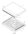
- FIG. 5 is a schematic structural diagram of a first carbon nanotube block in a regional polarization structure according to an embodiment of the present disclosure
- FIG. 6 is a cross section view of the first carbon nanotube block shown in FIG. 5 ;
- FIG. 7 is a schematic structural diagram of the carbon nanotube shown in FIG. 6 under a microscope
- FIG. 8 is a schematic partial structural diagram of a liquid crystal display panel according to an embodiment of the present disclosure.
- FIG. 9 is a schematic partial structural diagram of a liquid crystal display panel according to an embodiment of the present disclosure.
- FIG. 10 is a schematic partial structural diagram of a liquid crystal display panel according to an embodiment of the present disclosure.
- FIG. 11 is a flowchart of a method for fabricating a regional polarization structure according to an embodiment of the present disclosure
- FIG. 12 is a flowchart of a method for fabricating a regional polarization structure according to another embodiment of the present disclosure.
- FIG. 13 is a flowchart of a method for fabricating a regional polarization structure according to still another embodiment of the present disclosure.
- the regional polarization structure includes: a substrate 20 ; at least one first carbon nanotube block 21 arranged on a first side of the substrate 20 , where the first carbon nanotube block 21 includes multiple carbon nanotubes 24 extended in a first direction X, as shown in FIG. 5 and FIG. 6 ; and at least one second carbon nanotube block 22 arranged on a second side of the substrate 20 , where the second carbon nanotube block 22 includes multiple carbon nanotubes extended in a second direction Y, where the second side is a side of the substrate 20 opposite to the first side.
- adjacent carbon nanotubes 24 in the first carbon nanotube block 21 are connected to each other by the van der Waals force. That is, each carbon nanotube in the first carbon nanotube block 21 is connected to its adjacent carbon nanotube end to end in its extension direction (i.e., the first direction) by the van der Waals force. In addition, each carbon nanotube in the first carbon nanotube block 21 is also connected to its adjacent carbon nanotube in a direction perpendicular to the first direction X by the van der Waals force, thereby forming a continuous self-support ted film structure.
- adjacent carbon nanotubes in the second carbon nanotube block 22 are also connected to each other by the van der Waals force. That is, each carbon nanotube in the second carbon nanotube block 22 is connected to its adjacent carbon nanotube end to end in its extension direction (i.e., the second direction Y) by the van der Waals force. In addition, each carbon nanotube in the second carbon nanotube block 22 is also connected to its adjacent carbon nanotube in a direction perpendicular to the second direction Y by the van der Waals force, thereby forming a continuous self-supported film structure.
- a region corresponding to the first carbon nanotube block 21 and a region corresponding to the second carbon nanotube block 22 have different alignment directions.
- alignments of different regions in the regional polarization structure are different, and further alignments of different regions in a liquid crystal display panel including the regional polarization structure are different, so as to meet the requirement of different alignments of different positions in the liquid crystal display panel, thereby solving the problem of preventing the liquid crystal display panel from improving a display quality due to the same alignment at various positions of the alignment layer of the existing liquid crystal display panel.
- a projection of the first carbon nanotube block 21 on the substrate is not overlapped with and a projection of the second carbon nanotube block 22 on the substrate 20 , thereby ensuring that a region corresponding to one block in the regional polarization structure has only one alignment direction.
- the substrate 20 has a transparent insulation structure. In another embodiment of the present disclosure, the substrate 20 has a translucent insulation structure. In an optional embodiment of the present disclosure, the substrate 20 is made from an insulation oxide. In one embodiment of the invention, substrate 20 is made of silicon dioxide. In other embodiments the substrate may be made of any material as long as the substrate 20 has certain transparency and has an insulation structure.
- an angle between the first direction and the second direction is greater than 0 degrees and not greater than 90 degrees. In some embodiments, the angle between the first direction and the second direction is 90 degrees.
- multiple first carbon nanotube blocks 21 may be disposed on a first side of the substrate 20 .
- multiple first carbon nanotube blocks 21 are disposed on the first side of the substrate 20 , and adjacent first carbon nanotube blocks 21 are connected in a direction of a diagonal line of each first carbon nanotube block 21 .
- multiple second carbon nanotube blocks 22 may be disposed at a second side of the substrate 20 .
- multiple carbon nanotube blocks 22 are disposed on the second side of the substrate 20 , and adjacent second carbon nanotube blocks 22 are connected in a direction of a diagonal line of each second carbon nanotube block 22 .
- the regional polarization structure further includes a support plate (not shown in Figures) arranged on a side of the first carbon nanotube block 21 away from the substrate 20 , which is configured to support a structure including the first carbon nanotube block 21 , the substrate 20 and the second carbon nanotube block 22 .
- a support plate (not shown in Figures) arranged on a side of the first carbon nanotube block 21 away from the substrate 20 , which is configured to support a structure including the first carbon nanotube block 21 , the substrate 20 and the second carbon nanotube block 22 .
- the regional polarization structure further includes a first photo-alignment base material arranged between the substrate 20 and the first carbon nanotube block 21 .
- the photo-alignment base material has an alignment function and the photo-alignment base material may calibrate an alignment direction of the first carbon nanotube block 21 , resulting in improvement of alignment accuracy of a region corresponding to the first carbon nanotube block 21 .
- the photo-alignment base material has an adhesion function and the photo-alignment base material may increase a bonding strength between the first carbon nanotube block 21 and the substrate 20 , thereby enhancing firmness between the first carbon nanotube block 21 and the substrate 20 .
- the regional polarization structure further includes a second photo-alignment base material arranged between the substrate 20 and the second carbon nanotube block 22 .
- the second photo-alignment base material improves alignment accuracy of a region corresponding to the second carbon nanotube block 22 , improves a bonding strength between the second carbon nanotube block 22 and the substrate 20 , and enhances firmness between the second carbon nanotube block 22 and the substrate 20 .
- a liquid crystal display panel is further provided according to an embodiment of the present disclosure, which includes at least one regional polarization structure according to any embodiment above.
- the liquid crystal display panel according to the embodiment of the present disclosure will be illustrated by taking the regional polarization structure without support panel as an example.
- a liquid crystal display panel is provided according to an embodiment of the present disclosure, which includes: an array substrate 81 and a color filer substrate 82 disposed oppositely; a liquid crystal layer 83 arranged between the array substrate 81 and the color filer substrate 82 ; a first alignment layer 84 arranged on a side of the array substrate 81 facing the liquid crystal layer 83 ; and a second alignment layer 85 arranged on a side of the color filter substrate 82 facing the liquid crystal layer 83 , where the regional polarization structure according to any embodiment above of the present disclosure is adopted utilizing at least one of the first alignment layer 84 and the second alignment layer 85 .
- the liquid crystal display panel includes one regional polarization structure according to any embodiment above.
- the regional polarization structure is adopted in the first alignment layer 84 .
- the regional polarization structure is adopted in the second alignment layer 85 , which is not limited in the present disclosure and depends on specific cases.
- the liquid crystal display panel includes two regional polarization structures according to any embodiment above of the present disclosure.
- the regional polarization structure is adopted in both the first alignment layer 84 and the second alignment layer 85 .
- the regional polarization structure includes a support plate
- the regional polarization structure is also adapted to the liquid crystal display panel according to the above embodiments of the present disclosure, which is not descried herein.
- the array substrate and/or the color filter substrate in the liquid crystal display may function as a support plate to reduce a thickness of the liquid crystal display panel and meet the development requirement for a light and thin liquid crystal display panel.
- the regional polarization structure and the liquid crystal display panel including the regional polarization structure include: a substrate 20 ; at least one first carbon nanotube block 21 arranged on a first side of the substrate 20 ; and at least one second carbon nanotube block 22 arranged on a second side of the substrate 20 , where the first carbon nanotube block 21 includes multiple carbon nanotubes extended in a first direction, the second carbon nanotube block 22 includes multiple carbon nanotubes extended in a second direction, and the first direction is different from the second direction, i.e., the alignment direction of the first carbon nanotube block 21 is different from the alignment direction of the second carbon nanotube block 22 .
- the regional polarization structure according to the embodiment of the present disclosure has different alignments at different regions, and thereby the liquid crystal display panel including the regional polarization structure has different alignments at different regions, so as to meet the requirement of different alignments at different positions of the liquid crystal display panel, and from improves a display quality due to the same alignment direction at various positions of the alignment layer of the existing liquid crystal display panel.
- a method for fabricating a regional polarization structure is further provided according to an embodiment of the present disclosure, which is applied to the regional polarization structure according to any embodiment above.
- the regional polarization structure does not include a support plate.
- the method for fabricating a regional polarization structure includes of steps of step S 111 to step S 115 , and the method is not limited to this sequence.
- step S 111 a substrate is prepared.
- step S 112 a first carbon nanotube film is formed on a surface of a first side of the substrate.
- step S 113 the first carbon nanotube film is etched to form at least one first carbon nanotube block, where the first carbon nanotube block includes multiple carbon nanotubes extending in a first direction.
- step S 114 a second carbon nanotube film is formed on a surface of a second side of the substrate, where the second side is a side of the substrate opposite to the first side.
- step S 115 the second carbon nanotube film is etched to form at least one second carbon nanotube block, where the second carbon nanotube block includes multiple carbon nanotubes extended in a second direction.
- a projection of the first carbon nanotube block on the substrate is not overlapped with a projection of the second carbon nanotube block on the substrate, and the first direction is not parallel with the second direction.
- the regional polarization structure further includes a first photo-alignment base material arranged between the substrate and the first carbon nanotube block.
- the method for fabricating the regional polarization structure further includes: forming a first photo-alignment base material on the surface of the first side of the substrate, and forming the first carbon nanotube film on a surface of the first photo-alignment base material.
- the regional polarization structure further includes a second photo-alignment base material arranged between the substrate and the second carbon nanotube block.
- the method for fabricating the regional polarization structure further includes: forming a second photo-alignment base material on the surface of the second side of the substrate, and forming the second carbon nanotube film on a surface of the second photo-alignment base material.
- the regional polarization structure further includes a first photo-alignment base material arranged between the substrate and the first carbon nanotube block and a second photo-alignment base material arranged between the substrate and the second carbon nanotube block.
- the method for fabricating the regional polarization structure before the first carbon nanotube film is formed on the surface of the first side of the substrate, the method for fabricating the regional polarization structure further includes: forming the first photo-alignment base material on the surface of the first side of the substrate. Before the second carbon nanotube film is formed on the surface of the second side of the substrate, the method further includes: forming a second photo-alignment base material on the surface of the second side of the substrate. Then, the first carbon nanotube film is formed on a surface of the first photo-alignment base material, and the second carbon nanotube film is formed on a surface of the second photo-alignment base material.
- a method for fabricating a regional polarization structure includes steps S 121 -S 127 .
- step S 121 a support plate is prepared.
- step S 122 a first carbon nanotube film is formed on a surface of a first side of the support plate.
- step S 123 the first carbon nanotube film is etched to form at least one first carbon nanotube block, where the first carbon nanotube block includes multiple carbon nanotubes extended in a first direction.
- step S 124 a substrate is formed on a side of the first carbon nanotube block away from the support plate.
- step S 125 a second carbon nanotube film is formed on a side of the substrate away from the first carbon nanotube block.
- step S 126 the second carbon nanotube film is etched to form at least one second carbon nanotube block, wherein the second carbon nanotube block includes multiple carbon nanotubes extended in a second direction.
- step S 127 the support plate is removed.
- a projection of the first carbon nanotube block on the substrate is not overlapped with a projection of the second carbon nanotube block on the substrate, and the first direction is not parallel with the second direction.
- the regional polarization structure further includes a first photo-alignment base material arranged between the substrate and the first carbon nanotube block.
- the method for fabricating the regional polarization structure further includes: forming the first photo-alignment base material on a surface of the support plate, and forming the first carbon nanotube film on a surface of the first photo-alignment base material.
- the regional polarization structure further includes a second photo-alignment base material arranged between the substrate and the second carbon nanotube block.
- the method for fabricating the regional polarization structure further includes: forming a second photo-alignment base material on the side of the substrate away from the first carbon nanotube block, and forming the second carbon nanotube film on a surface of the second photo-alignment base material.
- the regional polarization structure includes a support plate.
- the method for fabricating a regional polarization structure includes steps S 121 -S 126 , and the method is not limited to this sequence.
- step S 121 a support plate is prepared.
- step S 122 a first carbon nanotube film is formed on a surface of a first side of the support plate.
- step S 123 the first carbon nanotube film is etched to form at least one first carbon nanotube block, where the first carbon nanotube block includes multiple carbon nanotubes extended in a first direction.
- step S 124 a substrate is formed on a side of the first carbon nanotube block away from the support plate.
- step S 125 a second carbon nanotube film is formed on a side of the substrate away from the first carbon nanotube block.
- step S 126 the second carbon nanotube film is etched to form at least one second carbon nanotube block, where the second carbon nanotube block includes multiple carbon nanotubes extended in a second direction.
- a projection of the first carbon nanotube block on the substrate is not overlapped with a projection of the second carbon nanotube block on the substrate, and the first direction is not parallel with the second direction.
- the regional polarization structure further includes a first photo-alignment base material arranged between the substrate and the first carbon nanotube block.
- the method for fabricating a regional polarization structure further includes: forming the first photo-alignment base material on a surface of the support plate, and forming the first carbon nanotube film on a surface of the first photo-alignment base material.
- the regional polarization structure further includes a second photo-alignment base material arranged between the substrate and the second carbon nanotube block.
- the method for fabricating the regional polarization structure further includes: forming the second photo-alignment base material on the side of the substrate away from the first carbon nanotube block, and forming the second carbon nanotube film on a surface of the second photo-alignment base material.
- the first carbon nanotube block and the second carbon nanotube block are formed respectively on two opposite sides of the substrate; the first carbon nanotube block includes multiple carbon nanotubes extended in the first direction, the second carbon nanotube block includes multiple carbon nanotubes extended in the second direction, and the first direction is different from the second direction (i.e., the alignment direction of the first carbon nanotube block is different from the alignment direction of the second carbon nanotube block).
- the regional polarized structure has different alignments at different regions, and thereby a liquid crystal display panel including the regional polarized structure has different alignments at different regions, so as to provide different alignments at different positions of the liquid crystal display panel, improve a display quality due to the same alignment direction at various positions of the alignment layer of the existing liquid crystal display panel.
Landscapes
- Physics & Mathematics (AREA)
- Nonlinear Science (AREA)
- General Physics & Mathematics (AREA)
- Optics & Photonics (AREA)
- Chemical & Material Sciences (AREA)
- Crystallography & Structural Chemistry (AREA)
- Mathematical Physics (AREA)
- Spectroscopy & Molecular Physics (AREA)
- Liquid Crystal (AREA)
- Polarising Elements (AREA)
Abstract
Description
Claims (16)
Applications Claiming Priority (3)
| Application Number | Priority Date | Filing Date | Title |
|---|---|---|---|
| CN201510374874.8 | 2015-06-30 | ||
| CN201510374874 | 2015-06-30 | ||
| CN201510374874.8A CN104880863B (en) | 2015-06-30 | 2015-06-30 | Compartmentalization structure of polarized light and preparation method thereof, liquid crystal display panel |
Publications (2)
| Publication Number | Publication Date |
|---|---|
| US20170003430A1 US20170003430A1 (en) | 2017-01-05 |
| US10429691B2 true US10429691B2 (en) | 2019-10-01 |
Family
ID=53948415
Family Applications (1)
| Application Number | Title | Priority Date | Filing Date |
|---|---|---|---|
| US14/984,889 Active 2037-09-28 US10429691B2 (en) | 2015-06-30 | 2015-12-30 | Regional polarization structure, method for fabricating regional polarization structure and liquid crystal display panel |
Country Status (2)
| Country | Link |
|---|---|
| US (1) | US10429691B2 (en) |
| CN (1) | CN104880863B (en) |
Families Citing this family (2)
| Publication number | Priority date | Publication date | Assignee | Title |
|---|---|---|---|---|
| CN106547147A (en) * | 2016-11-01 | 2017-03-29 | 深圳市华星光电技术有限公司 | Dot structure and liquid crystal display |
| CN109343166B (en) * | 2018-12-05 | 2024-10-25 | 中国科学技术大学 | Micro-polarizer array based on multi-walled carbon nanotubes and its manufacturing method |
Citations (9)
| Publication number | Priority date | Publication date | Assignee | Title |
|---|---|---|---|---|
| US20010040730A1 (en) * | 1999-12-24 | 2001-11-15 | Kuen Lee | Micro-retarder plate |
| CN101526696A (en) | 2008-03-07 | 2009-09-09 | 清华大学 | Liquid crystal display screen |
| CN101526695A (en) | 2008-03-07 | 2009-09-09 | 清华大学 | Liquid crystal display screen |
| WO2009145080A1 (en) | 2008-05-24 | 2009-12-03 | 株式会社クラレ | Touch panel |
| US20100045913A1 (en) * | 2008-08-22 | 2010-02-25 | Tsinghua University | Liquid crystal display |
| CN101852934A (en) | 2010-05-31 | 2010-10-06 | 北京富纳特创新科技有限公司 | Touch type liquid crystal display screen |
| US20100266814A1 (en) * | 2007-12-21 | 2010-10-21 | Rolic Ag | Photoalignment composition |
| US20110019273A1 (en) | 2009-07-24 | 2011-01-27 | Tsinghua University | Optical polarizer |
| CN101988973A (en) | 2009-08-03 | 2011-03-23 | 友达光电股份有限公司 | Polaroid, LCD and method for manufacturing polaroid |
-
2015
- 2015-06-30 CN CN201510374874.8A patent/CN104880863B/en not_active Expired - Fee Related
- 2015-12-30 US US14/984,889 patent/US10429691B2/en active Active
Patent Citations (13)
| Publication number | Priority date | Publication date | Assignee | Title |
|---|---|---|---|---|
| US20010040730A1 (en) * | 1999-12-24 | 2001-11-15 | Kuen Lee | Micro-retarder plate |
| US20100266814A1 (en) * | 2007-12-21 | 2010-10-21 | Rolic Ag | Photoalignment composition |
| CN101526696A (en) | 2008-03-07 | 2009-09-09 | 清华大学 | Liquid crystal display screen |
| CN101526695A (en) | 2008-03-07 | 2009-09-09 | 清华大学 | Liquid crystal display screen |
| US20090225265A1 (en) | 2008-03-07 | 2009-09-10 | Tsinghua University | Liquid crystal display screen |
| US20090225264A1 (en) * | 2008-03-07 | 2009-09-10 | Tsinghua University | Liquid crystal display screen |
| WO2009145080A1 (en) | 2008-05-24 | 2009-12-03 | 株式会社クラレ | Touch panel |
| US20100045913A1 (en) * | 2008-08-22 | 2010-02-25 | Tsinghua University | Liquid crystal display |
| US20110019273A1 (en) | 2009-07-24 | 2011-01-27 | Tsinghua University | Optical polarizer |
| CN101963681A (en) | 2009-07-24 | 2011-02-02 | 鸿富锦精密工业(深圳)有限公司 | Polarizing element |
| CN101988973A (en) | 2009-08-03 | 2011-03-23 | 友达光电股份有限公司 | Polaroid, LCD and method for manufacturing polaroid |
| CN101852934A (en) | 2010-05-31 | 2010-10-06 | 北京富纳特创新科技有限公司 | Touch type liquid crystal display screen |
| US20110292311A1 (en) | 2010-05-31 | 2011-12-01 | Beijing Funate Innovation Technology Co., Ltd. | Liquid crystal display screen |
Non-Patent Citations (1)
| Title |
|---|
| Chinese Application No. 201510374874.8, First Office Action dated May 4, 2017. |
Also Published As
| Publication number | Publication date |
|---|---|
| US20170003430A1 (en) | 2017-01-05 |
| CN104880863A (en) | 2015-09-02 |
| CN104880863B (en) | 2018-08-28 |
Similar Documents
| Publication | Publication Date | Title |
|---|---|---|
| CN105988242B (en) | Liquid crystal display having light blocking members of different sizes | |
| US20160026017A1 (en) | Cell-assembled motherboard and fabrication method thereof, and liquid crystal display panel and fabrication method thereof | |
| TWI427385B (en) | Liquid crystal display panel | |
| CN102914928A (en) | Array substrate and display device | |
| US20130120679A1 (en) | Liquid crystal panel and manufacturing method thereof, and liquid crystal display device | |
| US20160154265A1 (en) | Display panel, method for manufacturing display panel and display device | |
| CN104880878A (en) | Array substrate, manufacturing method thereof and display device | |
| CN101968590B (en) | Liquid crystal display panel | |
| CN105652531B (en) | Array substrate and planar conversion liquid crystal display panel | |
| JP6386082B2 (en) | Liquid crystal display device and manufacturing method thereof | |
| US9632369B2 (en) | Array substrate and manufacturing method thereof, as well as display device | |
| WO2015109432A1 (en) | Array substrate, manufacturing method therefor, and display apparatus | |
| CN103323988A (en) | Transparent electrode, array substrate and liquid crystal display device | |
| WO2021212557A1 (en) | Mask plate, and display panel and manufacturing method therefor | |
| CN109239989B (en) | Array substrate, manufacturing method thereof, and display device | |
| CN104155818A (en) | Array substrate and display panel | |
| US10429691B2 (en) | Regional polarization structure, method for fabricating regional polarization structure and liquid crystal display panel | |
| CN110618564A (en) | Electrode structure, array substrate and display device | |
| CN104570514A (en) | Electrode structure and liquid crystal display panel | |
| CN103984160B (en) | Array substrate, manufacturing method thereof and liquid crystal display component | |
| CN104181736B (en) | Display base plate and its manufacture method, display device | |
| CN102778793B (en) | Liquid crystal display device as well as array substrate and manufacturing method thereof | |
| WO2019062320A1 (en) | Array substrate and manufacturing method thereof, and display device | |
| US9810939B2 (en) | Regional polarization structure, method for fabricating regional polarization structure and liquid crystal display panel | |
| CN203287663U (en) | Transparent electrode, array substrate and liquid crystal display device |
Legal Events
| Date | Code | Title | Description |
|---|---|---|---|
| AS | Assignment |
Owner name: TIANMA MICRO-ELECTRONICS CO., LTD., CHINA Free format text: ASSIGNMENT OF ASSIGNORS INTEREST;ASSIGNORS:WEI, SIFAN;HUANG, ZHONGSHOU;REEL/FRAME:037449/0577 Effective date: 20151130 Owner name: XIAMEN TIANMA MICRO-ELECTRONICS CO., LTD., CHINA Free format text: ASSIGNMENT OF ASSIGNORS INTEREST;ASSIGNORS:WEI, SIFAN;HUANG, ZHONGSHOU;REEL/FRAME:037449/0577 Effective date: 20151130 |
|
| STPP | Information on status: patent application and granting procedure in general |
Free format text: FINAL REJECTION MAILED |
|
| STPP | Information on status: patent application and granting procedure in general |
Free format text: ADVISORY ACTION MAILED |
|
| STPP | Information on status: patent application and granting procedure in general |
Free format text: DOCKETED NEW CASE - READY FOR EXAMINATION |
|
| STPP | Information on status: patent application and granting procedure in general |
Free format text: NOTICE OF ALLOWANCE MAILED -- APPLICATION RECEIVED IN OFFICE OF PUBLICATIONS |
|
| STPP | Information on status: patent application and granting procedure in general |
Free format text: PUBLICATIONS -- ISSUE FEE PAYMENT VERIFIED |
|
| STCF | Information on status: patent grant |
Free format text: PATENTED CASE |
|
| MAFP | Maintenance fee payment |
Free format text: PAYMENT OF MAINTENANCE FEE, 4TH YEAR, LARGE ENTITY (ORIGINAL EVENT CODE: M1551); ENTITY STATUS OF PATENT OWNER: LARGE ENTITY Year of fee payment: 4 |