US10424482B2 - Methods and structures for forming a tight pitch structure - Google Patents
Methods and structures for forming a tight pitch structure Download PDFInfo
- Publication number
- US10424482B2 US10424482B2 US15/846,779 US201715846779A US10424482B2 US 10424482 B2 US10424482 B2 US 10424482B2 US 201715846779 A US201715846779 A US 201715846779A US 10424482 B2 US10424482 B2 US 10424482B2
- Authority
- US
- United States
- Prior art keywords
- portions
- mandrels
- substrate
- sige
- germanium
- Prior art date
- Legal status (The legal status is an assumption and is not a legal conclusion. Google has not performed a legal analysis and makes no representation as to the accuracy of the status listed.)
- Expired - Fee Related
Links
Images


Classifications
-
- H01L21/0332—
-
- H—ELECTRICITY
- H10—SEMICONDUCTOR DEVICES; ELECTRIC SOLID-STATE DEVICES NOT OTHERWISE PROVIDED FOR
- H10P—GENERIC PROCESSES OR APPARATUS FOR THE MANUFACTURE OR TREATMENT OF DEVICES COVERED BY CLASS H10
- H10P76/00—Manufacture or treatment of masks on semiconductor bodies, e.g. by lithography or photolithography
- H10P76/40—Manufacture or treatment of masks on semiconductor bodies, e.g. by lithography or photolithography of masks comprising inorganic materials
- H10P76/405—Manufacture or treatment of masks on semiconductor bodies, e.g. by lithography or photolithography of masks comprising inorganic materials characterised by their composition, e.g. multilayer masks
-
- H01L21/02164—
-
- H01L21/02255—
-
- H01L21/02296—
-
- H01L21/02381—
-
- H01L21/02532—
-
- H01L21/02592—
-
- H01L21/02664—
-
- H01L21/02694—
-
- H01L21/0337—
-
- H01L21/0338—
-
- H01L27/1285—
-
- H01L29/6653—
-
- H01L29/6656—
-
- H01L45/1691—
-
- H—ELECTRICITY
- H10—SEMICONDUCTOR DEVICES; ELECTRIC SOLID-STATE DEVICES NOT OTHERWISE PROVIDED FOR
- H10D—INORGANIC ELECTRIC SEMICONDUCTOR DEVICES
- H10D64/00—Electrodes of devices having potential barriers
- H10D64/01—Manufacture or treatment
- H10D64/015—Manufacture or treatment removing at least parts of gate spacers, e.g. disposable spacers
-
- H—ELECTRICITY
- H10—SEMICONDUCTOR DEVICES; ELECTRIC SOLID-STATE DEVICES NOT OTHERWISE PROVIDED FOR
- H10D—INORGANIC ELECTRIC SEMICONDUCTOR DEVICES
- H10D64/00—Electrodes of devices having potential barriers
- H10D64/01—Manufacture or treatment
- H10D64/021—Manufacture or treatment using multiple gate spacer layers, e.g. bilayered sidewall spacers
-
- H—ELECTRICITY
- H10—SEMICONDUCTOR DEVICES; ELECTRIC SOLID-STATE DEVICES NOT OTHERWISE PROVIDED FOR
- H10D—INORGANIC ELECTRIC SEMICONDUCTOR DEVICES
- H10D86/00—Integrated devices formed in or on insulating or conducting substrates, e.g. formed in silicon-on-insulator [SOI] substrates or on stainless steel or glass substrates
- H10D86/01—Manufacture or treatment
- H10D86/021—Manufacture or treatment of multiple TFTs
- H10D86/0221—Manufacture or treatment of multiple TFTs comprising manufacture, treatment or patterning of TFT semiconductor bodies
- H10D86/0223—Manufacture or treatment of multiple TFTs comprising manufacture, treatment or patterning of TFT semiconductor bodies comprising crystallisation of amorphous, microcrystalline or polycrystalline semiconductor materials
- H10D86/0229—Manufacture or treatment of multiple TFTs comprising manufacture, treatment or patterning of TFT semiconductor bodies comprising crystallisation of amorphous, microcrystalline or polycrystalline semiconductor materials characterised by control of the annealing or irradiation parameters
-
- H—ELECTRICITY
- H10—SEMICONDUCTOR DEVICES; ELECTRIC SOLID-STATE DEVICES NOT OTHERWISE PROVIDED FOR
- H10N—ELECTRIC SOLID-STATE DEVICES NOT OTHERWISE PROVIDED FOR
- H10N70/00—Solid-state devices having no potential barriers, and specially adapted for rectifying, amplifying, oscillating or switching
- H10N70/011—Manufacture or treatment of multistable switching devices
- H10N70/061—Shaping switching materials
- H10N70/068—Shaping switching materials by processes specially adapted for achieving sub-lithographic dimensions, e.g. using spacers
-
- H—ELECTRICITY
- H10—SEMICONDUCTOR DEVICES; ELECTRIC SOLID-STATE DEVICES NOT OTHERWISE PROVIDED FOR
- H10P—GENERIC PROCESSES OR APPARATUS FOR THE MANUFACTURE OR TREATMENT OF DEVICES COVERED BY CLASS H10
- H10P14/00—Formation of materials, e.g. in the shape of layers or pillars
- H10P14/20—Formation of materials, e.g. in the shape of layers or pillars of semiconductor materials
- H10P14/29—Formation of materials, e.g. in the shape of layers or pillars of semiconductor materials characterised by the substrates
- H10P14/2901—Materials
- H10P14/2902—Materials being Group IVA materials
- H10P14/2905—Silicon, silicon germanium or germanium
-
- H—ELECTRICITY
- H10—SEMICONDUCTOR DEVICES; ELECTRIC SOLID-STATE DEVICES NOT OTHERWISE PROVIDED FOR
- H10P—GENERIC PROCESSES OR APPARATUS FOR THE MANUFACTURE OR TREATMENT OF DEVICES COVERED BY CLASS H10
- H10P14/00—Formation of materials, e.g. in the shape of layers or pillars
- H10P14/20—Formation of materials, e.g. in the shape of layers or pillars of semiconductor materials
- H10P14/34—Deposited materials, e.g. layers
- H10P14/3402—Deposited materials, e.g. layers characterised by the chemical composition
- H10P14/3404—Deposited materials, e.g. layers characterised by the chemical composition being Group IVA materials
- H10P14/3411—Silicon, silicon germanium or germanium
-
- H—ELECTRICITY
- H10—SEMICONDUCTOR DEVICES; ELECTRIC SOLID-STATE DEVICES NOT OTHERWISE PROVIDED FOR
- H10P—GENERIC PROCESSES OR APPARATUS FOR THE MANUFACTURE OR TREATMENT OF DEVICES COVERED BY CLASS H10
- H10P14/00—Formation of materials, e.g. in the shape of layers or pillars
- H10P14/20—Formation of materials, e.g. in the shape of layers or pillars of semiconductor materials
- H10P14/38—Formation of materials, e.g. in the shape of layers or pillars of semiconductor materials characterised by treatments done after the formation of the materials
- H10P14/3822—Controlling the interface between substrate and epitaxial layer, e.g. by ion implantation followed by annealing
-
- H—ELECTRICITY
- H10—SEMICONDUCTOR DEVICES; ELECTRIC SOLID-STATE DEVICES NOT OTHERWISE PROVIDED FOR
- H10P—GENERIC PROCESSES OR APPARATUS FOR THE MANUFACTURE OR TREATMENT OF DEVICES COVERED BY CLASS H10
- H10P14/00—Formation of materials, e.g. in the shape of layers or pillars
- H10P14/60—Formation of materials, e.g. in the shape of layers or pillars of insulating materials
- H10P14/63—Formation of materials, e.g. in the shape of layers or pillars of insulating materials characterised by the formation processes
- H10P14/6302—Non-deposition formation processes
- H10P14/6322—Formation by thermal treatments
-
- H—ELECTRICITY
- H10—SEMICONDUCTOR DEVICES; ELECTRIC SOLID-STATE DEVICES NOT OTHERWISE PROVIDED FOR
- H10P—GENERIC PROCESSES OR APPARATUS FOR THE MANUFACTURE OR TREATMENT OF DEVICES COVERED BY CLASS H10
- H10P14/00—Formation of materials, e.g. in the shape of layers or pillars
- H10P14/60—Formation of materials, e.g. in the shape of layers or pillars of insulating materials
- H10P14/65—Formation of materials, e.g. in the shape of layers or pillars of insulating materials characterised by treatments performed before or after the formation of the materials
-
- H—ELECTRICITY
- H10—SEMICONDUCTOR DEVICES; ELECTRIC SOLID-STATE DEVICES NOT OTHERWISE PROVIDED FOR
- H10P—GENERIC PROCESSES OR APPARATUS FOR THE MANUFACTURE OR TREATMENT OF DEVICES COVERED BY CLASS H10
- H10P14/00—Formation of materials, e.g. in the shape of layers or pillars
- H10P14/60—Formation of materials, e.g. in the shape of layers or pillars of insulating materials
- H10P14/69—Inorganic materials
- H10P14/692—Inorganic materials composed of oxides, glassy oxides or oxide-based glasses
- H10P14/6921—Inorganic materials composed of oxides, glassy oxides or oxide-based glasses containing silicon
- H10P14/69215—Inorganic materials composed of oxides, glassy oxides or oxide-based glasses containing silicon the material being a silicon oxide, e.g. SiO2
-
- H—ELECTRICITY
- H10—SEMICONDUCTOR DEVICES; ELECTRIC SOLID-STATE DEVICES NOT OTHERWISE PROVIDED FOR
- H10P—GENERIC PROCESSES OR APPARATUS FOR THE MANUFACTURE OR TREATMENT OF DEVICES COVERED BY CLASS H10
- H10P76/00—Manufacture or treatment of masks on semiconductor bodies, e.g. by lithography or photolithography
- H10P76/40—Manufacture or treatment of masks on semiconductor bodies, e.g. by lithography or photolithography of masks comprising inorganic materials
- H10P76/408—Manufacture or treatment of masks on semiconductor bodies, e.g. by lithography or photolithography of masks comprising inorganic materials characterised by their sizes, orientations, dispositions, behaviours or shapes
- H10P76/4085—Manufacture or treatment of masks on semiconductor bodies, e.g. by lithography or photolithography of masks comprising inorganic materials characterised by their sizes, orientations, dispositions, behaviours or shapes characterised by the processes involved to create the masks
-
- H—ELECTRICITY
- H10—SEMICONDUCTOR DEVICES; ELECTRIC SOLID-STATE DEVICES NOT OTHERWISE PROVIDED FOR
- H10P—GENERIC PROCESSES OR APPARATUS FOR THE MANUFACTURE OR TREATMENT OF DEVICES COVERED BY CLASS H10
- H10P76/00—Manufacture or treatment of masks on semiconductor bodies, e.g. by lithography or photolithography
- H10P76/40—Manufacture or treatment of masks on semiconductor bodies, e.g. by lithography or photolithography of masks comprising inorganic materials
- H10P76/408—Manufacture or treatment of masks on semiconductor bodies, e.g. by lithography or photolithography of masks comprising inorganic materials characterised by their sizes, orientations, dispositions, behaviours or shapes
- H10P76/4088—Processes for improving the resolution of the masks
-
- H01L21/3081—
-
- H01L21/3086—
-
- H01L21/3088—
-
- H01L21/31144—
-
- H—ELECTRICITY
- H10—SEMICONDUCTOR DEVICES; ELECTRIC SOLID-STATE DEVICES NOT OTHERWISE PROVIDED FOR
- H10P—GENERIC PROCESSES OR APPARATUS FOR THE MANUFACTURE OR TREATMENT OF DEVICES COVERED BY CLASS H10
- H10P14/00—Formation of materials, e.g. in the shape of layers or pillars
- H10P14/20—Formation of materials, e.g. in the shape of layers or pillars of semiconductor materials
- H10P14/34—Deposited materials, e.g. layers
- H10P14/3451—Structure
- H10P14/3452—Microstructure
- H10P14/3454—Amorphous
-
- H—ELECTRICITY
- H10—SEMICONDUCTOR DEVICES; ELECTRIC SOLID-STATE DEVICES NOT OTHERWISE PROVIDED FOR
- H10P—GENERIC PROCESSES OR APPARATUS FOR THE MANUFACTURE OR TREATMENT OF DEVICES COVERED BY CLASS H10
- H10P14/00—Formation of materials, e.g. in the shape of layers or pillars
- H10P14/60—Formation of materials, e.g. in the shape of layers or pillars of insulating materials
- H10P14/65—Formation of materials, e.g. in the shape of layers or pillars of insulating materials characterised by treatments performed before or after the formation of the materials
- H10P14/6516—Formation of materials, e.g. in the shape of layers or pillars of insulating materials characterised by treatments performed before or after the formation of the materials of treatments performed after formation of the materials
- H10P14/6518—Formation of materials, e.g. in the shape of layers or pillars of insulating materials characterised by treatments performed before or after the formation of the materials of treatments performed after formation of the materials by introduction of substances into an already-existing insulating layer
-
- H—ELECTRICITY
- H10—SEMICONDUCTOR DEVICES; ELECTRIC SOLID-STATE DEVICES NOT OTHERWISE PROVIDED FOR
- H10P—GENERIC PROCESSES OR APPARATUS FOR THE MANUFACTURE OR TREATMENT OF DEVICES COVERED BY CLASS H10
- H10P50/00—Etching of wafers, substrates or parts of devices
- H10P50/69—Etching of wafers, substrates or parts of devices using masks for semiconductor materials
- H10P50/691—Etching of wafers, substrates or parts of devices using masks for semiconductor materials for Group V materials or Group III-V materials
- H10P50/692—Etching of wafers, substrates or parts of devices using masks for semiconductor materials for Group V materials or Group III-V materials characterised by their composition, e.g. multilayer masks or materials
-
- H—ELECTRICITY
- H10—SEMICONDUCTOR DEVICES; ELECTRIC SOLID-STATE DEVICES NOT OTHERWISE PROVIDED FOR
- H10P—GENERIC PROCESSES OR APPARATUS FOR THE MANUFACTURE OR TREATMENT OF DEVICES COVERED BY CLASS H10
- H10P50/00—Etching of wafers, substrates or parts of devices
- H10P50/69—Etching of wafers, substrates or parts of devices using masks for semiconductor materials
- H10P50/691—Etching of wafers, substrates or parts of devices using masks for semiconductor materials for Group V materials or Group III-V materials
- H10P50/693—Etching of wafers, substrates or parts of devices using masks for semiconductor materials for Group V materials or Group III-V materials characterised by their size, orientation, disposition, behaviour or shape, in horizontal or vertical plane
- H10P50/695—Etching of wafers, substrates or parts of devices using masks for semiconductor materials for Group V materials or Group III-V materials characterised by their size, orientation, disposition, behaviour or shape, in horizontal or vertical plane characterised by the process involved to create the mask, e.g. lift-off masks or sidewalls or to modify the mask
-
- H—ELECTRICITY
- H10—SEMICONDUCTOR DEVICES; ELECTRIC SOLID-STATE DEVICES NOT OTHERWISE PROVIDED FOR
- H10P—GENERIC PROCESSES OR APPARATUS FOR THE MANUFACTURE OR TREATMENT OF DEVICES COVERED BY CLASS H10
- H10P50/00—Etching of wafers, substrates or parts of devices
- H10P50/69—Etching of wafers, substrates or parts of devices using masks for semiconductor materials
- H10P50/691—Etching of wafers, substrates or parts of devices using masks for semiconductor materials for Group V materials or Group III-V materials
- H10P50/693—Etching of wafers, substrates or parts of devices using masks for semiconductor materials for Group V materials or Group III-V materials characterised by their size, orientation, disposition, behaviour or shape, in horizontal or vertical plane
- H10P50/696—Process specially adapted to improve the resolution of the mask
-
- H—ELECTRICITY
- H10—SEMICONDUCTOR DEVICES; ELECTRIC SOLID-STATE DEVICES NOT OTHERWISE PROVIDED FOR
- H10P—GENERIC PROCESSES OR APPARATUS FOR THE MANUFACTURE OR TREATMENT OF DEVICES COVERED BY CLASS H10
- H10P50/00—Etching of wafers, substrates or parts of devices
- H10P50/73—Etching of wafers, substrates or parts of devices using masks for insulating materials
Definitions
- the field generally relates to semiconductor devices and methods of manufacturing same and, in particular, to techniques where dielectric material is used to form tight pitch structures.
- CMOS complementary metal-oxide semiconductor
- SAMP Self-aligned multiple-patterning
- SADP self-aligned double patterning
- SAQP self-aligned quadruple patterning
- SAOP self-aligned octuple patterning
- a method for manufacturing a semiconductor device includes forming a plurality of mandrels on a substrate, wherein the plurality of mandrels comprise silicon germanium (SiGe) having a first percentage of germanium, forming a plurality of dielectric portions on the substrate on sides of the plurality of mandrels, performing an annealing to convert a portion of each of the plurality of mandrels into respective portions comprising SiGe having a second percentage of germanium higher than the first percentage of germanium, and to convert at least a portion of each of the plurality of dielectric portions into respective silicon oxide portions, removing from the substrate at least one of: one or more unconverted portions of the plurality of mandrels comprising SiGe having the first percentage of germanium, one or more of the converted portions of the plurality of mandrels comprising SiGe having the second percentage of germanium, and one or more of the silicon oxide portions, and transferring a pattern to the substrate
- a method for manufacturing a semiconductor device includes forming a plurality of mandrels on a substrate, wherein the plurality of mandrels have a first percentage of a semiconductor material, forming a plurality of dielectric portions on the substrate on sides of the plurality of mandrels, performing an annealing to convert a portion of each of the plurality of mandrels into respective portions having a second percentage of the semiconductor material higher than the first percentage of the semiconductor material, and to convert at least a portion of each of the plurality of dielectric portions into respective oxide portions, removing from the substrate at least one of: one or more unconverted portions of the plurality of mandrels having the first percentage of the semiconductor material, one or more of the converted portions of the plurality of mandrels having the second percentage of the semiconductor material, and one or more of the oxide portions, and transferring a pattern to the substrate to form a plurality of patterned substrate portions, wherein the pattern includes at least one of
- a method for manufacturing a semiconductor device includes forming a plurality of amorphous silicon germanium (a-SiGe) structures having a first percentage of germanium on a substrate, forming a plurality of spacers on the substrate on sides of the plurality of a-SiGe structures, performing an annealing to convert a portion of each of the plurality of a-SiGe structures into respective portions comprising a-SiGe having a second percentage of germanium higher than the first percentage of germanium, and to convert each of the plurality of spacers into respective silicon oxide portions, removing from the substrate at least one of: one or more unconverted portions of the plurality of a-SiGe structures having the first percentage of germanium, one or more of the converted portions of the plurality of a-SiGe structures having the second percentage of germanium, and one or more of the silicon oxide portions, and transferring a pattern to the substrate to form a plurality of patterned substrate portions
- FIG. 1 is a cross-sectional view illustrating mandrel material deposition on a substrate in a method of manufacturing a semiconductor device, according to an exemplary embodiment of the present invention.
- FIG. 2 is a cross-sectional view illustrating mandrel patterning on the substrate in a method of manufacturing a semiconductor device, according to an exemplary embodiment of the present invention.
- FIG. 3 is a cross-sectional view illustrating spacer formation in a method of manufacturing a semiconductor device, according to an exemplary embodiment of the present invention.
- FIG. 4 is a cross-sectional view illustrating a result of an annealing process in a method of manufacturing a semiconductor device, according to an exemplary embodiment of the present invention.
- FIG. 5 is a cross-sectional view illustrating selective removal of high germanium (Ge) percentage (%) silicon germanium (SiGe) in a method of manufacturing a semiconductor device, according to an exemplary embodiment of the present invention.
- FIG. 6 is a cross-sectional view illustrating mask formation and selective removal of an exposed portion of the mandrel material in a method of manufacturing a semiconductor device, according to an exemplary embodiment of the present invention.
- FIG. 7 is a cross-sectional view illustrating mask formation and selective removal of an exposed portion of an oxide in a method of manufacturing a semiconductor device, according to an exemplary embodiment of the present invention.
- FIG. 8 is a cross-sectional view illustrating mask removal in a method of manufacturing a semiconductor device, according to an exemplary embodiment of the present invention.
- FIG. 9 is a cross-sectional view illustrating removal of exposed portions of the substrate not covered by the remaining portions of the mandrel material and oxide to form lines in a method of manufacturing a semiconductor device, according to an exemplary embodiment of the present invention.
- FIG. 10 is a cross-sectional view illustrating mandrel material deposition on a substrate in a method of manufacturing a semiconductor device, according to an exemplary embodiment of the present invention.
- FIG. 11 is a cross-sectional view illustrating mandrel patterning on the substrate in a method of manufacturing a semiconductor device, according to an exemplary embodiment of the present invention.
- FIG. 12 is a cross-sectional view illustrating spacer formation in a method of manufacturing a semiconductor device, according to an exemplary embodiment of the present invention.
- FIG. 13 is a cross-sectional view illustrating mandrel material deposition to fill in vacant areas on the substrate and planarization in a method of manufacturing a semiconductor device, according to an exemplary embodiment of the present invention.
- FIG. 14 is a cross-sectional view illustrating a result of an annealing process in a method of manufacturing a semiconductor device, according to an exemplary embodiment of the present invention.
- FIG. 15 is a cross-sectional view illustrating selective removal of mandrel material and oxide in a method of manufacturing a semiconductor device, according to an exemplary embodiment of the present invention.
- FIG. 16 is a cross-sectional view illustrating removal of exposed portions of the substrate not covered by the remaining portions of high germanium (Ge) percentage (%) silicon germanium (SiGe) to form lines in a method of manufacturing a semiconductor device, according to an exemplary embodiment of the present invention.
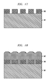
- FIG. 17 is a cross-sectional view illustrating mandrel patterning on the substrate in a method of manufacturing a semiconductor device, according to an exemplary embodiment of the present invention.
- FIG. 18 is a cross-sectional view illustrating dielectric layer deposition in a method of manufacturing a semiconductor device, according to an exemplary embodiment of the present invention.
- FIG. 19 is a cross-sectional view illustrating a result of an annealing process in a method of manufacturing a semiconductor device, according to an exemplary embodiment of the present invention.
- FIG. 20 is a cross-sectional view illustrating removal of unreacted portions of the dielectric layer in a method of manufacturing a semiconductor device, according to an exemplary embodiment of the present invention.
- FIG. 21 is a cross-sectional view illustrating anisotropic removal of horizontal oxide portions in a method of manufacturing a semiconductor device, according to an exemplary embodiment of the present invention.
- FIG. 22 is a cross-sectional view illustrating selective removal of silicon germanium (SiGe) in a method of manufacturing a semiconductor device, according to an exemplary embodiment of the present invention.
- FIG. 23 is a cross-sectional view illustrating removal of exposed portions of the substrate not covered by the remaining portions of oxide to form lines in a method of manufacturing a semiconductor device, according to an exemplary embodiment of the present invention.
- Exemplary embodiments of the invention will now be discussed in further detail with regard to semiconductor devices and methods of manufacturing same and, in particular, to using dielectric material layers and annealing to form tight pitch structures in a substrate.
- CMOS complementary metal-oxide semiconductor
- FET field-effect transistor
- FinFET fin field-effect transistor
- MOSFET metal-oxide-semiconductor field-effect transistor
- SET single electron transistor
- the semiconductor devices and methods for forming same in accordance with embodiments of the present invention can be employed in applications, hardware, and/or electronic systems.
- Suitable hardware and systems for implementing embodiments of the invention may include, but are not limited to, personal computers, communication networks, electronic commerce systems, portable communications devices (e.g., cell and smart phones), solid-state media storage devices, functional circuitry, etc.
- Systems and hardware incorporating the semiconductor devices are contemplated embodiments of the invention. Given the teachings of embodiments of the invention provided herein, one of ordinary skill in the art will be able to contemplate other implementations and applications of embodiments of the invention.
- the embodiments of the present invention can be used in connection with semiconductor devices that may require, for example, FETs, FinFETs, nanowire FETs, nanosheet FETs, vertical FETs, SETs, CMOSs and/or MOSFETs.
- the semiconductor devices can include, but are not necessarily limited to FET, FinFET, nanowire FET, nanosheet FET, vertical FET, SET, CMOS and MOSFET devices, and/or semiconductor devices that use FET, FinFET, nanowire FET, nanosheet FET, vertical FET, SET CMOS and/or, MOSFET technology.
- “height” refers to a vertical size of an element (e.g., a layer, trench, hole, opening, etc.) in the cross-sectional views measured from a bottom surface to a top surface of the element, and/or measured with respect to a surface on which the element is located.
- a “depth” refers to a vertical size of an element (e.g., a layer, trench, hole, opening, etc.) in the three-dimensional views measured from a top surface to a bottom surface of the element. Terms such as “thick”, “thickness”, “thin” or derivatives thereof may be used in place of “height” where indicated.
- lateral refers to a side surface of an element (e.g., a layer, opening, etc.), such as a left or right side surface in the drawings.
- width or “length” refers to a size of an element (e.g., a layer, trench, hole, opening, etc.) in the drawings measured from a side surface to an opposite surface of the element. Terms such as “thick”, “thickness”, “thin” or derivatives thereof may be used in place of “width” or “length” where indicated.
- terms such as “on”, “overlying”, “atop”, “on top”, “positioned on” or “positioned atop” mean that a first element is present on a second element, wherein intervening elements may be present between the first element and the second element.
- the term “directly” used in connection with the terms “on”, “overlying”, “atop”, “on top”, “positioned on” or “positioned atop” or the term “direct contact” mean that a first element and a second element are connected without any intervening elements, such as, for example, intermediary conducting, insulating or semiconductor layers, present between the first element and the second element.
- germanium dioxide (GeO 2 ) spacers and/or layers on amorphous silicon germanium (a-SiGe) mandrels are subjected to an annealing process to form high Ge % SiGe, low Ge % SiGe and silicon oxide portions, which can be patterned and transferred to a substrate to form lines in a tight pitch structure.
- a-SiGe amorphous silicon germanium
- the embodiments of the present invention use SAMP, such as SADP, self-aligned triple patterning (SATP) and SAQP, to form different spacer materials. Patterns of the different spacer materials can be transferred to a substrate to pattern a portion of the substrate into lines at a close pitch with respect to each other.
- the processing forms “lines” in a tight pitch structure without compromising the structure and/or integrity of adjacent lines.
- the lines can form, for example, semiconductor fins or other semiconductor structures at a close pitch with respect to each other.
- the lines may form isolation regions or other insulating structures for a semiconductor device at a close pitch with respect to each other.
- the close (or tight) pitch can be for example, 20 nm to 60 nm between adjacent lines.
- portions of the substrate under the different spacer materials can be removed to form openings (also referred to herein as spaces) in the substrate in a tight pitch structure without compromising the structure and/or integrity of adjacent openings.
- the openings can be formed into, for example, conductive vias or other conductive or contact structures at a close pitch with respect to each other.
- the fill material of the spaces can be, for example, copper, aluminum, cobalt or other electrically conductive material
- the substrate can be a dielectric material.
- the openings can be filled with a dielectric material to form isolation regions or other insulating structures at a close pitch with respect to each other for a semiconductor device.
- the close (or tight) pitch can be for example, 20 nm to 60 nm between adjacent openings.
- FIGS. 1-3 are cross-sectional views illustrating mandrel material deposition, mandrel patterning and spacer formation on a substrate in a method of manufacturing a semiconductor device, according to an exemplary embodiment of the present invention.
- a mandrel material layer 104 comprising amorphous silicon germanium (a-SiGe) is deposited on a substrate 101 .
- a-SiGe amorphous silicon germanium
- the mandrel material layer 104 can be deposited using deposition techniques, such as, for example, chemical vapor deposition (CVD), plasma enhanced CVD (PECVD), radio-frequency CVD (RFCVD), physical vapor deposition (PVD), atomic layer deposition (ALD), molecular layer deposition (MLD), molecular beam deposition (MBD), pulsed laser deposition (PLD), liquid source misted chemical deposition (LSMCD), and/or sputtering.
- CVD chemical vapor deposition
- PECVD plasma enhanced CVD
- RFCVD radio-frequency CVD
- PVD physical vapor deposition
- ALD atomic layer deposition
- MLD molecular layer deposition
- MLD molecular beam deposition
- PLD pulsed laser deposition
- LSMCD liquid source misted chemical deposition
- sputtering sputtering.
- Alternative mandrel materials can include, but are not necessarily limited to, polycrystalline silicon germanium, polycrystalline germanium, and
- a plurality of mandrels 105 are patterned on the substrate 101 .
- the mandrel patterning can be done by various patterning techniques, including, but not necessarily limited to, lithography patterning followed by directional etching and/or a sidewall image transfer (SIT) process, for example.
- the process includes using lithography followed by directional etching (e.g., reactive ion etch (ME)) to form a mandrel 105 .
- a conformal film can be deposited and then followed by an etchback process (e.g., RIE). As shown in FIG.
- the spacer material can include, but is not necessarily limited to, germanium dioxide (GeO 2 ), which can be deposited by low-pressure chemical vapor deposition (LPCVD), plasma enhanced chemical vapor deposition (PECVD), sub-atmospheric chemical vapor deposition (SACVD), rapid thermal chemical vapor deposition (RTCVD), in-situ radical assisted deposition, high temperature oxide deposition (HTO), low temperature oxide deposition (LTO), ozone/TEOS deposition, and/or limited reaction processing CVD (LRPCVD).
- LPCVD low-pressure chemical vapor deposition
- PECVD plasma enhanced chemical vapor deposition
- SACVD sub-atmospheric chemical vapor deposition
- RTCVD rapid thermal chemical vapor deposition
- LTO low temperature oxide deposition
- LTO low temperature oxide deposition
- ozone/TEOS deposition ozone/TEOS deposition
- LPCVD limited reaction processing CVD
- a height of the mandrels 105 and corresponding spacers 107 can be in the range of, but is not necessarily limited to, 30 nm to 100 nm.
- a horizontal width (thickness) of the spacers 107 can be in the range of, but is not necessarily limited to, 10 nm to 50 nm.
- the substrate 101 can include different materials.
- the substrate 101 is formed of a semiconductor material including, but not necessarily limited to, silicon (Si), silicon germanium (SiGe), silicon carbide (SiC), Si:C (carbon doped silicon), silicon germanium carbide (SiGeC), carbon doped silicon germanium (SiGe:C), III-V, II-V compound semiconductor or other like semiconductor.
- a semiconductor material including, but not necessarily limited to, silicon (Si), silicon germanium (SiGe), silicon carbide (SiC), Si:C (carbon doped silicon), silicon germanium carbide (SiGeC), carbon doped silicon germanium (SiGe:C), III-V, II-V compound semiconductor or other like semiconductor.
- the substrate 101 includes a dielectric material such as, but not necessarily limited to, low-k dielectric materials, such as, for example, a silicon oxycarbide, like SiOCH or any suitable dielectric.
- the substrate 101 includes other device structures (not shown) such as transistors, isolation structures (such as shallow trench isolations), contacts, conducting wires, etc.
- the substrate 101 includes both semiconductor materials and dielectric materials, for example, a layer of dielectric material on top of a layer of semiconductor material.
- FIG. 4 is a cross-sectional view illustrating a result of an annealing process in a method of manufacturing a semiconductor device, according to an exemplary embodiment of the present invention.
- a low temperature annealing process is performed to convert the germanium dioxide (GeO 2 ) spacers 107 and convert portions of the a-SiGe mandrels 105 into silicon oxide, such as, but not necessarily limited to, silicon dioxide (SiO 2 ) or SiO x , where x is for example, 1.99 or 2.01, and high germanium (Ge) percentage (%) SiGe, respectively.
- the annealing conditions cause the Si in the a-SiGe mandrel 105 to bond with the oxygen in the GeO 2 spacers 107 to form silicon oxide portions 108 .
- the Si in the a-SiGe mandrel does not bond with the Ge in the GeO 2 spacers 107 .
- the Ge from the GeO 2 spacers 107 is driven into the outer portions of the mandrels 105 and the Si from the outer portions of the mandrels 105 is driven out of the mandrel portions 105 to bond with the oxygen, which forms the high Ge % SiGe portions 109 between the remaining mandrel portions 105 and the silicon oxide portions 108 .
- the resulting Ge concentration in the high Ge % SiGe portions 109 is higher than the Ge concentration in the remaining mandrel portions 105 (also referred to herein as low Ge % SiGe portions).
- the percentage (i.e., concentration) of Ge in the high Ge % SiGe portions 109 is in the range of 30 atomic-90 atomic %, and the percentage (i.e., concentration) of Ge in the low Ge % SiGe portions 105 is in the range of 15 atomic %-50 atomic %.
- the annealing can be performed at a temperature range of 350° C.-700° C., in an environment including nitrogen, argon, xenon, helium, hydrogen, or any suitable combination of those gases, for a time period 1 millisecond to 30 minutes.
- the anneal can be done by rapid thermal annealing (RTP), furnace annealing, flash annealing, laser annealing, spike annealing, or any suitable combination of those techniques.
- the annealing may be carried out for a variable period of time.
- the annealing process is carried out for a time period from about 0.5 seconds to 2 seconds, depending on temperature and germanium concentration in the SiGe mandrel.
- the annealing process may be carried out at a single targeted temperature, or at various ramp and soak cycles using various ramp rates and soak times.
- the silicon from the surface of the a-SiGe mandrel is consumed, and forms silicon oxide portions 108 and high Ge % SiGe portions 109 on outer edges of the remaining mandrel portions 105 .
- the Si atoms in the a-SiGe mandrels 105 bond with available oxygen from the GeO 2 spacers 107 during the annealing process to form silicon oxide portions 108 .
- the high Ge % SiGe portions 109 are formed due to the lower Si concentration and higher Ge concentration caused by the consumption of silicon and influx of germanium in the high Ge % SiGe portions 109 .
- FIG. 5 is a cross-sectional view illustrating selective removal of high Ge % SiGe in a method of manufacturing a semiconductor device, according to an exemplary embodiment of the present invention.
- the high Ge % SiGe portions 109 are selectively removed with respect to the remaining mandrel portions 105 and the silicon oxide portions 108 .
- An etching process that selectively removes the high Ge % SiGe portions 109 with respect to the remaining mandrel portions 105 and the silicon oxide portions 108 is performed.
- the selective removal can be performed using, for example, gas phase hydrogen fluoride or a wet etch process containing a mix of ammonia and hydrogen peroxide, and is performed down to the substrate 101 .
- FIG. 6 is a cross-sectional view illustrating mask formation and selective removal of an exposed portion of the mandrel material in a method of manufacturing a semiconductor device, according to an exemplary embodiment of the present invention.
- a mask 115 such as, for example, a photoresist including an optical planarization layer (OPL) is formed on the substrate 101 and on and around the remaining mandrel portions 105 and the silicon oxide portions 108 .
- OPL optical planarization layer
- the mask 115 leaves exposed a mandrel portion 105 that is to be removed.
- any number of mandrel portions 105 can be left exposed to be removed.
- the mask 115 can leave exposed silicon oxide portions 108 which are adjacent the mandrel portion 105 that is to be removed. As shown by the phantom lines 117 , the exposed mandrel portion 105 is removed using an etching process which is selective with respect to the material of the silicon oxide portions 108 .
- the mandrel portion 105 can be selectively etched using any suitable etch process, for example, gas phase hydrogen fluoride, a wet etch process containing a mix of ammonia and hydrogen peroxide, or a dry etch such as a plasma etch.
- gas phase hydrogen fluoride for example, gas phase hydrogen fluoride, a wet etch process containing a mix of ammonia and hydrogen peroxide, or a dry etch such as a plasma etch.
- FIG. 7 is a cross-sectional view illustrating mask formation and selective removal of an exposed portion of an oxide in a method of manufacturing a semiconductor device, according to an exemplary embodiment of the present invention.
- a mask 125 such as, for example, a photoresist including an optical planarization layer (OPL)
- OPL optical planarization layer
- the mask 115 can be removed by, for example, oxygen plasma etch.
- the mask 125 leaves exposed a silicon oxide portion 108 that is to be removed. Depending on design constraints, and the desired resulting structure of lines and/or spaces, any number of silicon oxide portions 108 can be left exposed to be removed. Since the material of the silicon oxide portions 108 is different from the mandrel material and can be selectively removed with respect to the mandrel material, the mask 125 can leave mandrel portions 105 which are adjacent the silicon oxide portion 108 that is to be removed. As shown by the phantom lines 127 , the exposed silicon oxide portion 108 is removed using an etching process which is selective with respect to the mandrel material.
- the silicon oxide portion 108 can be selectively etched using, for example, a wet etch process including hydrofluoric acid (HF).
- HF hydrofluoric acid
- silicon oxide can be removed by dry etch such as chemical oxide removal (COR) or a plasma etch.
- FIG. 8 is a cross-sectional view illustrating mask removal
- FIG. 9 is a cross-sectional view illustrating removal of exposed portions of the substrate not covered by the remaining portions of the mandrel material and oxide to form lines in a method of manufacturing a semiconductor device, according to an exemplary embodiment of the present invention.
- the mask 125 is removed using, for example, oxygen plasma etch.
- exposed portions of the substrate 101 not covered by the remaining mandrel portions 105 and silicon oxide portions 108 are removed to a certain depth d 1 (depending on design) using a substrate etch.
- substrate 101 including a semiconductor material, such as, Si, SiGe, SiC, Si:C, SiGeC, SiGe:C, II-V compound semiconductor or other like semiconductor can be selectively etched with respect to the remaining mandrel portions 105 and silicon oxide portions 108 using, for example, a silicon RIE process, and substrate 101 including a dielectric material, such as, but not necessarily limited to, SiOCH can be selectively etched with respect to the remaining mandrel portions 105 and silicon oxide portions 108 using, for example, CF 4 or N 2 /H 2 plasma.
- a semiconductor material such as, Si, SiGe, SiC, Si:C, SiGeC, SiGe:C, II-V compound semiconductor or other like semiconductor
- substrate 101 including a dielectric material, such as, but not necessarily limited to, SiOCH can be selectively etched with respect to the remaining mandrel portions 105 and silicon oxide portions 108 using, for example, CF 4 or N 2 /H 2 plasma.
- a hardmask layer e.g., silicon nitride (SiN)
- SiN silicon nitride
- the hardmask layer can be deposited on top of the SiGe substrate prior to forming the SiGe mandrels.
- the remaining mandrel and silicon oxide portions can be used when etching the SiN hardmask layer as the mask layers to pattern the SiN hardmask.
- the processing forms lines 101 ′ in a tight pitch structure (e.g., 20 nm to 60 nm between adjacent lines) without compromising the structure and/or integrity of adjacent lines 101 ′.
- the lines 101 ′ can form, for example, semiconductor fins or other semiconductor structures, or isolation regions or other insulating structures at a close pitch with respect to each other.
- FIGS. 10-12 are cross-sectional views illustrating mandrel material deposition, mandrel patterning and spacer formation on a substrate in a method of manufacturing a semiconductor device, according to an exemplary embodiment of the present invention.
- a mandrel material layer 204 comprising amorphous silicon germanium (a-SiGe) is deposited on a substrate 201 .
- the mandrel material layer 204 can be deposited using deposition techniques, such as, for example, CVD, PECVD, RFCVD, PVD, ALD, MLD, MBD, PLD, LSMCD, and/or sputtering.
- Alternative mandrel materials can include, but are not necessarily limited to, polycrystalline silicon germanium, polycrystalline germanium, and amorphous germanium.
- a plurality of mandrels 205 are patterned on the substrate 201 .
- the mandrel patterning can be done by various patterning techniques, including, but not necessarily limited to, lithography patterning followed by directional etching and/or a sidewall image transfer (SIT) process, for example.
- a conformal film can be deposited and then followed by an etchback process (e.g., RIE).
- RIE sidewall image transfer
- the conformal film will form spacers 207 at both sides of each mandrel 205 .
- the spacer material can include, but is not necessarily limited to, germanium dioxide (GeO 2 ), which can be deposited by LPCVD, PECVD, SACVD, RTCVD, in-situ radical assisted deposition, HTO deposition, LTO deposition, ozone/TEOS deposition, and/or LRPCVD.
- a height of the mandrels 205 and corresponding spacers 207 can be in the range of, but is not necessarily limited to, 30 nm to 100 nm.
- a horizontal width (thickness) of the spacers 207 can be in the range of, but is not necessarily limited to, 10 nm to 50 nm.
- the substrate 201 can include semiconductor or dielectric materials, and can include other device structures (not shown) such as transistors, isolation structures (such as shallow trench isolations), contacts, conducting wires, etc.
- FIG. 13 is a cross-sectional view illustrating mandrel material deposition to fill in vacant areas on the substrate and planarization in a method of manufacturing a semiconductor device, according to an exemplary embodiment of the present invention.
- the mandrel material such as a-SiGe
- the deposited layer 210 is planarized to the top surface of the spacers 207 and the top surface of the mandrels 205 to result in the structure shown in FIG. 13 .
- the mandrel material can be deposited using deposition techniques, including, but not limited to, CVD, LPCVD, PECVD, LPCVD, RFCVD, PVD, ALD, MLD, MBD, PLD, LSMCD, spin-on, and/or sputtering, and the planarization can be performed using, for example, chemical mechanical planarization (CMP).
- CVD chemical mechanical planarization
- FIG. 14 is a cross-sectional view illustrating a result of an annealing process in a method of manufacturing a semiconductor device, according to an exemplary embodiment of the present invention.
- a low temperature annealing process is performed to convert the germanium dioxide (GeO 2 ) spacers 207 and convert portions of the a-SiGe mandrels 205 into silicon oxide (e.g., SiO 2 and SiO x ) and high Ge % SiGe, respectively.
- silicon oxide e.g., SiO 2 and SiO x
- the annealing conditions cause the Si in the a-SiGe mandrel 205 to bond with the oxygen in the GeO 2 spacers 207 to form silicon oxide portions 208 .
- the Si in the a-SiGe mandrel does not bond with the Ge in the GeO 2 spacers 207 .
- the Ge from the GeO 2 spacers 207 is driven into the outer portions of the mandrels 205 and the Si from the outer portions of the mandrels 205 is driven out of the mandrel portions 205 to bond with the oxygen, which forms the high Ge % SiGe portions 209 between the remaining mandrel portions 205 and the silicon oxide portions 208 .
- the resulting Ge concentration in the high Ge % SiGe portions 209 is higher than the Ge concentration in the remaining mandrel portions 205 (also referred to herein as low Ge % SiGe portions).
- the percentage (i.e., concentration) of Ge in the high Ge % SiGe portions 209 is in the range of 30 atomic % to 90 atomic %
- the percentage (i.e., concentration) of Ge in the low Ge % SiGe portions 205 is in the range of 15 atomic % to 50 atomic %.
- the annealing conditions for the embodiment described in connection with FIG. 14 can be the same or similar to those described in connection with FIG. 4 .
- FIG. 15 is a cross-sectional view illustrating selective removal of mandrel material and oxide in a method of manufacturing a semiconductor device, according to an exemplary embodiment of the present invention.
- the remaining mandrel portions 205 i.e., low Ge % SiGe portions
- the silicon oxide portions 208 are selectively removed with respect to the high Ge % SiGe portions 209 .
- An etching process that selectively removes the remaining mandrel portions 205 and the silicon oxide portions 208 with respect to the high Ge % SiGe portions 209 is performed.
- the selective removal performed down to the substrate 201 can be performed using, for example, a silicon oxide etch selective to high Ge % SiGe, such as a wet etch process including hydrofluoric acid (HF).
- silicon oxide can be removed by a dry etch such as chemical oxide removal (COR) or plasma etch.
- a low Ge % SiGe etch selective to high Ge % SiGe includes, for example, a wet etch containing ammonia.
- FIG. 16 is a cross-sectional view illustrating removal of exposed portions of the substrate not covered by the remaining portions of high germanium (Ge) percentage (%) silicon germanium (SiGe) to form lines in a method of manufacturing a semiconductor device, according to an exemplary embodiment of the present invention.
- Ga germanium
- SiGe silicon germanium
- substrate 201 including a semiconductor material such as, Si, SiGe, SiC, Si:C, SiGeC, SiGe:C, II-V compound semiconductor or other like semiconductor
- substrate 201 including a dielectric material such as, but not necessarily limited to, SiOCH can be selectively etched with respect to the remaining high Ge % SiGe portions 209 using, for example, CF 4 or N 2 /H 2 plasma.
- the processing forms lines 201 ′ in a tight pitch structure (e.g., 20 nm to 60 nm between adjacent lines) without compromising the structure and/or integrity of adjacent lines 201 ′.
- the lines 201 ′ can form, for example, semiconductor fins or other semiconductor structures, or isolation regions or other insulating structures at a close pitch with respect to each other.
- a hardmask layer e.g., silicon nitride (SiN)
- SiN silicon nitride
- FIG. 17 is a cross-sectional view illustrating mandrel patterning on the substrate in a method of manufacturing a semiconductor device, according to an exemplary embodiment of the present invention.
- a mandrel material layer comprising, for example, amorphous silicon germanium (a-SiGe)
- a plurality of mandrels 305 are patterned on the substrate 301 .
- the mandrel patterning can be done by various patterning techniques, including, but not necessarily limited to, lithography patterning followed by directional etching and/or a sidewall image transfer (SIT) process, for example.
- SIT sidewall image transfer
- Mandrel materials can include, but are not necessarily limited to, polycrystalline silicon germanium, polycrystalline germanium, and amorphous germanium.
- a height of the mandrels 305 can be in the range of, but is not necessarily limited to, 30 nm to 100 nm.
- the substrate 301 can include semiconductor or dielectric materials, and can include other device structures (not shown) such as transistors, isolation structures (such as shallow trench isolations), contacts, conducting wires, etc.
- FIG. 18 is a cross-sectional view illustrating dielectric layer deposition in a method of manufacturing a semiconductor device, according to an exemplary embodiment of the present invention.
- a dielectric layer 307 is deposited over the structure in FIG. 17 , using deposition techniques, such as, for example, CVD, LPCVD, PECVD, LPCVD, RFCVD, PVD, ALD, MLD, MBD, PLD, LSMCD, spin-on, and/or sputtering.
- the layer 307 includes GeO 2 , and a planarization/polishing process is not performed on the deposited layer 307 .
- a height of the dielectric layer 307 can be in the range of, but is not necessarily limited to, 100 nm-150 nm.
- FIG. 19 is a cross-sectional view illustrating a result of an annealing process in a method of manufacturing a semiconductor device, according to an exemplary embodiment of the present invention.
- an annealing process is performed to convert portions of the GeO 2 layer 307 and convert portions of the a-SiGe mandrels 305 into silicon oxide (e.g., SiO 2 or SiO x ) and high Ge % SiGe, respectively.
- silicon oxide e.g., SiO 2 or SiO x
- the annealing conditions cause the Si in the a-SiGe mandrel 305 to bond with the oxygen in the portions of the GeO 2 layer 307 on side and top surfaces of the mandrels 305 to form silicon oxide portions 308 on top and side surfaces of the mandrels 305 .
- the Si in the a-SiGe mandrel does not bond with the Ge in the GeO 2 layer 307 .
- the Ge from the GeO 2 layer 307 is driven into the outer portions of the mandrels 305 and the Si from the outer portions of the mandrels 305 is driven out of the mandrel portions 305 to bond with the oxygen, which forms the high Ge % SiGe portions 309 on the top and side surfaces of the remaining mandrel portions 305 between the remaining mandrel portions 305 and the silicon oxide portions 308 .
- the resulting Ge concentration in the high Ge % SiGe portions 309 is higher than the Ge concentration in the remaining mandrel portions 305 (also referred to herein as low Ge % SiGe portions).
- the percentage (i.e., concentration) of Ge in the high Ge % SiGe portions 309 is in the range of 50 atomic % to 90 atomic %, and the percentage (i.e., concentration) of Ge in the low Ge % SiGe portions 305 is in the range of 15 atomic % to 30 atomic %.
- the annealing is a spike anneal carried out in a nitrogen (N 2 ) ambient at less than 500° C.
- the annealing can be performed at a temperature range of 350° C.-700° C., in an environment including nitrogen, argon, xenon, helium, hydrogen, or any suitable combination of those gases, for a time period 1 millisecond to 30 minutes.
- the anneal can be done by rapid thermal annealing (RTP), furnace annealing, flash annealing, laser annealing, spike annealing, or any suitable combination of those techniques.
- the annealing may be carried out for a variable period of time.
- the annealing process is carried out for a time period from about 0.5 seconds to 2 seconds, depending on temperature and germanium concentration in the SiGe mandrel.
- the annealing process may be carried out at a single targeted temperature, or at various ramp and soak cycles using various ramp rates and soak times.
- FIG. 20 is a cross-sectional view illustrating removal of unreacted portions of the dielectric layer in a method of manufacturing a semiconductor device, according to an exemplary embodiment of the present invention.
- unreacted portions of the dielectric layer e.g., GeO 2 that has not been converted to silicon oxide
- DIW deionized water
- FIG. 21 is a cross-sectional view illustrating anisotropic removal of horizontal oxide portions in a method of manufacturing a semiconductor device, according to an exemplary embodiment of the present invention.
- an anisotropic etching process e.g., ME
- the etching can be performed using, for example, an oxide ME process to remove the horizontal parts of the silicon oxide portions 308 .
- FIG. 22 is a cross-sectional view illustrating selective removal of silicon germanium (SiGe) in a method of manufacturing a semiconductor device, according to an exemplary embodiment of the present invention.
- SiGe silicon germanium
- the SiGe portions 305 and 309 e.g., low and high Ge % SiGe portions
- the SiGe portions 305 and 309 are removed using an etching process which is selective with respect to the material of the silicon oxide portions 308 .
- the SiGe portions 305 and 309 include low and high Ge % SiGe, and the material of the silicon oxide portions 308 includes silicon oxide, then the SiGe portions 305 and 309 can be selectively etched using any suitable etch process, for example, gas phase hydrogen fluoride, a wet etch process containing a mix of ammonia and hydrogen peroxide, or a dry etch such as a plasma etch.
- etch process for example, gas phase hydrogen fluoride, a wet etch process containing a mix of ammonia and hydrogen peroxide, or a dry etch such as a plasma etch.
- FIG. 23 is a cross-sectional view illustrating removal of exposed portions of the substrate not covered by the remaining portions of oxide to form lines in a method of manufacturing a semiconductor device, according to an exemplary embodiment of the present invention.
- exposed portions of the substrate 301 not covered by the remaining silicon oxide portions 308 are removed to a certain depth d 3 (depending on design) using a substrate etch.
- the substrate etch transfers the pattern of the remaining silicon oxide portions 308 to the substrate to form patterned substrate portions 301 ′.
- substrate 301 including a semiconductor material such as, Si, SiGe, SiC, Si:C, SiGeC, SiGe:C, III-V, II-V compound semiconductor or other like semiconductor
- substrate 301 including a dielectric material such as, but not necessarily limited to, SiOCH can be selectively etched with respect to the silicon oxide portions 308 using, for example, CF 4 or N 2 /H 2 plasma.
- the processing forms lines 301 ′ in a tight pitch structure (e.g., 20 nm to 60 nm between adjacent lines) without compromising the structure and/or integrity of adjacent lines 301 ′.
- the lines 301 ′ can form, for example, semiconductor fins or other semiconductor structures, or isolation regions or other insulating structures at a close pitch with respect to each other.
Landscapes
- Engineering & Computer Science (AREA)
- Manufacturing & Machinery (AREA)
- Insulated Gate Type Field-Effect Transistor (AREA)
- Thin Film Transistor (AREA)
Abstract
Description
Claims (16)
Priority Applications (1)
| Application Number | Priority Date | Filing Date | Title |
|---|---|---|---|
| US15/846,779 US10424482B2 (en) | 2017-12-19 | 2017-12-19 | Methods and structures for forming a tight pitch structure |
Applications Claiming Priority (1)
| Application Number | Priority Date | Filing Date | Title |
|---|---|---|---|
| US15/846,779 US10424482B2 (en) | 2017-12-19 | 2017-12-19 | Methods and structures for forming a tight pitch structure |
Publications (2)
| Publication Number | Publication Date |
|---|---|
| US20190189443A1 US20190189443A1 (en) | 2019-06-20 |
| US10424482B2 true US10424482B2 (en) | 2019-09-24 |
Family
ID=66816305
Family Applications (1)
| Application Number | Title | Priority Date | Filing Date |
|---|---|---|---|
| US15/846,779 Expired - Fee Related US10424482B2 (en) | 2017-12-19 | 2017-12-19 | Methods and structures for forming a tight pitch structure |
Country Status (1)
| Country | Link |
|---|---|
| US (1) | US10424482B2 (en) |
Families Citing this family (1)
| Publication number | Priority date | Publication date | Assignee | Title |
|---|---|---|---|---|
| US10763118B2 (en) * | 2018-07-11 | 2020-09-01 | International Business Machines Corporation | Cyclic selective deposition for tight pitch patterning |
Citations (13)
| Publication number | Priority date | Publication date | Assignee | Title |
|---|---|---|---|---|
| US20050020020A1 (en) | 2002-07-16 | 2005-01-27 | Nadine Collaert | Integrated semiconductor fin device and a method for manufacturing such device |
| US20050169096A1 (en) | 2003-07-01 | 2005-08-04 | Lee Hyo-San | PAA- based etchant, methods of using same, and resultant structures |
| US20130020707A1 (en) | 2011-06-28 | 2013-01-24 | Monolithic 3D Inc. | Novel semiconductor system and device |
| US8716156B1 (en) | 2013-02-01 | 2014-05-06 | Globalfoundries Inc. | Methods of forming fins for a FinFET semiconductor device using a mandrel oxidation process |
| US20140264755A1 (en) * | 2013-03-13 | 2014-09-18 | International Business Machines Corporation | Strained silicon nfet and silicon germanium pfet on same wafer |
| US20140374838A1 (en) | 2013-06-21 | 2014-12-25 | Taiwan Semiconductor Manufacturing Company, Ltd. | FinFETs with Nitride Liners and Methods of Forming the Same |
| US9276013B1 (en) * | 2015-01-21 | 2016-03-01 | International Business Machines Corporation | Integrated formation of Si and SiGe fins |
| US20160086796A1 (en) * | 2014-09-22 | 2016-03-24 | International Business Machines Corporation | Self-forming spacers using oxidation |
| US9312183B1 (en) | 2014-11-03 | 2016-04-12 | Globalfoundries Inc. | Methods for forming FinFETS having a capping layer for reducing punch through leakage |
| US20160322501A1 (en) * | 2015-04-29 | 2016-11-03 | International Business Machines Corporation | Silicon germanium alloy fins with reduced defects |
| US20160336236A1 (en) | 2015-02-24 | 2016-11-17 | International Business Machines Corporation | Dual fin integration for electron and hole mobility enhancement |
| US20160365286A1 (en) * | 2015-06-15 | 2016-12-15 | International Business Machines Corporation | Semiconductor fins for finfet devices and sidewall image transfer (sit) processes for manufacturing the same |
| US20170005180A1 (en) | 2015-06-30 | 2017-01-05 | International Business Machines Corporation | Internal spacer formation from selective oxidation for fin-first wire-last replacement gate-all-around nanowire fet |
-
2017
- 2017-12-19 US US15/846,779 patent/US10424482B2/en not_active Expired - Fee Related
Patent Citations (16)
| Publication number | Priority date | Publication date | Assignee | Title |
|---|---|---|---|---|
| US20050020020A1 (en) | 2002-07-16 | 2005-01-27 | Nadine Collaert | Integrated semiconductor fin device and a method for manufacturing such device |
| US6974729B2 (en) | 2002-07-16 | 2005-12-13 | Interuniversitair Microelektronica Centrum (Imec) | Integrated semiconductor fin device and a method for manufacturing such device |
| US20050169096A1 (en) | 2003-07-01 | 2005-08-04 | Lee Hyo-San | PAA- based etchant, methods of using same, and resultant structures |
| US7709277B2 (en) | 2003-07-01 | 2010-05-04 | Samsung Electronics Co., Ltd. | PAA-based etchant, methods of using same, and resultant structures |
| US9219005B2 (en) | 2011-06-28 | 2015-12-22 | Monolithic 3D Inc. | Semiconductor system and device |
| US20130020707A1 (en) | 2011-06-28 | 2013-01-24 | Monolithic 3D Inc. | Novel semiconductor system and device |
| US8716156B1 (en) | 2013-02-01 | 2014-05-06 | Globalfoundries Inc. | Methods of forming fins for a FinFET semiconductor device using a mandrel oxidation process |
| US20140264755A1 (en) * | 2013-03-13 | 2014-09-18 | International Business Machines Corporation | Strained silicon nfet and silicon germanium pfet on same wafer |
| US20140374838A1 (en) | 2013-06-21 | 2014-12-25 | Taiwan Semiconductor Manufacturing Company, Ltd. | FinFETs with Nitride Liners and Methods of Forming the Same |
| US20160086796A1 (en) * | 2014-09-22 | 2016-03-24 | International Business Machines Corporation | Self-forming spacers using oxidation |
| US9312183B1 (en) | 2014-11-03 | 2016-04-12 | Globalfoundries Inc. | Methods for forming FinFETS having a capping layer for reducing punch through leakage |
| US9276013B1 (en) * | 2015-01-21 | 2016-03-01 | International Business Machines Corporation | Integrated formation of Si and SiGe fins |
| US20160336236A1 (en) | 2015-02-24 | 2016-11-17 | International Business Machines Corporation | Dual fin integration for electron and hole mobility enhancement |
| US20160322501A1 (en) * | 2015-04-29 | 2016-11-03 | International Business Machines Corporation | Silicon germanium alloy fins with reduced defects |
| US20160365286A1 (en) * | 2015-06-15 | 2016-12-15 | International Business Machines Corporation | Semiconductor fins for finfet devices and sidewall image transfer (sit) processes for manufacturing the same |
| US20170005180A1 (en) | 2015-06-30 | 2017-01-05 | International Business Machines Corporation | Internal spacer formation from selective oxidation for fin-first wire-last replacement gate-all-around nanowire fet |
Non-Patent Citations (1)
| Title |
|---|
| E. Chong et al., "Hard Mask Profile and Loading Issue Study in SADP Process," China Semiconductor Technology International Conference (CSTIC), Mar. 15-16, 2015, 3 pages. |
Also Published As
| Publication number | Publication date |
|---|---|
| US20190189443A1 (en) | 2019-06-20 |
Similar Documents
| Publication | Publication Date | Title |
|---|---|---|
| CN107275281B (en) | Self-aligned contact scheme, semiconductor structure and forming method thereof | |
| US10355108B2 (en) | Method of forming a fin field effect transistor comprising two etching steps to define a fin structure | |
| US10867862B2 (en) | Semiconductor method and device | |
| CN110957259A (en) | Method of forming semiconductor device | |
| TWI882052B (en) | Semiconductor device and method of manufacturing the same | |
| US9870951B2 (en) | Method of fabricating semiconductor structure with self-aligned spacers | |
| JP7745765B2 (en) | Gate-all-around transistor architecture with filled dielectric material - Patents.com | |
| CN110660862B (en) | Semiconductor devices and methods | |
| US20240021619A1 (en) | Finfet device and method | |
| TW202217974A (en) | Semiconductor device and method of forming same | |
| TWI872260B (en) | Semiconductor device and method of forming the same | |
| TW202213467A (en) | Semiconductor device and method of forming same | |
| TW202109623A (en) | Method for forming semiconductor device | |
| TW202133269A (en) | Method forming semiconductor device | |
| US10991584B2 (en) | Methods and structures for cutting lines or spaces in a tight pitch structure | |
| KR20230165136A (en) | Semiconductor devices including backside power via and methods of forming the same | |
| JP2025507548A (en) | Gate-all-around backside power rail with diffusion blocking | |
| US10424482B2 (en) | Methods and structures for forming a tight pitch structure | |
| US20240387255A1 (en) | Device and method of forming the same | |
| TWI865137B (en) | Methods of forming semiconductor device | |
| TWI852433B (en) | Semiconductor device and method for manufacturing the same | |
| US10943816B2 (en) | Mask removal for tight-pitched nanostructures | |
| US7989300B2 (en) | Method of manufacturing semiconductor device | |
| TWI905498B (en) | Semiconductor device and manufacturing method thereof | |
| CN217655884U (en) | Semiconductor device with a plurality of semiconductor chips |
Legal Events
| Date | Code | Title | Description |
|---|---|---|---|
| AS | Assignment |
Owner name: INTERNATIONAL BUSINESS MACHINES CORPORATION, NEW Y Free format text: ASSIGNMENT OF ASSIGNORS INTEREST;ASSIGNORS:XU, PENG;CHENG, KANGGUO;LEE, CHOONGHYUN;AND OTHERS;REEL/FRAME:044433/0853 Effective date: 20171215 |
|
| FEPP | Fee payment procedure |
Free format text: ENTITY STATUS SET TO UNDISCOUNTED (ORIGINAL EVENT CODE: BIG.); ENTITY STATUS OF PATENT OWNER: LARGE ENTITY |
|
| STPP | Information on status: patent application and granting procedure in general |
Free format text: NOTICE OF ALLOWANCE MAILED -- APPLICATION RECEIVED IN OFFICE OF PUBLICATIONS |
|
| STPP | Information on status: patent application and granting procedure in general |
Free format text: PUBLICATIONS -- ISSUE FEE PAYMENT VERIFIED |
|
| STCF | Information on status: patent grant |
Free format text: PATENTED CASE |
|
| AS | Assignment |
Owner name: ELPIS TECHNOLOGIES INC., CANADA Free format text: ASSIGNMENT OF ASSIGNORS INTEREST;ASSIGNOR:INTERNATIONAL BUSINESS MACHINES CORPORATION;REEL/FRAME:052561/0161 Effective date: 20200306 |
|
| FEPP | Fee payment procedure |
Free format text: MAINTENANCE FEE REMINDER MAILED (ORIGINAL EVENT CODE: REM.); ENTITY STATUS OF PATENT OWNER: LARGE ENTITY |
|
| LAPS | Lapse for failure to pay maintenance fees |
Free format text: PATENT EXPIRED FOR FAILURE TO PAY MAINTENANCE FEES (ORIGINAL EVENT CODE: EXP.); ENTITY STATUS OF PATENT OWNER: LARGE ENTITY |
|
| STCH | Information on status: patent discontinuation |
Free format text: PATENT EXPIRED DUE TO NONPAYMENT OF MAINTENANCE FEES UNDER 37 CFR 1.362 |
|
| FP | Lapsed due to failure to pay maintenance fee |
Effective date: 20230924 |