US10403435B2 - Edder compound and capacitor thereof - Google Patents
Edder compound and capacitor thereof Download PDFInfo
- Publication number
- US10403435B2 US10403435B2 US15/844,364 US201715844364A US10403435B2 US 10403435 B2 US10403435 B2 US 10403435B2 US 201715844364 A US201715844364 A US 201715844364A US 10403435 B2 US10403435 B2 US 10403435B2
- Authority
- US
- United States
- Prior art keywords
- electron
- metadielectric
- insulating
- group
- film
- Prior art date
- Legal status (The legal status is an assumption and is not a legal conclusion. Google has not performed a legal analysis and makes no representation as to the accuracy of the status listed.)
- Active
Links
- 239000003990 capacitor Substances 0.000 title description 48
- 150000001875 compounds Chemical class 0.000 title description 8
- 239000002131 composite material Substances 0.000 claims abstract description 33
- 239000011368 organic material Substances 0.000 claims abstract description 8
- 229920000642 polymer Polymers 0.000 claims description 31
- 239000000463 material Substances 0.000 claims description 29
- -1 polyalkylacrylate Polymers 0.000 claims description 17
- 125000003118 aryl group Chemical group 0.000 claims description 16
- 125000000217 alkyl group Chemical group 0.000 claims description 10
- 229920000728 polyester Polymers 0.000 claims description 10
- 229910052760 oxygen Inorganic materials 0.000 claims description 6
- 229910052799 carbon Inorganic materials 0.000 claims description 5
- 125000005842 heteroatom Chemical group 0.000 claims description 5
- 229910052717 sulfur Inorganic materials 0.000 claims description 5
- 229920001577 copolymer Polymers 0.000 claims description 4
- 239000004952 Polyamide Substances 0.000 claims description 3
- 229920003235 aromatic polyamide Polymers 0.000 claims description 3
- 125000000753 cycloalkyl group Chemical group 0.000 claims description 3
- 229910052757 nitrogen Inorganic materials 0.000 claims description 3
- 229920002647 polyamide Polymers 0.000 claims description 3
- 150000008282 halocarbons Chemical class 0.000 claims 4
- 229920006395 saturated elastomer Polymers 0.000 claims 2
- 229930195734 saturated hydrocarbon Natural products 0.000 claims 2
- 239000000178 monomer Substances 0.000 abstract description 46
- 238000004768 lowest unoccupied molecular orbital Methods 0.000 abstract description 4
- 0 *1C(N=C*2)=C2N=C1 Chemical compound *1C(N=C*2)=C2N=C1 0.000 description 122
- 239000010408 film Substances 0.000 description 31
- 239000003989 dielectric material Substances 0.000 description 24
- 230000015556 catabolic process Effects 0.000 description 20
- 239000000370 acceptor Substances 0.000 description 18
- 238000004146 energy storage Methods 0.000 description 16
- 229910052751 metal Inorganic materials 0.000 description 14
- 239000002184 metal Substances 0.000 description 14
- 239000004973 liquid crystal related substance Substances 0.000 description 11
- 125000004122 cyclic group Chemical group 0.000 description 8
- 230000005684 electric field Effects 0.000 description 8
- OKTJSMMVPCPJKN-UHFFFAOYSA-N Carbon Chemical compound [C] OKTJSMMVPCPJKN-UHFFFAOYSA-N 0.000 description 7
- 125000001072 heteroaryl group Chemical group 0.000 description 6
- 238000000034 method Methods 0.000 description 6
- 239000000203 mixture Substances 0.000 description 6
- 229920003023 plastic Polymers 0.000 description 6
- 239000004033 plastic Substances 0.000 description 6
- 239000004743 Polypropylene Substances 0.000 description 5
- 229920001155 polypropylene Polymers 0.000 description 5
- 239000005266 side chain polymer Substances 0.000 description 5
- 239000007787 solid Substances 0.000 description 5
- 239000000758 substrate Substances 0.000 description 5
- UJOBWOGCFQCDNV-UHFFFAOYSA-N 9H-carbazole Chemical compound C1=CC=C2C3=CC=CC=C3NC2=C1 UJOBWOGCFQCDNV-UHFFFAOYSA-N 0.000 description 4
- UHOVQNZJYSORNB-UHFFFAOYSA-N Benzene Chemical compound C1=CC=CC=C1 UHOVQNZJYSORNB-UHFFFAOYSA-N 0.000 description 4
- 239000004734 Polyphenylene sulfide Substances 0.000 description 4
- FZWLAAWBMGSTSO-UHFFFAOYSA-N Thiazole Chemical compound C1=CSC=N1 FZWLAAWBMGSTSO-UHFFFAOYSA-N 0.000 description 4
- YTPLMLYBLZKORZ-UHFFFAOYSA-N Thiophene Chemical compound C=1C=CSC=1 YTPLMLYBLZKORZ-UHFFFAOYSA-N 0.000 description 4
- 125000005605 benzo group Chemical group 0.000 description 4
- 230000000903 blocking effect Effects 0.000 description 4
- 239000004020 conductor Substances 0.000 description 4
- 239000011810 insulating material Substances 0.000 description 4
- 239000004014 plasticizer Substances 0.000 description 4
- 229920000069 polyphenylene sulfide Polymers 0.000 description 4
- 239000004810 polytetrafluoroethylene Substances 0.000 description 4
- 229920001343 polytetrafluoroethylene Polymers 0.000 description 4
- 239000002904 solvent Substances 0.000 description 4
- BQTJMKIHKULPCZ-UHFFFAOYSA-N C1=CC2=CCC=C2C=C1 Chemical compound C1=CC2=CCC=C2C=C1 BQTJMKIHKULPCZ-UHFFFAOYSA-N 0.000 description 3
- OUJRXIZLOYCVEX-BZAYTVMESA-N CC1=CC(C#CC2=CC=C3C(=C2)[Y]C(=O)/C3=C2/C(=O)[Y]C3=C2C=CC(C#CC2=CC=C([N+](=O)[O-])C([N+](=O)[O-])=C2)=C3)=CC(C)=C1C Chemical compound CC1=CC(C#CC2=CC=C3C(=C2)[Y]C(=O)/C3=C2/C(=O)[Y]C3=C2C=CC(C#CC2=CC=C([N+](=O)[O-])C([N+](=O)[O-])=C2)=C3)=CC(C)=C1C OUJRXIZLOYCVEX-BZAYTVMESA-N 0.000 description 3
- FPGIXJBLPLRSFB-UHFFFAOYSA-N CCCCCCC1=C(C2=CC(CCCCCC)=C(N(C)C)S2)SC(C2=CC=C(C3=CC=C(C4=C5C(=O)N(C)C(=O)C5=C(C5=CC=C([N+](=O)[O-])C=C5)S4)S3)S2)=C1 Chemical compound CCCCCCC1=C(C2=CC(CCCCCC)=C(N(C)C)S2)SC(C2=CC=C(C3=CC=C(C4=C5C(=O)N(C)C(=O)C5=C(C5=CC=C([N+](=O)[O-])C=C5)S4)S3)S2)=C1 FPGIXJBLPLRSFB-UHFFFAOYSA-N 0.000 description 3
- BMGDNRSEDDWRCA-BYYHNAKLSA-N CN(C)C1=C2OCCOC2=C(C2=CC=C(C3=CC=C(C4=CC=C(/N=N/C5=CC=C([N+](=O)[O-])C=C5)S4)S3)S2)S1 Chemical compound CN(C)C1=C2OCCOC2=C(C2=CC=C(C3=CC=C(C4=CC=C(/N=N/C5=CC=C([N+](=O)[O-])C=C5)S4)S3)S2)S1 BMGDNRSEDDWRCA-BYYHNAKLSA-N 0.000 description 3
- JOEFCZNQFJSUIY-UHFFFAOYSA-N CN(C)C1=CN=C(C2=CC=C(C3=CC4=C(C=C(C5=CC=C(S(=O)(=O)N(C)C)C=C5)C5=NSN=C54)C4=NSN=C34)S2)S1 Chemical compound CN(C)C1=CN=C(C2=CC=C(C3=CC4=C(C=C(C5=CC=C(S(=O)(=O)N(C)C)C=C5)C5=NSN=C54)C4=NSN=C34)S2)S1 JOEFCZNQFJSUIY-UHFFFAOYSA-N 0.000 description 3
- FPOQDVLTVRHUOU-XPLMANRPSA-N [C-]#[N+]/C(C#N)=C\C1=CC=C(/N=N/C2=CC=C(C3=CC=C(C4=CC=C(C5=C6OCCOC6=C(N(C)C)S5)S4)S3)S2)C=C1 Chemical compound [C-]#[N+]/C(C#N)=C\C1=CC=C(/N=N/C2=CC=C(C3=CC=C(C4=CC=C(C5=C6OCCOC6=C(N(C)C)S5)S4)S3)S2)C=C1 FPOQDVLTVRHUOU-XPLMANRPSA-N 0.000 description 3
- HSFWRNGVRCDJHI-UHFFFAOYSA-N alpha-acetylene Natural products C#C HSFWRNGVRCDJHI-UHFFFAOYSA-N 0.000 description 3
- 229910052782 aluminium Inorganic materials 0.000 description 3
- XAGFODPZIPBFFR-UHFFFAOYSA-N aluminium Chemical compound [Al] XAGFODPZIPBFFR-UHFFFAOYSA-N 0.000 description 3
- 230000015572 biosynthetic process Effects 0.000 description 3
- 150000001732 carboxylic acid derivatives Chemical class 0.000 description 3
- 238000001035 drying Methods 0.000 description 3
- 150000002148 esters Chemical class 0.000 description 3
- 125000002534 ethynyl group Chemical group [H]C#C* 0.000 description 3
- 239000011521 glass Substances 0.000 description 3
- 229910002804 graphite Inorganic materials 0.000 description 3
- 239000010439 graphite Substances 0.000 description 3
- 125000000623 heterocyclic group Chemical group 0.000 description 3
- 230000003993 interaction Effects 0.000 description 3
- 239000011159 matrix material Substances 0.000 description 3
- 239000002086 nanomaterial Substances 0.000 description 3
- 239000002985 plastic film Substances 0.000 description 3
- 229920006255 plastic film Polymers 0.000 description 3
- 229920000515 polycarbonate Polymers 0.000 description 3
- 239000004417 polycarbonate Substances 0.000 description 3
- FCEHBMOGCRZNNI-UHFFFAOYSA-N 1-benzothiophene Chemical compound C1=CC=C2SC=CC2=C1 FCEHBMOGCRZNNI-UHFFFAOYSA-N 0.000 description 2
- PDQRQJVPEFGVRK-UHFFFAOYSA-N 2,1,3-benzothiadiazole Chemical compound C1=CC=CC2=NSN=C21 PDQRQJVPEFGVRK-UHFFFAOYSA-N 0.000 description 2
- 125000003903 2-propenyl group Chemical group [H]C([*])([H])C([H])=C([H])[H] 0.000 description 2
- SVQWSOXBNXJGQK-UHFFFAOYSA-N C1=CC2=C(/C=C\C2)C1 Chemical compound C1=CC2=C(/C=C\C2)C1 SVQWSOXBNXJGQK-UHFFFAOYSA-N 0.000 description 2
- YNPNZTXNASCQKK-UHFFFAOYSA-N C1=CC=C2C(=C1)C=CC1=C2C=CC=C1 Chemical compound C1=CC=C2C(=C1)C=CC1=C2C=CC=C1 YNPNZTXNASCQKK-UHFFFAOYSA-N 0.000 description 2
- UFWIBTONFRDIAS-UHFFFAOYSA-N C1=CC=C2C=CC=CC2=C1 Chemical compound C1=CC=C2C=CC=CC2=C1 UFWIBTONFRDIAS-UHFFFAOYSA-N 0.000 description 2
- 239000004215 Carbon black (E152) Substances 0.000 description 2
- RYGMFSIKBFXOCR-UHFFFAOYSA-N Copper Chemical compound [Cu] RYGMFSIKBFXOCR-UHFFFAOYSA-N 0.000 description 2
- SIKJAQJRHWYJAI-UHFFFAOYSA-N Indole Chemical compound C1=CC=C2NC=CC2=C1 SIKJAQJRHWYJAI-UHFFFAOYSA-N 0.000 description 2
- 239000004793 Polystyrene Substances 0.000 description 2
- KAESVJOAVNADME-UHFFFAOYSA-N Pyrrole Chemical compound C=1C=CNC=1 KAESVJOAVNADME-UHFFFAOYSA-N 0.000 description 2
- HCHKCACWOHOZIP-UHFFFAOYSA-N Zinc Chemical compound [Zn] HCHKCACWOHOZIP-UHFFFAOYSA-N 0.000 description 2
- 238000007754 air knife coating Methods 0.000 description 2
- 150000001408 amides Chemical class 0.000 description 2
- 125000001797 benzyl group Chemical group [H]C1=C([H])C([H])=C(C([H])=C1[H])C([H])([H])* 0.000 description 2
- 229910052802 copper Inorganic materials 0.000 description 2
- 239000010949 copper Substances 0.000 description 2
- 230000007547 defect Effects 0.000 description 2
- 230000001419 dependent effect Effects 0.000 description 2
- IYYZUPMFVPLQIF-UHFFFAOYSA-N dibenzothiophene Chemical compound C1=CC=C2C3=CC=CC=C3SC2=C1 IYYZUPMFVPLQIF-UHFFFAOYSA-N 0.000 description 2
- 238000003618 dip coating Methods 0.000 description 2
- 150000005826 halohydrocarbons Chemical group 0.000 description 2
- 229930195733 hydrocarbon Natural products 0.000 description 2
- 150000002430 hydrocarbons Chemical class 0.000 description 2
- 238000009413 insulation Methods 0.000 description 2
- 238000002955 isolation Methods 0.000 description 2
- 125000005647 linker group Chemical group 0.000 description 2
- 238000007760 metering rod coating Methods 0.000 description 2
- NIHNNTQXNPWCJQ-UHFFFAOYSA-N o-biphenylenemethane Natural products C1=CC=C2CC3=CC=CC=C3C2=C1 NIHNNTQXNPWCJQ-UHFFFAOYSA-N 0.000 description 2
- 150000002894 organic compounds Chemical class 0.000 description 2
- 125000001997 phenyl group Chemical group [H]C1=C([H])C([H])=C(*)C([H])=C1[H] 0.000 description 2
- 229920003229 poly(methyl methacrylate) Polymers 0.000 description 2
- 239000011112 polyethylene naphthalate Substances 0.000 description 2
- 229920000139 polyethylene terephthalate Polymers 0.000 description 2
- 239000005020 polyethylene terephthalate Substances 0.000 description 2
- 229920006254 polymer film Polymers 0.000 description 2
- 239000004926 polymethyl methacrylate Substances 0.000 description 2
- XSCHRSMBECNVNS-UHFFFAOYSA-N quinoxaline Chemical compound N1=CC=NC2=CC=CC=C21 XSCHRSMBECNVNS-UHFFFAOYSA-N 0.000 description 2
- 229910052710 silicon Inorganic materials 0.000 description 2
- 239000010703 silicon Substances 0.000 description 2
- 238000007764 slot die coating Methods 0.000 description 2
- 239000011232 storage material Substances 0.000 description 2
- 238000003786 synthesis reaction Methods 0.000 description 2
- 229930192474 thiophene Natural products 0.000 description 2
- 229910052725 zinc Inorganic materials 0.000 description 2
- 239000011701 zinc Substances 0.000 description 2
- TVNJKAZMPQNGGE-UHFFFAOYSA-N 1,2,3-benzoselenadiazole Chemical compound C1=CC=C2[se]N=NC2=C1 TVNJKAZMPQNGGE-UHFFFAOYSA-N 0.000 description 1
- MBIZXFATKUQOOA-UHFFFAOYSA-N 1,3,4-thiadiazole Chemical compound C1=NN=CS1 MBIZXFATKUQOOA-UHFFFAOYSA-N 0.000 description 1
- BNRDGHFESOHOBF-UHFFFAOYSA-N 1-benzoselenophene Chemical compound C1=CC=C2[se]C=CC2=C1 BNRDGHFESOHOBF-UHFFFAOYSA-N 0.000 description 1
- DJMUYABFXCIYSC-UHFFFAOYSA-N 1H-phosphole Chemical compound C=1C=CPC=1 DJMUYABFXCIYSC-UHFFFAOYSA-N 0.000 description 1
- WBVFDDWXIQVFEI-UHFFFAOYSA-N 1h-benzo[g]phosphindole Chemical compound C1=CC=CC2=C(PC=C3)C3=CC=C21 WBVFDDWXIQVFEI-UHFFFAOYSA-N 0.000 description 1
- NLMVLMCSXDIGSW-UHFFFAOYSA-N 2H-benzimidazole Chemical compound C1=CC=CC2=NCN=C21 NLMVLMCSXDIGSW-UHFFFAOYSA-N 0.000 description 1
- VHMICKWLTGFITH-UHFFFAOYSA-N 2H-isoindole Chemical compound C1=CC=CC2=CNC=C21 VHMICKWLTGFITH-UHFFFAOYSA-N 0.000 description 1
- AJMWCFROLSOPQL-UHFFFAOYSA-N 2h-isophosphindole Chemical compound C1=CC=CC2=CPC=C21 AJMWCFROLSOPQL-UHFFFAOYSA-N 0.000 description 1
- UITASDKJJNYORO-UHFFFAOYSA-N 389-58-2 Chemical compound S1C=CC2=C1C(SC=C1)=C1C2 UITASDKJJNYORO-UHFFFAOYSA-N 0.000 description 1
- VBSAGAKIMFPMFV-UHFFFAOYSA-N 4h-dithieno[3,2-d:3',2'-e]pyrrole Chemical compound C1=CSC2=C1NC1=C2SC=C1 VBSAGAKIMFPMFV-UHFFFAOYSA-N 0.000 description 1
- NIXOWILDQLNWCW-UHFFFAOYSA-M Acrylate Chemical compound [O-]C(=O)C=C NIXOWILDQLNWCW-UHFFFAOYSA-M 0.000 description 1
- ZOXJGFHDIHLPTG-UHFFFAOYSA-N Boron Chemical compound [B] ZOXJGFHDIHLPTG-UHFFFAOYSA-N 0.000 description 1
- IZRHEVAZBZVGRW-UHFFFAOYSA-N C1=C2C=C3N=S=NC3=CC2=CC1 Chemical compound C1=C2C=C3N=S=NC3=CC2=CC1 IZRHEVAZBZVGRW-UHFFFAOYSA-N 0.000 description 1
- DBVHVUIPLJHZHY-UHFFFAOYSA-N C1=C2OCCOC2=CC1 Chemical compound C1=C2OCCOC2=CC1 DBVHVUIPLJHZHY-UHFFFAOYSA-N 0.000 description 1
- PKGMDJKDNXEXIE-UHFFFAOYSA-N C1=CC2=C(C1)C1=C(C=CC1)C2 Chemical compound C1=CC2=C(C1)C1=C(C=CC1)C2 PKGMDJKDNXEXIE-UHFFFAOYSA-N 0.000 description 1
- QQZLVSIUHNAQFS-UHFFFAOYSA-N C1=CC2=C(C1)C1=C(C=CC1)C=C2 Chemical compound C1=CC2=C(C1)C1=C(C=CC1)C=C2 QQZLVSIUHNAQFS-UHFFFAOYSA-N 0.000 description 1
- KILYDILDFDOXNJ-UHFFFAOYSA-N C1=CC2=C(C1)C1=C(C=CC1)OC2 Chemical compound C1=CC2=C(C1)C1=C(C=CC1)OC2 KILYDILDFDOXNJ-UHFFFAOYSA-N 0.000 description 1
- LRZZVKHWIQJYLP-UHFFFAOYSA-N C1=CC2=C(C1)C1=CC3=C(C=C1C2)C1=C(C=CC1)C3 Chemical compound C1=CC2=C(C1)C1=CC3=C(C=C1C2)C1=C(C=CC1)C3 LRZZVKHWIQJYLP-UHFFFAOYSA-N 0.000 description 1
- QBBPWJMJLXOORS-UHFFFAOYSA-N C1=CC2=C(C=C1)C1=CC3=C(C=C1C2)C1=C(C=CC=C1)C3 Chemical compound C1=CC2=C(C=C1)C1=CC3=C(C=C1C2)C1=C(C=CC=C1)C3 QBBPWJMJLXOORS-UHFFFAOYSA-N 0.000 description 1
- YBYIRNPNPLQARY-UHFFFAOYSA-N C1=CC2=C(C=C1)CC=C2 Chemical compound C1=CC2=C(C=C1)CC=C2 YBYIRNPNPLQARY-UHFFFAOYSA-N 0.000 description 1
- CZOTVYINDDQCSF-UHFFFAOYSA-N C1=CC2=C(C=CC3=C2CC=C3)C1 Chemical compound C1=CC2=C(C=CC3=C2CC=C3)C1 CZOTVYINDDQCSF-UHFFFAOYSA-N 0.000 description 1
- FLXORJFTLYSKTK-UHFFFAOYSA-N C1=CC2=C(C=CC3=NCN=C32)C2=NCN=C12 Chemical compound C1=CC2=C(C=CC3=NCN=C32)C2=NCN=C12 FLXORJFTLYSKTK-UHFFFAOYSA-N 0.000 description 1
- OQRWNJOAXGZBLH-UHFFFAOYSA-N C1=CC2=CC3=C(C=CC3)C=C2C1 Chemical compound C1=CC2=CC3=C(C=CC3)C=C2C1 OQRWNJOAXGZBLH-UHFFFAOYSA-N 0.000 description 1
- IPOAFZXIKVOLPB-UHFFFAOYSA-N C1=CC2=CC3=CCC=C3C=C2C1 Chemical compound C1=CC2=CC3=CCC=C3C=C2C1 IPOAFZXIKVOLPB-UHFFFAOYSA-N 0.000 description 1
- IAIRTHYOPYLDKP-UHFFFAOYSA-N C1=CC2=CC3=CCC=C3C=C2C=C1 Chemical compound C1=CC2=CC3=CCC=C3C=C2C=C1 IAIRTHYOPYLDKP-UHFFFAOYSA-N 0.000 description 1
- GESVYKMBMUVRNT-UHFFFAOYSA-N C1=CC2=CCC=C2C1 Chemical compound C1=CC2=CCC=C2C1 GESVYKMBMUVRNT-UHFFFAOYSA-N 0.000 description 1
- MWPLVEDNUUSJAV-UHFFFAOYSA-N C1=CC=C2C=C3C=CC=CC3=CC2=C1 Chemical compound C1=CC=C2C=C3C=CC=CC3=CC2=C1 MWPLVEDNUUSJAV-UHFFFAOYSA-N 0.000 description 1
- ZSWFCLXCOIISFI-UHFFFAOYSA-N C1=CCC=C1 Chemical compound C1=CCC=C1 ZSWFCLXCOIISFI-UHFFFAOYSA-N 0.000 description 1
- WPAFYMDZNLIOJB-UHFFFAOYSA-N CC[Y]C(=O)C(C)(C)C Chemical compound CC[Y]C(=O)C(C)(C)C WPAFYMDZNLIOJB-UHFFFAOYSA-N 0.000 description 1
- GBBGWBXBJMWXDI-VLROPVBBSA-N C[2H]CC.[H]CC1=CC=CC(CC(=O)C2=CC(C(=O)O)=CC=C2)=C1 Chemical compound C[2H]CC.[H]CC1=CC=CC(CC(=O)C2=CC(C(=O)O)=CC=C2)=C1 GBBGWBXBJMWXDI-VLROPVBBSA-N 0.000 description 1
- QVDDKLYTXLHJBX-VLROPVBBSA-N C[2H]CC.[H]NC1=CC=C(C(=O)O)C=C1 Chemical compound C[2H]CC.[H]NC1=CC=C(C(=O)O)C=C1 QVDDKLYTXLHJBX-VLROPVBBSA-N 0.000 description 1
- APMLIJCSGWHPFC-VLROPVBBSA-N C[2H]CC.[H]NC1=CC=CC(NC(=O)C2=CC(C(=O)O)=CC=C2)=C1 Chemical compound C[2H]CC.[H]NC1=CC=CC(NC(=O)C2=CC(C(=O)O)=CC=C2)=C1 APMLIJCSGWHPFC-VLROPVBBSA-N 0.000 description 1
- LFQSCWFLJHTTHZ-UHFFFAOYSA-N Ethanol Chemical compound CCO LFQSCWFLJHTTHZ-UHFFFAOYSA-N 0.000 description 1
- 229930194542 Keto Natural products 0.000 description 1
- VVQNEPGJFQJSBK-UHFFFAOYSA-N Methyl methacrylate Chemical group COC(=O)C(C)=C VVQNEPGJFQJSBK-UHFFFAOYSA-N 0.000 description 1
- PMJUTAWEIHDDIX-UHFFFAOYSA-N N=1SN=C2C=1C=C1C(CC(C1=C2)=O)=O Chemical compound N=1SN=C2C=1C=C1C(CC(C1=C2)=O)=O PMJUTAWEIHDDIX-UHFFFAOYSA-N 0.000 description 1
- GRYPIQHHBHYCIJ-UHFFFAOYSA-N O=C1C/C=C2/C(=O)CC=C12 Chemical compound O=C1C/C=C2/C(=O)CC=C12 GRYPIQHHBHYCIJ-UHFFFAOYSA-N 0.000 description 1
- XRVXSWZJTJOYCE-UHFFFAOYSA-N O=C1CC(=O)/C2=C/C=C3/C(=O)CC(=O)C4=C3C2=C1C=C4 Chemical compound O=C1CC(=O)/C2=C/C=C3/C(=O)CC(=O)C4=C3C2=C1C=C4 XRVXSWZJTJOYCE-UHFFFAOYSA-N 0.000 description 1
- SZZYOEDKHVYKEY-UHFFFAOYSA-N O=C1CC(=O)C2=CCC=C12 Chemical compound O=C1CC(=O)C2=CCC=C12 SZZYOEDKHVYKEY-UHFFFAOYSA-N 0.000 description 1
- QAUIGKVBROESOB-ISLYRVAYSA-N O=C1CC2=C(C=CC=C2)/C1=C1\C(=O)CC2=C1C=CC=C2 Chemical compound O=C1CC2=C(C=CC=C2)/C1=C1\C(=O)CC2=C1C=CC=C2 QAUIGKVBROESOB-ISLYRVAYSA-N 0.000 description 1
- 239000002202 Polyethylene glycol Substances 0.000 description 1
- 239000004642 Polyimide Substances 0.000 description 1
- 229910006074 SO2NH2 Inorganic materials 0.000 description 1
- 229910006069 SO3H Inorganic materials 0.000 description 1
- XUIMIQQOPSSXEZ-UHFFFAOYSA-N Silicon Chemical compound [Si] XUIMIQQOPSSXEZ-UHFFFAOYSA-N 0.000 description 1
- NINIDFKCEFEMDL-UHFFFAOYSA-N Sulfur Chemical compound [S] NINIDFKCEFEMDL-UHFFFAOYSA-N 0.000 description 1
- 239000004974 Thermotropic liquid crystal Substances 0.000 description 1
- RTAQQCXQSZGOHL-UHFFFAOYSA-N Titanium Chemical compound [Ti] RTAQQCXQSZGOHL-UHFFFAOYSA-N 0.000 description 1
- QCWXUUIWCKQGHC-UHFFFAOYSA-N Zirconium Chemical compound [Zr] QCWXUUIWCKQGHC-UHFFFAOYSA-N 0.000 description 1
- JWIGSSBIZGEFRW-UHFFFAOYSA-N [1,2,5]thiadiazolo[3,4-g]quinoxaline Chemical compound C1=C2N=CC=NC2=CC2=NSN=C21 JWIGSSBIZGEFRW-UHFFFAOYSA-N 0.000 description 1
- POQXSXLBPPFJFO-UHFFFAOYSA-N [1,3]thiazolo[5,4-d][1,3]thiazole Chemical compound S1C=NC2=C1N=CS2 POQXSXLBPPFJFO-UHFFFAOYSA-N 0.000 description 1
- VHHDKHOBNKXVNU-UHFFFAOYSA-N [2,1,3]benzothiadiazolo[7,6-g][2,1,3]benzothiadiazole Chemical compound C12=NSN=C2C=CC2=C1C=CC1=NSN=C12 VHHDKHOBNKXVNU-UHFFFAOYSA-N 0.000 description 1
- JMEUMYQNFUOXNM-UHFFFAOYSA-N acridophosphine Chemical compound C1=CC=CC2=CC3=CC=CC=C3P=C21 JMEUMYQNFUOXNM-UHFFFAOYSA-N 0.000 description 1
- NIXOWILDQLNWCW-UHFFFAOYSA-N acrylic acid group Chemical group C(C=C)(=O)O NIXOWILDQLNWCW-UHFFFAOYSA-N 0.000 description 1
- 150000001412 amines Chemical class 0.000 description 1
- 239000004760 aramid Substances 0.000 description 1
- 125000004429 atom Chemical group 0.000 description 1
- RFRXIWQYSOIBDI-UHFFFAOYSA-N benzarone Chemical compound CCC=1OC2=CC=CC=C2C=1C(=O)C1=CC=C(O)C=C1 RFRXIWQYSOIBDI-UHFFFAOYSA-N 0.000 description 1
- 229910052796 boron Inorganic materials 0.000 description 1
- KYQCOXFCLRTKLS-UHFFFAOYSA-N c1nccnc1 Chemical compound c1nccnc1 KYQCOXFCLRTKLS-UHFFFAOYSA-N 0.000 description 1
- 125000003178 carboxy group Chemical group [H]OC(*)=O 0.000 description 1
- 239000000919 ceramic Substances 0.000 description 1
- 239000002322 conducting polymer Substances 0.000 description 1
- 229920001940 conductive polymer Polymers 0.000 description 1
- 230000008878 coupling Effects 0.000 description 1
- 238000010168 coupling process Methods 0.000 description 1
- 238000005859 coupling reaction Methods 0.000 description 1
- 125000000113 cyclohexyl group Chemical group [H]C1([H])C([H])([H])C([H])([H])C([H])(*)C([H])([H])C1([H])[H] 0.000 description 1
- 238000006731 degradation reaction Methods 0.000 description 1
- DHFABSXGNHDNCO-UHFFFAOYSA-N dibenzoselenophene Chemical compound C1=CC=C2C3=CC=CC=C3[se]C2=C1 DHFABSXGNHDNCO-UHFFFAOYSA-N 0.000 description 1
- 238000007599 discharging Methods 0.000 description 1
- 238000009826 distribution Methods 0.000 description 1
- 230000005611 electricity Effects 0.000 description 1
- 238000012983 electrochemical energy storage Methods 0.000 description 1
- 239000007772 electrode material Substances 0.000 description 1
- 230000005670 electromagnetic radiation Effects 0.000 description 1
- 125000006575 electron-withdrawing group Chemical group 0.000 description 1
- 230000005686 electrostatic field Effects 0.000 description 1
- 238000005516 engineering process Methods 0.000 description 1
- 150000002170 ethers Chemical class 0.000 description 1
- 125000001495 ethyl group Chemical group [H]C([H])([H])C([H])([H])* 0.000 description 1
- 238000001704 evaporation Methods 0.000 description 1
- 230000008020 evaporation Effects 0.000 description 1
- 238000001125 extrusion Methods 0.000 description 1
- RMBPEFMHABBEKP-UHFFFAOYSA-N fluorene Chemical compound C1=CC=C2C3=C[CH]C=CC3=CC2=C1 RMBPEFMHABBEKP-UHFFFAOYSA-N 0.000 description 1
- 125000003709 fluoroalkyl group Chemical group 0.000 description 1
- 125000002485 formyl group Chemical class [H]C(*)=O 0.000 description 1
- 230000009477 glass transition Effects 0.000 description 1
- 229910021389 graphene Inorganic materials 0.000 description 1
- 238000009499 grossing Methods 0.000 description 1
- 150000004820 halides Chemical class 0.000 description 1
- 238000004770 highest occupied molecular orbital Methods 0.000 description 1
- 229920001519 homopolymer Polymers 0.000 description 1
- 229910052739 hydrogen Inorganic materials 0.000 description 1
- 239000001257 hydrogen Substances 0.000 description 1
- 125000004435 hydrogen atom Chemical class [H]* 0.000 description 1
- 239000012535 impurity Substances 0.000 description 1
- PZOUSPYUWWUPPK-UHFFFAOYSA-N indole Natural products CC1=CC=CC2=C1C=CN2 PZOUSPYUWWUPPK-UHFFFAOYSA-N 0.000 description 1
- RKJUIXBNRJVNHR-UHFFFAOYSA-N indolenine Natural products C1=CC=C2CC=NC2=C1 RKJUIXBNRJVNHR-UHFFFAOYSA-N 0.000 description 1
- 125000001449 isopropyl group Chemical group [H]C([H])([H])C([H])(*)C([H])([H])[H] 0.000 description 1
- 125000000468 ketone group Chemical group 0.000 description 1
- 239000007788 liquid Substances 0.000 description 1
- 230000002535 lyotropic effect Effects 0.000 description 1
- 238000004519 manufacturing process Methods 0.000 description 1
- 150000002739 metals Chemical class 0.000 description 1
- 125000005395 methacrylic acid group Chemical group 0.000 description 1
- 125000002496 methyl group Chemical group [H]C([H])([H])* 0.000 description 1
- 238000012986 modification Methods 0.000 description 1
- 230000004048 modification Effects 0.000 description 1
- 125000001971 neopentyl group Chemical group [H]C([*])([H])C(C([H])([H])[H])(C([H])([H])[H])C([H])([H])[H] 0.000 description 1
- 239000003960 organic solvent Substances 0.000 description 1
- 239000008188 pellet Substances 0.000 description 1
- 238000005191 phase separation Methods 0.000 description 1
- SRHXVXDPXODKQP-UHFFFAOYSA-N phosphinoline Chemical compound P1=CC=CC2=CC=CC=C21 SRHXVXDPXODKQP-UHFFFAOYSA-N 0.000 description 1
- 125000000708 phosphoindolyl group Chemical class P(=O)(=O)C1=C(NC2=CC=CC=C12)* 0.000 description 1
- UNQNIRQQBJCMQR-UHFFFAOYSA-N phosphorine Chemical compound C1=CC=PC=C1 UNQNIRQQBJCMQR-UHFFFAOYSA-N 0.000 description 1
- 229920000058 polyacrylate Polymers 0.000 description 1
- 229920001610 polycaprolactone Polymers 0.000 description 1
- 125000003367 polycyclic group Chemical group 0.000 description 1
- 229920001223 polyethylene glycol Polymers 0.000 description 1
- 229920001721 polyimide Polymers 0.000 description 1
- 238000012805 post-processing Methods 0.000 description 1
- 238000005381 potential energy Methods 0.000 description 1
- 239000000843 powder Substances 0.000 description 1
- 230000000063 preceeding effect Effects 0.000 description 1
- 238000003825 pressing Methods 0.000 description 1
- 230000008569 process Effects 0.000 description 1
- RAHGMXOHVFGEDR-UHFFFAOYSA-N pyrazino[2,3-g]quinoxaline Chemical compound N1=CC=NC2=CC3=NC=CN=C3C=C21 RAHGMXOHVFGEDR-UHFFFAOYSA-N 0.000 description 1
- 150000003254 radicals Chemical class 0.000 description 1
- 150000003839 salts Chemical class 0.000 description 1
- 229910052711 selenium Inorganic materials 0.000 description 1
- 239000011669 selenium Substances 0.000 description 1
- 150000003342 selenium Chemical class 0.000 description 1
- MABNMNVCOAICNO-UHFFFAOYSA-N selenophene Chemical compound C=1C=C[se]C=1 MABNMNVCOAICNO-UHFFFAOYSA-N 0.000 description 1
- 239000004065 semiconductor Substances 0.000 description 1
- 238000000527 sonication Methods 0.000 description 1
- 125000001424 substituent group Chemical group 0.000 description 1
- 125000000547 substituted alkyl group Chemical group 0.000 description 1
- 125000003107 substituted aryl group Chemical group 0.000 description 1
- 229940124530 sulfonamide Drugs 0.000 description 1
- 150000003456 sulfonamides Chemical class 0.000 description 1
- 150000003871 sulfonates Chemical class 0.000 description 1
- 150000003460 sulfonic acids Chemical class 0.000 description 1
- 239000011593 sulfur Substances 0.000 description 1
- 150000003464 sulfur compounds Chemical class 0.000 description 1
- 125000000999 tert-butyl group Chemical group [H]C([H])([H])C(*)(C([H])([H])[H])C([H])([H])[H] 0.000 description 1
- YJSKZIATOGOJEB-UHFFFAOYSA-N thieno[2,3-b]pyrazine Chemical compound C1=CN=C2SC=CC2=N1 YJSKZIATOGOJEB-UHFFFAOYSA-N 0.000 description 1
- VJYJJHQEVLEOFL-UHFFFAOYSA-N thieno[3,2-b]thiophene Chemical compound S1C=CC2=C1C=CS2 VJYJJHQEVLEOFL-UHFFFAOYSA-N 0.000 description 1
- CZDVJGBXKADLCY-UHFFFAOYSA-N thieno[3,4-b]pyrazine Chemical compound N1=CC=NC2=CSC=C21 CZDVJGBXKADLCY-UHFFFAOYSA-N 0.000 description 1
- 239000010409 thin film Substances 0.000 description 1
- 239000010936 titanium Substances 0.000 description 1
- 229910052719 titanium Inorganic materials 0.000 description 1
- 229910052720 vanadium Inorganic materials 0.000 description 1
- GPPXJZIENCGNKB-UHFFFAOYSA-N vanadium Chemical compound [V]#[V] GPPXJZIENCGNKB-UHFFFAOYSA-N 0.000 description 1
- 125000000391 vinyl group Chemical group [H]C([*])=C([H])[H] 0.000 description 1
- 229920002554 vinyl polymer Polymers 0.000 description 1
- 238000004804 winding Methods 0.000 description 1
- 229910052726 zirconium Inorganic materials 0.000 description 1
Images


Classifications
-
- C—CHEMISTRY; METALLURGY
- C08—ORGANIC MACROMOLECULAR COMPOUNDS; THEIR PREPARATION OR CHEMICAL WORKING-UP; COMPOSITIONS BASED THEREON
- C08F—MACROMOLECULAR COMPOUNDS OBTAINED BY REACTIONS ONLY INVOLVING CARBON-TO-CARBON UNSATURATED BONDS
- C08F20/00—Homopolymers and copolymers of compounds having one or more unsaturated aliphatic radicals, each having only one carbon-to-carbon double bond, and only one being terminated by only one carboxyl radical or a salt, anhydride, ester, amide, imide or nitrile thereof
- C08F20/02—Monocarboxylic acids having less than ten carbon atoms, Derivatives thereof
- C08F20/10—Esters
- C08F20/12—Esters of monohydric alcohols or phenols
- C08F20/16—Esters of monohydric alcohols or phenols of phenols or of alcohols containing two or more carbon atoms
- C08F20/18—Esters of monohydric alcohols or phenols of phenols or of alcohols containing two or more carbon atoms with acrylic or methacrylic acids
-
- C—CHEMISTRY; METALLURGY
- C08—ORGANIC MACROMOLECULAR COMPOUNDS; THEIR PREPARATION OR CHEMICAL WORKING-UP; COMPOSITIONS BASED THEREON
- C08G—MACROMOLECULAR COMPOUNDS OBTAINED OTHERWISE THAN BY REACTIONS ONLY INVOLVING UNSATURATED CARBON-TO-CARBON BONDS
- C08G69/00—Macromolecular compounds obtained by reactions forming a carboxylic amide link in the main chain of the macromolecule
- C08G69/02—Polyamides derived from amino-carboxylic acids or from polyamines and polycarboxylic acids
- C08G69/08—Polyamides derived from amino-carboxylic acids or from polyamines and polycarboxylic acids derived from amino-carboxylic acids
-
- C—CHEMISTRY; METALLURGY
- C08—ORGANIC MACROMOLECULAR COMPOUNDS; THEIR PREPARATION OR CHEMICAL WORKING-UP; COMPOSITIONS BASED THEREON
- C08G—MACROMOLECULAR COMPOUNDS OBTAINED OTHERWISE THAN BY REACTIONS ONLY INVOLVING UNSATURATED CARBON-TO-CARBON BONDS
- C08G69/00—Macromolecular compounds obtained by reactions forming a carboxylic amide link in the main chain of the macromolecule
- C08G69/02—Polyamides derived from amino-carboxylic acids or from polyamines and polycarboxylic acids
- C08G69/26—Polyamides derived from amino-carboxylic acids or from polyamines and polycarboxylic acids derived from polyamines and polycarboxylic acids
- C08G69/32—Polyamides derived from amino-carboxylic acids or from polyamines and polycarboxylic acids derived from polyamines and polycarboxylic acids from aromatic diamines and aromatic dicarboxylic acids with both amino and carboxylic groups aromatically bound
-
- H—ELECTRICITY
- H01—ELECTRIC ELEMENTS
- H01G—CAPACITORS; CAPACITORS, RECTIFIERS, DETECTORS, SWITCHING DEVICES, LIGHT-SENSITIVE OR TEMPERATURE-SENSITIVE DEVICES OF THE ELECTROLYTIC TYPE
- H01G4/00—Fixed capacitors; Processes of their manufacture
- H01G4/002—Details
- H01G4/005—Electrodes
-
- H—ELECTRICITY
- H01—ELECTRIC ELEMENTS
- H01G—CAPACITORS; CAPACITORS, RECTIFIERS, DETECTORS, SWITCHING DEVICES, LIGHT-SENSITIVE OR TEMPERATURE-SENSITIVE DEVICES OF THE ELECTROLYTIC TYPE
- H01G4/00—Fixed capacitors; Processes of their manufacture
- H01G4/002—Details
- H01G4/018—Dielectrics
- H01G4/06—Solid dielectrics
- H01G4/14—Organic dielectrics
- H01G4/18—Organic dielectrics of synthetic material, e.g. derivatives of cellulose
-
- H—ELECTRICITY
- H01—ELECTRIC ELEMENTS
- H01G—CAPACITORS; CAPACITORS, RECTIFIERS, DETECTORS, SWITCHING DEVICES, LIGHT-SENSITIVE OR TEMPERATURE-SENSITIVE DEVICES OF THE ELECTROLYTIC TYPE
- H01G4/00—Fixed capacitors; Processes of their manufacture
- H01G4/32—Wound capacitors
-
- C—CHEMISTRY; METALLURGY
- C08—ORGANIC MACROMOLECULAR COMPOUNDS; THEIR PREPARATION OR CHEMICAL WORKING-UP; COMPOSITIONS BASED THEREON
- C08F—MACROMOLECULAR COMPOUNDS OBTAINED BY REACTIONS ONLY INVOLVING CARBON-TO-CARBON UNSATURATED BONDS
- C08F2500/00—Characteristics or properties of obtained polyolefins; Use thereof
- C08F2500/02—Low molecular weight, e.g. <100,000 Da.
-
- C—CHEMISTRY; METALLURGY
- C08—ORGANIC MACROMOLECULAR COMPOUNDS; THEIR PREPARATION OR CHEMICAL WORKING-UP; COMPOSITIONS BASED THEREON
- C08L—COMPOSITIONS OF MACROMOLECULAR COMPOUNDS
- C08L2203/00—Applications
- C08L2203/20—Applications use in electrical or conductive gadgets
Definitions
- the present disclosure relates generally to passive components of electrical circuits and more particularly to a composite organic compound and capacitor based on this material and intended for energy storage.
- a capacitor is a passive electronic component that is used to store energy in the form of an electrostatic field, and comprises a pair of electrodes separated by a dielectric layer. When a potential difference exists between the two electrodes, an electric field is present in the dielectric layer.
- An ideal capacitor is characterized by a single constant value of capacitance, which is a ratio of the electric charge on each electrode to the potential difference between them. For high voltage applications, much larger capacitors must be used.
- a dielectric material One important characteristic of a dielectric material is its breakdown field. This corresponds to the value of electric field strength at which the material suffers a catastrophic failure and conducts electricity between the electrodes.
- the electric field in the dielectric can be approximated by the voltage between the two electrodes divided by the spacing between the electrodes, which is usually the thickness of the dielectric layer. Since the thickness is usually constant it is more common to refer to a breakdown voltage, rather than a breakdown field.
- the geometry of the conductive electrodes is important factor affecting breakdown voltage for capacitor applications. In particular, sharp edges or points hugely increase the electric field strength locally and can lead to a local breakdown. Once a local breakdown starts at any point, the breakdown will quickly “trace” through the dielectric layer until it reaches the opposite electrode and causes a short circuit.
- Breakdown of the dielectric layer usually occurs as follows. Intensity of an electric field becomes high enough to “pull” electrons from atoms of the dielectric material and makes them conduct an electric current from one electrode to another. Presence of impurities in the dielectric or imperfections of the dielectric structure can result in an avalanche breakdown as observed in semiconductor devices.
- dielectric permittivity Another important characteristic of a dielectric material is its dielectric permittivity.
- dielectric materials include ceramics, polymer film, paper, and electrolytic capacitors of different kinds.
- the most widely used polymer film materials are polypropylene and polyester. Increasing dielectric permittivity while maintaining high resistivity allows for increasing volumetric energy density, which makes it an important technical task.
- Capacitors as energy storage device have well-known advantages versus electrochemical energy storage, e.g. a battery. Compared to batteries, capacitors are able to store energy with very high power density, i.e. charge/recharge rates, have long shelf life with little degradation, and can be charged and discharged (cycled) hundreds of thousands or millions of times. However, capacitors often do not store energy in small volume or weight compared with batteries, or at low energy storage cost, which makes capacitors impractical for some applications, for example electric vehicles. Accordingly, it may be an advance in energy storage technology to provide capacitors of higher volumetric and mass energy storage density and lower cost.
- FIG. 1A illustrates how monomers of differing electron affinity can be incorporated into hexamers to result in oligomers with asymmetric electron affinity according to aspects of the present disclosure.
- FIG. 1B shows a metacapacitor with two electrodes and a metadielectric according to aspects of the present disclosure.
- FIG. 2A shows a formation of two metal strips on top and bottom surfaces of the plastic layer for a coiled metacapacitor according to an aspect of the present disclosure.
- FIG. 2B shows a winding of the multilayered tape for a coiled metacapacitor according to an aspect of the present disclosure.
- FIG. 3 shows a coiled film metacapacitor according to an aspect of the present disclosure.
- FIG. 4 shows a structural formula for oligomeric dielectric materials according to an aspect of the present disclosure.
- FIG. 5 shows a structural formula for oligomeric dielectric materials according to an aspect of the present disclosure.
- oligomeric dielectric materials are composite oligomeric organic materials comprised of a polarizable oligomer, at least one electron-donor group, at least one electron-acceptor group, and at least one insulating resistive group.
- the polarizable oligomer is made up of cyclic monomers with alternating double and single bonds, preferably heterocyclic monomers.
- At least one electron donor group and one electron acceptor group each are covalently attached to monomers within the oligomer, typically opposite terminal monomers, to further enhance polarizability.
- the insulating resistive group is present either as a side chain on a monomer within the polarizable oligomer, or attached to or incorporated as part of the electron donor or electron acceptor.
- Another aspect of the present disclosure is to provide a capacitor with high energy storage.
- a still further aspect of the present disclosure is to provide a capacitor featuring non-linear voltage dependent capacitance.
- a method to make such a capacitor is provided.
- the capacitor in its simplest form, comprises a first electrode, a second electrode and a dielectric material containing a dielectric composite oligomer comprised of a polarizable unit, at least one insulating resistive group, at least one electron-donor, at least one electron-acceptor, and at least one resistive insulating group, between the first electrode and the second electrode.
- the polarizable oligomer is comprised of cyclic monomers, preferably heterocyclic monomers, that are connected via single bonds, double bonds, or linker units such as —C ⁇ C—, —N ⁇ N—, —C ⁇ N—, and acetylene, provided the conjugated system is maintained allowing for delocalization of electrons over the length of the oligomer.
- the polarizable oligomer has at least one electron-donor and one electron-acceptor. These groups are preferentially placed at opposite ends of the polarizable oligomer.
- insulating resistive groups that may be present in the composite oligomer, alkyl chains, branched alkyl chains, fluorinated alkyl chains, branched fluoroalkyl chains, poly(methyl methacrylate) chains are examples and are preferentially positioned on the terminal monomers of the polarizable oligomer or as part of the electron-donor or electron-acceptor groups.
- the composite oligomer becomes more or less polarized with electron density moving to compensate the field induced by the applied bias.
- the bias is removed, the original charge distribution is restored, discharging the capacitor and releasing stored electrical potential energy in the form of an electric current.
- oligomer and polymer are sometimes used interchangeably.
- oligomer herein is used to describe a linear molecule of repeating structural motifs with short backbone length (low molecular weight).
- oligomer may refer to a linear molecule consisting of a defined number of similar or different monomers (cyclic units), e.g., at least three of them.
- Polymer is more commonly used to refer to a molecule of repeating structural motifs with a long backbone length. The distinction between the two is described herein to be less than 10 repeats for oligomers and 10 or more repeats for polymers.
- an energy storage device such as a capacitor, includes a composite oligomeric organic material of any of the types described herein sandwiched between first and second electrodes.
- the electrodes may be made conductors. Conductors include, but are not limited to, metals, conducting polymers, carbon nano-materials, and graphite including graphene sheets.
- the electrode may or may not be formed on a support layer. Flat layers may include, but are not limited to, glass, plastic, silicon, and metal surfaces.
- a meta-capacitor is a dielectric film capacitor whose dielectric film is a meta-dielectric material layer, which is disposed between a first electrode and a second electrode.
- a meta-dielectric material is described below.
- Meta-capacitors have greater energy storage capacity than conventional thin film capacitors and ultracapacitors or supercapacitors. Unlike rechargeable batteries, capacitors, including meta-capacitors, can be charged relatively quickly, can be deeply discharged without suffering damage, and can undergo large numbers of charge and discharge cycles without damage.
- a meta-dielectric material is defined here as a dielectric comprised of one or more types of materials having a relative permittivity greater than or equal to 1000 and resistivity greater than or equal to 10 14 Ohm ⁇ cm. Further, meta-dielectrics are composite materials which incorporate an envelope of insulating resistive groups that electrically isolate any supramolecular structures formed from each other in the dielectric layer and provide high breakdown voltage of the energy storage molecular material.
- Oligomeric dielectric materials are composite oligomeric organic materials comprised of polarizable oligomers, at least one electron-donor, at least one electron-acceptor, and at least one insulating or resistive group.
- the polarizable oligomer is made up of cyclic monomers with conjugated bonds.
- conjugated bonds refer to any system of alternating single bonds with double or triple bonds, referred to jointly as multiple bonds.
- At least one electron-donor group and one electron-acceptor group are covalently attached to monomers within the oligomer, preferably opposite terminal monomers, to further enhance polarizability.
- the insulating resistive group may be attached to a monomer as a side chain on the polarizable oligomer, or the insulating resistive group may be attached to or be part of the electron donor or electron acceptor.
- the polarizable oligomer is a linear chain of cyclic monomers joined by single bonds, double bonds, —C ⁇ C—, —C ⁇ N—, —N ⁇ N—, or acetylene, provided the alternating system of single bonds and multiple bonds is maintained throughout the length of the chain.
- a key feature of the polarizable core is that it possesses a gradient of electron affinity where some of the comprising monomers have differing electron affinity in a direction specific manner. Gradient in this application is defined such that one end of the oligomer has greater electron affinity than the other end. As such, the oligomer needs to contain at least two different monomers of differing electron affinity and the placement of the two monomers within the oligomer results in an asymmetry of electron affinity.
- the monomers used to make the oligomers may be any carbocycle or heterocycle that upon coupling results in a conjugated system of alternating multiple and single bonds throughout the oligomer.
- Known monomers that meet these features are described by the following table of formulae, but should not be interpreted to limit the embodiments of the invention.
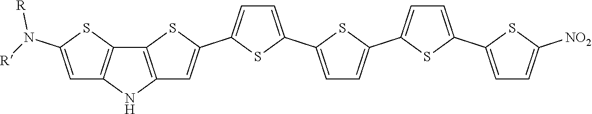
- non-limiting examples include 1,3,4-thiadiazole, quinoxaline, benzo[c][1,2,5]thiadiazole, 2H-benzo[d]imidazole, benzo[c][1,2,5]thiadiazole, thieno[3,4-b]pyrazine, [1,2,5]thiadiazolo[3,4-g]quinoxaline, pyrazino[2,3-g]quinoxaline, 5H-indeno[5,6-c][1,2,5]thiadiazole-5,7(6H)-dione, naphtho[1,2-c:5,6-c′]bis([1,2,5]thiadiazole), 4H-dithieno[3,2-b:2′, 3′-d]pyrrole, fluorene, carbazole, benzofuran, thieno[3,2-b]thiophene, thiazolo[5,4-d]thiazole, 4H-cyclopenta[2,1-b
- Heteroaryl monomers are ideal due to the electron delocalization of the aromatic system and the electron density provided by hetero atoms such as sulfur.
- hetero atoms such as sulfur.
- the inclusion of non-aromatic heterocycles and aromatic carbo cycles, even at positions within the oligomer not optimal for electronic gradient, can be tolerated and in many cases provides advantages in synthesis.
- the optimal monomers to be used in a specific oligomer are more electron-rich monomers that have a high HOMO value and more electron-poor monomers that have a relatively low LUMO value.
- terms like electron-rich and electron-poor are relative and what may be an electron-poor monomer in one oligomer may function as an electron-rich monomer in another, and vice-versa.
- the utilization of the electron affinity gradient and the low HOMO-LUMO band gap results in an oligomer with a high degree of polarizability, allowing for greater energy storage.
- the electron-donor and electron-acceptor groups further enhance the polarizability of the oligomer, especially when they are positioned on opposite sides of the oligomer such that the electron-donor(s) are on the side with higher electron affinity and the electron-acceptors are on the side with the lower electron affinity.
- These oligomeric dielectric materials can be described by the structural formula shown in FIG. 4 ,
- C is a linear chain oligomeric polarizable core with a system of conjugated multiple and single bonds wherein the oligomer chain possesses an electron affinity gradient, there is at least one electron-donor group, D, attached to the polarizable core, there is at least one electron-acceptor group, A, attached to the polarizable core, p′ and q′ represent the number of electron-donor and electron-acceptor groups present, respectively, and are any integer greater than zero, and at least one resistive insulating group is covalently attached to the molecular structure at any location.
- conjugate multiple bond as used herein may refer to conjugated double, triple or quadruple bonds.
- Placement of the electron-donor and electron-acceptor groups has some influence on their polarizability enhancement.
- Preferred embodiments place A and D on opposite, terminal monomers as described by the structural formula shown in FIG. 5 ,
- the linear oligomeric polarizable core is comprised of a plurality of similar or different cyclic monomers C 1 -C n , that are connected to each other by L′-L n-1 , each independently selected from possible linking groups that would retain a system of conjugated bonds throughout the oligomer, preferably single bonds, double bonds, —C ⁇ C—, —C ⁇ N—, —N ⁇ N—, and acetylene, at least one electron-donor group, D, attached to a terminal cyclic monomer on the more electron dense end of the linear polarizable core, at least one electron-withdrawing group, A, attached to a terminal cyclic monomer on the less electron dense end of the linear polarizable core, R, are resistive insulating group locations and at least one resistive insulating group is bound to the material at one of the resistive insulating group locations.
- the general structural formula includes an electron donating group at one end and an electron accepting group at the other end and six units in between the two ends.
- the six units include some combination involving standard units with either electron rich units, electron poor units, or both electron rich units and electron poor units.
- D is an electron donating group
- A is an electron accepting group. While these particular depictions are hexamers, other oligomer lengths are possible.
- the ‘standard unit’ depicted is typically a heteroaryl or carbocycle of average electron density, preferred embodiments include benzene, thiophene, selenophene, phosphole, benzothiophene, benzoselenophene, phosphindole, isophosphindole, dibenzothiophene, dibenzoselenophene, benzophosphindole, phosphinine, phosphinoline, and acridophosphine.
- the ‘electron poor unit’ in FIG. 1B is a heteroaryl of high electron density such as benzothiodiazole, benzoselenadiazole, thienopyrazine, and selenophenopyrazine.
- electron rich and electron poor are relative terms. It is possible for a “standard unit”, such as thiophene, for example, to function as the electron rich monomer when adjacent to sufficiently electron poor monomers. From these depictions it can be seen that electron-rich and electron-poor monomers may, but need not be, adjacent.
- the term gradient is not meant to necessitate that each successive monomer be more electron-rich or electron poor than the preceeding monomer. As long as the inclusion of an electron-rich or electron-poor monomer is incorporated in a manner that results in asymmetry within the oligomer the gradient as defined herein is achieved.
- A may be selected from —NO 2 , —CHO (aldehyde), —CRO (keto group), —SO 3 H (sulfonic acids), —SO 3 R (sulfonates), —SO 2 NH 2 , —SONRH, —SONR 2 (sulfonamides), —COOH (carboxylic acid), —COOR (esters, from carboxylic acid side), —CONH 2 , —CONHR, —CONR 2 (amides, from carboxylic acid side), —CF 3 , —CCl 3 , and —CN, and D may be selected from —NH 2 , —NHR, —NR 2 , —OH, OR (ethers), —NHCOR (amides, from amine side), —OCOR (esters, from alcohol side), alkyls, and —C 6 H 5 , vinyls, wherein R and R′ and R′′ are radicals selected from the list comprising hydrogen
- insulating resistive groups include hydrocarbon and halohydrocarbon chains, non-aromatic hydrocarbocycles, non-aromatic heterocycles, aryls, siloxanes, and/or polyethylene glycol linear or branched chains.
- rigid insulating resistive groups maybe non-aromatic carbocycles, non-aromatic heterocycles, and aryl groups.
- R and R′ can independently at all instances be any insulating resistive group, preferably alky, cycloalkyl, or aryl groups.
- a composite oligomer may be attached to a polymer.
- This is termed a “side-chain polymer” system.
- This system has the advantages over guest-host systems because high composite oligomer concentrations are incorporated into the polymer with high order and regularity and without phase separation or concentration gradients. These systems are cross-linked or non-cross-linked.
- a side-chain polymer maybe comprised of a polymeric backbone and a polarizable side-chain, wherein the polarizable side-chain is selected from composite oligomeric organic compounds described by the structural formula shown in FIG. 4 ,
- C is a linear chain oligomeric polarizable core with a system of conjugated multiple and single bonds wherein one end of the oligomer has greater electron density than the other end and, there is at least one electron-donor group, D, attached to the polarizable core, there is at least one electron-acceptor group, A, attached to the polarizable core, and p′ and q′ represent the number of electron-donor and electron-acceptor groups present, respectively, and are any integer greater than zero.
- the polymer must possess resistive insulating groups.
- resistive insulating groups may be within the backbone, may be used to connect the polarizable side-chain to the backbone, may be covalently attached to the polarizable side-chain, or may themselves be side-chains in a copolymer species.
- the polymer may be a homopolymer or a copolymer
- the insulating resistive groups may be attached to the metadielectric core or a separate sidechain.
- Core represents the conjugated oligomer with at least two different monomers to give an electronic gradient
- R is independently selected from hydrocarbon, halohydrocarbon, non-aromatic hydrocarbocycles, and non-aromatic heterocycles, which may be interrupted by hetero atoms
- D is independently selected from —O—, —C(O)O—, -Ak-O— or —C(O)OAk-, —NR—, —NH—R, —C(O)NH—, —C(O)NR—, -Ak-NH—, Ak-NR—
- Y is independently selected from 0 or NH or NAk, wherein Ak is any substituted or unsubstituted alkyl which may be interrupted by hetero atoms, n is 0-300, and m is 1-300.
- the composite polymer may include more than one type of insulating resistive groups. In another embodiment, the composite polymer comprises more than one type of ordered insulating resistive groups. In yet another embodiment, the composite polymer comprises at least one insulating resistive group or at least one type of ordered insulating resistive groups.
- a metadielectric film may include a polymer matrix and at least one oligomeric dielectric material.
- the metadielectric layer may be comprised of a mixture of oligomeric dielectric materials.
- the metadielectric layer maybe comprised of any organic composite oligomers, compounds, or polymers as disclosed in U.S. patent application Ser. No. 14/710,491 filed May 12, 2015, Ser. No. 15/043,186 filed Feb. 12, 2016, Ser. No. 15/043,209 filed Feb. 12, 2016, Ser. No. 15/194,224 filed Jun. 27, 2016, Ser. No. 15/043,247 filed Feb. 12, 2016, Ser. No. 15/090,509 filed Apr. 4, 2016, and Ser. No. 15/163,595 filed May 24, 2016 all of which are entirely incorporated herein.
- the polymer matrix may additionally include at least one monomer selected from acrylate, ester, and aramid.
- the film may include a plasticizer.
- non-ionic plasticizers can improve the metadielectric layer's resistivity through smoothing out electric field lines. This phenomenon occurs when the plasticizers fill voids and/or assists in supramolecular alignment. Additionally, plasticizers can improve the material's mechanical properties by reducing brittleness of the material during and post processing.
- the film may include a mixture of polyacrylate and polyamide materials. In some implementations of the above metadielectric film, the film may have a relative permittivity greater than or equal to 1000, a resistivity greater than or equal to 10 16 Ohm cm.
- metadielectric films of the type described herein may be used in metacapacitors.
- a metacapacitor according to certain aspects of the present disclosure may include a first electrode, a second electrode, and a metadielectric film, e.g., as described generally above or in further detail below, sandwiched between said first and second electrodes.
- such a metacapacitor may be characterized by a capacitance that varies non-linearly with voltage.
- one or more of the electrodes may be formed on a substrate of flexible tape, wherein the substrate, first and second electrodes, and the metadielectric film are coiled such that the substrate forms an isolation layer between the first and second electrodes, and wherein the substrate is selected metallic and plastic films.
- FIG. 1B illustrates an example of a metacapacitor comprising a first electrode 1 , a second electrode 2 , and a metadielectric layer 3 disposed between said first and second electrodes as shown in FIG. 1B .
- the electrodes 1 and 2 may be made of a metal, such as copper, zinc, or aluminum or other conductive material such as graphite or carbon nanomaterials and are generally planar in shape.
- the electrodes 1 , 2 may be flat and planar and positioned parallel to each other.
- the electrodes may be planar and parallel, but not necessarily flat, they may be coiled, rolled, bent, folded, or otherwise shaped to form the capacitor. It is also possible for the electrodes to be non-flat, non-planar, or non-parallel or some combination of two or more of these.
- a spacing d between the electrodes land 2 may range from about 3 nm to about 100 ⁇ m.
- the metacapacitor may have an insulation layer to insulate electrodes 1 and 2 from making ohmic contact with each other in coiled, rolled, bent, and folded embodiments.
- the insulation layer include metadielectric material, polypropylene (PP), polyethylene terephthalate polyester (PET), polyphenylene sulfide (PPS), polyethylene naphthalate (PEN), polycarbonate (PP), polystyrene (PS), and polytetrafluoroethylene (PTFE).
- the electrodes 1 and 2 may have the same shape as each other, the same dimensions, and the same area A.
- the area A of each electrode 1 and 2 may range from about 0.01 m 2 to about 1000 m 2 .
- the energy storage capacity U is determined by the dielectric constant ⁇ , the area A, the electrode spacing d, and the breakdown field E bd .
- a capacitor or capacitor bank may be designed to have any desired energy storage capacity U.
- a capacitor in accordance with aspects of the present disclosure may have an energy storage capacity U ranging from about 500 Joules to about 2 ⁇ 10 16 Joules.
- a capacitor of the type described herein may have a specific energy capacity per unit mass ranging from about 10 W ⁇ h/kg up to about 100,000 W ⁇ h/kg, though implementations are not so limited.
- electrodes 1 and 2 may have different shapes from each other with the same or different dimensions, and the same or different areas.
- the present disclosure includes metacapacitors that are coiled, e.g., as depicted in FIGS. 2A, 2B and 3 .
- electrodes 19 , 21 e.g., metal electrodes
- margin portions 18 , 20 that are free of metal located on opposite edges of the metadielectric layer 17 .
- an electrically insulating layer 15 e.g., a plastic material is formed over one of the electrodes 21 or a plastic film is overlaid on one of the electrodes 21 .
- the electrically insulating layer 15 may include metadielectric materials or common capacitor insulating materials such as PET.
- the metadielectric lay 17 may be formed, e.g., by applying a solution containing oligomeric dielectric material to the electrode 19 and then drying the applied solution to form a solid layer of the oligomeric dielectric material.
- electrodes 19 and 21 may be formed onto opposite surfaces of an insulating layer 15 with margin portions 18 , 20 that are free of electrode material located on opposite edges of the insulating layer 15 .
- a configuration of electrodes 19 , 21 and insulating layer 15 form a tape or a multilayered tape.
- the electrically insulating layer 15 may include metadielectric materials or common capacitor insulating materials such as PET.
- the metadielectric lay 17 may be formed, e.g., by applying a solution containing oligomeric dielectric material to the electrode 19 and then drying the applied solution to form a solid layer of the oligomeric dielectric material.
- the thickness of the metadielectric layer may be a relatively uniformly thick layer.
- the metadielectric layer thickness may range from 0.01 ⁇ m to 50 ⁇ m depending on the desired maximum capacitor voltage. In general, thicker metadielectric layers are used for higher maximum capacitor voltages. Furthermore, with a given metacapcitor the metadielectric layer thickness may vary due to normal manufacturing process variations, e.g., by about 1% to 10% of a nominal thickness value.
- the first metal electrode 19 is formed on a portion of a first surface of the metadielectric layer 17 with a first margin portion 18 that is free of metal.
- the second electrode 21 is formed on a portion of a second surface of the plastic layer with a second margin portion 20 located on an opposite edge of the metadielectric layer 17 being free of metal.
- the multilayered structure depicted in FIG. 2A may be wound into a coil as shown in FIG. 2B .
- the insulating layer 15 prevents undesired electrical shorts between the first and second electrodes after being wound into the coil.
- the insulating layer 15 may include a metadielectric material, polypropylene (PP), polyethylene terephthalate polyester (PET), polyphenylene sulfide (PPS), polyethylene naphthalate (PEN), polycarbonate (PP), polystyrene (PS), or polytetrafluoroethylene (PTFE).
- PP polypropylene
- PET polyethylene terephthalate polyester
- PPS polyphenylene sulfide
- PEN polyethylene naphthalate
- PP polycarbonate
- PS polystyrene
- PTFE polytetrafluoroethylene
- a metacapacitor 22 comprises a first electrode 23 , a second electrode 25 , and a metadielectric material layer 24 of the type described herein disposed between said first and second electrodes.
- the electrodes 23 and 25 may be made of a metal, such as copper, zinc, or aluminum or other conductive material such as graphite or carbon nanomaterials and are generally planar in shape.
- the electrodes and metadielectric material layer 24 are in the form of long strips of material that are sandwiched together and wound into a coil along with an insulating material 26 , e.g., a plastic film such as polypropylene or polyester to prevent electrical shorting between the electrodes 23 and 25 .
- the insulating material may include a metadielectric layer comprised of any composite oligomer or polymer formed therefrom or mixture thereof, as described herein below.
- the electrodes may be multilayered structures consisting of a conductive layer and any combination of one or more of layers selected from the list of field planarization layer, surface planarization layer, electron blocking layer, and hole blocking layer.
- a metacapacitor may have a sequence (E-B1-D2-B2-E-B1-D2) m , wherein E are electrodes, B1 and B2 are respectively a hole blocking layer and electron blocking layer (or vice versa), D1 is a metadielectric layer, D2 is selected from a metadielectric layer or a plastic isolation layer (i.e. polypropylene), and m is an integer greater than or equal to 1.
- E electrodes
- B1 and B2 are respectively a hole blocking layer and electron blocking layer (or vice versa)
- D1 is a metadielectric layer
- D2 is selected from a metadielectric layer or a plastic isolation layer (i.e. polypropylene)
- m is an integer greater than or equal to 1.
- Non-limiting examples of suitable coiled capacitors are described in U.S. patent application Ser. No. 14/752,600 which is herein incorporated by reference in their entirety.
- the present invention provides a coiled capacitor comprising a coil formed by a flexible multilayered tape, and a first terminating electrode (a first contact layer) and a second terminating electrode (a second contact layer) which are located on butts of the coil.
- the flexible multilayered tape contains the following sequence of layers: first metal layer, a layer of a plastic, second metal layer, a layer of energy storage material.
- the first metal layer forms an ohmic contact with the first terminating electrode (the first contact layer) and the second metal layer (the second contact layer) forms an ohmic contact with the second terminating electrode.
- the layer of energy storage material may be any oligomer or polymer described herein.
- a liquid or solid composite oligomer is placed between the first and second electrodes.
- a solid is, for example, pressed into a pellet and placed between the first electrode and the second electrode.
- the solid can be ground into a powder before pressing.
- At least one type of oligomeric dielectric material may be dissolved or suspended in a solvent.
- the resultant material can be spin coated, extruded via slot die, roll-to-roll coated, or pulled and dried to form a dielectric film.
- a composite oligomer may be dissolved or suspended in a polymer.
- This is termed a “guest-host” system where the oligomer is the guest and the polymer is the host.
- Polymer hosts include, but are not limited to, poly(methyl methacrylate), polyimides, polycarbonates and poly( ⁇ -caprolactone). These systems are cross-linked or non-cross-linked.
- the insulating resistive groups may also crosslink to further enhance the structure of the dielectric film which can reduce localized film defects and enhance the film's breakdown voltage or breakdown field.
- a polymer of a composite non-linear polarizable compound and electrically resistive chain may crosslink inter- and/or intra polymer backbones to enhance the dielectric film structure, which can reduce localized film defects and enhance the film's breakdown voltage or breakdown field.
- ordered insulating resistive groups can improve solubility of the composite compound in organic solvents.
- the insulating resistive groups can act to hinder electro-polar interactions between supramolecular structures formed from pi-pi stacking of the optionally attached polycyclic conjugated molecule. Even further, the insulating resistive groups can act to hinder electro-polar interaction between repeat units of a polymer consisting of non-linear polarizable compounds.
- An oligomer consisting of a monomer with a non-linear polarizable compound and an insulating resistive group substituent can be used to introduce some order to dielectric films consisting of said oligomer due to the insulating resistive group and non-linear polarizable compounds forming polar, pi-pi, van der Waals interaction, or any combination thereof.
- composite oligomers may be embedded in matrices such as oxides, halides, salts and organic glasses.
- matrices such as oxides, halides, salts and organic glasses.
- An example of a matrix is inorganic glasses comprising the oxides of aluminum, boron, silicon, titanium, vanadium and zirconium.
- the composite oligomers that make up a dielectric oligomeric dielectric material may be aligned, partially aligned or unaligned.
- the composite oligomer is preferably aligned for optimal geometric configuration of polarizing units as this results in higher capacitance values in the capacitor.
- One method of alignment is to apply a DC electric field to the composite oligomer at a temperature at which the polarizable units can be oriented. This method is termed “poling.” Poling is generally performed near the glass transition temperature of polymeric and glassy systems.
- One possible method of poling is corona poling.
- Other methods of alignment could be roll-to-roll, Meyer bar, dip, slot die, and air knife coating of solutions and liquid crystal solutions of said side-chain polymers or composite oligomers.
- the side-chain polymer or composite oligomers may form liquid crystals in solution or solvent and with or without external influence.
- liquid crystals include lyotropic and thermotropic liquid crystals.
- external influences include heat, electric field, mechanical disturbances (e.g. vibration or sonication), and electromagnetic radiation.
- Said liquid crystals are supramolecular structures comprised of said side-chain polymers or composite oligomer in solution or solvent and are ordered and aligned or partially ordered or partially aligned.
- Such liquid crystal materials may be coated onto a substrate, e.g., by roll-to-roll, Meyer bar, dip, slot die, or air knife coating in a process that includes mechanical ordering of the liquid crystals, and drying of the liquid crystal solution or evaporation of the solvent such that the liquid crystals form a crystalline or semi-crystalline layer or film of metadielectric material.
- such liquid crystal materials may be extruded as a film such that the liquid crystals form a crystalline or semi-crystalline film of metadielectric material.
- extrusion of such liquid crystal materials may be coextruded as a multilayer film.
- Such multilayer films may include alternating layers of conducting layers and insulating layers, wherein the insulating layers may be the aforementioned crystalline or semi-crystalline layer of metadielectric material.
- Preferred polymer embodiments are polyester, polyalkylacrylate (preferably methacrylic and acrylic), polyamide, and polyaramid.
- This insulating resistive group may be attached to the polarizable side chain or may be its own independent side chain interspersed in any pattern or random assortment with the polarizable side chains or a mixture thereof.
- These species can be represented by one of the following formula.
Landscapes
- Engineering & Computer Science (AREA)
- Power Engineering (AREA)
- Chemical & Material Sciences (AREA)
- Polymers & Plastics (AREA)
- Health & Medical Sciences (AREA)
- Organic Chemistry (AREA)
- Medicinal Chemistry (AREA)
- Chemical Kinetics & Catalysis (AREA)
- Manufacturing & Machinery (AREA)
- Microelectronics & Electronic Packaging (AREA)
- Fixed Capacitors And Capacitor Manufacturing Machines (AREA)
- Compositions Of Macromolecular Compounds (AREA)
- Organic Insulating Materials (AREA)
- Heterocyclic Carbon Compounds Containing A Hetero Ring Having Oxygen Or Sulfur (AREA)
- Nitrogen And Oxygen Or Sulfur-Condensed Heterocyclic Ring Systems (AREA)
- Inorganic Insulating Materials (AREA)
Abstract
- wherein C is a linear chain oligomeric polarizable core with a system of conjugated multiple and single bonds wherein the linear chain oligomeric polarizable core possesses at least two different monomers with differing electron affinity, and the different monomers are positioned within the linear chain oligomeric polarizable core such that an electron affinity gradient is present, and the differing monomers have a low HOMO-LUMO bandgap between them, and there is at least one electron-donor group, D, attached to the linear chain oligomeric polarizable core, there is at least one electron-acceptor group, A, is attached to the linear chain oligomeric polarizable core, p′ and q′ represent the number of electron-donor and electron-acceptor groups present, respectively, and are any integer greater than zero, and at least one resistive insulating group is covalently attached to the molecular structure at any location.
Description
| TABLE A |
| MONOMERS |
| A |
|
||
| B |
 |
||
| C |
 |
||
| D |
|
||
| E |
|
||
| F |
|
||
| G |
 |
||
| H |
 |
||
| I |
|
||
| J |
 |
||
| K |
 |
||
| L |
 |
||
| M |
 |
||
| N |
 |
||
| O |
 |
||
| P |
 |
||
| Q |
|
||
| R |
|
||
| S |
 |
||
| T |
 |
||
| U |
 |
||
| V |
 |
||
| W |
 |
||
| X |
 |
||
| Y |
 |
||
| Z |
 |
||
| AA |
 |
||
| BB |
 |
||
| CC |
 |
||
| DD |
 |
||
| EE |
 |
||
| FF |
 |
||
To better demonstrate the concept of electron affinity gradient, the following depictions show how monomers of differing electron affinity can be incorporated into hexamers to result in oligomers with asymmetric electron affinity as shown in
In
| TABLE 1 |
| Examples of Composite Oligomeric Dielectric Organic Material Compounds |
| Oligomer | No. |
 | 1 |
 | 2 |
 | 3 |
 | 4 |
 | 5 |
 | 6 |
 | 7 |
 | 8 |
 | 9 |
 | 10 |
 | 11 |
 | 12 |
 | 13 |
 | 14 |
 | 15 |
 | 16 |
 | 17 |
 | 18 |
 | 19 |
 | 20 |
 | 21 |
 | 22 |
 | 23 |
 | 24 |
 | 25 |
 | 26 |
 | 27 |
 | 28 |
 | 29 |
 | 30 |
 | 31 |
 | 32 |
 | 33 |
 | 34 |
 | 35 |
 | 36 |
Where R and R′ can independently at all instances be any insulating resistive group, preferably alky, cycloalkyl, or aryl groups.
| TABLE 2 |
| Exemplary Homo-polymer and Copolymers |
 |
37 |
 |
38 |
 |
39 |
 |
40 |
 |
41 |
 |
42 |
 |
43 |
 |
44 |
 |
45 |
 |
46 |
 |
47 |
 |
48 |
 |
49 |
 |
50 |
 |
51 |
 |
52 |
 |
53 |
 |
54 |
 |
55 |
 |
56 |
 |
57 |
C=εε o A/d, (I)
where ε0 is the permittivity of free space (8.85×10⁻¹² Coulombs2/(Newton·meter2)) and ε is the dielectric constant of the dielectric layer. The energy storage capacity U of the capacitor may be approximated as:
U=½εεo AE bd 2 d (II)
Claims (13)


Priority Applications (7)
| Application Number | Priority Date | Filing Date | Title |
|---|---|---|---|
| US15/844,364 US10403435B2 (en) | 2017-12-15 | 2017-12-15 | Edder compound and capacitor thereof |
| EP18887738.5A EP3724185A1 (en) | 2017-12-15 | 2018-12-14 | Oligomeric dielectric materials and capacitor thereof |
| CN201880089440.5A CN111801326A (en) | 2017-12-15 | 2018-12-14 | Oligomeric Dielectric Materials and Their Capacitors |
| PCT/US2018/065840 WO2019118922A1 (en) | 2017-12-15 | 2018-12-14 | Oligomeric dielectric materials and capacitor thereof |
| JP2020533026A JP2021507886A (en) | 2017-12-15 | 2018-12-14 | Oligomer dielectric material and its capacitors |
| CA3085341A CA3085341A1 (en) | 2017-12-15 | 2018-12-14 | Oligomeric dielectric materials and capacitor thereof |
| US16/509,956 US10910159B2 (en) | 2017-12-15 | 2019-07-12 | Edder compound and capacitor thereof |
Applications Claiming Priority (1)
| Application Number | Priority Date | Filing Date | Title |
|---|---|---|---|
| US15/844,364 US10403435B2 (en) | 2017-12-15 | 2017-12-15 | Edder compound and capacitor thereof |
Related Child Applications (1)
| Application Number | Title | Priority Date | Filing Date |
|---|---|---|---|
| US16/509,956 Continuation US10910159B2 (en) | 2017-12-15 | 2019-07-12 | Edder compound and capacitor thereof |
Publications (2)
| Publication Number | Publication Date |
|---|---|
| US20190189347A1 US20190189347A1 (en) | 2019-06-20 |
| US10403435B2 true US10403435B2 (en) | 2019-09-03 |
Family
ID=66814672
Family Applications (2)
| Application Number | Title | Priority Date | Filing Date |
|---|---|---|---|
| US15/844,364 Active US10403435B2 (en) | 2017-12-15 | 2017-12-15 | Edder compound and capacitor thereof |
| US16/509,956 Expired - Fee Related US10910159B2 (en) | 2017-12-15 | 2019-07-12 | Edder compound and capacitor thereof |
Family Applications After (1)
| Application Number | Title | Priority Date | Filing Date |
|---|---|---|---|
| US16/509,956 Expired - Fee Related US10910159B2 (en) | 2017-12-15 | 2019-07-12 | Edder compound and capacitor thereof |
Country Status (6)
| Country | Link |
|---|---|
| US (2) | US10403435B2 (en) |
| EP (1) | EP3724185A1 (en) |
| JP (1) | JP2021507886A (en) |
| CN (1) | CN111801326A (en) |
| CA (1) | CA3085341A1 (en) |
| WO (1) | WO2019118922A1 (en) |
Cited By (1)
| Publication number | Priority date | Publication date | Assignee | Title |
|---|---|---|---|---|
| US10910159B2 (en) * | 2017-12-15 | 2021-02-02 | Capacitor Sciences Incorporated | Edder compound and capacitor thereof |
Citations (100)
| Publication number | Priority date | Publication date | Assignee | Title |
|---|---|---|---|---|
| US5717733A (en) | 1995-05-31 | 1998-02-10 | Quanta Vision, Inc. | X-ray and neutron diffractometric imaging of the internal structure of objects |
| US5805662A (en) | 1994-12-08 | 1998-09-08 | Quanta Vision, Inc. | Using deflected penetrating radiation to image an object's internal structure |
| US6049428A (en) | 1994-11-18 | 2000-04-11 | Optiva, Inc. | Dichroic light polarizers |
| US6054712A (en) | 1998-01-23 | 2000-04-25 | Quanta Vision, Inc. | Inspection equipment using small-angle topography in determining an object's internal structure and composition |
| US6175117B1 (en) | 1998-01-23 | 2001-01-16 | Quanta Vision, Inc. | Tissue analysis apparatus |
| US6281503B1 (en) | 1998-05-06 | 2001-08-28 | Quanta Vision, Inc. | Non-invasive composition analysis |
| US20010029638A1 (en) | 2000-02-25 | 2001-10-18 | Bobrov Yuri A. | Dichroic polarizer and material |
| US6399166B1 (en) | 1996-04-15 | 2002-06-04 | Optiva, Inc. | Liquid crystal display and method |
| US20020090188A1 (en) | 2000-11-14 | 2002-07-11 | Optiva, Inc. | Optical waveguides and method of fabrication thereof |
| US20020093611A1 (en) | 2001-01-10 | 2002-07-18 | Lazarev Pavel I. | Device and method for forming anisotropic films |
| US20020105608A1 (en) | 2000-12-06 | 2002-08-08 | Lazarev Pavel I. | Liquid crystal information displays |
| US6483891B1 (en) | 1998-09-17 | 2002-11-19 | Quanta Vision, Inc. | Reduced-angle mammography device and variants |
| US20030071939A1 (en) | 2001-09-21 | 2003-04-17 | Lazarev Pavel I. | Liquid crystal display with reflecting polarizer |
| US6563640B1 (en) | 1998-10-28 | 2003-05-13 | Optiva, Inc. | Dichroic polarizer and method for making the same |
| US20030148196A1 (en) | 2002-02-06 | 2003-08-07 | Lazarev Pavel I. | Method of fabrication anisotropic crystal film on a receptor plate via transfer from the donor plate, the donor plate and the method of fabrication |
| US20030154909A1 (en) | 2001-02-07 | 2003-08-21 | Lazarev Pavel I. | Method of obtaining anisotropic crystalline films and devices for implementation of the method |
| US20030161022A1 (en) | 2001-11-19 | 2003-08-28 | Optiva, Inc. | Electrooptical devices, electrooptical thin crystal films and methods making same |
| US6619553B1 (en) | 1999-03-01 | 2003-09-16 | Optiva, Inc. | Interactive smart card and method of its fabrication |
| US20040028839A1 (en) | 2002-08-07 | 2004-02-12 | Paukshto Michael V. | Optical anisotropic film |
| US20040036817A1 (en) | 2002-08-22 | 2004-02-26 | Paukshto Michael V. | Display panel and multilayer plates for production of this display panel |
| US20040067324A1 (en) | 2002-09-13 | 2004-04-08 | Lazarev Pavel I | Organic photosensitive optoelectronic device |
| US20040070704A1 (en) | 2001-10-02 | 2004-04-15 | Lazarev Pavel I. | Multilayer plate for the fabrication of a display panel |
| US20040142183A1 (en) | 2003-01-17 | 2004-07-22 | Lazarev Pavel I. | Anisotropic film manufacturing |
| US20040214986A1 (en) | 2003-04-22 | 2004-10-28 | Lazarev Pavel I. | Two-phase polymeric materials and methods for making |
| US20040224182A1 (en) | 2003-01-07 | 2004-11-11 | Lazarev Pavel I. | Backlight polar organic light-emitting device |
| US20040233528A1 (en) | 2001-07-10 | 2004-11-25 | Lazarev Pavel I | Multilayer optical coating |
| US20040233351A1 (en) | 2001-07-26 | 2004-11-25 | Lazarev Pavel I | Liquid crystal display and the method of its fabrication |
| US6831964B1 (en) | 1999-02-17 | 2004-12-14 | Quanta Vision, Inc. | Stot-type high-intensity X-ray source |
| US20050052859A1 (en) | 2003-07-25 | 2005-03-10 | Lazarev Pavel I. | Anisotropic fluorescent thin crystal film and backlight system and liquid crystal display incorporating the same |
| US20050104037A1 (en) | 2003-09-23 | 2005-05-19 | Lazarev Pavel I. | Two-phase film materials and method for making |
| US20050104027A1 (en) | 2003-10-17 | 2005-05-19 | Lazarev Pavel I. | Three-dimensional integrated circuit with integrated heat sinks |
| US20050103258A1 (en) | 2003-09-24 | 2005-05-19 | Lazarev Pavel I. | Epitaxial organic layered structure and method for making |
| US20050136345A1 (en) | 2003-12-18 | 2005-06-23 | Lazarev Pavel I. | Method and device for transferring anisotropic crystal film from donor to receptor, and the donor |
| US20050146671A1 (en) | 2003-12-24 | 2005-07-07 | Khavrounyak Igor V. | Method of manufacturing thin crystal films |
| US20050194640A1 (en) | 2003-10-17 | 2005-09-08 | Lazarev Pavel I. | Organic thin-film transistor |
| US20050196550A1 (en) | 2004-03-02 | 2005-09-08 | Lazarev Pavel I. | Compensator for liquid crystal display |
| US20050195340A1 (en) | 2004-03-04 | 2005-09-08 | Lazarev Pavel I. | Polarized interference recycling backlight module and liquid crystal display incorporating the same |
| US6942925B1 (en) | 1997-08-11 | 2005-09-13 | Optiva, Inc. | Dichroic polarizer |
| US20050200771A1 (en) | 2004-03-09 | 2005-09-15 | Lazarev Pavel I. | LCD comprising backlight and reflective polarizer on front panel |
| US20050212993A1 (en) | 2004-03-26 | 2005-09-29 | Lazarev Pavel I | Liquid crystal display panel with improved image contrast |
| US20050231661A1 (en) | 2004-04-15 | 2005-10-20 | Lazarev Pavel I | Non-absorbing polarization color filter and liquid crystal display incorporating the same |
| US20050253983A1 (en) | 2003-11-21 | 2005-11-17 | Carson Travis D | Materials and methods for the preparation of anisotropically-ordered solids |
| US20050271878A1 (en) | 2004-06-08 | 2005-12-08 | Optiva, Inc. | Supramolecular composite film material and method for fabricating |
| US20050286128A1 (en) | 2004-06-24 | 2005-12-29 | Optiva, Inc. | Biaxial crystal filter for viewing devices |
| US7015990B2 (en) | 2000-04-24 | 2006-03-21 | Nitto Denko Corporation | Liquid crystal display including O-type and E-type polarizer |
| US7019453B2 (en) | 2000-08-17 | 2006-03-28 | Lumera Corporation | Polymers having pendant nonlinear optical chromophores and electro-optic devices therefrom |
| US20060065888A1 (en) | 2004-09-27 | 2006-03-30 | Lazarev Pavel I | Organic semiconductor diode |
| US7206111B2 (en) | 2000-08-17 | 2007-04-17 | Lumera Corporation | Sterically hindered PI-bridge nonlinear optical chromophores, processes including same, and devices therefrom |
| US20070195416A1 (en) | 2003-08-07 | 2007-08-23 | Nitto Denko Corporation | Interferential Optical Filter |
| US20090034073A1 (en) | 2006-01-23 | 2009-02-05 | Crysoptix Kk | Multilayer Polarizer |
| US20090161037A1 (en) | 2006-04-13 | 2009-06-25 | Crysoptix Kk | Backlight Module and Liquid Crystal Display Incorporating the Same |
| US20090191394A1 (en) | 2005-10-07 | 2009-07-30 | Lazarev Pavel I | Oarganic Compound, Optical Crystal Film and Method of Production Thereof |
| US20100039705A1 (en) | 2006-01-13 | 2010-02-18 | Crysoptix Kk | Organic Compound, Anisotropic Optical Film and Method of Production Thereof |
| US20100038629A1 (en) | 2006-11-06 | 2010-02-18 | Carben Semicon Limited | Anisotropic Semiconductor Film and Method of Production Thereof |
| US20100047477A1 (en) | 2006-01-13 | 2010-02-25 | Crysoptix Kk | 6,7-Dihydrobenzimidazo[1,2-c]Quinazolin-6-One Carboxylic Acids, their Esters, and Methods of Synthesis Thereof |
| US20100065122A1 (en) | 2006-09-26 | 2010-03-18 | Cryscade Solar Limited | Organic Compound, Photovoltaic Layer and Organic Photovoltaic Device |
| US20100173134A1 (en) | 2008-06-26 | 2010-07-08 | Carben Semicon Limited | Film and Device Using Layer Based on Ribtan Material |
| US20100224998A1 (en) | 2008-06-26 | 2010-09-09 | Carben Semicon Limited | Integrated Circuit with Ribtan Interconnects |
| US20100233491A1 (en) | 2006-08-16 | 2010-09-16 | Crysoptix Kk | Anisotropic Polymeric Film and Method of Production Thereof |
| US20100279122A1 (en) | 2006-08-16 | 2010-11-04 | Crysoptix Kk | Benzimidazole, Benzoxazole and Benzothiazole Derivatives, Optical Film Comprising them and Method of Producing thereof |
| US20110042649A1 (en) | 2008-02-15 | 2011-02-24 | Carben Semicon Limited | Thin-Film Transistor, Carbon-Based Layer and Method of Producing Thereof |
| US20110064892A1 (en) | 2008-03-04 | 2011-03-17 | Crysoptix Kk | Polycyclic Organic Compounds, Retardation Layer and Compensation Panel on Their Base |
| US20110149206A1 (en) | 2009-12-07 | 2011-06-23 | Crysoptix Kk | Polarizer and Liquid Crystal Display Comprising the Same |
| US20110149393A1 (en) | 2008-03-04 | 2011-06-23 | Crysoptic KK | Polycyclic Organic Compounds, Polarizing Elements and Method of Production Thereof |
| US8085370B2 (en) | 2005-05-20 | 2011-12-27 | Nemoptic | Single-polarizer reflective bistable twisted nematic (BTN) liquid crystal display device |
| US20120081784A1 (en) | 2010-10-02 | 2012-04-05 | Crysoptix Kk | Patterned retarder |
| US20120099052A1 (en) | 2010-10-21 | 2012-04-26 | Crysoptix Kk | Retarder and liquid crystal display comprising the same |
| US20120113380A1 (en) | 2010-11-09 | 2012-05-10 | Crysoptix Kk | Negative dispersion retardation plate and achromatic circular polarizer |
| US20120227802A1 (en) | 2011-03-10 | 2012-09-13 | Cryscade Solar Limited | Organic compound and photovoltaic device comprising the same |
| US20130003178A1 (en) | 2011-06-30 | 2013-01-03 | Crysoptix Kk | Three-dimensional circular polarization eyeglasses |
| US20160020027A1 (en) | 2014-05-12 | 2016-01-21 | Capacitor Sciences Incorporated | Capacitor and Method of Production Thereof |
| US20160020026A1 (en) | 2014-05-12 | 2016-01-21 | Capacitor Sciences Incorporated | Energy Storage Device and Method of Production Thereof |
| US20160196929A1 (en) | 2013-08-15 | 2016-07-07 | The Regents Of The University Of California | A multicomponent approach to enhance stability and capacitance in polymer-hybrid supercapacitors |
| US20160254092A1 (en) | 2015-02-26 | 2016-09-01 | Capacitor Sciences Incorporated | Self-healing capacitor and methods of production thereof |
| US20160314901A1 (en) | 2014-11-04 | 2016-10-27 | Capacitor Sciences Incorporated | Energy storage devices and methods of production thereof |
| US20160340368A1 (en) | 2015-05-21 | 2016-11-24 | Capacitor Sciences Incorporated | Energy storage molecular material, crystal dielectric layer and capacitor |
| US20160379757A1 (en) | 2015-06-26 | 2016-12-29 | Capacitor Sciences Incorporated | Coiled capacitor |
| US20170014900A1 (en) | 2014-04-25 | 2017-01-19 | Keihin Corporation | Squeeze pin circuit for die casting and hydraulic unit |
| US20170117097A1 (en) | 2015-10-21 | 2017-04-27 | Capacitor Sciences Incorporated | Organic compound, crystal dielectric layer and capacitor |
| US20170236641A1 (en) | 2016-02-12 | 2017-08-17 | Capacitor Sciences Incorporated | Furuta co-polymer and capacitor |
| US20170237274A1 (en) | 2016-02-12 | 2017-08-17 | Capacitor Sciences Incorporated | Grid capacitive power storage system |
| US20170233528A1 (en) | 2016-02-12 | 2017-08-17 | Capacitor Sciences Incorporated | Sharp polymer and capacitor |
| US20170237271A1 (en) | 2016-02-12 | 2017-08-17 | Capacitor Sciences Incorporated | Energy storage cell, capacitive energy storage module, and capacitive energy storage system |
| US20170236648A1 (en) | 2016-02-12 | 2017-08-17 | Capacitor Sciences Incorporated | Grid capacitive power storage system |
| US20170236642A1 (en) | 2016-02-12 | 2017-08-17 | Capacitor Sciences Incorporated | para-FURUTA POLYMER AND CAPACITOR |
| US20170232853A1 (en) | 2016-02-12 | 2017-08-17 | Capacitor Sciences Incorporated | Electric vehicle powered by capacitive energy storage modules |
| US20170287638A1 (en) | 2016-04-04 | 2017-10-05 | Capacitor Sciences Incorporated | Electro-polarizable compound and capacitor |
| US20170287637A1 (en) | 2016-04-04 | 2017-10-05 | Capacitor Sciences Incorporated | Electro-polarizable compound and capacitor |
| US20170283618A1 (en) | 2016-04-04 | 2017-10-05 | Capacitor Sciences Incorporated | Non-linear dielectric materials and capacitor |
| US20170301467A1 (en) | 2015-05-12 | 2017-10-19 | Capacitor Sciences Incorporated | Capacitor and method of production thereof |
| US20170301477A1 (en) | 2016-04-04 | 2017-10-19 | Capacitor Sciences Incorporated | Electro-polarizable compound and capacitor |
| US20170372842A1 (en) | 2016-06-27 | 2017-12-28 | Capacitor Sciences Incorporated | Electro-polarizable complex compound and capacitor |
| US20180033554A1 (en) | 2014-05-12 | 2018-02-01 | Capacitor Sciences Incorporated | Yanli dielectric materials and capacitor thereof |
| US20180061582A1 (en) | 2016-02-12 | 2018-03-01 | Capcitor Sciences Incorporated | Furuta and para-furuta polymer formulations and capacitors |
| US20180114641A1 (en) | 2014-05-12 | 2018-04-26 | Capacitor Sciences Incorporated | Solid multilayer structure as semiproduct for meta-capacitor |
| US20180137984A1 (en) | 2015-05-21 | 2018-05-17 | Capacitor Sciences Incorporated | Solid state energy storage device |
| US20180137978A1 (en) | 2016-04-04 | 2018-05-17 | Capacitor Sciences Incorporated | Hein electro-polarizable compound and capacitor thereof |
| US20180158616A1 (en) | 2016-12-02 | 2018-06-07 | Capacitor Sciences Incorporated | Multilayered electrode and film energy storage device |
| US20180205242A1 (en) | 2016-02-12 | 2018-07-19 | Capacitor Sciences Incorporated | Capacitor based power system and unmanned vehicle with the capacitor based power system thereof |
| US10163575B1 (en) | 2017-11-07 | 2018-12-25 | Capacitor Sciences Incorporated | Non-linear capacitor and energy storage device comprising thereof |
Family Cites Families (2)
| Publication number | Priority date | Publication date | Assignee | Title |
|---|---|---|---|---|
| DE102010048498A1 (en) * | 2010-10-14 | 2012-04-19 | Merck Patent Gmbh | Materials for organic electroluminescent devices |
| US10403435B2 (en) * | 2017-12-15 | 2019-09-03 | Capacitor Sciences Incorporated | Edder compound and capacitor thereof |
-
2017
- 2017-12-15 US US15/844,364 patent/US10403435B2/en active Active
-
2018
- 2018-12-14 WO PCT/US2018/065840 patent/WO2019118922A1/en not_active Ceased
- 2018-12-14 CN CN201880089440.5A patent/CN111801326A/en active Pending
- 2018-12-14 EP EP18887738.5A patent/EP3724185A1/en not_active Withdrawn
- 2018-12-14 JP JP2020533026A patent/JP2021507886A/en active Pending
- 2018-12-14 CA CA3085341A patent/CA3085341A1/en not_active Abandoned
-
2019
- 2019-07-12 US US16/509,956 patent/US10910159B2/en not_active Expired - Fee Related
Patent Citations (166)
| Publication number | Priority date | Publication date | Assignee | Title |
|---|---|---|---|---|
| US6049428A (en) | 1994-11-18 | 2000-04-11 | Optiva, Inc. | Dichroic light polarizers |
| US5805662A (en) | 1994-12-08 | 1998-09-08 | Quanta Vision, Inc. | Using deflected penetrating radiation to image an object's internal structure |
| US5717733A (en) | 1995-05-31 | 1998-02-10 | Quanta Vision, Inc. | X-ray and neutron diffractometric imaging of the internal structure of objects |
| US6399166B1 (en) | 1996-04-15 | 2002-06-04 | Optiva, Inc. | Liquid crystal display and method |
| US6942925B1 (en) | 1997-08-11 | 2005-09-13 | Optiva, Inc. | Dichroic polarizer |
| US6054712A (en) | 1998-01-23 | 2000-04-25 | Quanta Vision, Inc. | Inspection equipment using small-angle topography in determining an object's internal structure and composition |
| US6175117B1 (en) | 1998-01-23 | 2001-01-16 | Quanta Vision, Inc. | Tissue analysis apparatus |
| US6281503B1 (en) | 1998-05-06 | 2001-08-28 | Quanta Vision, Inc. | Non-invasive composition analysis |
| US6483891B1 (en) | 1998-09-17 | 2002-11-19 | Quanta Vision, Inc. | Reduced-angle mammography device and variants |
| US6563640B1 (en) | 1998-10-28 | 2003-05-13 | Optiva, Inc. | Dichroic polarizer and method for making the same |
| US6831964B1 (en) | 1999-02-17 | 2004-12-14 | Quanta Vision, Inc. | Stot-type high-intensity X-ray source |
| US6619553B1 (en) | 1999-03-01 | 2003-09-16 | Optiva, Inc. | Interactive smart card and method of its fabrication |
| US20010029638A1 (en) | 2000-02-25 | 2001-10-18 | Bobrov Yuri A. | Dichroic polarizer and material |
| US7031053B2 (en) | 2000-02-25 | 2006-04-18 | Nitto Denko Corporation | Dichroic polarizer and material |
| US7315338B2 (en) | 2000-04-24 | 2008-01-01 | Nitto Denko Corporation | Liquid crystal display including O-type and E-type polarizer |
| US7453640B2 (en) | 2000-04-24 | 2008-11-18 | Nitto Denko Corporation | Liquid crystal display including O-type and E-type polarizer |
| US7015990B2 (en) | 2000-04-24 | 2006-03-21 | Nitto Denko Corporation | Liquid crystal display including O-type and E-type polarizer |
| US7019453B2 (en) | 2000-08-17 | 2006-03-28 | Lumera Corporation | Polymers having pendant nonlinear optical chromophores and electro-optic devices therefrom |
| US7206111B2 (en) | 2000-08-17 | 2007-04-17 | Lumera Corporation | Sterically hindered PI-bridge nonlinear optical chromophores, processes including same, and devices therefrom |
| US20020090188A1 (en) | 2000-11-14 | 2002-07-11 | Optiva, Inc. | Optical waveguides and method of fabrication thereof |
| US6876806B2 (en) | 2000-11-14 | 2005-04-05 | Optiva, Inc. | Optical waveguides and method of fabrication thereof |
| US7132138B2 (en) | 2000-12-06 | 2006-11-07 | Nitto Denko Corporation | Liquid crystal information displays |
| US20020105608A1 (en) | 2000-12-06 | 2002-08-08 | Lazarev Pavel I. | Liquid crystal information displays |
| US6848897B2 (en) | 2001-01-10 | 2005-02-01 | Optiva, Inc. | Device and method for forming anisotropic films |
| US20020093611A1 (en) | 2001-01-10 | 2002-07-18 | Lazarev Pavel I. | Device and method for forming anisotropic films |
| US6913783B2 (en) | 2001-02-07 | 2005-07-05 | Optiva, Inc. | Method of obtaining anisotropic crystalline films and devices for implementation of the method |
| US20030154909A1 (en) | 2001-02-07 | 2003-08-21 | Lazarev Pavel I. | Method of obtaining anisotropic crystalline films and devices for implementation of the method |
| US20040233528A1 (en) | 2001-07-10 | 2004-11-25 | Lazarev Pavel I | Multilayer optical coating |
| US7113337B2 (en) | 2001-07-10 | 2006-09-26 | Nitto Denko Corporation | Multilayer optical coating |
| US20040233351A1 (en) | 2001-07-26 | 2004-11-25 | Lazarev Pavel I | Liquid crystal display and the method of its fabrication |
| US7053970B2 (en) | 2001-07-26 | 2006-05-30 | Nitto Denko Corporation | Liquid crystal display and the method of its fabrication |
| US6847420B2 (en) | 2001-09-21 | 2005-01-25 | Optiva, Inc. | Liquid crystal display with reflecting polarizer |
| US20030071939A1 (en) | 2001-09-21 | 2003-04-17 | Lazarev Pavel I. | Liquid crystal display with reflecting polarizer |
| US20040070704A1 (en) | 2001-10-02 | 2004-04-15 | Lazarev Pavel I. | Multilayer plate for the fabrication of a display panel |
| US7411715B2 (en) | 2001-11-19 | 2008-08-12 | Nitto Denko Corporation | Electrooptical devices, electrooptical thin crystal films and methods making same |
| US20060203328A1 (en) | 2001-11-19 | 2006-09-14 | Lazarev Pavel I | Electrooptical devices, electrooptical thin crystal films and methods making same |
| US7042612B2 (en) | 2001-11-19 | 2006-05-09 | Nitto Denko Corporation | Electrooptical devices, electrooptical thin crystal films and methods making same |
| US20030161022A1 (en) | 2001-11-19 | 2003-08-28 | Optiva, Inc. | Electrooptical devices, electrooptical thin crystal films and methods making same |
| US6841320B2 (en) | 2002-02-06 | 2005-01-11 | Optiva, Inc. | Method of fabricating anisotropic crystal film on a receptor plate via transfer from the donor plate, the donor plate and the method of its fabrication |
| US20030148196A1 (en) | 2002-02-06 | 2003-08-07 | Lazarev Pavel I. | Method of fabrication anisotropic crystal film on a receptor plate via transfer from the donor plate, the donor plate and the method of fabrication |
| US20040028839A1 (en) | 2002-08-07 | 2004-02-12 | Paukshto Michael V. | Optical anisotropic film |
| US7317499B2 (en) | 2002-08-22 | 2008-01-08 | Nitto Denko Corporation | Multilayer plate and display panel with anisotropic crystal film and conducting protective layer |
| US20040036817A1 (en) | 2002-08-22 | 2004-02-26 | Paukshto Michael V. | Display panel and multilayer plates for production of this display panel |
| US20040067324A1 (en) | 2002-09-13 | 2004-04-08 | Lazarev Pavel I | Organic photosensitive optoelectronic device |
| US20040224182A1 (en) | 2003-01-07 | 2004-11-11 | Lazarev Pavel I. | Backlight polar organic light-emitting device |
| US7166161B2 (en) | 2003-01-17 | 2007-01-23 | Nitto Denko Corporation | Anisotropic film manufacturing |
| US20040142183A1 (en) | 2003-01-17 | 2004-07-22 | Lazarev Pavel I. | Anisotropic film manufacturing |
| US7204938B2 (en) | 2003-04-22 | 2007-04-17 | Nitto Denko Corporation | Two-phase polymeric materials and methods for making |
| US20040214986A1 (en) | 2003-04-22 | 2004-10-28 | Lazarev Pavel I. | Two-phase polymeric materials and methods for making |
| US7557876B2 (en) | 2003-07-25 | 2009-07-07 | Nitto Denko Corporation | Anisotropic fluorescent thin crystal film and backlight system and liquid crystal display incorporating the same |
| US20050052859A1 (en) | 2003-07-25 | 2005-03-10 | Lazarev Pavel I. | Anisotropic fluorescent thin crystal film and backlight system and liquid crystal display incorporating the same |
| US20070195416A1 (en) | 2003-08-07 | 2007-08-23 | Nitto Denko Corporation | Interferential Optical Filter |
| US20070166533A1 (en) | 2003-09-23 | 2007-07-19 | Nitto Denko Corporation | Two-phase film materials and method for making |
| US20050104037A1 (en) | 2003-09-23 | 2005-05-19 | Lazarev Pavel I. | Two-phase film materials and method for making |
| US20050103258A1 (en) | 2003-09-24 | 2005-05-19 | Lazarev Pavel I. | Epitaxial organic layered structure and method for making |
| US7291223B2 (en) | 2003-09-24 | 2007-11-06 | Nitto Denko Corporation | Epitaxial organic layered structure and method for making |
| US20050194640A1 (en) | 2003-10-17 | 2005-09-08 | Lazarev Pavel I. | Organic thin-film transistor |
| US20050104027A1 (en) | 2003-10-17 | 2005-05-19 | Lazarev Pavel I. | Three-dimensional integrated circuit with integrated heat sinks |
| US8334029B2 (en) | 2003-11-21 | 2012-12-18 | Board Of Regents Of The Nevada System Of Higher Education, On Behalf Of The University Of Nevada, Reno | Materials and methods for the preparation of anisotropically-ordered solids |
| US7625497B2 (en) | 2003-11-21 | 2009-12-01 | Board Of Regents Of The Nevada System Of Higher Education On Behalf Of The University Of Nevada, Reno | Materials and methods for the preparation of anisotropically-ordered solids |
| US20110257400A1 (en) | 2003-11-21 | 2011-10-20 | Carson Travis D | Materials and methods for the preparation of anisotropically-ordered solids |
| US7943208B2 (en) | 2003-11-21 | 2011-05-17 | Board Of Regents Of The Nevada System Of Higher Education, On Behalf Of The University Of Nevada, Reno | Materials and methods for the preparation of anisotropically-ordered solids |
| US8722888B2 (en) | 2003-11-21 | 2014-05-13 | Board of Regents of the Nevada Systems of Higher Education, on behalf of the University of Nevada, Reno | Materials and methods for the preparation of anisotropically-ordered solids |
| US20130085280A1 (en) | 2003-11-21 | 2013-04-04 | Board Of Regents Of The Nevada System Of Higher Education, On Behalf Of The University Of Nevada, | Materials and methods for the preparation of anisotropically-ordered solids |
| US20050253983A1 (en) | 2003-11-21 | 2005-11-17 | Carson Travis D | Materials and methods for the preparation of anisotropically-ordered solids |
| US20100108959A1 (en) | 2003-11-21 | 2010-05-06 | Carson Travis D | Materials and methods for the preparation of anisotropically-ordered solids |
| US20050136345A1 (en) | 2003-12-18 | 2005-06-23 | Lazarev Pavel I. | Method and device for transferring anisotropic crystal film from donor to receptor, and the donor |
| US7297209B2 (en) | 2003-12-18 | 2007-11-20 | Nitto Denko Corporation | Method and device for transferring anisotropic crystal film from donor to receptor, and the donor |
| US20050146671A1 (en) | 2003-12-24 | 2005-07-07 | Khavrounyak Igor V. | Method of manufacturing thin crystal films |
| US20050196550A1 (en) | 2004-03-02 | 2005-09-08 | Lazarev Pavel I. | Compensator for liquid crystal display |
| US7267849B2 (en) | 2004-03-02 | 2007-09-11 | Nitto Denko Corporation | Compensator for liquid crystal display |
| US7450194B2 (en) | 2004-03-04 | 2008-11-11 | Nitto Denko Corporation | Polarized interference recycling backlight module and liquid crystal display incorporating the same |
| US20050195340A1 (en) | 2004-03-04 | 2005-09-08 | Lazarev Pavel I. | Polarized interference recycling backlight module and liquid crystal display incorporating the same |
| US20050200771A1 (en) | 2004-03-09 | 2005-09-15 | Lazarev Pavel I. | LCD comprising backlight and reflective polarizer on front panel |
| US7456915B2 (en) | 2004-03-26 | 2008-11-25 | Nitto Denko Corporation | Liquid crystal display panel with broadband interference polarizers |
| US7911557B2 (en) | 2004-03-26 | 2011-03-22 | Nitto Denko Corporation | Liquid crystal display panel |
| US20090040431A1 (en) | 2004-03-26 | 2009-02-12 | Nitto Denko Corporation | Liquid crystal display panel with improved image contrast |
| US20050212993A1 (en) | 2004-03-26 | 2005-09-29 | Lazarev Pavel I | Liquid crystal display panel with improved image contrast |
| US7324181B2 (en) | 2004-04-15 | 2008-01-29 | Nitto Denko Corporation | Non-absorbing polarization color filter and liquid crystal display incorporating the same |
| US20050231661A1 (en) | 2004-04-15 | 2005-10-20 | Lazarev Pavel I | Non-absorbing polarization color filter and liquid crystal display incorporating the same |
| US7651738B2 (en) | 2004-06-08 | 2010-01-26 | Nitto Denko Corporation | Supramolecular composite film material and method for fabricating |
| US20090039321A1 (en) | 2004-06-08 | 2009-02-12 | Nitto Denko Corporation | Supramolecular composite film material and method for fabricating |
| US20050271878A1 (en) | 2004-06-08 | 2005-12-08 | Optiva, Inc. | Supramolecular composite film material and method for fabricating |
| US20050286128A1 (en) | 2004-06-24 | 2005-12-29 | Optiva, Inc. | Biaxial crystal filter for viewing devices |
| US20060065888A1 (en) | 2004-09-27 | 2006-03-30 | Lazarev Pavel I | Organic semiconductor diode |
| US7211824B2 (en) | 2004-09-27 | 2007-05-01 | Nitto Denko Corporation | Organic semiconductor diode |
| US20070096089A1 (en) | 2004-09-27 | 2007-05-03 | Nitto Denko Corporation | Organic semiconductor diode |
| US8085370B2 (en) | 2005-05-20 | 2011-12-27 | Nemoptic | Single-polarizer reflective bistable twisted nematic (BTN) liquid crystal display device |
| US20090191394A1 (en) | 2005-10-07 | 2009-07-30 | Lazarev Pavel I | Oarganic Compound, Optical Crystal Film and Method of Production Thereof |
| US20150062694A1 (en) | 2006-01-13 | 2015-03-05 | Crysoptix Kk | Organic Compound, Anisotropic Optical Film and Method of Production Thereof |
| US20100039705A1 (en) | 2006-01-13 | 2010-02-18 | Crysoptix Kk | Organic Compound, Anisotropic Optical Film and Method of Production Thereof |
| US20100047477A1 (en) | 2006-01-13 | 2010-02-25 | Crysoptix Kk | 6,7-Dihydrobenzimidazo[1,2-c]Quinazolin-6-One Carboxylic Acids, their Esters, and Methods of Synthesis Thereof |
| US7888505B2 (en) | 2006-01-13 | 2011-02-15 | Crysoptix, KK | 6,7-dihydrobenzimidazo[1,2-c]quinazolin-6-one carboxylic acids, their esters, and methods of synthesis thereof |
| US8865895B2 (en) | 2006-01-13 | 2014-10-21 | Crysoptix K.K. | Organic compound, anisotropic optical film and method of production thereof |
| US9733406B2 (en) | 2006-01-13 | 2017-08-15 | Crysoptix Kk | Organic compound, anisotropic optical film and method of production thereof |
| US20090034073A1 (en) | 2006-01-23 | 2009-02-05 | Crysoptix Kk | Multilayer Polarizer |
| US8081270B2 (en) | 2006-04-13 | 2011-12-20 | Crysoptix, KK | Backlight module and liquid crystal display incorporating the same |
| US20090161037A1 (en) | 2006-04-13 | 2009-06-25 | Crysoptix Kk | Backlight Module and Liquid Crystal Display Incorporating the Same |
| US20100279122A1 (en) | 2006-08-16 | 2010-11-04 | Crysoptix Kk | Benzimidazole, Benzoxazole and Benzothiazole Derivatives, Optical Film Comprising them and Method of Producing thereof |
| US20100233491A1 (en) | 2006-08-16 | 2010-09-16 | Crysoptix Kk | Anisotropic Polymeric Film and Method of Production Thereof |
| US20100065122A1 (en) | 2006-09-26 | 2010-03-18 | Cryscade Solar Limited | Organic Compound, Photovoltaic Layer and Organic Photovoltaic Device |
| US9515207B2 (en) | 2006-09-26 | 2016-12-06 | Cryscade Solar Limited | Organic compound, photovoltaic layer and organic photovoltaic device |
| US20140058080A1 (en) | 2006-09-26 | 2014-02-27 | Cryscade Solar Ltd | Organic compound, photovoltaic layer and organic photovoltaic device |
| US8552179B2 (en) | 2006-09-26 | 2013-10-08 | Cryscade Solar Ltd | Organic compound, photovoltaic layer and organic photovoltaic device |
| US20120122274A1 (en) | 2006-11-06 | 2012-05-17 | Carben Semicon Limited | Anisotropic semiconductor film and method of production thereof |
| US8124966B2 (en) | 2006-11-06 | 2012-02-28 | Carben Semicon Limited | Anisotropic semiconductor film and method of production thereof |
| US20100038629A1 (en) | 2006-11-06 | 2010-02-18 | Carben Semicon Limited | Anisotropic Semiconductor Film and Method of Production Thereof |
| US8222074B2 (en) | 2006-11-06 | 2012-07-17 | Carben Semicon Limited | Anisotropic semiconductor film and method of production thereof |
| US20110042649A1 (en) | 2008-02-15 | 2011-02-24 | Carben Semicon Limited | Thin-Film Transistor, Carbon-Based Layer and Method of Producing Thereof |
| US20110149393A1 (en) | 2008-03-04 | 2011-06-23 | Crysoptic KK | Polycyclic Organic Compounds, Polarizing Elements and Method of Production Thereof |
| US20110064892A1 (en) | 2008-03-04 | 2011-03-17 | Crysoptix Kk | Polycyclic Organic Compounds, Retardation Layer and Compensation Panel on Their Base |
| US20100173134A1 (en) | 2008-06-26 | 2010-07-08 | Carben Semicon Limited | Film and Device Using Layer Based on Ribtan Material |
| US20100224998A1 (en) | 2008-06-26 | 2010-09-09 | Carben Semicon Limited | Integrated Circuit with Ribtan Interconnects |
| US20110149206A1 (en) | 2009-12-07 | 2011-06-23 | Crysoptix Kk | Polarizer and Liquid Crystal Display Comprising the Same |
| US20120081784A1 (en) | 2010-10-02 | 2012-04-05 | Crysoptix Kk | Patterned retarder |
| US20140334002A1 (en) | 2010-10-02 | 2014-11-13 | Crysoptix Kk | Patterned retarder |
| US20120099052A1 (en) | 2010-10-21 | 2012-04-26 | Crysoptix Kk | Retarder and liquid crystal display comprising the same |
| US8895118B2 (en) | 2010-11-09 | 2014-11-25 | Crysoptix K.K. | Negative dispersion retardation plate and achromatic circular polarizer |
| US20120113380A1 (en) | 2010-11-09 | 2012-05-10 | Crysoptix Kk | Negative dispersion retardation plate and achromatic circular polarizer |
| US9508938B2 (en) | 2011-03-10 | 2016-11-29 | Cryscade Solar Limited | Organic compound and photovoltaic device comprising the same |
| US9193727B2 (en) | 2011-03-10 | 2015-11-24 | Cryscade Solar Limited | Organic compound and photovoltaic device comprising the same |
| US20120227802A1 (en) | 2011-03-10 | 2012-09-13 | Cryscade Solar Limited | Organic compound and photovoltaic device comprising the same |
| US20160043328A1 (en) | 2011-03-10 | 2016-02-11 | Cryscade Solar Ltd | Organic compound and photovoltaic device comprising the same |
| US20130003178A1 (en) | 2011-06-30 | 2013-01-03 | Crysoptix Kk | Three-dimensional circular polarization eyeglasses |
| US20160196929A1 (en) | 2013-08-15 | 2016-07-07 | The Regents Of The University Of California | A multicomponent approach to enhance stability and capacitance in polymer-hybrid supercapacitors |
| US20170014900A1 (en) | 2014-04-25 | 2017-01-19 | Keihin Corporation | Squeeze pin circuit for die casting and hydraulic unit |
| US20160020027A1 (en) | 2014-05-12 | 2016-01-21 | Capacitor Sciences Incorporated | Capacitor and Method of Production Thereof |
| US9899150B2 (en) | 2014-05-12 | 2018-02-20 | Capacitor Sciences Incorporated | Energy storage device and method of production thereof |
| US20180082783A1 (en) | 2014-05-12 | 2018-03-22 | Capacitor Sciences Incorporated | Energy Storage Device and Method of Production Thereof |
| US20160020026A1 (en) | 2014-05-12 | 2016-01-21 | Capacitor Sciences Incorporated | Energy Storage Device and Method of Production Thereof |
| US20180114641A1 (en) | 2014-05-12 | 2018-04-26 | Capacitor Sciences Incorporated | Solid multilayer structure as semiproduct for meta-capacitor |
| US9589727B2 (en) | 2014-05-12 | 2017-03-07 | Capacitor Sciences Incorporated | Capacitor and method of production thereof |
| US20180033554A1 (en) | 2014-05-12 | 2018-02-01 | Capacitor Sciences Incorporated | Yanli dielectric materials and capacitor thereof |
| US20160314901A1 (en) | 2014-11-04 | 2016-10-27 | Capacitor Sciences Incorporated | Energy storage devices and methods of production thereof |
| US9916931B2 (en) | 2014-11-04 | 2018-03-13 | Capacitor Science Incorporated | Energy storage devices and methods of production thereof |
| US20160254092A1 (en) | 2015-02-26 | 2016-09-01 | Capacitor Sciences Incorporated | Self-healing capacitor and methods of production thereof |
| US9852846B2 (en) | 2015-02-26 | 2017-12-26 | Capacitor Sciences Incorporated | Self-healing capacitor and methods of production thereof |
| US20170301467A1 (en) | 2015-05-12 | 2017-10-19 | Capacitor Sciences Incorporated | Capacitor and method of production thereof |
| US20180222924A1 (en) | 2015-05-21 | 2018-08-09 | Capacitor Sciences Incorporated | Energy storage molecular material, crystal dielectric layer and capacitor |
| US20160340368A1 (en) | 2015-05-21 | 2016-11-24 | Capacitor Sciences Incorporated | Energy storage molecular material, crystal dielectric layer and capacitor |
| US20180137984A1 (en) | 2015-05-21 | 2018-05-17 | Capacitor Sciences Incorporated | Solid state energy storage device |
| US9932358B2 (en) | 2015-05-21 | 2018-04-03 | Capacitor Science Incorporated | Energy storage molecular material, crystal dielectric layer and capacitor |
| US9941051B2 (en) | 2015-06-26 | 2018-04-10 | Capactor Sciences Incorporated | Coiled capacitor |
| US20180226193A1 (en) | 2015-06-26 | 2018-08-09 | Capacitor Sciences Incorporated | Coiled capacitor |
| US20160379757A1 (en) | 2015-06-26 | 2016-12-29 | Capacitor Sciences Incorporated | Coiled capacitor |
| US10026553B2 (en) | 2015-10-21 | 2018-07-17 | Capacitor Sciences Incorporated | Organic compound, crystal dielectric layer and capacitor |
| US20170117097A1 (en) | 2015-10-21 | 2017-04-27 | Capacitor Sciences Incorporated | Organic compound, crystal dielectric layer and capacitor |
| US20170237274A1 (en) | 2016-02-12 | 2017-08-17 | Capacitor Sciences Incorporated | Grid capacitive power storage system |
| US20170237271A1 (en) | 2016-02-12 | 2017-08-17 | Capacitor Sciences Incorporated | Energy storage cell, capacitive energy storage module, and capacitive energy storage system |
| US20170236641A1 (en) | 2016-02-12 | 2017-08-17 | Capacitor Sciences Incorporated | Furuta co-polymer and capacitor |
| US20180061582A1 (en) | 2016-02-12 | 2018-03-01 | Capcitor Sciences Incorporated | Furuta and para-furuta polymer formulations and capacitors |
| US20170233528A1 (en) | 2016-02-12 | 2017-08-17 | Capacitor Sciences Incorporated | Sharp polymer and capacitor |
| US20180205242A1 (en) | 2016-02-12 | 2018-07-19 | Capacitor Sciences Incorporated | Capacitor based power system and unmanned vehicle with the capacitor based power system thereof |
| US20170236648A1 (en) | 2016-02-12 | 2017-08-17 | Capacitor Sciences Incorporated | Grid capacitive power storage system |
| US20170232853A1 (en) | 2016-02-12 | 2017-08-17 | Capacitor Sciences Incorporated | Electric vehicle powered by capacitive energy storage modules |
| US20170236642A1 (en) | 2016-02-12 | 2017-08-17 | Capacitor Sciences Incorporated | para-FURUTA POLYMER AND CAPACITOR |
| US20170287638A1 (en) | 2016-04-04 | 2017-10-05 | Capacitor Sciences Incorporated | Electro-polarizable compound and capacitor |
| US20180137978A1 (en) | 2016-04-04 | 2018-05-17 | Capacitor Sciences Incorporated | Hein electro-polarizable compound and capacitor thereof |
| US9978517B2 (en) | 2016-04-04 | 2018-05-22 | Capacitor Sciences Incorporated | Electro-polarizable compound and capacitor |
| US20170287637A1 (en) | 2016-04-04 | 2017-10-05 | Capacitor Sciences Incorporated | Electro-polarizable compound and capacitor |
| US20170283618A1 (en) | 2016-04-04 | 2017-10-05 | Capacitor Sciences Incorporated | Non-linear dielectric materials and capacitor |
| US20170301477A1 (en) | 2016-04-04 | 2017-10-19 | Capacitor Sciences Incorporated | Electro-polarizable compound and capacitor |
| US10153087B2 (en) | 2016-04-04 | 2018-12-11 | Capacitor Sciences Incorporated | Electro-polarizable compound and capacitor |
| US20170372842A1 (en) | 2016-06-27 | 2017-12-28 | Capacitor Sciences Incorporated | Electro-polarizable complex compound and capacitor |
| US20180158616A1 (en) | 2016-12-02 | 2018-06-07 | Capacitor Sciences Incorporated | Multilayered electrode and film energy storage device |
| US10163575B1 (en) | 2017-11-07 | 2018-12-25 | Capacitor Sciences Incorporated | Non-linear capacitor and energy storage device comprising thereof |
Non-Patent Citations (14)
| Title |
|---|
| Boga; Org. Biomol. Chem., 2016, 14, 4267-4275. (Year: 2016). * |
| Brenno A. D. Neto et al., 2,1,3-Benzothiadiazole and Derivatives: Synthesis, Properties, Reactions, and Applications in Light Technology of Small Molecules, European Journal of Organic Chemistry, Dec. 7, 2012, 2013 (2), Wiley-VCH Verlag GmbH & Co. KGaA, Weinheim Germany. |
| Ciofini; J. Phys. Chem. C 2012, 116, 11946-11955. (Year: 2012). * |
| DeRuiter, J; Resonance and Induction Tutorial. Auburn University-Principles of Drug Action 1, Course Material. Spring 2005, 19 pages. (Year: 2005). * |
| DeRuiter, J; Resonance and Induction Tutorial. Auburn University—Principles of Drug Action 1, Course Material. Spring 2005, 19 pages. (Year: 2005). * |
| Dorwald; Side Reactions in Organic Synthesis. Wiley. 2005, preface and chapter 1, 32 pages. (Year: 2005). * |
| Federica Ricci et al., Photobehavior and Nonlinear Optical Properties of Push-Pull, Symmetrical, and Highly Fluorescent Benzothiadiazole Derivatives; The Journal of Physical Chemistry C, Sep. 30, 2016, 23726-23739, 2016 120 (41), Washington, DC. |
| Matsui; J. Phys. Chem. C 2016, 120, 8305-8314. (Year: 2016). * |
| Ming Li et al., Facile synthesis of benzothiadiazole-based chromophores for enhanced performance of second-nonlinear optical materials, Journal of Materials Chemistry C, Sep. 2, 2016, 9094-9102, 4, Royal Society of Chemistry, London U.K. |
| Nenon; the Journal of Chemical Physics 138, 204107 (2013), 11 pages. (Year: 2013). * |
| Pushkara Rao Varanasi et al., The Important Role of Heteroaromatics in the Design of Efficient Second Order Nonlinear Optical Molecules: Theoretical Investigation on Push-Pull Heteroaromatic Stilbenes, Journal of the American Chemical Society, Dec. 11, 1996, 12443-12448, 118 (49), ACS Publications, Washington, DC. |
| Raimundo; Tetrahedron Letters 42 (2001) 1507-1510. (Year: 2001). * |
| Tang; J. Phys. Chem. A 2011, 115, 5184-5191. (Year: 2011). * |
| Zhang; J. Mater. Chem., 2010, 20, 2182-2189. (Year: 2010). * |
Cited By (1)
| Publication number | Priority date | Publication date | Assignee | Title |
|---|---|---|---|---|
| US10910159B2 (en) * | 2017-12-15 | 2021-02-02 | Capacitor Sciences Incorporated | Edder compound and capacitor thereof |
Also Published As
| Publication number | Publication date |
|---|---|
| CA3085341A1 (en) | 2019-06-20 |
| EP3724185A1 (en) | 2020-10-21 |
| US20190189347A1 (en) | 2019-06-20 |
| CN111801326A (en) | 2020-10-20 |
| WO2019118922A1 (en) | 2019-06-20 |
| US20200006000A1 (en) | 2020-01-02 |
| US10910159B2 (en) | 2021-02-02 |
| JP2021507886A (en) | 2021-02-25 |
Similar Documents
| Publication | Publication Date | Title |
|---|---|---|
| US10636575B2 (en) | Furuta and para-Furuta polymer formulations and capacitors | |
| US10340082B2 (en) | Capacitor and method of production thereof | |
| US20200255453A1 (en) | Energy storage molecular material, crystal dielectric layer and capacitor | |
| US20170236642A1 (en) | para-FURUTA POLYMER AND CAPACITOR | |
| US10672561B2 (en) | Coiled capacitor | |
| US20180137984A1 (en) | Solid state energy storage device | |
| US20170236641A1 (en) | Furuta co-polymer and capacitor | |
| CN103189440B (en) | PEDOT dispersions in organic solvents | |
| US10566138B2 (en) | Hein electro-polarizable compound and capacitor thereof | |
| US8241526B2 (en) | Aqueous dispersions of electrically conducting polymers containing high boiling solvent and additives | |
| CN104350625B (en) | Ferroelectric devices, each interconnection and its manufacturing method | |
| CN102576815B (en) | Organic electronic device and manufacture method thereof | |
| WO2017176510A1 (en) | Electro-polarizable compound and capacitor | |
| US10347423B2 (en) | Solid multilayer structure as semiproduct for meta-capacitor | |
| CN105103322A (en) | Ferroelectric capacitor with improved fatigue and breakdown properties | |
| US10910159B2 (en) | Edder compound and capacitor thereof | |
| US20190027691A1 (en) | Organic semiconductor element, polymer, organic semiconductor composition, and organic semiconductor film | |
| CN102892850A (en) | Sulphonated polyketones as counter-ion of conductive polymers | |
| US20170372842A1 (en) | Electro-polarizable complex compound and capacitor | |
| JP2021503488A (en) | Hein electron-polarizing compounds and their capacitors |
Legal Events
| Date | Code | Title | Description |
|---|---|---|---|
| FEPP | Fee payment procedure |
Free format text: ENTITY STATUS SET TO UNDISCOUNTED (ORIGINAL EVENT CODE: BIG.); ENTITY STATUS OF PATENT OWNER: LARGE ENTITY |
|
| AS | Assignment |
Owner name: CAPACITOR SCIENCES INCORPORATED, CALIFORNIA Free format text: ASSIGNMENT OF ASSIGNORS INTEREST;ASSIGNORS:EDDER, CARINE;LAZAREV, PAVEL IVAN;REEL/FRAME:044654/0357 Effective date: 20171215 |
|
| STPP | Information on status: patent application and granting procedure in general |
Free format text: PUBLICATIONS -- ISSUE FEE PAYMENT VERIFIED |
|
| STCF | Information on status: patent grant |
Free format text: PATENTED CASE |
|
| MAFP | Maintenance fee payment |
Free format text: PAYMENT OF MAINTENANCE FEE, 4TH YEAR, LARGE ENTITY (ORIGINAL EVENT CODE: M1551); ENTITY STATUS OF PATENT OWNER: LARGE ENTITY Year of fee payment: 4 |