US10399203B2 - Polishing method and polishing apparatus - Google Patents
Polishing method and polishing apparatus Download PDFInfo
- Publication number
- US10399203B2 US10399203B2 US15/304,829 US201515304829A US10399203B2 US 10399203 B2 US10399203 B2 US 10399203B2 US 201515304829 A US201515304829 A US 201515304829A US 10399203 B2 US10399203 B2 US 10399203B2
- Authority
- US
- United States
- Prior art keywords
- spectrum
- polishing
- substrate
- film thickness
- wafer
- Prior art date
- Legal status (The legal status is an assumption and is not a legal conclusion. Google has not performed a legal analysis and makes no representation as to the accuracy of the status listed.)
- Active, expires
Links
Images


Classifications
-
- B—PERFORMING OPERATIONS; TRANSPORTING
- B24—GRINDING; POLISHING
- B24B—MACHINES, DEVICES, OR PROCESSES FOR GRINDING OR POLISHING; DRESSING OR CONDITIONING OF ABRADING SURFACES; FEEDING OF GRINDING, POLISHING, OR LAPPING AGENTS
- B24B49/00—Measuring or gauging equipment for controlling the feed movement of the grinding tool or work; Arrangements of indicating or measuring equipment, e.g. for indicating the start of the grinding operation
- B24B49/02—Measuring or gauging equipment for controlling the feed movement of the grinding tool or work; Arrangements of indicating or measuring equipment, e.g. for indicating the start of the grinding operation according to the instantaneous size and required size of the workpiece acted upon, the measuring or gauging being continuous or intermittent
- B24B49/04—Measuring or gauging equipment for controlling the feed movement of the grinding tool or work; Arrangements of indicating or measuring equipment, e.g. for indicating the start of the grinding operation according to the instantaneous size and required size of the workpiece acted upon, the measuring or gauging being continuous or intermittent involving measurement of the workpiece at the place of grinding during grinding operation
- B24B49/05—Measuring or gauging equipment for controlling the feed movement of the grinding tool or work; Arrangements of indicating or measuring equipment, e.g. for indicating the start of the grinding operation according to the instantaneous size and required size of the workpiece acted upon, the measuring or gauging being continuous or intermittent involving measurement of the workpiece at the place of grinding during grinding operation including the measurement of a first workpiece already machined and of another workpiece being machined and to be matched with the first one
-
- B—PERFORMING OPERATIONS; TRANSPORTING
- B24—GRINDING; POLISHING
- B24B—MACHINES, DEVICES, OR PROCESSES FOR GRINDING OR POLISHING; DRESSING OR CONDITIONING OF ABRADING SURFACES; FEEDING OF GRINDING, POLISHING, OR LAPPING AGENTS
- B24B37/00—Lapping machines or devices; Accessories
- B24B37/005—Control means for lapping machines or devices
- B24B37/013—Devices or means for detecting lapping completion
-
- B—PERFORMING OPERATIONS; TRANSPORTING
- B24—GRINDING; POLISHING
- B24B—MACHINES, DEVICES, OR PROCESSES FOR GRINDING OR POLISHING; DRESSING OR CONDITIONING OF ABRADING SURFACES; FEEDING OF GRINDING, POLISHING, OR LAPPING AGENTS
- B24B37/00—Lapping machines or devices; Accessories
- B24B37/04—Lapping machines or devices; Accessories designed for working plane surfaces
- B24B37/07—Lapping machines or devices; Accessories designed for working plane surfaces characterised by the movement of the work or lapping tool
- B24B37/10—Lapping machines or devices; Accessories designed for working plane surfaces characterised by the movement of the work or lapping tool for single side lapping
- B24B37/105—Lapping machines or devices; Accessories designed for working plane surfaces characterised by the movement of the work or lapping tool for single side lapping the workpieces or work carriers being actively moved by a drive, e.g. in a combined rotary and translatory movement
-
- B—PERFORMING OPERATIONS; TRANSPORTING
- B24—GRINDING; POLISHING
- B24B—MACHINES, DEVICES, OR PROCESSES FOR GRINDING OR POLISHING; DRESSING OR CONDITIONING OF ABRADING SURFACES; FEEDING OF GRINDING, POLISHING, OR LAPPING AGENTS
- B24B37/00—Lapping machines or devices; Accessories
- B24B37/27—Work carriers
- B24B37/30—Work carriers for single side lapping of plane surfaces
- B24B37/32—Retaining rings
-
- B—PERFORMING OPERATIONS; TRANSPORTING
- B24—GRINDING; POLISHING
- B24B—MACHINES, DEVICES, OR PROCESSES FOR GRINDING OR POLISHING; DRESSING OR CONDITIONING OF ABRADING SURFACES; FEEDING OF GRINDING, POLISHING, OR LAPPING AGENTS
- B24B37/00—Lapping machines or devices; Accessories
- B24B37/34—Accessories
-
- B—PERFORMING OPERATIONS; TRANSPORTING
- B24—GRINDING; POLISHING
- B24B—MACHINES, DEVICES, OR PROCESSES FOR GRINDING OR POLISHING; DRESSING OR CONDITIONING OF ABRADING SURFACES; FEEDING OF GRINDING, POLISHING, OR LAPPING AGENTS
- B24B49/00—Measuring or gauging equipment for controlling the feed movement of the grinding tool or work; Arrangements of indicating or measuring equipment, e.g. for indicating the start of the grinding operation
- B24B49/02—Measuring or gauging equipment for controlling the feed movement of the grinding tool or work; Arrangements of indicating or measuring equipment, e.g. for indicating the start of the grinding operation according to the instantaneous size and required size of the workpiece acted upon, the measuring or gauging being continuous or intermittent
- B24B49/03—Measuring or gauging equipment for controlling the feed movement of the grinding tool or work; Arrangements of indicating or measuring equipment, e.g. for indicating the start of the grinding operation according to the instantaneous size and required size of the workpiece acted upon, the measuring or gauging being continuous or intermittent according to the final size of the previously ground workpiece
-
- B—PERFORMING OPERATIONS; TRANSPORTING
- B24—GRINDING; POLISHING
- B24B—MACHINES, DEVICES, OR PROCESSES FOR GRINDING OR POLISHING; DRESSING OR CONDITIONING OF ABRADING SURFACES; FEEDING OF GRINDING, POLISHING, OR LAPPING AGENTS
- B24B49/00—Measuring or gauging equipment for controlling the feed movement of the grinding tool or work; Arrangements of indicating or measuring equipment, e.g. for indicating the start of the grinding operation
- B24B49/02—Measuring or gauging equipment for controlling the feed movement of the grinding tool or work; Arrangements of indicating or measuring equipment, e.g. for indicating the start of the grinding operation according to the instantaneous size and required size of the workpiece acted upon, the measuring or gauging being continuous or intermittent
- B24B49/04—Measuring or gauging equipment for controlling the feed movement of the grinding tool or work; Arrangements of indicating or measuring equipment, e.g. for indicating the start of the grinding operation according to the instantaneous size and required size of the workpiece acted upon, the measuring or gauging being continuous or intermittent involving measurement of the workpiece at the place of grinding during grinding operation
-
- B—PERFORMING OPERATIONS; TRANSPORTING
- B24—GRINDING; POLISHING
- B24B—MACHINES, DEVICES, OR PROCESSES FOR GRINDING OR POLISHING; DRESSING OR CONDITIONING OF ABRADING SURFACES; FEEDING OF GRINDING, POLISHING, OR LAPPING AGENTS
- B24B49/00—Measuring or gauging equipment for controlling the feed movement of the grinding tool or work; Arrangements of indicating or measuring equipment, e.g. for indicating the start of the grinding operation
- B24B49/12—Measuring or gauging equipment for controlling the feed movement of the grinding tool or work; Arrangements of indicating or measuring equipment, e.g. for indicating the start of the grinding operation involving optical means
-
- H—ELECTRICITY
- H01—ELECTRIC ELEMENTS
- H01L—SEMICONDUCTOR DEVICES NOT COVERED BY CLASS H10
- H01L21/00—Processes or apparatus adapted for the manufacture or treatment of semiconductor or solid state devices or of parts thereof
- H01L21/02—Manufacture or treatment of semiconductor devices or of parts thereof
- H01L21/04—Manufacture or treatment of semiconductor devices or of parts thereof the devices having at least one potential-jump barrier or surface barrier, e.g. PN junction, depletion layer or carrier concentration layer
- H01L21/18—Manufacture or treatment of semiconductor devices or of parts thereof the devices having at least one potential-jump barrier or surface barrier, e.g. PN junction, depletion layer or carrier concentration layer the devices having semiconductor bodies comprising elements of Group IV of the Periodic System or AIIIBV compounds with or without impurities, e.g. doping materials
- H01L21/30—Treatment of semiconductor bodies using processes or apparatus not provided for in groups H01L21/20 - H01L21/26
- H01L21/302—Treatment of semiconductor bodies using processes or apparatus not provided for in groups H01L21/20 - H01L21/26 to change their surface-physical characteristics or shape, e.g. etching, polishing, cutting
- H01L21/304—Mechanical treatment, e.g. grinding, polishing, cutting
-
- H—ELECTRICITY
- H01—ELECTRIC ELEMENTS
- H01L—SEMICONDUCTOR DEVICES NOT COVERED BY CLASS H10
- H01L21/00—Processes or apparatus adapted for the manufacture or treatment of semiconductor or solid state devices or of parts thereof
- H01L21/67—Apparatus specially adapted for handling semiconductor or electric solid state devices during manufacture or treatment thereof; Apparatus specially adapted for handling wafers during manufacture or treatment of semiconductor or electric solid state devices or components ; Apparatus not specifically provided for elsewhere
-
- H—ELECTRICITY
- H01—ELECTRIC ELEMENTS
- H01L—SEMICONDUCTOR DEVICES NOT COVERED BY CLASS H10
- H01L22/00—Testing or measuring during manufacture or treatment; Reliability measurements, i.e. testing of parts without further processing to modify the parts as such; Structural arrangements therefor
- H01L22/10—Measuring as part of the manufacturing process
- H01L22/12—Measuring as part of the manufacturing process for structural parameters, e.g. thickness, line width, refractive index, temperature, warp, bond strength, defects, optical inspection, electrical measurement of structural dimensions, metallurgic measurement of diffusions
-
- H—ELECTRICITY
- H01—ELECTRIC ELEMENTS
- H01L—SEMICONDUCTOR DEVICES NOT COVERED BY CLASS H10
- H01L22/00—Testing or measuring during manufacture or treatment; Reliability measurements, i.e. testing of parts without further processing to modify the parts as such; Structural arrangements therefor
- H01L22/20—Sequence of activities consisting of a plurality of measurements, corrections, marking or sorting steps
- H01L22/26—Acting in response to an ongoing measurement without interruption of processing, e.g. endpoint detection, in-situ thickness measurement
Definitions
- the present invention relates to a polishing method and a polishing apparatus for polishing a substrate, such as a wafer or the like, while measuring a film thickness thereof on the basis of optical information contained in reflected light from the substrate.
- a polishing apparatus In the manufacturing process of semiconductor devices, a polishing apparatus, or more specifically a CMP (Chemical Mechanical Polishing) apparatus, has been widely used for polishing a surface of a wafer.
- the CMP apparatus is provided with a film-thickness measuring device for measuring a film thickness of a wafer while the wafer is being polished.
- the CMP apparatus is configured to measure the film thickness while polishing the wafer, and detect a polishing endpoint of the wafer or control a distribution of remaining film thickness in the wafer surface on the basis of the measured values of the film thickness.
- the film thickness, which is to be measured by the CMP apparatus is a thickness of an uppermost film which is an object of polishing.
- film thickness shall represent “thickness of a film as an object of polishing” unless otherwise specified.
- An optical film-thickness measuring device is known as an example of the film-thickness measuring device.
- This optical film-thickness measuring device is configured to emit light to a surface of a wafer, receive reflected light from the wafer, and determine a film thickness of the wafer from a spectrum of the reflected light.
- the spectrum of the reflected light changes in accordance with the film thickness of the wafer. Therefore, the optical film-thickness measuring device is able to determine the film thickness based on the spectrum.
- Patent document 1 Japanese laid-open patent publication No. 2008-503356
- Patent document 2 International Patent Publication No. WO2008/032753
- FIG. 19 is a cross-sectional view showing a surface structure of a wafer.
- a film 100 e.g., an SiO 2 film
- the underlying layer 101 has a recess 103 formed therein which is filled with a portion of the film 100 .
- a reference symbol t 1 represents a thickness of the film 100
- a reference symbol t 2 represents a depth of the recess 103
- a reference symbol d 2 represents a width of the recess 103
- a reference symbol d 1 represents a width of a portion, other than the recess 103 , of the underlying layer 101 .
- FIG. 20 is a diagram showing a spectrum of reflected light that varies in accordance with the depth t 2 of the recess 103 .
- a vertical axis represents a reflectance of light (or a relative reflectance with respect to reflected light from a silicon wafer when being water-polished), and a horizontal axis represents wavelength of light.
- the spectrum shown in FIG. 20 was obtained from a simulation of light reflection which was carried out under the condition that the depth t 2 of the recess 103 was varied gradually while the thickness t 1 of the film 100 and a ratio of the width d 2 to the width d 1 were not varied. It can be seen from FIG. 20 that, even if the thickness t 1 of the film 100 remains the same, the spectrum of the reflected light is shifted as the depth t 2 of the recess 103 is varied.
- FIG. 21 is a diagram showing the spectrum of reflected light that varies in accordance with the width d 2 of the recess 103 .
- the spectrum shown in FIG. 21 was obtained from a simulation of light reflection which was carried out under the condition that the width d 2 of the recess 103 (more specifically, the ratio of the width d 2 to the width d 1 ) was varied gradually while the thickness t 1 of the film 100 and the depth t 2 of the recess 103 were not varied. It can be seen from FIG. 21 that, even if the thickness t 1 of the film 100 remains the same, the spectrum of the reflected light is shifted as the width d 2 of the recess 103 is varied.
- An actual wafer comprises multilayered structure composed of films and interconnects.
- various layers that lie underneath the film to be polished shall be collectively referred to as “underlying layer”.
- a polishing method comprising: preparing a plurality of spectrum groups each containing a plurality of reference spectra corresponding to different film thicknesses; directing light to a substrate and receiving reflected light from the substrate; producing, from the reflected light, a sampling spectrum for selecting a spectrum group; selecting a spectrum group containing a reference spectrum which is closest in shape to the sampling spectrum; producing a measurement spectrum for obtaining a film thickness while polishing the substrate; selecting, from the selected spectrum group, a reference spectrum which is closest in shape to the measurement spectrum that has been produced when the substrate is being polished; and obtaining a film thickness corresponding to the selected reference spectrum.
- a polishing method comprising: obtaining at least one spectrum group containing a plurality of reference spectra by polishing a reference substrate; correcting the plurality of reference spectra such that a polishing rate of the reference substrate is regarded as constant, thereby obtaining a plurality of corrected reference spectra corresponding to different film thicknesses; directing light to a substrate and receiving reflected light from the substrate; producing a measurement spectrum for obtaining a film thickness while polishing the substrate; selecting, from the at least one spectrum group, a corrected reference spectrum which is closest in shape to the measurement spectrum that has been produced when the substrate is being polished; and obtaining a film thickness corresponding to the corrected reference spectrum selected.
- a polishing apparatus comprising: a polishing table for supporting a polishing pad thereon; a polishing head configured to press a substrate against the polishing and polish the substrate; a storage device storing therein a plurality of spectrum groups each containing a plurality of reference spectra corresponding to different film thicknesses; and an optical film-thickness measuring device configured to obtain a film thickness of the substrate, the optical film-thickness measuring device being configured to: direct light to the substrate and receive reflected light from the substrate; produce, from the reflected light, a sampling spectrum for selecting a spectrum group; select a spectrum group containing a reference spectrum which is closest in shape to the sampling spectrum; produce a measurement spectrum for obtaining a film thickness while the substrate is being polished; select, from the selected spectrum group, a reference spectrum which is closest in shape to the measurement spectrum that has been produced when the substrate is being polished; and obtain a film thickness corresponding to the selected reference spectrum.
- an influence of a difference in structure of an underlying layer can be eliminated by selecting a spectrum group containing a reference spectrum which is closest in shape to the sampling spectrum. As a consequence, it is possible to acquire a more accurate film thickness.
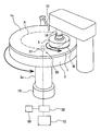
- FIG. 1 is a view showing a polishing apparatus according to an embodiment of the present invention
- FIG. 2 is a cross-sectional view showing a detailed structure of a polishing head
- FIG. 3 is a schematic cross-sectional view showing the polishing apparatus including an optical film-thickness measuring device
- FIG. 4 is a schematic diagram illustrative of the principle of the optical film-thickness measuring device
- FIG. 5 is a plan view showing a positional relationship between a wafer and a polishing table
- FIG. 6 is a diagram showing a spectrum produced by a processor
- FIG. 7 is a diagram illustrative of a process of determining a film thickness from a comparison between a measurement spectrum obtained and a plurality of reference spectra;
- FIG. 8 is a graph showing a relationship between a film thickness of a reference wafer and a polishing time
- FIG. 9 is a diagram showing a sampling spectrum and a reference spectrum
- FIG. 10 is a schematic diagram illustrative of a process of selecting one spectrum group from a plurality of spectrum groups
- FIG. 11 is a flowchart showing an example of a sequence of determining a film thickness at each revolution of the polishing table while one wafer is being polished;
- FIG. 12 is a diagram showing a configuration of a database system for managing the spectrum groups
- FIG. 13 is a diagram showing a film-thickness profile estimated using a plurality of spectrum groups while one target wafer is being polished;
- FIG. 14 is a diagram illustrative of a process of correcting a corresponding reference spectrum such that a polishing rate can be regarded as constant while a reference wafer is being polished;
- FIG. 15 is a diagram showing an effect of a corrected reference spectrum
- FIG. 16 is a graph showing a method of determining an estimation line shown in FIG. 14 ;
- FIG. 17 is a graph illustrative of another method of obtaining the estimation line.
- FIG. 18 is a diagram showing a film-thickness profile obtained by correcting a reference spectrum according to a method which uses an amount of change in spectrum, with respect to the target wafer and the spectrum groups shown in FIG. 13 ;
- FIG. 19 is a cross-sectional view showing a surface structure of a wafer
- FIG. 20 is a diagram showing a spectrum of reflected light that varies according to a depth of a recess formed in an underlying layer.
- FIG. 21 is a diagram showing a spectrum of reflected light that varies according to a width of a recess formed in an underlying layer.
- FIG. 1 is a view showing a polishing apparatus according to an embodiment of the present invention.
- the polishing apparatus includes a polishing table 3 to which a polishing pad 1 having a polishing surface 1 a is attached, a polishing head 5 for holding a wafer W, which is an example of a substrate, and polishing the wafer W while pressing it against the polishing pad 1 on the polishing table 3 , a polishing-liquid supply nozzle 10 for supplying a polishing liquid (e.g., a slurry) onto the polishing pad 1 , and a polishing controller 12 for controlling polishing of the wafer W.
- a polishing liquid e.g., a slurry
- the polishing table 3 is coupled to a table motor 19 through a table shaft 3 a .
- the table motor 19 is disposed below the polishing table 3 , and is configured to rotate the polishing table 3 in a direction indicated by arrow.
- the polishing pad 1 is attached to an upper surface of the polishing table 3 .
- the polishing pad 1 has an upper surface serving as a polishing surface 1 a for polishing the wafer W.
- the polishing head 5 is coupled to a lower end of a polishing head shaft 16 .
- the polishing head 5 is configured to be able to hold the wafer W on its lower surface by vacuum suction.
- the polishing head shaft 16 can be moved up and down by an elevating mechanism which is not shown.
- Polishing of the wafer W is performed as follows.
- the polishing head 5 and the polishing head 3 are rotated individually in directions indicated by arrows, and the polishing-liquid supply nozzle 10 supplies the polishing liquid (or slurry) onto the polishing pad 1 .
- the polishing head 5 presses the wafer W against the polishing surface 1 a of the polishing pad 1 .
- the surface of the wafer W is polished by a mechanical action of abrasive grains contained in the polishing liquid and a chemical action of the polishing liquid.
- FIG. 2 is a cross-sectional view showing a detailed structure of the polishing head 5 .
- the polishing head 5 includes a carrier 6 in the form of a circular plate, a circular flexible elastic membrane 7 which defines a plurality of pressure chambers D 1 , D 2 , D 3 , D 4 beneath the carrier 6 , and a retainer ring 8 for pressing the polishing pad 1 .
- the retainer ring 8 is disposed around the wafer W.
- the pressure chambers D 1 , D 2 , D 3 , D 4 are formed between the elastic membrane 7 and a lower surface of the carrier 6 .
- the elastic membrane 7 has a plurality of annular partition walls 7 a , which isolate the pressure chambers D 1 , D 2 , D 3 , D 4 from each other.
- the central pressure chamber D 1 is of a circular shape, and the other pressure chambers D 2 , D 3 , D 4 are annular in shape.
- the pressure chambers D 1 , D 2 , D 3 , D 4 are in concentric arrangement.
- the polishing head 5 may have only one pressure chamber, or may have five or more pressure chambers.
- the pressure chambers D 1 , D 2 , D 3 , D 4 are coupled to fluid lines G 1 , G 2 , G 3 , G 4 , respectively, so that pressurized fluid (e.g., pressurized gas, such as pressurized air) having regulated pressure(s) is supplied through the fluid lines G 1 , G 2 , G 3 , G 4 into the pressure chambers D 1 , D 2 , D 3 , D 4 .
- pressurized fluid e.g., pressurized gas, such as pressurized air
- Vacuum lines U 1 , U 2 , U 3 , U 4 are coupled to the fluid lines G 1 , G 2 , G 3 , G 4 , respectively, so that negative pressures can be created in the pressure chambers D 1 , D 2 , D 3 , D 4 by the vacuum lines U 1 , U 2 , U 3 , U 4 .
- the internal pressures in the pressure chambers D 1 , D 2 , D 3 , D 4 can be varied independently of each other for thereby independently regulating polishing pressures on corresponding four areas of the wafer W, i.e., a central area, an inner intermediate area, an outer intermediate area, and a peripheral area.
- An annular elastic membrane 9 is disposed between the retainer ring 8 and the carrier 6 .
- An annular pressure chamber D 5 is formed in this elastic membrane 9 .
- the pressure chamber D 5 is coupled to a fluid line G 5 , so that pressurized fluid (e.g., pressurized air) having regulated pressure can be supplied through the fluid line G 5 into the pressure chamber D 5 .
- a vacuum line U 5 is coupled to the fluid line G 5 so that a negative pressure can be created in the pressure chamber D 5 by the vacuum line U 5 .
- the entirety of the retainer ring 8 can move up and down.
- the pressure in the pressure chamber D 5 is applied to the retainer ring 8 , which is in turn able to directly press the polishing pad 1 independently of the elastic membrane 7 .
- the retainer ring 8 presses the polishing pad 1 around the wafer W, and the elastic membrane 7 presses the wafer W against the polishing pad 1 .
- the carrier 6 is fixed to a lower end of the head shaft 16 , which is coupled to an elevating mechanism 20 .
- This elevating mechanism 20 is configured to elevate and lower the head shaft 16 and the polishing head 5 , and to position the polishing head 5 at a predetermined height.
- the elevating mechanism 20 which functions as a polishing-head positioning mechanism, may comprise a combination of a servomotor and a ball screw mechanism.
- the pressure chambers D 1 through D 5 are supplied with the pressurized fluid.
- the elastic membrane 7 presses the wafer W against the polishing pad 1 .
- the retainer ring 8 presses the polishing pad 1 . The wafer W is polished in this state.
- the polishing apparatus includes an optical film-thickness measuring device 25 for obtaining a film thickness of the wafer W.
- This optical film-thickness measuring device 25 has a film thickness sensor 31 for obtaining an optical signal that varies in accordance with the film thickness of the wafer W, and a processor 32 for determining the film thickness from the optical signal.
- the film thickness sensor 31 is disposed in the polishing table 3 , and the processor 32 is coupled to the polishing controller 12 .
- the film thickness sensor 31 rotates together with the polishing table 3 as indicated by arrow A, and obtains the optical signal of the wafer W held on the polishing head 5 .
- the film thickness sensor 31 is coupled to the processor 32 so that the optical signal, obtained by the film thickness sensor 31 , is sent to the processor 32 .
- FIG. 3 is a schematic cross-sectional view showing the polishing apparatus having the optical film-thickness measuring device 25 .
- the polishing head shaft 16 is coupled to a polishing head motor 18 through a coupling device 17 , such as belt, so that the polishing head shaft 16 is rotated by the polishing head motor 18 .
- This rotation of the polishing head shaft 16 is transmitted to the polishing head 5 to rotate the polishing head 5 in the direction indicated by the arrow.
- the optical film-thickness measuring device 25 includes the film thickness sensor 31 and the processor 32 .
- the film thickness sensor 31 is configured to emit light to the surface of the wafer W, receive the light reflected from the wafer W, and break up the reflected light according to wavelength.
- the film thickness sensor 31 includes an light emitter 42 for irradiating the surface, to be polished, of the wafer W with the light, an optical fiber 43 as a light receiver for receiving the reflected light from the wafer W, a spectrometer 44 configured to resolve the reflected light according to wavelength and measure intensity of the reflected light over a predetermined wavelength range.
- the polishing table 3 has a first hole 50 A and a second hole 50 B having upper open ends lying in the upper surface of the polishing table 3 .
- the polishing pad 10 has a through-hole 51 at a position corresponding to the holes 50 A and 50 B.
- the holes 50 A and 50 B are in fluid communication with the through-hole 51 , which has an upper open end lying in the polishing surface 1 a .
- the first hole 50 A is coupled to a liquid supply source 55 via a liquid supply passage 53 and a rotary joint (not shown).
- the second hole 50 B is coupled to a liquid discharge passage 54 .
- the light emitter 42 includes a light source 47 for emitting multiwavelength light and an optical fiber 48 coupled to the light source 47 .
- the optical fiber 48 is an optical transmission element for transmitting the light, emitted by the light source 47 , to the surface of the wafer W.
- the distal ends of the optical fiber 48 and the optical fiber 43 lie in the first hole 50 A and are located near the surface, to be polished, of the wafer W.
- the distal ends of the optical fiber 48 and the optical fiber 43 are arranged so as to face the wafer W held by the polishing head 5 , so that multiple areas of the wafer W are irradiated with the light each time the polishing table 3 makes one revolution.
- the distal ends of the optical fiber 48 and the optical fiber 43 are located so as to pass across the center of the wafer W held by the polishing head 5 .
- the liquid supply source 55 supplies water (preferably pure water) as a transparent liquid into the first hole 50 A through the liquid supply passage 53 .
- the water fills a space formed between the lower surface of the wafer W and the distal ends of the optical fibers 48 , 43 .
- the water further flows into the second hole 50 B and is expelled therefrom through the liquid discharge passage 54 .
- the polishing liquid is discharged together with the water and thus a path of light is ensured.
- the liquid supply passage 53 is provided with a valve (not shown in the drawing) configured to operate in conjunction with the rotation of the polishing table 3 . The valve operates so as to stop the flow of the water or reduce the flow of the water when the wafer W is not located over the through-hole 51 .
- the optical fiber 48 and the optical fiber 43 are arranged in parallel with each other.
- the distal ends of the optical fiber 48 and the optical fiber 43 are perpendicular to the surface of the wafer W, so that the optical fiber 48 casts the light onto the surface of the wafer W perpendicularly.
- the light emitter 42 directs the light to the wafer W, and the optical fiber (or the light receiver) 43 receives the light reflected from the wafer W.
- the spectrometer 44 measures the intensity of the reflected light at each of the wavelengths over the predetermined wavelength range and sends light intensity data to the processor 32 .
- the light intensity data is the optical signal reflecting the film thickness of the wafer W, and contains intensities of the reflected light and corresponding wavelengths.
- the processor 32 produces a spectrum showing the light intensities at the respective wavelengths from the light intensity data, and further determines the film thickness of the wafer W from the spectrum.
- FIG. 4 is a schematic view illustrating the principle of the optical film-thickness measuring device 25
- FIG. 5 is a plan view showing a positional relationship between the wafer W and the polishing table 3 .
- the wafer W has a lower film and an upper film formed on the lower film.
- the upper film is, for example, a silicon layer or a dielectric film.
- the light emitter 42 and the light receiver 43 are oriented toward the surface of the wafer W.
- the light emitter 42 is configured to direct the light to multiple areas, including the center, of the wafer W each time the polishing table 3 makes one revolution.
- the light which is cast on the wafer W, is reflected off an interface between a medium (e.g., water in the example of FIG. 4 ) and the upper film and an interface between the upper film and the lower film.
- a medium e.g., water in the example of FIG. 4
- Light waves from these interfaces interfere with each other.
- the manner of interference between the light waves varies according to the thickness of the upper film (i.e., a length of an optical path).
- the spectrum produced from the reflected light from the wafer, varies according to the thickness of the upper film.
- the spectrometer 44 breaks up the reflected light according to the wavelength and measures the intensity of the reflected light at each of the wavelengths.
- the processor 32 produces the spectrum from the intensity data of the reflected light (i.e., the optical signal) obtained from the spectrometer 44 .
- a spectrum produced from the reflected light from the wafer W to be polished will be referred to as measurement spectrum.
- This measurement spectrum is expressed as a line graph (i.e., a spectral waveform) indicating a relationship between the wavelength and the intensity of the light.
- the intensity of the light can also be expressed as a relative value, such as a reflectance or a relative reflectance.
- FIG. 6 is a diagram showing a measurement spectrum created by the processor 32 .
- horizontal axis represents the wavelength of the light reflected from the wafer
- vertical axis represents relative reflectance derived from the intensity of the reflected light.
- the relative reflectance is an index that represents reflection intensity of light. More specifically, the relative reflectance is a ratio of the intensity of the light to a predetermined reference intensity.
- unwanted noises such as a variation in the intensity inherent in an optical system or the light source, are removed from the actually measured intensity.
- a measurement spectrum reflecting only the film thickness information can be obtained.
- the reference intensity is an intensity obtained in advance at each of the wavelengths.
- the relative reflectance is calculated at each of the wavelengths. More specifically, the relative reflectance is determined by dividing the intensity of the light (i.e., the actually measured intensity) at each of the wavelengths by a corresponding reference intensity.
- the reference intensity may be an intensity of light from a silicon wafer (bare wafer) with no film thereon which is being water-polished in the presence of water.
- the relative reflectance is obtained as follows. A dark level (which is a background intensity obtained under the condition that light is cut off) is subtracted from the actually measured intensity to determine a corrected actually measured intensity. Further, the dark level is subtracted from the reference intensity to determine a corrected reference intensity. Then the relative reflectance is calculated by dividing the corrected actually measured intensity by the corrected reference intensity.
- a relative reflectance R( ⁇ ) can be calculated by using the following equation (1).
- the processor 32 is configured to determine the film thickness from a comparison between the measurement spectrum and a plurality of reference spectra.
- the optical film-thickness measuring device 25 is coupled to a storage device 58 show in FIG. 1 and FIG. 3 .
- the plurality of reference spectra are stored in this storage device 58 .
- FIG. 7 is a diagram illustrating a process of determining the film thickness from the comparison between the measurement spectrum and the plurality of reference spectra.
- the processor 32 compares the spectrum, which is produced when the wafer is being polished, with the plurality of reference spectra so as to determine a reference spectrum which is closest in shape to the measurement spectrum, and obtains a film thickness which has been associated with the determined reference spectrum.
- the reference spectrum which is closest in shape to the measurement spectrum is a spectrum with the smallest difference in the relative reflectance between the reference spectrum and the measurement spectrum.
- the plurality of reference spectra are those obtained in advance by polishing a reference wafer having an initial film thickness which is the same as or equivalent to that of the wafer which is an object of polishing (which may be hereinafter referred to as target wafer or target substrate).
- Each reference spectrum can be associated with a film thickness at a point in time when that reference spectrum is obtained. Specifically, each reference spectrum is obtained at a different film thickness, and the plurality of reference spectra correspond to different film thicknesses. Therefore, the current film thickness can be estimated by identifying a reference spectrum whose shape is most similar to the shape of the measurement spectrum.
- a reference wafer having a film thickness which is the same as or equivalent to that of a target wafer, is prepared.
- the reference wafer is transported to a not-shown film-thickness measuring unit, which then measures an initial film thickness of the reference wafer.
- the reference wafer is transported to the polishing apparatus shown in FIG. 1 , where the reference wafer is polished while the slurry as the polishing liquid is supplied onto the polishing pad 1 .
- the light is directed to the surface of the reference wafer, and a spectrum (i.e., a reference spectrum) of reflected light from the reference wafer is obtained.
- the reference spectrum is obtained each time the polishing table 3 makes one revolution. Therefore, a plurality of reference spectra are obtained during the polishing process of the reference wafer.
- the reference wafer is transported again to the aforementioned film-thickness measuring unit, which then measures a film thickness (i.e., a final film thickness) of the polished reference wafer.
- FIG. 8 is a graph showing a relationship between film thickness of the reference wafer and polishing time. If a polishing rate of the reference wafer is constant, as shown in FIG. 8 , the film thickness linearly decreases with the polishing time. In other words, the film thickness can be expressed with use of a linear function which includes the polishing time as a variable. The polishing rate can be calculated by dividing a difference between the initial film thickness Tini and the final film thickness Tfin by the polishing time t at which the final film thickness Tfin is reached.
- a polishing time at which each reference spectrum was obtained can be calculated from a rotational speed of the polishing table 3 .
- Each reference spectrum can be associated (or connected) with a corresponding film thickness. Therefore, the processor 32 can identify a reference spectrum which is closest in shape to the measurement spectrum while a wafer is being polished, and can determine the current film thickness from a film thickness that has been associated with the identified reference spectrum.
- a cross-sectional structure of a wafer, to be polished (i.e., a target wafer)
- a cross-sectional structure of a wafer, to be polished (i.e., a target wafer)
- a cross-sectional structure of a wafer, to be polished i.e., a target wafer
- This simulation is conducted by building or creating a structure of a target wafer in a computer and simulating a spectrum which is obtained when the target wafer is irradiated with light, while reducing the film thickness of the wafer gradually. In this manner, it is possible to obtain a plurality of reference spectra corresponding to different film thicknesses from the simulation on the computer.
- the spectrum of the reflected light varies in accordance with the film thickness. Consequently, if the film thickness remains unchanged, the spectrum also remains unchanged. However, as shown in FIG. 20 and FIG. 21 , even if the film thickness is the same, the spectrum may change due to a difference in structure of an underlying layer existing beneath the film.
- the structure of the underlying layer may vary from area to area in the surface of the wafer, or may vary from wafer to wafer. Such a difference in the structure of the underlying layer prevents accurate measuring of the film thickness.
- the processor 32 is configured to determine a film thickness using a plurality of spectrum groups each containing a plurality of reference spectra corresponding respectively to different film thicknesses.
- the processor 32 is coupled to the storage device 58 which stores the plurality of spectrum groups therein.
- the reference spectra contained in these different spectrum groups are either reference spectra produced from light reflected from different areas of the reference wafer, or reference spectra obtained using a plurality of reference wafers, or reference spectra obtained from a simulation of light reflection.
- one reference wafer having a film thickness which is the same as or equivalent to that of a target wafer, is used.
- the film thickness of the reference wafer may be larger than the film thickness of the target wafer.
- the film thickness of the reference wafer may be slightly smaller than the film thickness of the target wafer.
- a plurality of reference spectra are produced from the light reflected from these areas, and the reference spectra produced are classified according to the areas, whereby a plurality of spectrum groups are obtained.
- the structure of the underlying layer varies slightly from area to area of the reference wafer. Therefore, a plurality of spectrum groups which reflect the difference in the structure of the underlying layer are obtained.
- a plurality of reference wafers each having a film thickness, which is the same as or equivalent to that of a target wafer, are used.
- the film thicknesses of the reference wafers may be larger than the film thickness of the target wafer. Given that the film thickness cannot accurately be determined during an initial polishing stage, the film thicknesses of the reference wafers may be slightly smaller than the film thickness of the target wafer.
- One reference wafer is selected from the plurality of reference wafers.
- the reference wafer While the selected reference wafer is being polished, the reference wafer is irradiated with the light, and a plurality of reference spectra are produced from the light reflected from the reference wafer, so that one or more spectrum groups are obtained.
- the process of irradiating the selected reference wafer with the light and the process of obtaining one or more spectrum groups are repeated, while changing the reference substrate, to be selected, from one to another each time the process of irradiating the reference wafer and the process of obtaining one or more spectrum groups are repeated, until all the reference wafers are polished, so that a plurality of spectrum groups are obtained.
- the structure of the underlying layer varies slightly between the reference wafers. Therefore, a plurality of spectrum groups which reflect the difference in the structure of the underlying layer are obtained. If the structure of the underlying layer is different not only between wafers but also between areas in a wafer surface, spectrum groups are obtained in a plurality of areas of each of the reference wafers.
- the processor 32 produces a spectrum from the reflected light from the target wafer, and selects a spectrum group containing a reference spectrum which is closest in shape to the produced spectrum.
- This spectrum used to select a spectrum group will hereinafter be referred to as sampling spectrum.
- the sampling spectrum is a spectrum produced from the light reflected from the wafer W to be polished.
- the comparison in shape between the sampling spectrum and the reference spectrum is performed on the basis of a deviation of the reference spectrum from the sampling spectrum. More specifically, the processor 32 calculates the deviation between these two spectra with use of the following equation.
- ⁇ U ⁇ ⁇ ⁇ ⁇ 1 ⁇ ⁇ ⁇ 2 ⁇ ⁇ Rc ⁇ ( ⁇ ) - Rp ⁇ ( ⁇ ) ⁇ ( 2 )
- ⁇ represents a wavelength of light
- ⁇ 1 , ⁇ 2 represent upper limit and lower limit that determine a wavelength range of the spectrum to be monitored
- Rc represents a relative reflectance that constitutes the sampling spectrum
- Rp represents a relative reflectance that constitutes the reference spectrum.
- preprocessing may be carried out on Rc and Rp.
- Examples of such preprocessing may include a normalizing process wherein each of Rc and Rp is divided by an average wavelength, an averaging process wherein values of Rc and Rp and those in an adjacent measuring area are averaged, and a time-averaging process wherein the measured value of Rc and Rp and those in several steps in the past are averaged.
- FIG. 9 is a diagram showing the sampling spectrum and the reference spectrum.
- the above equation (2) is an equation for calculating the deviation of the reference spectrum from the sampling spectrum. This deviation corresponds to a region (a hatched region shown in FIG. 9 ) enclosed by these two spectra.
- the processor 32 determines a reference spectrum with the smallest deviation from the sampling spectrum, i.e., a reference spectrum which is closest in shape to the sampling spectrum. The processor 32 then selects, from the plural spectrum groups, a spectrum group to which the determined reference spectrum belongs.
- FIG. 10 is a schematic diagram illustrative of a process of selecting one spectrum group from the plurality of spectrum groups.
- the storage device 58 (see FIGS. 1 and 3 ) stores the plurality of spectrum groups as shown in FIG. 10 in advance.
- Each of the spectrum groups contains a plurality of reference spectra corresponding respectively to different film thicknesses of a film to be polished.
- the processor 32 produces a sampling spectrum from the light reflected from the target wafer and determines (or selects) a spectrum group containing a reference spectrum which is closest in shape to the sampling spectrum produced.
- the plurality of spectrum groups are obtained under a condition that the structure of the underlying layer is different. Therefore, the reference spectra are different between the spectrum groups due to the difference in the structure of the underlying layer. The influence of the difference in the structure of the underlying layer can be eliminated by selecting a spectrum group containing the reference spectrum which is closest in shape to the sampling spectrum. As a result, the processor 32 can obtain a more accurate film thickness.
- the areas (hereinafter referred to as “reference areas”) defined on a wafer surface where the spectrum groups are obtained may be a plurality of reference areas defined by a plurality of radius ranges.
- reference areas defined by a plurality of radius ranges.
- the thickness of the underlying layer varies generally in approximately an axisymmetric manner within the wafer surface because of the characteristics of a film deposition process prior to the polishing process and the polishing process itself
- the rotational speeds of the polishing table 3 and the polishing head 5 are set so as to cause the film thickness sensor 31 to scan the wafer surface uniformly in a circumferential direction of the wafer surface and return to its original position within a predetermined short time, the influence of variation in the structure of the underlying layer in the circumferential direction of the wafer can be reduced by averaging spectral data obtained in the predetermined short time.
- the polishing head 5 makes eleven revolutions until the film thickness sensor 31 returns to its original position on the wafer surface, while the polishing table 3 makes ten revolutions. Therefore, the influence of variation in the structure of the underlying layer in the wafer surface can greatly be reduced by averaging spectral data obtained during the ten revolutions of the polishing table 10 .
- the structure of the underlying layer of the reference wafer can be measured before or after the reference wafer is polished with use of a standalone film-thickness measuring unit or an inline film-thickness measuring unit which is assembled in the polishing apparatus.
- a thickness or a structure of the underlying layer is measured while the reference wafer is in a stationary state. It is preferable that, based on a distribution of measured thicknesses of the underlying layer of one or more reference wafers, reference areas be selected in each of the reference wafers so that the thicknesses of the underlying layer are distributed as uniformly as possible over an entirety of a range from the smallest thickness to the largest thickness. A plurality of spectrum groups are obtained in each of the selected reference areas.
- reference areas may preferably be determined so as to be distributed as uniformly as possible over the surface of each reference wafer. Furthermore, it is more preferable to narrow down the number of spectrum groups in advance by eliminating a spectrum group containing reference spectra which are close in shape to those of another spectrum group. The similarity in shape between the reference spectra can be determined using the above-described equation (2).
- the reference spectrum may have maximum local points and minimum local points which can vary depending on the structure of the underlying layer.
- attention may be directed to wavelengths of the maximum local points or the minimum local points, and a reference area of the reference wafer may be selected such that all of the wavelengths of the maximum local points or the minimum local points are distributed as uniformly as possible within a range from the smallest wavelength to the largest wavelength.
- the process of selecting the spectrum group may be carried out while the target wafer is being polished or before the target wafer is polished. If the spectrum group is selected while the target wafer is being polished, it is preferable to use a sampling spectrum which has been produced within a preset polishing time. For example, a sampling spectrum to be used may be produced until a predetermined time elapses from the start of the polishing. This sampling spectrum is compared with a plurality of reference spectra in the plurality of spectrum groups, and a spectrum group containing a reference spectrum, which is closest in shape to the sampling spectrum, is selected.
- a spectrum group is selected before the target wafer is polished, it is preferable to use a sampling spectrum produced while the target wafer is being water-polished.
- This water-polishing process is a process in which the target wafer is placed in sliding contact with the polishing pad while pure water, rather than the slurry, is being supplied onto the polishing pad.
- the target wafer is water-polished in the presence of the pure water existing between the target wafer and the polishing pad. Unlike the slurry, the pure water does not contain abrasive grains and does not have an etching action on a film of the wafer. Accordingly, polishing of the target wafer does not substantially progress when the target water is being water-polished.
- spectrum groups have been determined using the standalone film-thickness measuring unit or the inline film-thickness measuring unit, it is possible to measure the structure and/or the thickness of the underlying layer of the target wafer with use of the inline film-thickness measuring unit assembled in the polishing apparatus and to select a corresponding spectrum group.
- each time one target wafer is polished it is preferable to measure the underlying layer of that target wafer. If structures of underlying layers in one lot are regarded as being uniform, one target wafer in each lot may be measured.
- measuring of the thickness may be performed on two target wafers, one of which is selected from the odd-numbered group and other is selected from the even-numbered group.
- the processor 32 produces the measurement spectrum during polishing of the target wafer, and selects a reference spectrum, which is closest in shape to the produced measurement spectrum, from the spectrum group that has been selected as discussed above. More specifically, the processor 32 uses the equation (2) to determine a reference spectrum that is closest in shape to the measurement spectrum, i.e., a reference spectrum with the smallest deviation from the measurement spectrum, and obtains a film thickness that has been associated with the determined reference spectrum. The processor 32 monitors the polishing process of the target wafer based on the determined film thickness, and determines a polishing endpoint at which the film thickness is lower than a predetermined target value.
- the processor 32 sends a polishing endpoint detection signal to the polishing controller 12 , which in turn terminates polishing of the target wafer in response to the polishing endpoint detection signal.
- the processor 32 determines manipulated variables (or control variables) for obtaining a predetermined distribution of remaining film thicknesses, on the basis of the film thicknesses determined in the respective areas on the surface of the target wafer.
- the manipulated variables (or control variables) may be pressure command values for the pressure chambers D 1 through D 5 .
- the processor 32 sends these pressure command values to the polishing controller 12 , which updates the pressures based on the command values that have been sent to the polishing controller 12 .
- the measurement spectrum may vary greatly due to some factors, such as a temperature of the target wafer, a change in the shape of the surface of the target wafer, etc.
- asperities or steps
- the measurement spectrum may vary greatly.
- the measurement spectrum is relatively unstable depending on the state of the asperities, and may vary between wafers or between areas within the surface of the wafer.
- a stable measurement spectrum is likely to be obtained.
- the processor 32 may produce a sampling spectrum again during the polishing process of the target wafer, and may select again a spectrum group containing a reference spectrum which is closest in shape to this sampling spectrum produced. Since the sampling spectrum produced during the polishing process of the target wafer is substantially the same as the measurement spectrum, the measurement spectrum may be used as the sampling spectrum. After the spectrum group has been selected again, the processor 32 selects a reference spectrum, which is closest in shape to the measurement spectrum, from the spectrum group that has been selected again. By thus selecting the spectrum group again, a more accurate film thickness can be obtained especially in a latter half of the polishing process which has an important significance for a finishing performance.
- a plurality of spectrum groups obtained in areas near the area where the film thickness of the target wafer is to be monitored may be selected in advance.
- a plurality of spectrum groups obtained in a peripheral portion of a reference wafer may preferably be selected in advance from all the spectrum groups, and a spectrum group containing a reference spectrum, which is closest in shape to the sampling spectrum, may preferably be selected from these spectrum groups that have been selected in advance.
- the structure of the underlying layer may often vary from area to area within the surface of the wafer.
- the film thickness sensor 31 may often scan the same position on the wafer surface in the same direction in the same area of the wafer surface. Simultaneous using of the above-described setting of the rotational speeds of the polishing table 3 and the polishing head 5 and the above-described averaging calculation of spectral data can reduce the influence of interconnect patterns in the measurement areas. Consequently, an accurate film thickness can be measured efficiently by selecting, in advance, several spectrum groups obtained in areas near the area to be monitored.
- the reference spectra are obtained in advance using the reference wafer(s) or by the simulation.
- the reference spectra thus obtained may include reference spectra which are similar in shape between spectrum groups.
- the processor 32 is able to compare the sampling spectrum with the reference spectra in a shorter time.
- FIG. 11 shows an example of a flow of determining a film thickness in each revolution of the polishing table 3 while one wafer is being polished, with an attention directed to the selection of spectrum.
- Determining a film thickness of a target wafer based on a comparison between a measurement spectrum (and a sampling spectrum) and reference spectra may hereinafter be referred to as estimating a film thickness. This is because, according to the present embodiment, a film thickness of a target wafer is determined by way of the calculation based on information about an actually measured value of an initial film thickness of a reference wafer, an actually measured value of a final film thickness of the reference wafer, and a polishing time of the reference wafer.
- step 1 at each of measurement points on a target wafer, a sampling spectrum of the reflected light is obtained while the polishing table 3 is making one revolution.
- step 2 the processor 32 determines whether the polishing table 3 has made a predetermined number of revolutions NM after polishing of the target wafer is started.
- a subsequent flow of film thickness estimation is different depending on a magnitude relationship between the present number of revolutions of the polishing table 3 and the predetermined number of revolutions NM.
- initial film thickness i.e., film thickness prior to polishing
- the predetermined number of revolutions NM is set such that the film thickness of the target wafer can sufficiently be lower than the initial film thickness of the reference wafer as a result of polishing of the target wafer, even if the target wafer has the initial film thickness which corresponds to the largest value in the range of the variation. This is because the film thickness estimation based on the comparison with the reference spectra can determine a film thickness of the target wafer only within a range of film thicknesses corresponding to those of the reference spectra.
- the number of revolutions NM is set to be a suitable number in view of the fact that a thickness and an optical constant of the underlying layer in each area of the wafer surface do not vary during the polishing process. If a sampling spectrum cannot be determined during a certain number of revolutions at an initial stage of the polishing process for a certain reason, e.g., for a reason of a moving average of spectra, that number of revolutions may be added to NM.
- the processor 32 calculates deviations of the reference spectra, which belong to all the spectrum groups (all reference area candidates), from the sampling spectrum (step 3 ).
- the reference spectra which are subject to the calculation of the deviations in this step 3 are reference spectra of all the spectrum groups that have been obtained during a period from when the polishing of the reference wafer is started until a predetermined number of table revolutions NR is reached.
- the predetermined number of table revolutions NR is set such that some of film thickness candidates corresponding to the reference spectra can sufficiently be lower than the initial film thickness of the target wafer even if the target wafer has an initial film thickness which is equal to the smallest value of the range of the variation in the initial film thickness of the target wafer. Furthermore, it is preferable that the number of table revolutions NR be set to be a suitable numerical value in view of the calculation load and a change in the film thickness of the target wafer during the number of revolutions NM.
- step 4 the processor 32 selects the smallest one of the deviations determined in the step 3 (i.e., the smallest deviation) with respect to each of the measurement points on the target wafer, selects a spectrum group to which a reference spectrum, corresponding to the selected smallest deviation, belongs, and estimates the film thickness of the target wafer from the film thicknesses measured before and after the processing process and the polishing time of the selected spectrum group, and from the polishing time (i.e., the time that has elapsed from the polishing start) of the reference spectrum with the smallest deviation.
- the processor 32 stores the selected spectrum group (reference area candidate).
- the processor 32 may also store the smallest deviation.
- steps 5 , 6 if the present number of revolutions of the polishing table 3 is equal to the predetermined number of revolutions NM, one optimum spectrum group (or an optimum reference area) is determined at each of the measurement points on the target wafer on the basis of the selection results in the step 4 that have been obtained during table revolutions in the past.
- an optimum spectrum group may be determined as follows:
- a spectrum group (or a reference area candidate) with the highest frequency of the smallest deviation determined in the step 4 is determined to be an optimum spectrum group (or an optimum reference area);
- a spectrum group (or a reference area candidate) with the smallest one of the smallest deviations determined in the step 4 is determined to be an optimum spectrum group (or an optimum reference area).
- the measurement spectrum obtained in each of the measurement points on the target wafer is compared with the reference spectra which belong to the optimum spectrum group determined in the step 6 , and spectrum deviations are calculated (step 7 ).
- a range of the revolutions in which the reference spectra are to be compared is not the revolutions NR in the initial stage of the polishing process, but should be determined in view of the change in the film thickness which occurs as polishing of the wafer progresses, and may be a total revolution range (i.e., a total film-thickness range).
- step 8 the processor 32 determines a polishing time (i.e., a time that has elapsed from the polishing start) allocated to a reference spectrum with the smallest spectrum deviation calculated in step 7 at each of the measurement points on the target wafer, and calculates a film thickness.
- step 9 the processor 32 determines whether the polishing process is to be terminated on the basis of a designated polishing time or a polishing endpoint detection or other criterion. If the polishing process is not to be terminated, then the step 1 is carried out again. If sufficient calculation resources are available, the numbers of revolutions NM, NR may be set to be sufficiently large values in the steps 2 , 3 . In this case, the steps 1 through 5 and the step 9 are repeated throughout the polishing process.
- FIG. 12 is a diagram showing a configuration of a database system for managing the above-described spectrum groups.
- a data server 60 has a spectrum group database 61 constructed therein.
- the spectrum group database 61 stores therein identification information of spectrum groups, reference spectra belonging to each one of the spectrum groups, and associated film thickness information.
- the data server 60 is coupled to one or more polishing apparatuses 70 via a network, so that the one or more polishing apparatuses 70 can share the spectrum group database 61 .
- reference spectra and information of film thickness before and after the polishing process, which have been obtained in each polishing apparatus 70 are sent to the data server 60 , where they are registered in the spectrum group database 61 .
- the polishing apparatuses 70 which polish wafers of the same specification (i.e., the same product, the same layers), may preferably share the single spectrum group database 61 .
- each polishing apparatus 70 When each polishing apparatus 70 is about to polish a target wafer and determine a film thickness, predetermined spectrum groups are automatically downloaded from the spectrum group database 61 , as indicated by solid lines shown in FIG. 12 .
- the spectrum groups to be downloaded may be designated as a part of a polishing recipe. Thereafter, each polishing apparatus 70 selects a spectrum group and calculates a film thickness at each of the measurement points, as described above. In addition, the polishing apparatus 70 saves information about the actually selected spectrum group into a storage area thereof.
- the information about the selected spectrum group is automatically sent to the data server 60 , where the information is registered as history information in a spectrum group selection history database 62 .
- the spectrum group selection history database 62 and the spectrum group database 61 are organically linked to each other through spectrum group identification numbers serving as a common key.
- the spectrum group selection history database 62 may be constructed integrally with the spectrum group database 61 .
- the data server 60 deletes a spectrum group, which has not actually been selected or have been selected very few times within a predetermined period of time, from the database 61 on the basis of the history information about the selection of spectrum groups.
- the data server 60 also ranks spectrum groups and adjusts the ease with which to select them, on the basis of frequency of the selection.
- FIG. 13 is a diagram showing a film-thickness profile estimated using a plurality of spectrum groups while one target wafer is being polished.
- the film-thickness profile shown in FIG. 13 was plotted about every 10 seconds.
- spectrum groups i.e., reference wafers and reference areas
- the spectrum group for use in estimating a film thickness is switched at a radial position of about 50 mm between a spectrum group A (obtained in a central area of a reference wafer) and a spectrum group B (obtained in an area at a radial position of about 100 mm on a reference wafer).
- steps are generated in the film-thickness profile.
- Such steps are due to an assumption that a polishing rate of a reference wafer used to construct each spectrum group is constant during polishing and the film thickness decreases linearly.
- a polishing rate is not strictly constant in each area in the wafer surface, and the manner of change in the polishing rate is different between areas.
- steps appear in the film-thickness profile at the radial position of about 50 mm due to the switching of the spectrum groups.
- Such steps in the film-thickness profile may lower the controlling performance, particularly when a distribution of remaining film thickness (i.e., a profile) is controlled.
- FIG. 14 is a diagram illustrative of a process of correcting a reference spectrum.
- dot-and-dash line in FIG. 14 represents a hypothetical line indicating a change in the film thickness with time on the assumption that the polishing rate is constant during polishing of the reference wafer.
- the film thickness on the assumption that the polishing rate is constant varies linearly with the polishing time from an initial film thickness (i.e., a film thickness measured before the polishing process) denoted by a symbol ⁇ to a final film thickness (i.e., a film thickness measured after the polishing process).
- the initial film thickness and the final film thickness are measured by the standalone film-thickness measuring unit or the inline film-thickness measuring unit.
- a curved line depicted by a solid line represents an estimation line indicating a change in the film thickness of the reference wafer with time, and reflects a change in the polishing rate. This estimation line passes through the initial film thickness and the final film thickness denoted by the symbol ⁇ .
- the determined corrected reference spectra can be regarded as reference spectra in the case where the polishing rate of the reference area of the corresponding reference wafer is constant throughout the polishing time.
- ⁇ 1 represents a film thickness of the target wafer at a certain point in time. If the reference spectra are not corrected, a spectrum corresponding to the film thickness ⁇ 1 corresponds to (i.e., is equal or close to) a reference spectrum at the point B on the estimation line. Generally, since it is assumed that the film thickness varies linearly, i.e., the polishing rate is constant, during polishing of the reference wafer, the calculated film thickness of the target wafer is ⁇ 2 , which is different from the actual film thickness ⁇ 1 .
- FIG. 16 is a graph showing a method of determining the above-described estimation line.
- a horizontal axis of the graph represents polishing time, and a vertical axis represents film thickness.
- a plurality of wafers (wafers W 1 to W 3 ) having the same specification and a reference wafer W 4 are polished for different set times. Film thicknesses of these wafers are measured before and after the polishing process by the standalone or inline film-thickness measuring unit. If initial film thicknesses (i.e., film thicknesses measured before the polishing process) of the wafers W 1 to W 3 are equal to an initial film thickness of the reference wafer W 4 , the initial film thickness is indicated by the symbol ⁇ on the vertical axis.
- Final film thicknesses i.e., film thicknesses measured after the polishing process, denoted by symbol ⁇ in FIG. 16
- the final film thickness denoted by the symbol ⁇
- the above estimation line is obtained by interpolating film thicknesses between the initial film thickness of the reference wafer W 4 , the final film thicknesses of the wafers W 1 to W 3 , and the final film thickness of the reference wafer W 4 .
- the initial film thickness of the wafers W 1 to W 3 is different from the initial film thickness of the reference wafer W 4 , a deviation from the initial film thickness of the reference wafer W 4 may be added to the final film thicknesses of the wafers W 1 to W 3 , so that the same operation can be achieved.
- FIG. 17 is a graph illustrative of another method of obtaining the estimation line.
- the spectrum of the reflected light from each of areas of the reference wafer varies during polishing of the reference wafer as the film thickness decreases.
- a value obtained by integrating a change ⁇ S in the relative reflectance per short time ⁇ t is approximately in agreement with an amount of polishing, i.e., a decrease in the film thickness.
- FIG. 18 is a diagram showing a result of a process of estimating a film-thickness profile with respect to the target wafer and the spectrum groups shown in FIG. 13 by correcting reference spectra according to the method using the above-described change in the spectrum. As can be seen from FIG. 18 , the steps at the boundary of the spectrum groups shown in FIG. 13 are eliminated, and a reliable film-thickness profile is obtained.
- the steps in the film-thickness profile as described above are not produced, and a film-thickness profile obtained is relatively correct. If the film thickness of the polished reference wafer is substantially the same as the film thickness of the polished target wafer, an absolute value of the film thickness for determining a polishing endpoint is considered to be correct as well. Even in such cases, however, the accuracy of the film-thickness estimation can be increased by correcting the reference spectra such that the polishing rate can be regarded as constant.
- the above-described steps that appear in the estimated film-thickness profile can be improved by using a change in wavelength at an extremum point (a peak or a valley) of the measurement spectrum obtained during the polishing process.
- a wavelength at the extremum point does not vary linearly with a decrease in a film thickness of a film being polished, and it is therefore difficult to express the change in the polishing rate with use of a quantitative value.
- the influence on the film-thickness estimation can be reduced by selecting one spectrum group of a certain reference wafer as a criterion and carrying out the operations described with reference to FIG. 14 using a curved line, drawn by the wavelength at the extremum point during the polishing process, as a hypothetical line.
- the spectrum of the reflected light varies not only with the film thickness of the film being polished, but also with the structure of the underlying layer.
- the spectrum of the reflected light varies even if the film thickness is the same.
- the film contains metal interconnects, the spectrum changes depending on the interconnect pattern and the interconnect density.
- an accurate film thickness can be determined by preparing a plurality of spectrum groups corresponding to different interconnect patterns and different interconnect densities, comparing them with each sampling spectrum of the target wafer, and selecting an optimum spectrum group.
- a measurement area in one measuring operation can be small.
- use of such light source can make it possible to increase the frequency with which interconnect patterns and interconnect densities contained in respective measurement areas are uniformized, thus making it easy to determine a more accurate film thickness.
- the present invention is applicable to a polishing method and a polishing apparatus for polishing a substrate, such as a wafer or the like, while measuring a film thickness thereof on the basis of optical information contained in reflected light from the substrate.
Abstract
Description
where λ is wavelength, E(λ) is the intensity of the light at the wavelength λ reflected from the wafer, B(λ) is the reference intensity at the wavelength λ, and D(λ) is the background intensity (i.e., the dark level) at the wavelength λ obtained under the condition that light is cut off.
where λ represents a wavelength of light, λ1, λ2 represent upper limit and lower limit that determine a wavelength range of the spectrum to be monitored, Rc represents a relative reflectance that constitutes the sampling spectrum, and Rp represents a relative reflectance that constitutes the reference spectrum. In view of the influences of variations in the intensity of the reflected light and noise due to the in-situ measuring process of the film thickness during polishing of the wafer, preprocessing may be carried out on Rc and Rp. Examples of such preprocessing may include a normalizing process wherein each of Rc and Rp is divided by an average wavelength, an averaging process wherein values of Rc and Rp and those in an adjacent measuring area are averaged, and a time-averaging process wherein the measured value of Rc and Rp and those in several steps in the past are averaged.
where Rp(λ,t) represents a relative reflectance at a wavelength λ and a time t, which may be preprocessed in the same manner as with the equation (2), S(t) represents a relative change in the spectrum at the time t where the change in the spectrum with respect to a total polishing time T is 1, and θpost and θpre represent film thicknesses which are measured by the standalone or inline film-thickness measuring unit before and after the polishing process, i.e., an initial film thickness and a final film thickness. θ(t) corresponds to the estimation line described above.
- 1 polishing pad
- 1 a polishing surface
- 3 polishing table
- 3 a table shaft
- 5 polishing head
- 6 carrier
- 7 elastic membrane
- 7 a partition wall
- 8 retainer ring
- 9 elastic membrane
- 10 polishing-liquid supply nozzle
- 12 polishing controller
- 16 polishing head shaft
- 17 coupling device
- 18 polishing head motor
- 19 table motor
- 20 elevating mechanism
- 25 optical film-thickness measuring device
- 31 film thickness sensor
- 32 processor
- 42 light emitter
- 43 light receiver (optical fiber)
- 44 spectrometer
- 47 light source
- 48 optical fiber
- 50A first hole
- 50B second hole
- 51 through-hole
- 53 liquid supply passage
- 54 liquid discharge passage
- 55 liquid supply source
- 58 storage device
- 60 data server
- 61 spectrum group database
- 62 spectrum group selection history database
- 70 polishing apparatus
- D1, D2, D3, D4 pressure chamber
- G1, G2, G3, G4 fluid line
- U1, U2, U3, U4 vacuum line
Claims (15)
Applications Claiming Priority (3)
| Application Number | Priority Date | Filing Date | Title |
|---|---|---|---|
| JP2014-087945 | 2014-04-22 | ||
| JP2014087945 | 2014-04-22 | ||
| PCT/JP2015/061224 WO2015163164A1 (en) | 2014-04-22 | 2015-04-10 | Polishing method and polishing apparatus |
Publications (2)
| Publication Number | Publication Date |
|---|---|
| US20170190020A1 US20170190020A1 (en) | 2017-07-06 |
| US10399203B2 true US10399203B2 (en) | 2019-09-03 |
Family
ID=54332331
Family Applications (1)
| Application Number | Title | Priority Date | Filing Date |
|---|---|---|---|
| US15/304,829 Active 2035-07-08 US10399203B2 (en) | 2014-04-22 | 2015-04-10 | Polishing method and polishing apparatus |
Country Status (6)
| Country | Link |
|---|---|
| US (1) | US10399203B2 (en) |
| JP (1) | JP6595987B2 (en) |
| KR (1) | KR102131090B1 (en) |
| CN (1) | CN106457507B (en) |
| TW (1) | TWI657894B (en) |
| WO (1) | WO2015163164A1 (en) |
Cited By (3)
| Publication number | Priority date | Publication date | Assignee | Title |
|---|---|---|---|---|
| US20220105601A1 (en) * | 2020-10-06 | 2022-04-07 | Ebara Corporation | Optical film-thickness measuring apparatus and polishing apparatus |
| US11867497B2 (en) | 2021-03-29 | 2024-01-09 | Changxin Memory Technologies, Inc. | Method for measuring film thickness of semiconductor device |
| US11951588B2 (en) * | 2020-10-06 | 2024-04-09 | Ebara Corporation | Optical film-thickness measuring apparatus and polishing apparatus |
Families Citing this family (23)
| Publication number | Priority date | Publication date | Assignee | Title |
|---|---|---|---|---|
| JP6926626B2 (en) * | 2016-04-28 | 2021-08-25 | 株式会社ジェイテクト | Grinding machine system |
| JP6863040B2 (en) * | 2016-04-28 | 2021-04-21 | 株式会社ジェイテクト | Grinding machine system |
| JP6357260B2 (en) * | 2016-09-30 | 2018-07-11 | 株式会社荏原製作所 | Polishing apparatus and polishing method |
| JP6829653B2 (en) * | 2017-05-17 | 2021-02-10 | 株式会社荏原製作所 | Polishing equipment and polishing method |
| JP7023062B2 (en) * | 2017-07-24 | 2022-02-21 | 株式会社荏原製作所 | Substrate polishing equipment and method |
| JP6948868B2 (en) * | 2017-07-24 | 2021-10-13 | 株式会社荏原製作所 | Polishing equipment and polishing method |
| JP7023063B2 (en) * | 2017-08-08 | 2022-02-21 | 株式会社荏原製作所 | Substrate polishing equipment and method |
| CN107650009B (en) * | 2017-11-20 | 2023-08-25 | 山东省科学院新材料研究所 | Novel wafer grinding and polishing machine |
| JP7012519B2 (en) * | 2017-11-29 | 2022-01-28 | 株式会社荏原製作所 | Board processing equipment |
| JP7083279B2 (en) * | 2018-06-22 | 2022-06-10 | 株式会社荏原製作所 | How to identify the trajectory of the eddy current sensor, how to calculate the progress of polishing the substrate, how to stop the operation of the substrate polishing device and how to equalize the progress of polishing the substrate, to execute these methods. The program and the non-transient recording medium on which the program is recorded |
| KR102091419B1 (en) * | 2018-07-19 | 2020-03-20 | 주식회사 케이씨텍 | System of polishing substrate with light transmitting layer |
| US11731232B2 (en) * | 2018-10-30 | 2023-08-22 | Taiwan Semiconductor Manufacturing Company, Ltd. | Irregular mechanical motion detection systems and method |
| KR20200068785A (en) * | 2018-12-05 | 2020-06-16 | 삼성디스플레이 주식회사 | Apparatus and metheod for monitoring of chemical mechanical polishing |
| JP7221736B2 (en) * | 2019-03-04 | 2023-02-14 | 株式会社荏原製作所 | Polishing method and polishing apparatus |
| CN110098117A (en) * | 2019-05-15 | 2019-08-06 | 上海新昇半导体科技有限公司 | Improve the method and silicon wafer processing method of polishing wafer flatness |
| TW202044394A (en) * | 2019-05-22 | 2020-12-01 | 日商荏原製作所股份有限公司 | Substrate processing system |
| JP7253458B2 (en) | 2019-06-27 | 2023-04-06 | 株式会社荏原製作所 | Method, Apparatus, and System for Determining Optimal Operating Recipe for Optical Film Thickness Gauge |
| JP2021091038A (en) * | 2019-12-10 | 2021-06-17 | 株式会社荏原製作所 | Polishing method and polishing device |
| CN113091626B (en) * | 2021-03-29 | 2023-11-03 | 长鑫存储技术有限公司 | Method for measuring film thickness of semiconductor device |
| JP2022156879A (en) | 2021-03-31 | 2022-10-14 | 株式会社荏原製作所 | Method of creating model for estimating film thickness of workpiece, method of using such model to estimate film thickness during polishing of workpiece, and program for causing computer to perform these methods |
| WO2022230646A1 (en) | 2021-04-28 | 2022-11-03 | 株式会社荏原製作所 | Polishing device and polishing method |
| WO2022270345A1 (en) | 2021-06-22 | 2022-12-29 | 株式会社荏原製作所 | Polishing method and polishing apparatus |
| WO2023189656A1 (en) * | 2022-03-30 | 2023-10-05 | 倉敷紡績株式会社 | Substrate processing status monitoring device and substrate processing status monitoring method |
Citations (17)
| Publication number | Priority date | Publication date | Assignee | Title |
|---|---|---|---|---|
| JPH11149307A (en) | 1997-11-17 | 1999-06-02 | Yaskawa Electric Corp | Robot controller provided with secondary storage device |
| JP2000284947A (en) | 1999-03-26 | 2000-10-13 | Dell Usa Lp | Managing system for factory software |
| EP1176631A1 (en) | 1999-12-27 | 2002-01-30 | Nikon Corporation | Method and apparatus for monitoring polishing state, polishing device, process wafer, semiconductor device, and method of manufacturing semiconductor device |
| JP2002359217A (en) | 2001-05-31 | 2002-12-13 | Omron Corp | Method and device for detecting polishing end point |
| WO2005123335A1 (en) | 2004-06-21 | 2005-12-29 | Ebara Corporation | Polishing apparatus and polishing method |
| WO2008032753A1 (en) | 2006-09-12 | 2008-03-20 | Ebara Corporation | Polishing apparatus and polishing method |
| CN101242931A (en) | 2005-08-22 | 2008-08-13 | 应用材料股份有限公司 | Apparatus and methods for spectrum based monitoring of chemical mechanical polishing |
| US20100120331A1 (en) | 2008-11-07 | 2010-05-13 | Applied Materials, Inc. | Endpoint control of multiple-wafer chemical mechanical polishing |
| WO2010053804A2 (en) | 2008-11-07 | 2010-05-14 | Applied Materials, Inc. | Endpoint control of multiple-wafer chemical mechanical polishing |
| US20120021672A1 (en) | 2010-07-23 | 2012-01-26 | Jeffrey Drue David | Tracking Spectrum Features In Two Dimensions For Endpoint Detection |
| US20120028813A1 (en) | 2010-07-30 | 2012-02-02 | Applied Materials, Inc. | Selecting Reference Libraries For Monitoring Of Multiple Zones On A Substrate |
| US20120026492A1 (en) | 2010-07-30 | 2012-02-02 | Jimin Zhang | Detection of layer clearing using spectral monitoring |
| CN103155110A (en) | 2010-08-06 | 2013-06-12 | 应用材料公司 | Techniques for matching measured spectra to reference spectra for in-situ optical monitoring |
| US20130273814A1 (en) | 2012-04-17 | 2013-10-17 | Ebara Corporation | Polishing apparatus and polishing method |
| US8834229B2 (en) * | 2010-05-05 | 2014-09-16 | Applied Materials, Inc. | Dynamically tracking spectrum features for endpoint detection |
| US9352440B2 (en) * | 2014-04-30 | 2016-05-31 | Applied Materials, Inc. | Serial feature tracking for endpoint detection |
| US9999955B2 (en) * | 2013-07-11 | 2018-06-19 | Ebara Corporation | Polishing apparatus and polished-state monitoring method |
Family Cites Families (1)
| Publication number | Priority date | Publication date | Assignee | Title |
|---|---|---|---|---|
| JP5654753B2 (en) * | 2007-02-23 | 2015-01-14 | アプライド マテリアルズ インコーポレイテッドApplied Materials,Incorporated | Determination of polishing end point using spectrum |
-
2015
- 2015-04-10 KR KR1020167031720A patent/KR102131090B1/en active IP Right Grant
- 2015-04-10 WO PCT/JP2015/061224 patent/WO2015163164A1/en active Application Filing
- 2015-04-10 JP JP2016514859A patent/JP6595987B2/en active Active
- 2015-04-10 US US15/304,829 patent/US10399203B2/en active Active
- 2015-04-10 CN CN201580020769.2A patent/CN106457507B/en active Active
- 2015-04-16 TW TW104112177A patent/TWI657894B/en active
Patent Citations (24)
| Publication number | Priority date | Publication date | Assignee | Title |
|---|---|---|---|---|
| JPH11149307A (en) | 1997-11-17 | 1999-06-02 | Yaskawa Electric Corp | Robot controller provided with secondary storage device |
| JP2000284947A (en) | 1999-03-26 | 2000-10-13 | Dell Usa Lp | Managing system for factory software |
| EP1176631A1 (en) | 1999-12-27 | 2002-01-30 | Nikon Corporation | Method and apparatus for monitoring polishing state, polishing device, process wafer, semiconductor device, and method of manufacturing semiconductor device |
| CN1500290A (en) | 1999-12-27 | 2004-05-26 | ������������ʽ���� | Monitoring method of polishing state, monitor of polishing state, polishing appts, processed wafer, semiconductor device mfg. method, and semiconductor device |
| JP2002359217A (en) | 2001-05-31 | 2002-12-13 | Omron Corp | Method and device for detecting polishing end point |
| JP2008503356A (en) | 2004-06-21 | 2008-02-07 | 株式会社荏原製作所 | Polishing apparatus and polishing method |
| WO2005123335A1 (en) | 2004-06-21 | 2005-12-29 | Ebara Corporation | Polishing apparatus and polishing method |
| CN101242931A (en) | 2005-08-22 | 2008-08-13 | 应用材料股份有限公司 | Apparatus and methods for spectrum based monitoring of chemical mechanical polishing |
| WO2008032753A1 (en) | 2006-09-12 | 2008-03-20 | Ebara Corporation | Polishing apparatus and polishing method |
| JP2012508452A (en) | 2008-11-07 | 2012-04-05 | アプライド マテリアルズ インコーポレイテッド | End point control for chemical mechanical polishing of multiple wafers |
| US20100120331A1 (en) | 2008-11-07 | 2010-05-13 | Applied Materials, Inc. | Endpoint control of multiple-wafer chemical mechanical polishing |
| WO2010053804A2 (en) | 2008-11-07 | 2010-05-14 | Applied Materials, Inc. | Endpoint control of multiple-wafer chemical mechanical polishing |
| US8834229B2 (en) * | 2010-05-05 | 2014-09-16 | Applied Materials, Inc. | Dynamically tracking spectrum features for endpoint detection |
| US20120021672A1 (en) | 2010-07-23 | 2012-01-26 | Jeffrey Drue David | Tracking Spectrum Features In Two Dimensions For Endpoint Detection |
| JP2013541827A (en) | 2010-07-23 | 2013-11-14 | アプライド マテリアルズ インコーポレイテッド | 2D spectral feature tracking for endpoint detection |
| US20120028813A1 (en) | 2010-07-30 | 2012-02-02 | Applied Materials, Inc. | Selecting Reference Libraries For Monitoring Of Multiple Zones On A Substrate |
| JP2013532912A (en) | 2010-07-30 | 2013-08-19 | アプライド マテリアルズ インコーポレイテッド | Select a reference library to monitor multiple zones on the board |
| TW201212114A (en) | 2010-07-30 | 2012-03-16 | Applied Materials Inc | Selecting reference libraries for monitoring of multiple zones on a substrate |
| US20120026492A1 (en) | 2010-07-30 | 2012-02-02 | Jimin Zhang | Detection of layer clearing using spectral monitoring |
| CN103155110A (en) | 2010-08-06 | 2013-06-12 | 应用材料公司 | Techniques for matching measured spectra to reference spectra for in-situ optical monitoring |
| US20130273814A1 (en) | 2012-04-17 | 2013-10-17 | Ebara Corporation | Polishing apparatus and polishing method |
| JP2013222856A (en) | 2012-04-17 | 2013-10-28 | Ebara Corp | Polishing device and polishing method |
| US9999955B2 (en) * | 2013-07-11 | 2018-06-19 | Ebara Corporation | Polishing apparatus and polished-state monitoring method |
| US9352440B2 (en) * | 2014-04-30 | 2016-05-31 | Applied Materials, Inc. | Serial feature tracking for endpoint detection |
Non-Patent Citations (1)
| Title |
|---|
| International Patent Application No. PCT/JP2015/061224; Int'l Search Report; dated Jun. 23, 2015; 2 pages. |
Cited By (3)
| Publication number | Priority date | Publication date | Assignee | Title |
|---|---|---|---|---|
| US20220105601A1 (en) * | 2020-10-06 | 2022-04-07 | Ebara Corporation | Optical film-thickness measuring apparatus and polishing apparatus |
| US11951588B2 (en) * | 2020-10-06 | 2024-04-09 | Ebara Corporation | Optical film-thickness measuring apparatus and polishing apparatus |
| US11867497B2 (en) | 2021-03-29 | 2024-01-09 | Changxin Memory Technologies, Inc. | Method for measuring film thickness of semiconductor device |
Also Published As
| Publication number | Publication date |
|---|---|
| KR20160147823A (en) | 2016-12-23 |
| US20170190020A1 (en) | 2017-07-06 |
| WO2015163164A1 (en) | 2015-10-29 |
| JP6595987B2 (en) | 2019-10-23 |
| JPWO2015163164A1 (en) | 2017-04-13 |
| KR102131090B1 (en) | 2020-07-07 |
| CN106457507B (en) | 2019-04-09 |
| TW201544250A (en) | 2015-12-01 |
| CN106457507A (en) | 2017-02-22 |
| TWI657894B (en) | 2019-05-01 |
Similar Documents
| Publication | Publication Date | Title |
|---|---|---|
| US10399203B2 (en) | Polishing method and polishing apparatus | |
| JP5534672B2 (en) | Apparatus and method for spectrum-based monitoring of chemical mechanical polishing | |
| JP6438288B2 (en) | Apparatus and method for spectrum-based monitoring of chemical mechanical polishing | |
| US10056277B2 (en) | Polishing method | |
| US7409260B2 (en) | Substrate thickness measuring during polishing | |
| US10256104B2 (en) | Film thickness measuring method, film thickness measuring apparatus, polishing method, and polishing apparatus | |
| JP6017538B2 (en) | Construction of a reference spectrum with changes in environmental influences | |
| KR20110090965A (en) | Goodness of fit in spectrographic monitoring of a substrate during processing | |
| KR102556648B1 (en) | Substrate polishing apparatus and method thereof |
Legal Events
| Date | Code | Title | Description |
|---|---|---|---|
| AS | Assignment |
Owner name: EBARA CORPORATION, JAPAN Free format text: ASSIGNMENT OF ASSIGNORS INTEREST;ASSIGNORS:KOBAYASHI, YOICHI;YAGI, KEITA;KINOSHITA, MASAKI;AND OTHERS;REEL/FRAME:040267/0976 Effective date: 20161107 |
|
| STPP | Information on status: patent application and granting procedure in general |
Free format text: PUBLICATIONS -- ISSUE FEE PAYMENT VERIFIED |
|
| STCF | Information on status: patent grant |
Free format text: PATENTED CASE |
|
| STPP | Information on status: patent application and granting procedure in general |
Free format text: AWAITING TC RESP., ISSUE FEE NOT PAID |
|
| STPP | Information on status: patent application and granting procedure in general |
Free format text: DOCKETED NEW CASE - READY FOR EXAMINATION |
|
| STPP | Information on status: patent application and granting procedure in general |
Free format text: NOTICE OF ALLOWANCE MAILED -- APPLICATION RECEIVED IN OFFICE OF PUBLICATIONS |
|
| STPP | Information on status: patent application and granting procedure in general |
Free format text: PUBLICATIONS -- ISSUE FEE PAYMENT RECEIVED |
|
| STPP | Information on status: patent application and granting procedure in general |
Free format text: PUBLICATIONS -- ISSUE FEE PAYMENT VERIFIED |
|
| STCF | Information on status: patent grant |
Free format text: PATENTED CASE |
|
| MAFP | Maintenance fee payment |
Free format text: PAYMENT OF MAINTENANCE FEE, 4TH YEAR, LARGE ENTITY (ORIGINAL EVENT CODE: M1551); ENTITY STATUS OF PATENT OWNER: LARGE ENTITY Year of fee payment: 4 |