US10386718B2 - Method for modeling a photoresist profile - Google Patents
Method for modeling a photoresist profile Download PDFInfo
- Publication number
- US10386718B2 US10386718B2 US14/789,948 US201514789948A US10386718B2 US 10386718 B2 US10386718 B2 US 10386718B2 US 201514789948 A US201514789948 A US 201514789948A US 10386718 B2 US10386718 B2 US 10386718B2
- Authority
- US
- United States
- Prior art keywords
- photoresist
- inhibitor concentration
- term
- term includes
- inhibitor
- Prior art date
- Legal status (The legal status is an assumption and is not a legal conclusion. Google has not performed a legal analysis and makes no representation as to the accuracy of the status listed.)
- Active
Links
- 229920002120 photoresistant polymer Polymers 0.000 title claims abstract description 149
- 238000000034 method Methods 0.000 title claims abstract description 73
- 239000003112 inhibitor Substances 0.000 claims abstract description 80
- 230000008569 process Effects 0.000 claims abstract description 31
- 230000004044 response Effects 0.000 claims abstract description 22
- 239000002245 particle Substances 0.000 claims abstract description 8
- 238000011161 development Methods 0.000 claims description 45
- 239000002253 acid Substances 0.000 claims description 41
- 238000001459 lithography Methods 0.000 claims description 23
- 238000003860 storage Methods 0.000 claims description 21
- 238000004458 analytical method Methods 0.000 claims description 15
- 239000004065 semiconductor Substances 0.000 claims description 14
- 238000012512 characterization method Methods 0.000 claims description 5
- 230000003287 optical effect Effects 0.000 description 21
- 238000009792 diffusion process Methods 0.000 description 19
- 238000013461 design Methods 0.000 description 17
- 230000007246 mechanism Effects 0.000 description 16
- 230000000694 effects Effects 0.000 description 15
- 239000000126 substance Substances 0.000 description 15
- 230000006870 function Effects 0.000 description 11
- 238000004891 communication Methods 0.000 description 9
- 239000000047 product Substances 0.000 description 9
- 238000004519 manufacturing process Methods 0.000 description 8
- 230000015654 memory Effects 0.000 description 8
- 230000008901 benefit Effects 0.000 description 7
- 238000006243 chemical reaction Methods 0.000 description 6
- 238000004422 calculation algorithm Methods 0.000 description 5
- 238000009826 distribution Methods 0.000 description 5
- 238000005516 engineering process Methods 0.000 description 5
- 238000006303 photolysis reaction Methods 0.000 description 5
- 238000004088 simulation Methods 0.000 description 5
- 230000001419 dependent effect Effects 0.000 description 4
- 230000010354 integration Effects 0.000 description 4
- 238000013178 mathematical model Methods 0.000 description 4
- 238000012876 topography Methods 0.000 description 4
- 238000012795 verification Methods 0.000 description 4
- 230000006399 behavior Effects 0.000 description 3
- 238000005094 computer simulation Methods 0.000 description 3
- 230000005284 excitation Effects 0.000 description 3
- 239000000463 material Substances 0.000 description 3
- 238000006386 neutralization reaction Methods 0.000 description 3
- 238000012545 processing Methods 0.000 description 3
- 238000007792 addition Methods 0.000 description 2
- 239000000654 additive Substances 0.000 description 2
- 230000000996 additive effect Effects 0.000 description 2
- 230000015572 biosynthetic process Effects 0.000 description 2
- 238000011960 computer-aided design Methods 0.000 description 2
- 238000010586 diagram Methods 0.000 description 2
- 238000004090 dissolution Methods 0.000 description 2
- 230000005291 magnetic effect Effects 0.000 description 2
- 238000005259 measurement Methods 0.000 description 2
- 230000002093 peripheral effect Effects 0.000 description 2
- 238000002360 preparation method Methods 0.000 description 2
- 238000012360 testing method Methods 0.000 description 2
- 238000012546 transfer Methods 0.000 description 2
- 230000009466 transformation Effects 0.000 description 2
- 241000125205 Anethum Species 0.000 description 1
- 230000010748 Photoabsorption Effects 0.000 description 1
- 230000003321 amplification Effects 0.000 description 1
- 238000013459 approach Methods 0.000 description 1
- 238000003491 array Methods 0.000 description 1
- 230000003190 augmentative effect Effects 0.000 description 1
- 230000005540 biological transmission Effects 0.000 description 1
- 230000008859 change Effects 0.000 description 1
- 238000001311 chemical methods and process Methods 0.000 description 1
- 239000013626 chemical specie Substances 0.000 description 1
- 239000003795 chemical substances by application Substances 0.000 description 1
- 230000000295 complement effect Effects 0.000 description 1
- 238000004590 computer program Methods 0.000 description 1
- 230000008094 contradictory effect Effects 0.000 description 1
- 238000013527 convolutional neural network Methods 0.000 description 1
- 238000012937 correction Methods 0.000 description 1
- 238000013440 design planning Methods 0.000 description 1
- 239000006185 dispersion Substances 0.000 description 1
- 230000005670 electromagnetic radiation Effects 0.000 description 1
- 238000010894 electron beam technology Methods 0.000 description 1
- 238000004880 explosion Methods 0.000 description 1
- 238000000605 extraction Methods 0.000 description 1
- 238000007429 general method Methods 0.000 description 1
- 239000011521 glass Substances 0.000 description 1
- 230000010365 information processing Effects 0.000 description 1
- 239000004615 ingredient Substances 0.000 description 1
- 238000007620 mathematical function Methods 0.000 description 1
- 238000001393 microlithography Methods 0.000 description 1
- 238000012986 modification Methods 0.000 description 1
- 230000004048 modification Effects 0.000 description 1
- 238000003199 nucleic acid amplification method Methods 0.000 description 1
- 238000012634 optical imaging Methods 0.000 description 1
- 238000004806 packaging method and process Methods 0.000 description 1
- 230000002085 persistent effect Effects 0.000 description 1
- 238000013439 planning Methods 0.000 description 1
- 238000011165 process development Methods 0.000 description 1
- 238000000638 solvent extraction Methods 0.000 description 1
- 239000000758 substrate Substances 0.000 description 1
- 239000013589 supplement Substances 0.000 description 1
- 238000003786 synthesis reaction Methods 0.000 description 1
- 230000000007 visual effect Effects 0.000 description 1
Images


Classifications
-
- G—PHYSICS
- G03—PHOTOGRAPHY; CINEMATOGRAPHY; ANALOGOUS TECHNIQUES USING WAVES OTHER THAN OPTICAL WAVES; ELECTROGRAPHY; HOLOGRAPHY
- G03F—PHOTOMECHANICAL PRODUCTION OF TEXTURED OR PATTERNED SURFACES, e.g. FOR PRINTING, FOR PROCESSING OF SEMICONDUCTOR DEVICES; MATERIALS THEREFOR; ORIGINALS THEREFOR; APPARATUS SPECIALLY ADAPTED THEREFOR
- G03F7/00—Photomechanical, e.g. photolithographic, production of textured or patterned surfaces, e.g. printing surfaces; Materials therefor, e.g. comprising photoresists; Apparatus specially adapted therefor
- G03F7/004—Photosensitive materials
- G03F7/0045—Photosensitive materials with organic non-macromolecular light-sensitive compounds not otherwise provided for, e.g. dissolution inhibitors
Definitions
- the present invention relates generally to a method and system for computer aided design (CAD) of integrated circuits and in particular to characterizing a photoresist profile.
- CAD computer aided design
- a computer-implemented method includes characterizing, using the computer, a photoresist profile in accordance with a magnitude of a gradient of an inhibitor concentration disposed in the photoresist. According to one embodiment, the computer-implemented method further includes characterizing, using the computer, the photoresist profile in accordance with the inhibitor concentration.
- the inhibitor concentration includes an exponential function of a photo-acid concentration disposed in the photoresist.
- the computer-implemented method further includes characterizing, using the computer, the photoresist profile in accordance with the inhibitor concentration raised to a power of n, wherein n is a real number greater than or equal to 5.
- the computer-implemented method further includes applying the characterized photoresist profile to reduce a distortion in a printed photoresist pattern caused by a response of the photoresist to an electromagnetic wave and/or particle beam.
- the computer-implemented method further includes characterizing the photoresist using the computer.
- the characterization is defined by a threshold of an inhibitor disposed in the photoresist that is equal to at least the sum of a first term and a second term.
- the first term includes an inhibitor concentration and the second term includes a magnitude of the gradient of the inhibitor concentration.
- the second term includes the product of the magnitude of the gradient of the inhibitor concentration multiplied by the inhibitor concentration raised to a power of n, wherein n is a real number greater than or equal to 5.
- the first term includes an exponential function of a photo-acid concentration disposed in the photoresist.
- the second term includes the sum of a third term and a fourth term.
- the third term includes the product of the magnitude of the gradient of the inhibitor concentration multiplied by the inhibitor concentration raised to a power of n, wherein n is a real number greater than or equal to 5.
- a non-transitory computer-readable storage medium includes instructions which when executed by a computer cause the computer to characterize a photoresist profile in accordance with a magnitude of a gradient of an inhibitor concentration disposed in the photoresist. According to one embodiment, the instructions further cause the computer to characterize the photoresist profile in accordance with the inhibitor concentration.
- the instructions further cause the computer to characterize the photoresist profile in accordance with the inhibitor concentration raised to a power of n, wherein n is a real number greater than or equal to 5. According to one embodiment, the instructions further cause the computer to apply the characterized photoresist profile to reduce a distortion in a printed photoresist pattern caused by a response of the photoresist to an electromagnetic wave and/or particle beam.
- the instructions further cause the computer to characterize the photoresist.
- the characterization is defined by a threshold of an inhibitor disposed in the photoresist that is equal to at least the sum of a first term and a second term.
- the first term includes an inhibitor concentration and the second term includes a magnitude of the gradient of the inhibitor concentration.
- a system is configured to characterize a photoresist profile in accordance with a magnitude of a gradient of an inhibitor concentration disposed in the photoresist. According to one embodiment, the system is further configured to characterize the photoresist profile in accordance with the inhibitor concentration.
- the system is further configured to characterize the photoresist profile in accordance with the inhibitor concentration raised to a power of n, wherein n is a real number greater than or equal to 5. According to one embodiment, the system is further configured to apply the characterized photoresist profile to reduce a distortion in a printed photoresist pattern caused by a response of the photoresist to an electromagnetic wave and/or particle beam.
- the system is further configured to characterize the photoresist.
- the characterization is defined by a threshold of an inhibitor disposed in the photoresist that is equal to at least the sum of a first term and a second term.
- the first term includes an inhibitor concentration and the second term includes a magnitude of the gradient of the inhibitor concentration.
- FIG. 1 depicts simplified exemplary steps in the design and fabrication of an integrated circuit that may use embodiments of the present invention.
- FIG. 2 depicts a simplified flowchart to derive a general model form that includes physically rationalized modeling terms, in accordance with one embodiment of the present invention.
- FIG. 3 depicts the inhibitor concentration M(x,y) as the model signal field, the total signal with the development bias modeling term incorporated, and the relationship between the development CD bias and the inverted model signal bias, in accordance with one embodiment of the present invention.
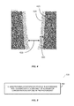
- FIG. 4 depicts a cross-section of developed resist profile that may use embodiments of the present invention.
- FIG. 5 depicts a flowchart for characterizing a photoresist profile in accordance with a magnitude of a gradient of an inhibitor concentration disposed in the photoresist, in accordance with embodiments of the present invention.
- FIG. 6 is a block diagram of a computer system that may incorporate embodiments of the present invention.
- Embodiments of the present invention address such stringent modeling and computational needs for simulating, using a computer, the lithographic photoresist chemistry, including the process steps of photo-exposure, resist baking and then development.
- a compact mathematical model is desired to represent the complex nonlinear responses of photoresist, hereinafter also referred to as “resist,” both accurately and efficiently.
- the number of modeling terms should be minimized in order to achieve good numerical efficiency, which however imposes a challenge to model completeness, namely, a compact model should have enough terms and varieties of terms to fully capture the multitude of physical and or chemical parameters and mechanisms involved in the complex process.
- the method of physical rationalization has the advantage of improving model accuracy and numerical efficiency while minimizing the number of modeling terms.
- “Physically rationalizing” and “physical rationalization” refer to the method and steps of deriving modeling terms in a compact and succinct mathematical form with adjustable and physically meaningful parameters, based on physical considerations and mathematical analyses.
- FIG. 1 depicts simplified exemplary steps 101 in the design and fabrication of an integrated circuit that may use embodiments of the present invention.
- the process starts with a product idea 100 , which is realized using Electronic Design Automation (EDA) software 110 .
- Chips 170 can be produced from the finalized design by performing fabrication 150 and packaging and assembly 160 steps.
- EDA software 110 An exemplary design flow that uses EDA software 110 is described below for illustration purposes only. For example, an actual integrated circuit design may require a designer to perform the design flow steps in a different sequence than the sequence described below.
- HDL Hardware Description Language
- the HDL code can be translated to a netlist, which can be optimized for the target technology. Further, tests can be designed and implemented to check the finished chips.
- the netlist verification 118 the netlist can be checked for compliance with timing constraints and for correspondence with the HDL code.
- an overall floor plan for the chip can be constructed and analyzed for timing and top-level routing.
- placement and routing can be performed.
- the circuit functionality can be verified at a transistor level.
- the design can be checked to correct any functional, manufacturing, electrical, or lithographic issues.
- the resolution enhancement 128 geometric manipulations can be performed on the layout to improve manufacturability of the design.
- the design can be taped-out 140 for production of masks to produce finished chips.
- the embodiments of the present invention may be used, for example in conjunction with other EDA tools at the steps of either physical verification 126 and/or mask data preparation 130 .
- embodiments of the models of photoresist processing presented herein may be used along with mask layout data when the computer is invoked to simulate the resulting pattern in the photoresist after exposure, post exposure bake and development during the semiconductor process flow.
- the results of this photoresist computer modeling which may include a characterized photoresist profile, may be applied to reduce a distortion in a printed photoresist pattern caused by a response of the photoresist to an electromagnetic wave and/or a particle beam.
- the distortion may be reduced by adjusting the layout pattern.
- the distortion may be reduced by changing the characteristics of the photoresist process.
- Embodiments of the present invention present a method of representing the behavior and response of photoresist by a compact model consisting of physically rationalized modeling terms, which is amenable to rapidly convergent parameter calibration with measured data and is well suited for fast simulations over the entire surface area of a large semiconductor chip.
- the method starts from a first step of identifying essential mechanisms and parameters that affect and contribute to the variations of the final results of developed photoresist critical dimensions (CDs) and topography profile.
- CDs photoresist critical dimensions
- topography profile the underlying physics and chemistry of each essential mechanism is analyzed, identifying the signal excitation-response relationship and the governing mathematical equations.
- a third step uses techniques of mathematical analysis including dimensional, scaling, and asymptotic analyses, extracting compact, descriptive, and parameterized modeling terms that capture the relationship between the essential mechanisms and parameters that affect the final results of developed photoresist.
- the method concludes with a fourth step of incorporating the modeling terms into a general model form.
- the obtained general model form constitutes a compact model that consists of physically rationalized modeling terms.
- the compact model itself becomes very much physical, in comparison to known mostly empirical model forms.
- One immediate advantage of the physics-based model forms derived in accordance with the four steps described above is better model stability under uncertainties or fluctuations of conditions and parameters of the modeled process, and relatedly, stronger predictive power when the models are extrapolated into process conditions and parameters outside the regions where they are calibrated, in comparison to known mostly empirical model forms.
- a linear functional of O(x,y), namely a convolution of O(x,y) with a kernel function K(x,y), is added to the signal field to capture certain pattern density-dependent effects, such as optical flare.
- Optical flare may be caused by the random scattering of light by irregularities on the photo-mask, dusts on the pellicle, and inherent microscopic density fluctuations in the glass materials of optical lenses.
- the optical intensity is often blurred by a suitable diffusion kernel G(x,y) to qualitatively represent the effects of photo-acid diffusion in the processed photoresist, ultra-violet (UV) source laser bandwidth, and/or stage vibration-induced blurring.
- ⁇ S[I(x,y)] has been referred to as a “variable threshold”, and equation (4) has been called a “variable threshold” model form, because, effectively, ⁇ S[I(x,y)], when moved to the left-hand side of equation (4), amounts to adjusting the threshold level at each specific location (x,y), in accordance with the signal distribution in its spatial neighborhood.
- variable threshold compact model evolved slightly, to employ a substantially predetermined ad-hoc empirical mathematical expression for ⁇ S[I(x,y)], namely, a predetermined model form, where a typical known recipe involves using a number of predetermined mathematical kernels from a set of orthogonal basis functions, convolving the signal I(x,y) with each of the predetermined mathematical kernels, and finally forming a linear combination of the convolution results weighted by tunable coefficients to represent the “variable threshold” ⁇ S[I(x,y)].
- the “convolution with predetermined mathematical kernels” approach generalizes the previous method that involves explicit derivatives of the signal field, because derivatives may be approximated by convolutions with suitable kernels.
- variable threshold of known compact models are empirical in nature, where the introduction and selection of the predetermined mathematical kernels are not based on specific physical/chemical steps, mechanisms, or parameters, rather, they are largely arbitrary and mostly out of mathematical or numerical convenience, reflecting merely, in a broad sense, the empirical observation that the developed resist contours or CDs are not completely determined by the on-site optical intensity, but show dependence on the signal distribution in a spatial neighborhood.
- Such known empirical “variable threshold” models have worked in the past for multiple generations or technology nodes of semiconductor manufacturing technology. But the empirical nature of such known models severely limits the model stability under uncertainties or fluctuations of conditions and parameters of the modeled process and curtails the model predictive power when extending to process conditions and parameters outside the regions where the models are calibrated.
- the empirical models often require greatly more measurement data to calibrate, and the calibration procedure takes too long to converge or does not converge at all, because the model optimizer has to search for the optimal solution over a very high-dimensional parameter space that is filled with “local optimum traps” or undesired solutions.
- FIG. 2 depicts a simplified flowchart to derive a general model form that includes physically rationalized modeling terms, in accordance with one embodiment of the present invention.
- the flowchart may include four generalized steps. In the first step, essential mechanisms and parameters are identified 202 that affect and contribute to the variations of the final results of developed photoresist critical dimensions (CDs) and topography profile;
- CDs photoresist critical dimensions
- the underlying physics and chemistry of most essential mechanisms are analyzed 204 , and the signal excitation-response relationship and the governing mathematical equations are identified.
- techniques of mathematical analysis including dimensional, scaling, and asymptotic analyses, are used to extract compact, descriptive, and parameterized modeling terms that capture the relationship between the essential mechanisms and parameters that affect the final results of developed photoresist.
- the modeling terms are incorporated into a general model form.
- the general form is a linear combination of the modeling terms.
- the general model form consists of products of the modeling terms.
- the computer-implemented method includes characterizing, using the computer, the photoresist profile in accordance with the inhibitor concentration disposed in the photoresist.
- Photoresist may further include photo-acid generators and quenchers responsive to electromagnetic radiation such as ultra-violet light or electron beams.
- the photo-exposure step may be treated as an exponential depletion of photo-acid generators and creation of photo-acids as explained in further detail below.
- the photo-acid and quencher base reaction-diffusion process may be well approximated by a “split step” algorithm, where each “split step” is either “diffusion only without nonlinearity” or “nonlinear only without diffusion”, both of which are amenable to efficient computer computation.
- FIG. 4 depicts a cross-section of developed resist profile that may use embodiments of the present invention, where the dark grey color represents the “development resistant” region of the photoresist 410 .
- the white and gapped region 420 represents the quickly developable portion of the photoresist or in other words the CD given by the pure inhibitor threshold model or the pure optical model.
- the relatively narrow light grey-colored layer 430 experiences slow development and consumes the majority of the development time, with the arrow representing the portion of the development path 440 that is within the layer 430 .
- the development rate can be modeled by:
- R ⁇ ( M ) R ma ⁇ ⁇ x ⁇ ( a + 1 ) ⁇ ( 1 - M ) n a + ( 1 - M ) n + R m ⁇ ⁇ i ⁇ ⁇ n , ( 8 ) for a positive tone development (PTD) resist, and given by:
- R ⁇ ( M ) R ma ⁇ ⁇ x ⁇ ( a + 1 ) ⁇ M n a + M n + R m ⁇ ⁇ i ⁇ ⁇ n , ( 9 ) for an NTD photoresist, where ⁇ is a constant related to the threshold M th and n is the development reaction order parameter.
- the development rate is asymptotically given by: R ( M ) ⁇ R max M n + R min , (10) which scales as M raised to the nth power.
- the computer-implemented method includes characterizing, using the computer, the photoresist profile in accordance with the inhibitor concentration raised to a power of n, wherein n is a real number greater than or equal to 5.
- n is generally a large number, which may be generally measured between 5 to 30.
- M(x,y) incorporates the effects of photo-acid and quencher diffusion
- FIG. 5 depicts a flowchart for characterizing, using the computer, a photoresist profile in accordance with a magnitude of a gradient of an inhibitor concentration disposed in the photoresist, in accordance with embodiments of the present invention, as described by equations (5), (6), and (11) above.
- the inhibitor density M(x,y) itself in equation (5) is physically rationalized into compact modeling terms, by physically and mathematically analyzing the photo-exposure and PEB steps.
- H 0 ( x,y ) [PAG] ⁇ 1 ⁇ exp[ ⁇ C Dill I ( x,y )] ⁇ , (14) where [PAG] is the concentration of the photo-acid generator.
- H ( x,y ) max ⁇ G H ( x,y )*max[ H 0 ( x,y ) ⁇ B 0 ,0] ⁇ G B ( x,y )*max[B 0 ⁇ H 0 ( x,y ),0],0 ⁇ ,
- the experimentally observed effect of photo-decomposable quencher (PDQ) that is disposed in the photoresist is identified, and the physical rationalization of a corresponding modeling term is derived as follows.
- the photo-decomposable quencher absorbs light energy and becomes decomposed, the photo-decomposition products are assumed inactive and not to affect the photo-acid and the relevant chemical reactions.
- the photo-decomposed quencher loses the capability to neutralize photo-acids. Therefore, in brightly exposed regions where a high concentration of photo-acid is generated, the PDQ is also largely decomposed and depleted, so there is less quencher remaining to neutralize the photo-acid.
- One option is to clip the photo-acid latent image following Dill's formula of photo-exposure by a suitable threshold value, and neglect the photo-acid altogether in regions below the threshold, under the physical rationalization that a low-level concentration of photo-acid is completely overwhelmed by a high initial concentration of quencher base. Only for regions with a photo-acid concentration above the threshold, the photo-acid is assumed to overcome the depleted quencher base concentration and actively catalyze the inhibitor de-blocking while diffusing in space.
- Another option is to simply square the photo-acid latent image, or raise the photo-acid concentration to a power greater than 1.
- each option above representing nonlinear contrast enhancement effect may be to incorporate a nonlinear, e.g. super-linear, scaling of the photo-acid concentration against the optical intensity, in order to represent and approximate the nonlinear enhancement of contrast, due to the photo-decomposition of quencher in conjunction with the canonical process of photo-acid generation.
- a nonlinear e.g. super-linear
- scaling of the photo-acid concentration against the optical intensity in order to represent and approximate the nonlinear enhancement of contrast, due to the photo-decomposition of quencher in conjunction with the canonical process of photo-acid generation.
- equations (17), (18), and (19) provides one compact and efficiently computable modeling term entering equation (5) as the model signal, which is physically rationalized to represent the inhibitor concentration after the steps of photo-exposure and PEB. Therefore in one embodiment the inhibitor concentration includes a natural exponential function of a photo-acid concentration disposed in the photoresist.
- the photo-acid concentration H(x,y) in equation (12) or (15) incorporates another modeling term that is physically rationalized to represent the so-called “chemical flare” effect, which refers to the transfer of photo-acid from high concentration regions to relatively low concentration regions, via the complex process of gaseous flow of photo-acid out of the photoresist film into the chamber of the PEB oven, gaseous diffusion in the chamber of the PEB oven, and subsequent re-deposition onto and being absorbed back into the photoresist film.
- the physically rationalized modeling terms ⁇ H(x,y) and ⁇ B(x,y) may be incorporated into, for example, equation (19) as additive terms to H(x,y), so to obtain a physically rationalized modeling term for the inhibitor concentration:
- M ( x,y ) exp ⁇ C CAR ⁇ [H ( x,y )+ ⁇ H ( x,y ) ⁇ B ( x,y )] ⁇ , (24) with H(x,y), ⁇ H(x,y), and ⁇ B(x,y) defined in equations (18), (20) or (21), and (22) or (23) respectively.
- the physically rationalized modeling term of M(x,y) of equation (24) in turn enters the physics-based compact model form of equation (5).
- the effect of time-varying and photoresist opening aperture size-dependent development rate for the lower portion of the photoresist film closer to the wafer substrate is identified.
- the development rate may be analyzed in accordance with the mass transport limitation, namely, limited rates of mass transport for development agents from the bulk of the developer solution to the lower portion of the photoresist film through the already-opened apertures in the photoresist film, and for dissolved photoresist materials to flow out of the apertures and into the bulk of the developer solution.
- the mass transport-limited development rate should be a product of the bulk development rate R(M) and the aperture-size limited rate of mass transport R′[A(x,y)], with A(x,y) being an aperture density function, representing the effective aperture size as seen by a point (x,y) in the lower portion of the photoresist film.
- an aperture density function can be obtained by convolving the intended photoresist pattern or simulated developed photoresist contours in the top portion of the photoresist film with a suitable weighting kernel, which represents a weighted area of photoresist opening aperture in the upper portion of the photoresist film with respect to the point (x,y) in the lower portion of the photoresist film.
- the aperture density function may be computed as a weighted integration over the area of the intended photoresist pattern or simulated developed photoresist contours in the top portion of the photoresist film that is “visible” to the point (x,y) in the lower portion of the photoresist film, namely, the weighted integration accumulates weighted area only over locations of photoresist opening that are connected with the point (x,y) through a “line of sight.” Therefore, any location of photoresist opening that has the straight line pointing to the point (x,y) obstructed by undeveloped photoresist may not contribute to the weighted integration.
- FIG. 6 is a block diagram of a computer system that may incorporate embodiments of the present invention.
- FIG. 6 is merely illustrative of an embodiment incorporating the present invention and does not limit the scope of the invention as recited in the claims.
- One of ordinary skill in the art would recognize other variations, modifications, and alternatives.
- computer system 600 typically includes a monitor 610 , a computer 620 , user output devices 630 , user input devices 640 , communications interface 650 , and the like.
- computer 620 may include a processor(s) 660 that communicates with a number of peripheral devices via a bus subsystem 690 .
- peripheral devices may include user output devices 630 , user input devices 640 , communications interface 650 , and a storage subsystem, such as random access memory (RAM) 670 and disk drive 680 .
- RAM random access memory
- User input devices 630 include all possible types of devices and mechanisms for inputting information to computer system 620 . These may include a keyboard, a keypad, a touch screen incorporated into the display, audio input devices such as voice recognition systems, microphones, and other types of input devices. In various embodiments, user input devices 630 are typically embodied as a computer mouse, a trackball, a track pad, a joystick, wireless remote, drawing tablet, voice command system, eye tracking system, and the like. User input devices 630 typically allow a user to select objects, icons, text and the like that appear on the monitor 610 via a command such as a click of a button or the like.
- User output devices 640 include all possible types of devices and mechanisms for outputting information from computer 620 . These may include a display (e.g., monitor 610 ), non-visual displays such as audio output devices, etc.
- Communications interface 650 provides an interface to other communication networks and devices. Communications interface 650 may serve as an interface for receiving data from and transmitting data to other systems.
- Embodiments of communications interface 650 typically include an Ethernet card, a modem (telephone, satellite, cable, ISDN), (asynchronous) digital subscriber line (DSL) unit, FireWire interface, USB interface, and the like.
- communications interface 650 may be coupled to a computer network, to a FireWire bus, or the like.
- communications interfaces 650 may be physically integrated on the motherboard of computer 620 , and may be a software program, such as soft DSL, or the like.
- computer system 600 may also include software that enables communications over a network such as the HTTP, TCP/IP, RTP/RTSP protocols, and the like.
- software that enables communications over a network
- HTTP HyperText Transfer Protocol
- TCP/IP Transmission Control Protocol
- RTP/RTSP protocols Remote Method Protocol
- other communications software and transfer protocols may also be used, for example IPX, UDP or the like.
- computer 620 includes one or more Xeon microprocessors from Intel as processor(s) 660 . Further, one embodiment, computer 620 includes a UNIX-based operating system.
- RAM 670 and disk drive 680 are examples of tangible media configured to store data such as embodiments of the present invention, including executable computer code, human readable code, or the like.
- Other types of tangible media include floppy disks, removable hard disks, optical storage media such as CD-ROMS, DVDs and bar codes, semiconductor memories such as flash memories, non-transitory read-only-memories (ROMS), battery-backed volatile memories, networked storage devices, and the like.
- RAM 670 and disk drive 680 may be configured to store the basic programming and data constructs that provide the functionality of the present invention.
- RAM 670 and disk drive 680 Software code modules and instructions that provide the functionality of the present invention may be stored in RAM 670 and disk drive 680 . These software modules may be executed by processor(s) 660 . RAM 670 and disk drive 680 may also provide a repository for storing data used in accordance with the present invention.
- RAM 670 and disk drive 680 may include a number of memories including a main random access memory (RAM) for storage of instructions and data during program execution and a read only memory (ROM) in which fixed non-transitory instructions are stored.
- RAM 670 and disk drive 680 may include a file storage subsystem providing persistent (non-volatile) storage for program and data files.
- RAM 670 and disk drive 680 may also include removable storage systems, such as removable flash memory.
- Bus subsystem 690 provides a mechanism for letting the various components and subsystems of computer 620 communicate with each other as intended. Although bus subsystem 690 is shown schematically as a single bus, alternative embodiments of the bus subsystem may utilize multiple busses.
- FIG. 6 is representative of a computer system capable of embodying the present invention. It will be readily apparent to one of ordinary skill in the art that many other hardware and software configurations are suitable for use with the present invention.
- the computer may be a desktop, portable, rack-mounted or tablet configuration.
- the computer may be a series of networked computers.
- other microprocessors are contemplated, such as PentiumTM or ItaniumTM microprocessors; OpteronTM or AthlonXPTM microprocessors from Advanced Micro Devices, Inc; and the like.
- Various embodiments of the present invention can be implemented in the form of logic in software or hardware or a combination of both.
- the logic may be stored in a computer readable or machine-readable non-transitory storage medium as a set of instructions adapted to direct a processor of a computer system to perform a set of steps disclosed in embodiments of the present invention.
- the logic may form part of a computer program product adapted to direct an information-processing device to perform a set of steps disclosed in embodiments of the present invention. Based on the disclosure and teachings provided herein, a person of ordinary skill in the art will appreciate other ways and/or methods to implement the present invention.
- a computer-readable storage medium includes, but is not limited to, volatile memory, non-volatile memory, magnetic and optical storage devices such as disk drives, magnetic tape, CDs (compact discs), DVDs (digital versatile discs or digital video discs), or other media, now known or later developed, that are capable of storing code and/or data.
- Hardware modules or apparatuses described herein include, but are not limited to, application-specific integrated circuits (ASICs), field-programmable gate arrays (FPGAs), dedicated or shared processors, and/or other hardware modules or apparatuses now known or later developed.
- the methods and processes described herein may be partially or fully embodied as code and/or data stored in a computer-readable storage medium or device, so that when a computer system reads and executes the code and/or data, the computer system performs the associated methods and processes.
- the methods and processes may also be partially or fully embodied in hardware modules or apparatuses, so that when the hardware modules or apparatuses are activated, they perform the associated methods and processes.
- the methods and processes disclosed herein may be embodied using a combination of code, data, and hardware modules or apparatuses.
- the above embodiments of the present invention are illustrative and not limiting. Various alternatives and equivalents are possible.
- the invention has been described with reference to inhibitor concentration by way of an example, it is understood that the invention is not limited by the inhibitor concentration but may also be applicable to model forms based on a different physical or mathematical quantity as the model signal such as the optical intensity, the photo-acid concentration, the chemically amplified inhibitor de-blocking concentration or its complement, a resist development solubility measure depending on the photo-acid concentration or the optical intensity directly, and ultimately the spatial distribution of resist development time.
- EDA electronic design automation
Landscapes
- Physics & Mathematics (AREA)
- General Physics & Mathematics (AREA)
- Spectroscopy & Molecular Physics (AREA)
- Exposure And Positioning Against Photoresist Photosensitive Materials (AREA)
- Engineering & Computer Science (AREA)
- Computer Hardware Design (AREA)
- Theoretical Computer Science (AREA)
- Evolutionary Computation (AREA)
- Geometry (AREA)
- General Engineering & Computer Science (AREA)
- Photosensitive Polymer And Photoresist Processing (AREA)
Abstract
Description
S th =S[O(x,y), P], (1)
in order to produce the desired contour or CD predictions.
I(x,y)=
where the potentially P-dependent TCC is a linear operator corresponding to the so-called transmission cross coefficients. Sometimes a linear functional of O(x,y), namely a convolution of O(x,y) with a kernel function K(x,y), is added to the signal field to capture certain pattern density-dependent effects, such as optical flare. Optical flare may be caused by the random scattering of light by irregularities on the photo-mask, dusts on the pellicle, and inherent microscopic density fluctuations in the glass materials of optical lenses. Furthermore, the optical intensity is often blurred by a suitable diffusion kernel G(x,y) to qualitatively represent the effects of photo-acid diffusion in the processed photoresist, ultra-violet (UV) source laser bandwidth, and/or stage vibration-induced blurring. The model equation thus becomes:
I th =G(x,y)*I(x,y)+K(x,y)*O(x,y), (3)
with I(x,y) defined in equation (2) above.
S th =G(x,y)*I(x,y)+K(x,y)*O(x,y)+ΔS[I(x,y)], (4)
where ΔS is a functional of the optical intensity I(x,y), and a shorthand for typically a collection of modeling terms associated respectively with the absolute value of the slope, the second-order derivatives (e.g., the Laplacian), and other derived quantities of the signal field I(x,y). Such ΔS[I(x,y)] has been referred to as a “variable threshold”, and equation (4) has been called a “variable threshold” model form, because, effectively, ΔS[I(x,y)], when moved to the left-hand side of equation (4), amounts to adjusting the threshold level at each specific location (x,y), in accordance with the signal distribution in its spatial neighborhood.
M th =M(x,y)+ΔM(x,y), (5)
where Mth is a constant threshold applied to the model signal field to extract predicted or simulated contours or CDs of the developed resist pattern or topography, i.e. a thresholding operation, and where ΔM(x,y) represents a collection of modeling terms called “variable biases”. Equation (5) chooses the inhibitor density M(x,y) as the model signal field, because both the photo-exposure and the PEB steps are treated rigorously, or nearly rigorously, via whole-field signal processing algorithms. Therefore in one embodiment, the computer-implemented method includes characterizing, using the computer, the photoresist profile in accordance with the inhibitor concentration disposed in the photoresist. Photoresist may further include photo-acid generators and quenchers responsive to electromagnetic radiation such as ultra-violet light or electron beams. The photo-exposure step may be treated as an exponential depletion of photo-acid generators and creation of photo-acids as explained in further detail below. The photo-acid and quencher base reaction-diffusion process may be well approximated by a “split step” algorithm, where each “split step” is either “diffusion only without nonlinearity” or “nonlinear only without diffusion”, both of which are amenable to efficient computer computation.
ΔM(x,y)=|∇M(x,y)|×ΔCD(x,y), (6)
which in other words is the change needed to the inhibitor model to get the resist process model signal.
ΔCD(x,y)=R[M(x,y)]×ΔT, (7)
with ΔT being most of the development time, thus substantially the same and independent of the lithography patterns.
for a positive tone development (PTD) resist, and given by:
for an NTD photoresist, where α is a constant related to the threshold Mth and n is the development reaction order parameter. For an NTD photoresist and α»1 in particular, the development rate is asymptotically given by:
R(M)≈R max M n+R min, (10)
which scales as M raised to the nth power. Combining all results of the asymptotic, dimensional, and scaling analyses, a physically rationalized modeling term of variable bias is obtained to represent the effect of development bias:
ΔM(x,y)=C×|∇M(x,y)|×[M(x,y)]n (11)
with C and n being calibration parameters. The physical rationalization also informs that C is related to the product RmaxΔT and n is related to the development reaction order. Therefore in one embodiment, the computer-implemented method includes characterizing, using the computer, the photoresist profile in accordance with the inhibitor concentration raised to a power of n, wherein n is a real number greater than or equal to 5.
H(x,y)=max{G H(x,y)*max[C Dill I(x,y)−B 0, 0]−G B(x,y)*max[B 0 −C Dill I(x,y),0],0}. (12)
M(x,y)=exp[−C CAR H(x,y)]=exp[−C CAR×max{G H(x,y)*max[C Dill I(x,y)−B 0,0]−G B(x,y)*max[B 0 −C Dill I(x,y),0],0}], (13)
where CCAR is a parameter proportional to the reaction rate of the chemically amplified inhibitor deblocking process. Alternatively, the “Dill C” photo-exposure step is treated rigorously to get an initial photo-acid concentration:
H 0(x,y)=[PAG]{1−exp[−C Dill I(x,y)]}, (14)
where [PAG] is the concentration of the photo-acid generator. The diffusion, acid-base neutralization, and chemical amplification processes are treated with the same physical rationalizations as above, so to obtain:
H(x,y)=max{G H(x,y)*max[H 0(x,y)−B 0,0]−G B(x,y)*max[B0 −H 0(x,y),0],0}, (15)
and
M(x,y)=exp[−C CAR H(x,y)]=exp[−C CAR×max{G H(x,y)*max[H 0(x,y)−B 0,0]−G B(x,y)*max[B 0 −H 0(x,y),0],0}]. (16)
B 0(x,y)=[BASE]exp[−C Dill,Base I(x,y)], (17)
where [BASE] is the initial quencher base concentration before photo-exposure, and CDill,Base is a “Dill C” parameter representing the rate of photo-absorption and photo-decomposition of the quencher base under photo-exposure. Consequently, equations (15) and (16) may be augmented and physically rationalized as:
H(x,y)=max{G H(x,y)*max[H 0(x,y)−B 0(x,y),0]−G B(x,y)*max[B 0(x,y)−H 0(x,y),0],0}, (18)
M(x,y)=exp[−C CAR H(x,y)]=exp[−C CAR×max{G H(x,y)*max[H 0(x,y)−B 0(x,y),0]−G B(x,y)*max[B 0(x,y)−H 0(x,y),0],0}], (19)
with B0(x,y) defined as in equation (17).
ΔH(x,y)=G ChemicalFlare(x,y)*max[C Dill I(x,y)−B 0(x,y),0] (20)
or
ΔH(x,y)=G ChemicalFlare(x,y)*max[H 0(x,y)−B 0(x,y),0] (21)
may be incorporated into H(x,y) in equation (12) or (15) additively, where the Gaussian convolution kernel GChemicalFlare(x,y) has a diffusion length that is substantially larger than that of GH(x,y), reflecting the gaseous diffusion nature of “chemical flare”. Similarly, there is also a “chemical flare” effect for the quencher base, referring to the often longer-ranged diffusion of quencher base via the steps of gaseous out-flow from the photoresist film, gaseous diffusion, and re-deposition back into the photoresist film of quencher base. Such “chemical flare” effect of the quencher base is similarly physically rationalized into a modeling term:
ΔB(x,y)=G′ ChemicalFlare(x,y)*max[B 0(x,y)−CDill I(x,y),0], (22)
or
ΔB(x,y)=G′ ChemicalFlare(x,y)*max[B 0(x,y)−H 0(x,y),0], (23)
where the Gaussian convolution kernel G′ChemicalFlare(x,y) has a diffusion length that is substantially larger than that of GB(x,y), reflecting the gaseous diffusion nature of “chemical flare” associated with the quencher base. The physically rationalized modeling terms ΔH(x,y) and ΔB(x,y) may be incorporated into, for example, equation (19) as additive terms to H(x,y), so to obtain a physically rationalized modeling term for the inhibitor concentration:
M(x,y)=exp{−C CAR ×[H(x,y)+ΔH(x,y)−ΔB(x,y)]}, (24)
with H(x,y), ΔH(x,y), and ΔB(x,y) defined in equations (18), (20) or (21), and (22) or (23) respectively. The physically rationalized modeling term of M(x,y) of equation (24) in turn enters the physics-based compact model form of equation (5).
R′[A(x,y)]=R′ 0 −R′ 1 A(x,y)+R′ 2 [A(x,y)]2+ (25)
With the second- and higher-order terms in equation (25) neglected, the mass transport-limited development rate reads:
R′[A(x,y)]R[M(x,y)]=R′ 0 R[M(x,y)]−R′ 1 A(x,y)R[M(x,y)]. (26)
The first term on the right-hand side of equation (26) coincides with the physically rationalized modeling term of variable bias as given by equation (11), whereas the second term on the right-hand side of equation (26), when combined with equations (6), (7), and (10), produces another physically rationalized modeling term of variable bias
ΔM 2(x,y)=−C×A(x,y)×|∇M(x,y)|×[M(x,y)]n, (27)
which represents the photoresist aperture-induced development bias, and enters equation (5) as another additive term to the ΔM(x,y) collection of variable biases.
Claims (24)
Priority Applications (1)
| Application Number | Priority Date | Filing Date | Title |
|---|---|---|---|
| US14/789,948 US10386718B2 (en) | 2014-07-11 | 2015-07-01 | Method for modeling a photoresist profile |
Applications Claiming Priority (2)
| Application Number | Priority Date | Filing Date | Title |
|---|---|---|---|
| US201462023551P | 2014-07-11 | 2014-07-11 | |
| US14/789,948 US10386718B2 (en) | 2014-07-11 | 2015-07-01 | Method for modeling a photoresist profile |
Publications (2)
| Publication Number | Publication Date |
|---|---|
| US20160012175A1 US20160012175A1 (en) | 2016-01-14 |
| US10386718B2 true US10386718B2 (en) | 2019-08-20 |
Family
ID=55067775
Family Applications (1)
| Application Number | Title | Priority Date | Filing Date |
|---|---|---|---|
| US14/789,948 Active US10386718B2 (en) | 2014-07-11 | 2015-07-01 | Method for modeling a photoresist profile |
Country Status (3)
| Country | Link |
|---|---|
| US (1) | US10386718B2 (en) |
| KR (1) | KR102438831B1 (en) |
| TW (1) | TWI703404B (en) |
Families Citing this family (4)
| Publication number | Priority date | Publication date | Assignee | Title |
|---|---|---|---|---|
| US10901322B2 (en) | 2017-05-12 | 2021-01-26 | Asml Netherlands B.V. | Methods for evaluating resist development |
| US11493850B2 (en) | 2019-07-23 | 2022-11-08 | Samsung Electronics Co., Ltd. | Lithography method using multi-scale simulation, semiconductor device manufacturing method and exposure equipment |
| KR20220149823A (en) * | 2021-04-30 | 2022-11-09 | 삼성전자주식회사 | Lithography method using multi-scale simulation, and method of manufacturing semiconductor device and exposure equipment based on the lithography method |
| US20230222264A1 (en) * | 2022-01-07 | 2023-07-13 | Applied Materials, Inc. | Processing chamber calibration |
Citations (5)
| Publication number | Priority date | Publication date | Assignee | Title |
|---|---|---|---|---|
| US5889686A (en) * | 1996-08-22 | 1999-03-30 | Kabushiki Kaisha Toshiba | Profile simulation method |
| US5999720A (en) * | 1997-02-06 | 1999-12-07 | Nec Corporation | Post exposure bake simulation method |
| US20070282574A1 (en) * | 2006-05-31 | 2007-12-06 | Jensheng Huang | Method and apparatus for determining a process model that models the impact of CAR/PEB on the resist profile |
| US20120079436A1 (en) * | 2010-09-29 | 2012-03-29 | Nikon Corporation | Fast photoresist model |
| US9733576B2 (en) * | 2014-03-17 | 2017-08-15 | Kla-Tencor Corporation | Model for accurate photoresist profile prediction |
Family Cites Families (3)
| Publication number | Priority date | Publication date | Assignee | Title |
|---|---|---|---|---|
| EP1688795A3 (en) * | 2005-01-28 | 2007-12-12 | ASML MaskTools B.V. | Method, computer program and apparatus for improving calibration of resist models used in critical dimension calculation |
| JP4737426B2 (en) * | 2006-04-21 | 2011-08-03 | 信越化学工業株式会社 | Photomask blank |
| US8555209B2 (en) * | 2011-02-04 | 2013-10-08 | Samsung Electronics Co., Ltd. | Method for fabricating a semiconductor device using a modeling algorithm to model the proximity effect from the sub-layer |
-
2015
- 2015-07-01 US US14/789,948 patent/US10386718B2/en active Active
- 2015-07-09 TW TW104122424A patent/TWI703404B/en active
- 2015-07-10 KR KR1020150098418A patent/KR102438831B1/en active Active
Patent Citations (6)
| Publication number | Priority date | Publication date | Assignee | Title |
|---|---|---|---|---|
| US5889686A (en) * | 1996-08-22 | 1999-03-30 | Kabushiki Kaisha Toshiba | Profile simulation method |
| US5999720A (en) * | 1997-02-06 | 1999-12-07 | Nec Corporation | Post exposure bake simulation method |
| US20070282574A1 (en) * | 2006-05-31 | 2007-12-06 | Jensheng Huang | Method and apparatus for determining a process model that models the impact of CAR/PEB on the resist profile |
| US20120079436A1 (en) * | 2010-09-29 | 2012-03-29 | Nikon Corporation | Fast photoresist model |
| US8910093B2 (en) * | 2010-09-29 | 2014-12-09 | Nikon Corporation | Fast photoresist model |
| US9733576B2 (en) * | 2014-03-17 | 2017-08-15 | Kla-Tencor Corporation | Model for accurate photoresist profile prediction |
Non-Patent Citations (1)
| Title |
|---|
| Sean Burns, The Effect of Electrostatic Surface Charger on Photoresist Dissolution, Apr. 2000, pp. 1-28. * |
Also Published As
| Publication number | Publication date |
|---|---|
| KR102438831B1 (en) | 2022-09-01 |
| TW201614530A (en) | 2016-04-16 |
| US20160012175A1 (en) | 2016-01-14 |
| TWI703404B (en) | 2020-09-01 |
| KR20160007434A (en) | 2016-01-20 |
Similar Documents
| Publication | Publication Date | Title |
|---|---|---|
| US11061318B2 (en) | Lithography model calibration | |
| TWI621957B (en) | Sub-resolution assist feature implementation using shot optimization | |
| US11061373B1 (en) | Method and system for calculating probability of success or failure for a lithographic process due to stochastic variations of the lithographic process | |
| US11415897B2 (en) | Calibrating stochastic signals in compact modeling | |
| US8473271B2 (en) | Fast photolithography process simulation to predict remaining resist thickness | |
| US20100191518A1 (en) | Compact abbe's kernel generation using principal component analysis | |
| US20090276749A1 (en) | Gate modeling for semiconductor fabrication process effects | |
| TWI767340B (en) | Lithography improvement based on defect probability distributions and critical dimension variations | |
| US10386718B2 (en) | Method for modeling a photoresist profile | |
| KR20230098783A (en) | Stochastic Aware Lithography Models for Mask Synthesis | |
| US11468222B2 (en) | Stochastic signal prediction in compact modeling | |
| US10852635B2 (en) | Compact modeling for the negative tone development processes | |
| US8006203B2 (en) | Bulk image modeling for optical proximity correction | |
| US20160363854A1 (en) | Pattern Optical Similarity Determination | |
| US10120963B1 (en) | Figurative models calibrated to correct errors in process models | |
| US11270054B1 (en) | Method and system for calculating printed area metric indicative of stochastic variations of the lithographic process | |
| KR102936955B1 (en) | Lithography improvements based on defect probability distributions and critical dimension variations. | |
| TWI859348B (en) | Method, non-transitory computer readable storage medium and apparatus for predicting defect rate based on lithographic model parameters | |
| US12474634B2 (en) | Mask synthesis integrating mask fabrication effects and wafer lithography effects | |
| Lam et al. | Nebulous hotspot and algorithm variability in computation lithography | |
| US20260064012A1 (en) | Method and system for three-dimensional modeling of stochastic variations of lithographic process | |
| Gupta et al. | Modeling edge placement error distribution in standard cell library | |
| CN119623401B (en) | Method for establishing OPC model, electronic device, storage medium and program product | |
| TWI920165B (en) | Method, system and non-transitory computer readable medium utilizing stochastic-aware lithographic models for mask synthesis | |
| JP2024539821A (en) | Mask fabrication effects in 3D mask simulation using feature images |
Legal Events
| Date | Code | Title | Description |
|---|---|---|---|
| STPP | Information on status: patent application and granting procedure in general |
Free format text: NON FINAL ACTION MAILED |
|
| STPP | Information on status: patent application and granting procedure in general |
Free format text: NOTICE OF ALLOWANCE MAILED -- APPLICATION RECEIVED IN OFFICE OF PUBLICATIONS |
|
| AS | Assignment |
Owner name: SYNOPSYS, INC., CALIFORNIA Free format text: ASSIGNMENT OF ASSIGNORS INTEREST;ASSIGNORS:WU, CHENG EN;WEI, HAIQING;ZHANG, QIAOLIN;AND OTHERS;SIGNING DATES FROM 20190522 TO 20190523;REEL/FRAME:049505/0171 |
|
| STPP | Information on status: patent application and granting procedure in general |
Free format text: PUBLICATIONS -- ISSUE FEE PAYMENT VERIFIED |
|
| STCF | Information on status: patent grant |
Free format text: PATENTED CASE |
|
| MAFP | Maintenance fee payment |
Free format text: PAYMENT OF MAINTENANCE FEE, 4TH YEAR, LARGE ENTITY (ORIGINAL EVENT CODE: M1551); ENTITY STATUS OF PATENT OWNER: LARGE ENTITY Year of fee payment: 4 |