US10381463B2 - Patterned sidewall smoothing using a pre-smoothed inverted tone pattern - Google Patents
Patterned sidewall smoothing using a pre-smoothed inverted tone pattern Download PDFInfo
- Publication number
- US10381463B2 US10381463B2 US15/875,619 US201815875619A US10381463B2 US 10381463 B2 US10381463 B2 US 10381463B2 US 201815875619 A US201815875619 A US 201815875619A US 10381463 B2 US10381463 B2 US 10381463B2
- Authority
- US
- United States
- Prior art keywords
- patterned mask
- less
- substrate
- target layer
- smoothing
- Prior art date
- Legal status (The legal status is an assumption and is not a legal conclusion. Google has not performed a legal analysis and makes no representation as to the accuracy of the status listed.)
- Expired - Fee Related
Links
Images


Classifications
-
- H01L29/66795—
-
- H01L29/161—
-
- H01L29/785—
-
- H—ELECTRICITY
- H10—SEMICONDUCTOR DEVICES; ELECTRIC SOLID-STATE DEVICES NOT OTHERWISE PROVIDED FOR
- H10D—INORGANIC ELECTRIC SEMICONDUCTOR DEVICES
- H10D30/00—Field-effect transistors [FET]
- H10D30/01—Manufacture or treatment
- H10D30/021—Manufacture or treatment of FETs having insulated gates [IGFET]
- H10D30/024—Manufacture or treatment of FETs having insulated gates [IGFET] of fin field-effect transistors [FinFET]
-
- H—ELECTRICITY
- H10—SEMICONDUCTOR DEVICES; ELECTRIC SOLID-STATE DEVICES NOT OTHERWISE PROVIDED FOR
- H10D—INORGANIC ELECTRIC SEMICONDUCTOR DEVICES
- H10D30/00—Field-effect transistors [FET]
- H10D30/60—Insulated-gate field-effect transistors [IGFET]
- H10D30/62—Fin field-effect transistors [FinFET]
-
- H—ELECTRICITY
- H10—SEMICONDUCTOR DEVICES; ELECTRIC SOLID-STATE DEVICES NOT OTHERWISE PROVIDED FOR
- H10D—INORGANIC ELECTRIC SEMICONDUCTOR DEVICES
- H10D62/00—Semiconductor bodies, or regions thereof, of devices having potential barriers
- H10D62/80—Semiconductor bodies, or regions thereof, of devices having potential barriers characterised by the materials
- H10D62/82—Heterojunctions
- H10D62/822—Heterojunctions comprising only Group IV materials heterojunctions, e.g. Si/Ge heterojunctions
-
- H—ELECTRICITY
- H10—SEMICONDUCTOR DEVICES; ELECTRIC SOLID-STATE DEVICES NOT OTHERWISE PROVIDED FOR
- H10D—INORGANIC ELECTRIC SEMICONDUCTOR DEVICES
- H10D62/00—Semiconductor bodies, or regions thereof, of devices having potential barriers
- H10D62/80—Semiconductor bodies, or regions thereof, of devices having potential barriers characterised by the materials
- H10D62/83—Semiconductor bodies, or regions thereof, of devices having potential barriers characterised by the materials being Group IV materials, e.g. B-doped Si or undoped Ge
- H10D62/832—Semiconductor bodies, or regions thereof, of devices having potential barriers characterised by the materials being Group IV materials, e.g. B-doped Si or undoped Ge being Group IV materials comprising two or more elements, e.g. SiGe
-
- H—ELECTRICITY
- H10—SEMICONDUCTOR DEVICES; ELECTRIC SOLID-STATE DEVICES NOT OTHERWISE PROVIDED FOR
- H10D—INORGANIC ELECTRIC SEMICONDUCTOR DEVICES
- H10D84/00—Integrated devices formed in or on semiconductor substrates that comprise only semiconducting layers, e.g. on Si wafers or on GaAs-on-Si wafers
- H10D84/01—Manufacture or treatment
- H10D84/0123—Integrating together multiple components covered by H10D12/00 or H10D30/00, e.g. integrating multiple IGBTs
- H10D84/0126—Integrating together multiple components covered by H10D12/00 or H10D30/00, e.g. integrating multiple IGBTs the components including insulated gates, e.g. IGFETs
- H10D84/0165—Integrating together multiple components covered by H10D12/00 or H10D30/00, e.g. integrating multiple IGBTs the components including insulated gates, e.g. IGFETs the components including complementary IGFETs, e.g. CMOS devices
- H10D84/0193—Integrating together multiple components covered by H10D12/00 or H10D30/00, e.g. integrating multiple IGBTs the components including insulated gates, e.g. IGFETs the components including complementary IGFETs, e.g. CMOS devices the components including FinFETs
-
- H—ELECTRICITY
- H10—SEMICONDUCTOR DEVICES; ELECTRIC SOLID-STATE DEVICES NOT OTHERWISE PROVIDED FOR
- H10D—INORGANIC ELECTRIC SEMICONDUCTOR DEVICES
- H10D84/00—Integrated devices formed in or on semiconductor substrates that comprise only semiconducting layers, e.g. on Si wafers or on GaAs-on-Si wafers
- H10D84/01—Manufacture or treatment
- H10D84/02—Manufacture or treatment characterised by using material-based technologies
- H10D84/03—Manufacture or treatment characterised by using material-based technologies using Group IV technology, e.g. silicon technology or silicon-carbide [SiC] technology
- H10D84/038—Manufacture or treatment characterised by using material-based technologies using Group IV technology, e.g. silicon technology or silicon-carbide [SiC] technology using silicon technology, e.g. SiGe
-
- H—ELECTRICITY
- H10—SEMICONDUCTOR DEVICES; ELECTRIC SOLID-STATE DEVICES NOT OTHERWISE PROVIDED FOR
- H10D—INORGANIC ELECTRIC SEMICONDUCTOR DEVICES
- H10D84/00—Integrated devices formed in or on semiconductor substrates that comprise only semiconducting layers, e.g. on Si wafers or on GaAs-on-Si wafers
- H10D84/80—Integrated devices formed in or on semiconductor substrates that comprise only semiconducting layers, e.g. on Si wafers or on GaAs-on-Si wafers characterised by the integration of at least one component covered by groups H10D12/00 or H10D30/00, e.g. integration of IGFETs
- H10D84/82—Integrated devices formed in or on semiconductor substrates that comprise only semiconducting layers, e.g. on Si wafers or on GaAs-on-Si wafers characterised by the integration of at least one component covered by groups H10D12/00 or H10D30/00, e.g. integration of IGFETs of only field-effect components
- H10D84/83—Integrated devices formed in or on semiconductor substrates that comprise only semiconducting layers, e.g. on Si wafers or on GaAs-on-Si wafers characterised by the integration of at least one component covered by groups H10D12/00 or H10D30/00, e.g. integration of IGFETs of only field-effect components of only insulated-gate FETs [IGFET]
- H10D84/85—Complementary IGFETs, e.g. CMOS
- H10D84/853—Complementary IGFETs, e.g. CMOS comprising FinFETs
-
- H—ELECTRICITY
- H01—ELECTRIC ELEMENTS
- H01L—SEMICONDUCTOR DEVICES NOT COVERED BY CLASS H10
- H01L21/00—Processes or apparatus adapted for the manufacture or treatment of semiconductor or solid state devices or of parts thereof
- H01L21/02—Manufacture or treatment of semiconductor devices or of parts thereof
- H01L21/027—Making masks on semiconductor bodies for further photolithographic processing not provided for in group H01L21/18 or H01L21/34
- H01L21/033—Making masks on semiconductor bodies for further photolithographic processing not provided for in group H01L21/18 or H01L21/34 comprising inorganic layers
- H01L21/0331—Making masks on semiconductor bodies for further photolithographic processing not provided for in group H01L21/18 or H01L21/34 comprising inorganic layers for lift-off processes
-
- H10P76/403—
Definitions
- the present invention relates in general to semiconductor and optoelectronic device fabrication methods and resulting structures. More specifically, the present invention relates to fabrication methods and resulting structures for smoothing the sidewall roughness of a post-etched film.
- FETs field effect transistors
- Semiconductor optical waveguides are a very important part of modern integrated optoelectronic systems, especially for electrically active devices. Applications range from semiconductor lasers, optical filters, switches, modulators, isolators, and photodetectors. To increase device density, improve performance, and decrease the power load of these devices, device fabricators employ increasingly sophisticated fabrication techniques that include a combination of lithography, sidewall image transfer, spacer imaging and other processes to form final device structures having progressively decreasing critical dimensions.
- a method for smoothing the sidewall roughness of a post-etched film includes forming a sacrificial layer on a substrate.
- a patterned mask is formed by removing portions of the sacrificial layer to expose a surface of the substrate.
- the sidewalls of the patterned mask are smoothed, and a target layer is formed over the patterned mask and the substrate. Portions of the target layer are removed to expose a surface of the patterned mask, and the patterned mask is removed.
- a method for smoothing the sidewall roughness of a post-etched film includes forming a sacrificial layer on a substrate.
- a patterned mask is formed by removing portions of the sacrificial layer to expose a surface of the substrate. Sidewalls of the patterned mask are smoothed, and a semiconductor layer is formed over the patterned mask and the substrate.
- a semiconductor fin is formed by removing portions of the semiconductor layer to expose a surface of the patterned mask. The patterned mask is removed, and a gate is formed over a channel region of the semiconductor fin.
- a semiconductor device having smoothed sidewalls includes a semiconductor fin formed on a substrate and a gate formed over a channel region of the semiconductor fin.
- Each sidewall of the semiconductor fin includes a one sigma root-mean-square (RMS) roughness of less than about 10 atomic layers, or less than about 3 nanometers (nm).
- RMS root-mean-square
- FIG. 1 depicts a cross-sectional view of a structure having a sacrificial layer formed on a substrate during an intermediate operation of a method of fabricating a semiconductor device according to one or more embodiments of the present invention
- FIG. 2 depicts a cross-sectional view of the structure after patterning the sacrificial layer to form a patterned mask during an intermediate operation of a method of fabricating a semiconductor device according to one or more embodiments of the present invention
- FIG. 3 depicts a cross-sectional view of the structure after smoothing the sidewalls of the patterned mask during an intermediate operation of a method of fabricating a semiconductor device according to one or more embodiments of the present invention
- FIG. 4 depicts a cross-sectional view of the structure after smoothing the sidewalls of the patterned mask causes the sidewalls of the patterned mask to become tapered during an intermediate operation of a method of fabricating a semiconductor device according to one or more embodiments of the present invention
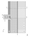
- FIG. 5 depicts a cross-sectional view of the structure after forming a target layer over the patterned mask and the substrate during an intermediate operation of a method of fabricating a semiconductor device according to one or more embodiments of the present invention
- FIG. 6 depicts a cross-sectional view of the structure after removing portions (i.e., the overburden) of the target layer to form a target structure over the substrate during an intermediate operation of a method of fabricating a semiconductor device according to one or more embodiments of the present invention
- FIG. 7 depicts a cross-sectional view of the structure after selectively removing the patterned mask from the substrate during an intermediate operation of a method of fabricating a semiconductor device according to one or more embodiments of the present invention
- FIG. 8 depicts a cross-sectional view of the structure having tapered sidewalls during an intermediate operation of a method of fabricating a semiconductor device according to one or more embodiments of the present invention
- FIG. 9 depicts a cross-sectional view of a structure along a direction X-X′ (parallel to fin direction) after forming a semiconductor fin on a substrate during an intermediate operation of a method of fabricating a semiconductor device according to one or more embodiments of the present invention.
- FIG. 10 depicts a cross-sectional view of the structure of FIG. 9 along the lines Y-Y′ (fin cross section under gate) and Z-Z′ (fin cross section under source/drain) during an intermediate operation of a method of fabricating a semiconductor device according to one or more embodiments of the present invention.
- references in the present description to forming layer “A” over layer “B” include situations in which one or more intermediate layers (e.g., layer “C”) is between layer “A” and layer “B” as long as the relevant characteristics and functionalities of layer “A” and layer “B” are not substantially changed by the intermediate layer(s).
- layer “C” one or more intermediate layers
- compositions comprising, “comprising,” “includes,” “including,” “has,” “having,” “contains” or “containing,” or any other variation thereof, are intended to cover a non-exclusive inclusion.
- a composition, a mixture, process, method, article, or apparatus that comprises a list of elements is not necessarily limited to only those elements but can include other elements not expressly listed or inherent to such composition, mixture, process, method, article, or apparatus.
- connection can include an indirect “connection” and a direct “connection.”
- references in the specification to “one embodiment,” “an embodiment,” “an example embodiment,” etc., indicate that the embodiment described can include a particular feature, structure, or characteristic, but every embodiment may or may not include the particular feature, structure, or characteristic. Moreover, such phrases are not necessarily referring to the same embodiment. Further, when a particular feature, structure, or characteristic is described in connection with an embodiment, it is submitted that it is within the knowledge of one skilled in the art to affect such feature, structure, or characteristic in connection with other embodiments whether or not explicitly described.
- the terms “upper,” “lower,” “right,” “left,” “vertical,” “horizontal,” “top,” “bottom,” and derivatives thereof shall relate to the described structures and methods, as oriented in the drawing figures.
- the terms “overlying,” “atop,” “on top,” “positioned on” or “positioned atop” mean that a first element, such as a first structure, is present on a second element, such as a second structure, wherein intervening elements such as an interface structure can be present between the first element and the second element.
- the term “direct contact” means that a first element, such as a first structure, and a second element, such as a second structure, are connected without any intermediary conducting, insulating or semiconductor layers at the interface of the two elements.
- the term “selective to,” such as, for example, “a first element selective to a second element,” means that a first element can be etched and the second element can act as an etch stop.
- conformal e.g., a conformal layer
- the thickness of the layer is substantially the same on all surfaces, or that the thickness variation is less than 15% of the nominal thickness of the layer.
- the terms “about,” “substantially,” “approximately,” and variations thereof are intended to include the degree of error associated with measurement of the particular quantity based upon the equipment available at the time of filing the application. For example, “about” can include a range of ⁇ 8% or 5%, or 2% of a given value.
- Deposition is any process that grows, coats, or otherwise transfers a material onto the wafer.
- Available technologies include physical vapor deposition (PVD), chemical vapor deposition (CVD), plasma-enhanced chemical vapor deposition (PECVD), electrochemical deposition (ECD), molecular beam epitaxy (MBE), and more recently, atomic layer deposition (ALD) and plasma-enhanced atomic layer deposition (PEALD), among others.
- Removal/etching is any process that removes material from the wafer. Examples include etch processes (either wet or dry), and chemical-mechanical planarization (CMP), and the like.
- a reactive ion etch (RIE) for example, is a type of dry etch that uses chemically reactive plasma to remove a material, such as a masked pattern of semiconductor material, by exposing the material to a bombardment of ions that dislodge portions of the material from the exposed surface. The plasma is generated under low pressure (vacuum) by an electromagnetic field.
- Semiconductor doping is the modification of electrical properties by doping, for example, transistor sources and drains, generally by diffusion and/or by ion implantation. These doping processes are followed by furnace annealing or by rapid thermal annealing (RTA). Annealing serves to activate the implanted dopants. Films of both conductors (e.g., poly-silicon, aluminum, copper, etc.) and insulators (e.g., various forms of silicon dioxide, silicon nitride, etc.) are used to connect and isolate transistors and their components. Selective doping of various regions of the semiconductor substrate allows the conductivity of the substrate to be changed with the application of voltage. By creating structures of these various components, millions of transistors can be built and wired together to form the complex circuitry of a modern microelectronic device.
- RTA rapid thermal annealing
- Semiconductor lithography is the formation of three-dimensional relief images or patterns on the semiconductor substrate for subsequent transfer of the pattern to the substrate.
- the patterns are formed by a light sensitive polymer called a photo-resist.
- photo-resist a light sensitive polymer
- one or more embodiments provide methods for smoothing the sidewall roughness of a post-etched film.
- An inverted image structure also known as a sacrificial film
- a wet etch also known as a dry etch, or a combination of sequential wet or dry etches.
- Known sidewall surface smoothing techniques are then applied to the inverted image structure (i.e., post-etch smoothing).
- a target layer is formed over the patterned mask and the substrate. The target layer is planarized to a surface of the patterned mask and the patterned mask is removed.
- the target layer is decoupled from the actual smoothing process (i.e., the sidewall smoothness of the patterned mask is effectively transferred to the target layer). Consequently, the use of conventional high temperature sidewall smoothing processes are restricted to the inverted image structure and subsequent processing of the target layer can be accomplished at a much lower temperature—allowing the process to be used in temperature-sensitive applications and with materials unavailable to prior art methods. Moreover, separating the target layer from the sacrificial film using a selective etch eliminates the introduction of frictional forces and allows for the process to be applied to a wide range of polymers, inorganic films, and non-polymer structures.
- Example methods for smoothing the sidewall roughness of a post-etched film and the resulting structures therefrom in accordance with embodiments of the present invention are described in detail below by referring to the accompanying drawings in FIGS. 1-10 .
- FIG. 1 illustrates a cross-sectional view of a structure 100 having a sacrificial layer 102 formed on a substrate 104 during an intermediate operation of a method of fabricating a semiconductor device according to one or more embodiments.
- the sacrificial layer 102 is formed using a CVD, PECVD, ALD, PVD, chemical solution deposition, or other like process in combination with a wet or dry etch process.
- the sacrificial layer 102 has a thickness of about 2 nm to about 50 nm, or about 4 nm to about 50 nm, although other thicknesses are within the contemplated scope of the invention.
- the sacrificial layer 102 can be made of any suitable material capable of being removed selective to the target structure 600 (as depicted in FIG. 5 ), such as, for example, a nitride, silicon nitride (SiN), or silicoboron carbonitride (SiBCN).
- the sacrificial layer 102 is a hard mask layer, such as, for example, silicon dioxide (SiO 2 ), silicon oxynitride (SiON), or silicon oxygen carbonitride (SiOCN).
- the sacrificial layer 102 is an epitaxially grown film, such as, for example, monocrystalline silicon (Si), germanium (Ge), or silicon germanium (SiGe).
- the epitaxially grown films are formed from gaseous or liquid precursors.
- epitaxial regions are epitaxially grown over the substrate 104 .
- epitaxial growth means the growth of a semiconductor material (crystalline material) on a deposition surface of another semiconductor material (crystalline material), in which the semiconductor material being grown (crystalline overlayer) has substantially the same crystalline characteristics as the semiconductor material of the deposition surface (seed material).
- the chemical reactants provided by the source gases are controlled and the system parameters are set so that the depositing atoms arrive at the deposition surface of the semiconductor substrate with sufficient energy to move about on the surface such that the depositing atoms orient themselves to the crystal arrangement of the atoms of the deposition surface.
- an epitaxially grown semiconductor material has substantially the same crystalline characteristics as the deposition surface on which the epitaxially grown material is formed.
- an epitaxially grown semiconductor material deposited on a ⁇ 100 ⁇ orientated crystalline surface will take on a ⁇ 100 ⁇ orientation.
- epitaxial growth and/or deposition processes are selective to forming on semiconductor surface, and generally do not deposit material on exposed non-semiconductor surfaces, such as silicon dioxide or silicon nitride surfaces.
- Epitaxial semiconductor materials can be grown using vapor-phase epitaxy (VPE), MBE, liquid-phase epitaxy (LPE), or other suitable processes.
- the gas source for the deposition of epitaxial semiconductor material includes a silicon containing gas source, a germanium containing gas source, or a combination thereof.
- an epitaxial silicon layer can be deposited from a silicon gas source that is selected from the group consisting of silane, disilane, trisilane, tetrasilane, hexachlorodisilane, tetrachlorosilane, dichlorosilane, trichlorosilane, methylsilane, dimethylsilane, ethylsilane, methyldisilane, dimethyldisilane, hexamethyldisilane and combinations thereof.
- a silicon gas source that is selected from the group consisting of silane, disilane, trisilane, tetrasilane, hexachlorodisilane, tetrachlorosilane, dichlorosilane, trichlorosilane, methylsilane, dimethylsilane, ethylsilane, methyldisilane, dimethyldisilane, hexamethyldisilane and combinations thereof.
- An epitaxial germanium layer can be deposited from a germanium gas source that is selected from the group consisting of germane, digermane, halogermane, dichlorogermane, trichlorogermane, tetrachlorogermane and combinations thereof.
- An epitaxial silicon germanium alloy layer can be formed utilizing a combination of such gas sources. Carrier gases like hydrogen, nitrogen, helium and argon can be used.
- the substrate 104 can be made of any suitable substrate material, such as, for example, monocrystalline Si, SiGe, SiC, III-V compound semiconductor, II-VI compound semiconductor, or semiconductor-on-insulator (SOI).
- Group III-V compound semiconductor materials include materials having at least one group III element and at least one group V element, such as, for example, one or more of aluminum gallium arsenide (AlGaAs), aluminum gallium nitride (AlGaN), aluminum arsenide (AlAs), aluminum indium arsenide (AlIAs), aluminum nitride (AlN), gallium antimonide (GaSb), gallium aluminum antimonide (GaAlSb), gallium arsenide (GaAs), gallium arsenide antimonide (GaAsSb), gallium nitride (GaN), indium antimonide (InSb), indium arsenide (InAs), indium gallium arsenide (InGa
- the alloy combinations can include binary (two elements, e.g., gallium (III) arsenide (GaAs)), ternary (three elements, e.g., InGaAs) and quaternary (four elements, e.g., aluminum gallium indium phosphide (AlInGaP)) alloys.
- Group II-VI compound semiconductor materials include Group II elements selected from zinc, cadmium, the alkaline earth metals (such as beryllium, magnesium calcium, strontium, and barium, and mixtures thereof), and Group VI elements selected from oxygen, sulfur, selenium, tellurium, and mixtures thereof.
- Group II-VI semiconductor compounds can be doped with one or more p-type dopant, such as, but not limited to, nitrogen, phosphorus, arsenic, antimony, bismuth, copper, chalcogenides of the foregoing, and mixtures thereof.
- the substrate 104 includes a buried oxide layer (not depicted).
- the substrate 104 includes both an nFET region and a pFET region.
- the substrate 104 includes either an nFET region or a pFET region.
- FIG. 2 illustrates a cross-sectional view of the structure 100 after patterning the sacrificial layer 102 to form a patterned mask 200 during an intermediate operation of a method of fabricating a semiconductor device according to one or more embodiments.
- the patterned mask 200 is an inverted image of the target structure 600 (as depicted in FIG. 5 ).
- the sacrificial layer 102 can be patterned using known processes, such as, for example, lithography or wet or dry etching. In some embodiments, the sacrificial layer 102 is patterned using a RIE selective to the substrate 104 .
- the patterning process results in a rough surface 202 on the sidewalls of the patterned mask 200 (i.e., the rough surface 202 can have a 1 sigma RMS roughness of greater than about 10 atomic layers, or greater than about 3 nm).
- FIG. 3 illustrates a cross-sectional view of the structure 100 after smoothing the sidewalls (i.e., removing the rough surface 202 ) of the patterned mask 200 during an intermediate operation of a method of fabricating a semiconductor device according to one or more embodiments.
- Any known manner for smoothing the sidewalls of a film or polymer can be used, such as, for example, high temperature H 2 furnace annealing or hot mold embossing.
- the smoothing processes e.g., a high temperature anneal at a temperature of greater than about 500 degrees Celsius, or greater than about 800 degrees Celsius
- a 1 sigma RMS roughness of the sidewalls of the smoothed patterned mask 200 of less than about 10 atomic layers, or less than about 3 nm, or less than about 3 atomic layers, or less than about 1 nm, can be achieved.
- smoothing the sidewalls of the patterned mask 200 causes the sidewalls of the patterned mask 200 to become tapered and the sidewall angle ⁇ 1 , as depicted in FIG. 4 , can be less than about 90 degrees.
- the sidewall angle ⁇ 1 is measured from the horizontal plane (i.e., the top surface of the patterned mask 200 ).
- FIG. 5 illustrates a cross-sectional view of the structure 100 after forming a target layer 500 over the patterned mask 200 and the substrate 104 during an intermediate operation of a method of fabricating a semiconductor device according to one or more embodiments.
- the target layer 500 can be formed using any known process, such as, for example, CVD, PECVD, ALD, PVD, chemical solution deposition, or other like process.
- the target layer 500 can be made of any suitable material, such as, for example, semiconductor materials, photonics materials, polymers, and non-polymers (e.g., monocrystalline Si, SiGe, SiC, III-V compound semiconductor, II-VI compound semiconductor, poly methyl methacrylate (PMMA), InP, or other suitable materials).
- the target layer 500 is overfilled, forming an overburden above a surface of the patterned mask 200 .
- FIG. 6 illustrates a cross-sectional view of the structure 100 after removing portions (i.e., the overburden) of the target layer 500 to form a target structure 600 over the substrate 104 during an intermediate operation of a method of fabricating a semiconductor device according to one or more embodiments.
- a CMP selective to the patterned mask 200 removes the target layer 500 overburden and exposes a top surface of the patterned mask 200 .
- portions of the target layer 500 are removed and a top surface of the patterned mask 200 is exposed using a wet etch, a dry etch, or a combination of sequential wet or dry etches.
- the wet or dry etches are selective to the patterned mask 200 .
- FIG. 7 illustrates a cross-sectional view of the structure 100 after selectively removing the patterned mask 200 from the substrate 104 during an intermediate operation of a method of fabricating a semiconductor device according to one or more embodiments.
- the patterned mask 200 is made of a material chosen such that the patterned mask 200 can be removed selective to the target structure 600 .
- the 1 sigma RMS roughness of the sidewalls of the target structure 600 of less than about 10 atomic layers, or less than about 3 nm, or less than about 3 atomic layers, or less than about 1 nm can be achieved.
- the patterned mask 200 can be removed using any suitably selective process, such as, for example, a wet etch selective to the target structure 600 .
- the patterned mask 200 is removed using a hydrochloric acid (HCl) etch, which can include a mixture of hydrochloric acid, hydrogen peroxide (H 2 O 2 ), sulfuric acid (H 2 SO 4 ), and water.
- HCl hydrochloric acid
- the sidewall angle ⁇ 2 of the target structure 600 will be greater than about 90 degrees (i.e., the sidewall angle ⁇ 2 of the target structure 600 will be 180 degrees ⁇ 1 ), as depicted in FIG. 8 .
- the sidewall angle ⁇ 2 is measured from the horizontal plane (i.e., the top surface of the target structure 600 ).
- FIG. 9 illustrates a cross-sectional view of a structure 900 along a direction X-X′ (parallel to fin direction) after forming the target structure 600 (here referred to as a semiconductor fin 600 ) on the substrate 104 during an intermediate operation of a method of fabricating a finFET semiconductor device according to one or more embodiments of the present invention.
- the target structure 600 is a semiconductor fin formed on the substrate 104 during an intermediate operation of a method of fabricating a finFET semiconductor device according to one or more embodiments of the present invention.
- a semiconductor buffer layer 902 is formed between the semiconductor fin 600 and the substrate 104 .
- the semiconductor buffer layer 902 can be made of any suitable material, such as, for example, Si, SiGe, III-V compound semiconductor material, or other suitable materials.
- the semiconductor buffer layer 902 can be made of indium aluminum arsenide (InAlAs).
- a sacrificial gate 904 is formed over channel regions of the semiconductor fin 600 .
- Any known method for patterning a sacrificial gate (also known as a dummy gate) can be used, such as, for example, a wet etch, a dry etch, or a combination of sequential wet and/or dry etches.
- a layer of a-Si is etched using a patterned hard mask (not depicted).
- hard mask 906 is formed on the sacrificial gate 904 .
- the hard mask 906 can be made of any suitable material, such as, for example, a silicon nitride, silicon dioxide, SiON, SiC, SiOCN, or SiBCN.
- a thin silicon oxide film (not depicted) is formed between the hard mask 906 and the sacrificial gate 904 .
- the sacrificial gate 904 can be replaced with a conductive gate (not depicted) using known finFET processes.
- the conductive gate can be made of any suitable conducting material, such as, for example, metal (e.g., tungsten, titanium, tantalum, ruthenium, zirconium, cobalt, copper, aluminum, lead, platinum, tin, silver, gold), conducting metallic compound material (e.g., tantalum nitride, titanium nitride, tantalum carbide, titanium carbide, titanium aluminum carbide, tungsten silicide, tungsten nitride, ruthenium oxide, cobalt silicide, nickel silicide), carbon nanotube, conductive carbon, graphene, or any suitable combination of these materials.
- metal e.g., tungsten, titanium, tantalum, ruthenium, zirconium, cobalt, copper, aluminum, lead, platinum, tin, silver, gold
- conducting metallic compound material e.g.,
- a high-k dielectric 908 is formed between the conductive gate after replacing the sacrificial gate 904 ) and the semiconductor fin 600 .
- the high-k dielectric 908 modifies the work function of the gate.
- the high-k dielectric 908 can be made of, for example, silicon oxide, silicon nitride, silicon oxynitride, boron nitride, high-k materials, or any combination of these materials.
- high-k materials include but are not limited to metal oxides such as hafnium oxide, hafnium silicon oxide, hafnium silicon oxynitride, lanthanum oxide, lanthanum aluminum oxide, zirconium oxide, zirconium silicon oxide, zirconium silicon oxynitride, tantalum oxide, titanium oxide, barium strontium titanium oxide, barium titanium oxide, strontium titanium oxide, yttrium oxide, aluminum oxide, lead scandium tantalum oxide, and lead zinc niobate.
- the high-k materials can further include dopants such as lanthanum and aluminum.
- the high-k dielectric 908 can have a thickness of about 0.5 nm to about 4 nm, or about 2 nm to about 3 nm, although other thicknesses are within the contemplated scope of the invention.
- work function layers are formed between the high-k dielectric 908 and the conductive gate.
- the work function layers can be made of work function materials, such as, for example, aluminum, lanthanum oxide, magnesium oxide, strontium titanate, strontium oxide, titanium nitride, titanium aluminum nitride, titanium aluminum carbide, tantalum nitride, and combinations thereof.
- the work function layers further modify the work function of the gate.
- spacers 910 are formed on sidewalls of the sacrificial gate 904 and on surfaces of the semiconductor fin 600 .
- the spacers 910 are formed using a CVD, PECVD, ALD, PVD, chemical solution deposition, or other like process in combination with a wet or dry etch process.
- the spacers 910 can be made of any suitable material, such as, for example, a low-k dielectric, a nitride, silicon nitride, silicon dioxide, SiON, SiC, SiOCN, or SiBCN.
- Doped regions 912 are formed on the semiconductor fin 600 .
- the doped regions 912 can be source or drain regions formed in the substrate 104 by a variety of methods, such as, for example, in-situ doped epitaxy, doped following the epitaxy, or by implantation and plasma doping.
- the doped regions 912 are complementary, such that one of the doped regions is a source while the other is a drain.
- the doped regions 912 can be formed by any suitable process, including but not limited to, ultrahigh vacuum chemical vapor deposition (UHVCVD), rapid thermal chemical vapor deposition (RTCVD), metalorganic chemical vapor deposition (MOCVD), low-pressure chemical vapor deposition (LPCVD), limited reaction processing CVD (LRPCVD), and MBE.
- the doped regions 912 include epitaxial semiconductor materials grown from gaseous or liquid precursors.
- epitaxial regions are epitaxially grown over the substrate 104 and/or the semiconductor fin 600 .
- Epitaxial semiconductor materials can be grown using vapor-phase epitaxy (VPE), MBE, liquid-phase epitaxy (LPE), or other suitable processes.
- the doped regions 912 can be doped during deposition (in-situ doped) by adding dopants, n-type dopants (e.g., phosphorus or arsenic) or p-type dopants (e.g., Ga, B, BF 2 , or Al).
- the dopant concentration in the doped regions 912 can range from 1 ⁇ 10 19 cm ⁇ 3 to 2 ⁇ 10 21 cm ⁇ 3 , or between 1 ⁇ 10 20 cm ⁇ 3 and 1 ⁇ 10 21 cm ⁇ 3 .
- the doped regions 912 can be made of any suitable material, such as, for example, Si, SiGe, III-V compound semiconductor, or other suitable materials. In some embodiments, the doped regions 912 are raised source/drain regions formed from III-V compound semiconductor material.
- the gas source for the deposition of epitaxial semiconductor material includes a silicon, a germanium, or a III-V compound semiconductor containing gas source, or a combination thereof.
- an epitaxial InGaAs layer can be deposited from a gas source that is selected from the group consisting of arsine, trimethyl indium, and trimethyl gallium.
- An epitaxial germanium layer can be deposited from a germanium gas source that is selected from the group consisting of germane, digermane, halogermane, dichlorogermane, trichlorogermane, tetrachlorogermane and combinations thereof.
- An epitaxial silicon germanium alloy layer can be formed utilizing a combination of such gas sources. Carrier gases like hydrogen, nitrogen, helium and argon can be used.
- the doped regions 912 include silicon.
- the doped regions 912 include carbon doped silicon (Si:C). This Si:C layer can be grown in the same chamber used for other epitaxy steps or in a dedicated Si:C epitaxy chamber. The Si:C can include carbon in the range of about 0.2 percent to about 3.0 percent.
- Conductive contacts can be formed or deposited using known finFET metallization techniques.
- an interlayer dielectric ILD, not depicted
- the contacts are deposited into the trenches.
- the contacts are overfilled into the trenches, forming overburdens above a surface of the ILD.
- a CMP selective to the ILD removes the overburden.
- the contacts can be made of any suitable conducting material, such as, for example, metal (e.g., tungsten, titanium, tantalum, ruthenium, zirconium, cobalt, copper, aluminum, lead, platinum, tin, silver, gold), conducting metallic compound material (e.g., tantalum nitride, titanium nitride, tantalum carbide, titanium carbide, titanium aluminum carbide, tungsten silicide, tungsten nitride, ruthenium oxide, cobalt silicide, nickel silicide), carbon nanotube, conductive carbon, graphene, or any suitable combination of these materials.
- the conductive material can further include dopants that are incorporated during or after deposition.
- the contacts can be copper and can include a barrier metal liner.
- the barrier metal liner prevents the copper from diffusing into, or doping, the surrounding materials, which can degrade their properties. Silicon, for example, forms deep-level traps when doped with copper.
- An ideal barrier metal liner must limit copper diffusivity sufficiently to chemically isolate the copper conductor from the surrounding materials and should have a high electrical conductivity, for example, tantalum nitride and tantalum (TaN/Ta), titanium, titanium nitride, cobalt, ruthenium, and manganese.
- FIG. 10 illustrates a cross-sectional view of the structure 900 along the lines Y-Y′ (fin cross section under gate) and Z-Z′ (fin cross section under source/drain) of FIG. 9 during an intermediate operation of a method of fabricating a semiconductor device according to one or more embodiments of the present invention.
- a dielectric layer 1000 is formed on a surface of the substrate 104 .
- the dielectric layer 1000 can be made of any suitable dielectric material, such as, for example, porous silicates, carbon doped oxides, silicon dioxide, silicon nitrides, silicon oxynitrides, or other dielectric materials. Any known manner of forming the dielectric layer 1000 can be utilized.
- the dielectric layer 1000 can be formed using, for example, CVD, PECVD, ALD, flowable CVD, spin-on dielectrics, or PVD.
- the dielectric layer 1000 is a shallow trench isolation (STI) region.
- the STI region prevents electrical current leak between adjacent semiconductor device components.
Landscapes
- Engineering & Computer Science (AREA)
- Physics & Mathematics (AREA)
- Condensed Matter Physics & Semiconductors (AREA)
- General Physics & Mathematics (AREA)
- Manufacturing & Machinery (AREA)
- Computer Hardware Design (AREA)
- Microelectronics & Electronic Packaging (AREA)
- Power Engineering (AREA)
- Insulated Gate Type Field-Effect Transistor (AREA)
- Thin Film Transistor (AREA)
Abstract
Description
Claims (17)
Priority Applications (1)
| Application Number | Priority Date | Filing Date | Title |
|---|---|---|---|
| US15/875,619 US10381463B2 (en) | 2017-02-21 | 2018-01-19 | Patterned sidewall smoothing using a pre-smoothed inverted tone pattern |
Applications Claiming Priority (2)
| Application Number | Priority Date | Filing Date | Title |
|---|---|---|---|
| US15/438,383 US10068991B1 (en) | 2017-02-21 | 2017-02-21 | Patterned sidewall smoothing using a pre-smoothed inverted tone pattern |
| US15/875,619 US10381463B2 (en) | 2017-02-21 | 2018-01-19 | Patterned sidewall smoothing using a pre-smoothed inverted tone pattern |
Related Parent Applications (1)
| Application Number | Title | Priority Date | Filing Date |
|---|---|---|---|
| US15/438,383 Division US10068991B1 (en) | 2017-02-21 | 2017-02-21 | Patterned sidewall smoothing using a pre-smoothed inverted tone pattern |
Publications (2)
| Publication Number | Publication Date |
|---|---|
| US20180240894A1 US20180240894A1 (en) | 2018-08-23 |
| US10381463B2 true US10381463B2 (en) | 2019-08-13 |
Family
ID=63167608
Family Applications (2)
| Application Number | Title | Priority Date | Filing Date |
|---|---|---|---|
| US15/438,383 Expired - Fee Related US10068991B1 (en) | 2017-02-21 | 2017-02-21 | Patterned sidewall smoothing using a pre-smoothed inverted tone pattern |
| US15/875,619 Expired - Fee Related US10381463B2 (en) | 2017-02-21 | 2018-01-19 | Patterned sidewall smoothing using a pre-smoothed inverted tone pattern |
Family Applications Before (1)
| Application Number | Title | Priority Date | Filing Date |
|---|---|---|---|
| US15/438,383 Expired - Fee Related US10068991B1 (en) | 2017-02-21 | 2017-02-21 | Patterned sidewall smoothing using a pre-smoothed inverted tone pattern |
Country Status (1)
| Country | Link |
|---|---|
| US (2) | US10068991B1 (en) |
Families Citing this family (1)
| Publication number | Priority date | Publication date | Assignee | Title |
|---|---|---|---|---|
| CN114388526A (en) * | 2022-01-10 | 2022-04-22 | 长江存储科技有限责任公司 | Preparation method of semiconductor device and semiconductor device |
Citations (7)
| Publication number | Priority date | Publication date | Assignee | Title |
|---|---|---|---|---|
| US5795784A (en) * | 1996-09-19 | 1998-08-18 | Abbott Laboratories | Method of performing a process for determining an item of interest in a sample |
| US20070015371A1 (en) * | 2005-06-02 | 2007-01-18 | The Regents Of The University Of California | Etching radical controlled gas chopped deep reactive ion etching |
| US20160315014A1 (en) * | 2015-04-24 | 2016-10-27 | Taiwan Semiconductor Manufacturing Co., Ltd. | Semiconductor structure and manufacturing method thereof |
| US20170199327A1 (en) * | 2016-01-12 | 2017-07-13 | Oracle International Corporation | Wafer-scale fabrication of vertical optical couplers |
| US20170229579A1 (en) * | 2016-02-08 | 2017-08-10 | International Business Machines Corporation | Iii-v fins by aspect ratio trapping and self-aligned etch to remove rough epitaxy surface |
| US20170373191A1 (en) * | 2016-06-28 | 2017-12-28 | United Microelectronics Corp. | Semiconductor device and method for fabricating the same |
| US20180040703A1 (en) * | 2016-08-02 | 2018-02-08 | Taiwan Semiconductor Manufacturing Company, Ltd. | FinFET and Method of Forming Same |
Family Cites Families (12)
| Publication number | Priority date | Publication date | Assignee | Title |
|---|---|---|---|---|
| US6838347B1 (en) | 2003-09-23 | 2005-01-04 | International Business Machines Corporation | Method for reducing line edge roughness of oxide material using chemical oxide removal |
| US7459363B2 (en) | 2006-02-22 | 2008-12-02 | Micron Technology, Inc. | Line edge roughness reduction |
| JP5108489B2 (en) | 2007-01-16 | 2012-12-26 | 株式会社日立ハイテクノロジーズ | Plasma processing method |
| US20090174036A1 (en) | 2008-01-04 | 2009-07-09 | International Business Machines Corporation | Plasma curing of patterning materials for aggressively scaled features |
| US8268729B2 (en) | 2008-08-21 | 2012-09-18 | International Business Machines Corporation | Smooth and vertical semiconductor fin structure |
| US8329585B2 (en) | 2009-11-17 | 2012-12-11 | Lam Research Corporation | Method for reducing line width roughness with plasma pre-etch treatment on photoresist |
| KR20120026314A (en) | 2010-09-09 | 2012-03-19 | 삼성전자주식회사 | Method of forming a micropattern |
| CN102064096B (en) | 2010-12-03 | 2012-07-25 | 北京大学 | Preparation method of hair line |
| US8975189B2 (en) | 2012-09-14 | 2015-03-10 | Taiwan Semiconductor Manufacturing Company, Ltd. | Method of forming fine patterns |
| US9159581B2 (en) | 2012-11-27 | 2015-10-13 | Taiwan Semiconductor Manufacturing Company, Ltd. | Method of making a semiconductor device using a bottom antireflective coating (BARC) layer |
| US9406530B2 (en) | 2014-03-27 | 2016-08-02 | International Business Machines Corporation | Techniques for fabricating reduced-line-edge-roughness trenches for aspect ratio trapping |
| US20160064239A1 (en) | 2014-08-28 | 2016-03-03 | Taiwan Semiconductor Manufacturing Company, Ltd. | Method for Integrated Circuit Patterning |
-
2017
- 2017-02-21 US US15/438,383 patent/US10068991B1/en not_active Expired - Fee Related
-
2018
- 2018-01-19 US US15/875,619 patent/US10381463B2/en not_active Expired - Fee Related
Patent Citations (7)
| Publication number | Priority date | Publication date | Assignee | Title |
|---|---|---|---|---|
| US5795784A (en) * | 1996-09-19 | 1998-08-18 | Abbott Laboratories | Method of performing a process for determining an item of interest in a sample |
| US20070015371A1 (en) * | 2005-06-02 | 2007-01-18 | The Regents Of The University Of California | Etching radical controlled gas chopped deep reactive ion etching |
| US20160315014A1 (en) * | 2015-04-24 | 2016-10-27 | Taiwan Semiconductor Manufacturing Co., Ltd. | Semiconductor structure and manufacturing method thereof |
| US20170199327A1 (en) * | 2016-01-12 | 2017-07-13 | Oracle International Corporation | Wafer-scale fabrication of vertical optical couplers |
| US20170229579A1 (en) * | 2016-02-08 | 2017-08-10 | International Business Machines Corporation | Iii-v fins by aspect ratio trapping and self-aligned etch to remove rough epitaxy surface |
| US20170373191A1 (en) * | 2016-06-28 | 2017-12-28 | United Microelectronics Corp. | Semiconductor device and method for fabricating the same |
| US20180040703A1 (en) * | 2016-08-02 | 2018-02-08 | Taiwan Semiconductor Manufacturing Company, Ltd. | FinFET and Method of Forming Same |
Non-Patent Citations (2)
| Title |
|---|
| Kafai Lai et al., "Patterned Sidewall Smoothing Using a Pre-Smoothed Inverted Tone Pattern", Related Application, U.S. Appl. No. 15/438,383, filed Feb. 21, 2017. |
| List of IBM Patents or Patent Applications Treated as Related; (Appendix P), Filed Jan. 19, 2018; pp. 1-2. |
Also Published As
| Publication number | Publication date |
|---|---|
| US20180240894A1 (en) | 2018-08-23 |
| US10068991B1 (en) | 2018-09-04 |
| US20180240892A1 (en) | 2018-08-23 |
Similar Documents
| Publication | Publication Date | Title |
|---|---|---|
| US10998234B2 (en) | Nanosheet bottom isolation and source or drain epitaxial growth | |
| US11637179B2 (en) | Airgap vertical transistor without structural collapse | |
| US10157798B1 (en) | Uniform bottom spacers in vertical field effect transistors | |
| KR20220106992A (en) | Nanosheet transistors with self-aligned dielectric pillars | |
| US10833190B2 (en) | Super long channel device within VFET architecture | |
| US11646235B2 (en) | Vertical tunneling field effect transistor with dual liner bottom spacer | |
| US10923590B2 (en) | Wrap-around contact for vertical field effect transistors | |
| US10629699B2 (en) | Gate height control and ILD protection | |
| US10032679B1 (en) | Self-aligned doping in source/drain regions for low contact resistance | |
| US20210305361A1 (en) | Self-aligned isolation for nanosheet transistor | |
| US11183419B2 (en) | Unconfined buried interconnects | |
| US10573745B2 (en) | Super long channel device within VFET architecture | |
| US10665694B2 (en) | Vertical transistors having improved gate length control | |
| US11201089B2 (en) | Robust low-k bottom spacer for VFET | |
| US12176416B2 (en) | Stacked nanosheet transistor with defect free channel | |
| US10381463B2 (en) | Patterned sidewall smoothing using a pre-smoothed inverted tone pattern | |
| US10121877B1 (en) | Vertical field effect transistor with metallic bottom region |
Legal Events
| Date | Code | Title | Description |
|---|---|---|---|
| AS | Assignment |
Owner name: INTERNATIONAL BUSINESS MACHINES CORPORATION, NEW Y Free format text: ASSIGNMENT OF ASSIGNORS INTEREST;ASSIGNORS:LAI, KAFAI;MALLELA, HARI V.;MIYAZOE, HIROYUKI;AND OTHERS;REEL/FRAME:044677/0225 Effective date: 20170215 |
|
| FEPP | Fee payment procedure |
Free format text: ENTITY STATUS SET TO UNDISCOUNTED (ORIGINAL EVENT CODE: BIG.); ENTITY STATUS OF PATENT OWNER: LARGE ENTITY |
|
| STPP | Information on status: patent application and granting procedure in general |
Free format text: NOTICE OF ALLOWANCE MAILED -- APPLICATION RECEIVED IN OFFICE OF PUBLICATIONS |
|
| ZAAA | Notice of allowance and fees due |
Free format text: ORIGINAL CODE: NOA |
|
| ZAAB | Notice of allowance mailed |
Free format text: ORIGINAL CODE: MN/=. |
|
| STCF | Information on status: patent grant |
Free format text: PATENTED CASE |
|
| AS | Assignment |
Owner name: ELPIS TECHNOLOGIES INC., CANADA Free format text: ASSIGNMENT OF ASSIGNORS INTEREST;ASSIGNOR:INTERNATIONAL BUSINESS MACHINES CORPORATION;REEL/FRAME:052644/0868 Effective date: 20200306 |
|
| FEPP | Fee payment procedure |
Free format text: MAINTENANCE FEE REMINDER MAILED (ORIGINAL EVENT CODE: REM.); ENTITY STATUS OF PATENT OWNER: LARGE ENTITY |
|
| LAPS | Lapse for failure to pay maintenance fees |
Free format text: PATENT EXPIRED FOR FAILURE TO PAY MAINTENANCE FEES (ORIGINAL EVENT CODE: EXP.); ENTITY STATUS OF PATENT OWNER: LARGE ENTITY |
|
| STCH | Information on status: patent discontinuation |
Free format text: PATENT EXPIRED DUE TO NONPAYMENT OF MAINTENANCE FEES UNDER 37 CFR 1.362 |
|
| FP | Lapsed due to failure to pay maintenance fee |
Effective date: 20230813 |