US10338292B2 - Light guide plate, backlight module and display device - Google Patents
Light guide plate, backlight module and display device Download PDFInfo
- Publication number
- US10338292B2 US10338292B2 US15/686,170 US201715686170A US10338292B2 US 10338292 B2 US10338292 B2 US 10338292B2 US 201715686170 A US201715686170 A US 201715686170A US 10338292 B2 US10338292 B2 US 10338292B2
- Authority
- US
- United States
- Prior art keywords
- light guide
- strip structures
- guide plate
- strip
- inclined surface
- Prior art date
- Legal status (The legal status is an assumption and is not a legal conclusion. Google has not performed a legal analysis and makes no representation as to the accuracy of the status listed.)
- Active
Links
- 230000003287 optical effect Effects 0.000 claims abstract description 93
- 230000000694 effects Effects 0.000 description 9
- 238000005286 illumination Methods 0.000 description 2
- 238000012986 modification Methods 0.000 description 2
- 230000004048 modification Effects 0.000 description 2
Images


Classifications
-
- G—PHYSICS
- G02—OPTICS
- G02B—OPTICAL ELEMENTS, SYSTEMS OR APPARATUS
- G02B6/00—Light guides; Structural details of arrangements comprising light guides and other optical elements, e.g. couplings
- G02B6/0001—Light guides; Structural details of arrangements comprising light guides and other optical elements, e.g. couplings specially adapted for lighting devices or systems
- G02B6/0011—Light guides; Structural details of arrangements comprising light guides and other optical elements, e.g. couplings specially adapted for lighting devices or systems the light guides being planar or of plate-like form
- G02B6/0013—Means for improving the coupling-in of light from the light source into the light guide
- G02B6/0015—Means for improving the coupling-in of light from the light source into the light guide provided on the surface of the light guide or in the bulk of it
- G02B6/0018—Redirecting means on the surface of the light guide
-
- G—PHYSICS
- G02—OPTICS
- G02B—OPTICAL ELEMENTS, SYSTEMS OR APPARATUS
- G02B6/00—Light guides; Structural details of arrangements comprising light guides and other optical elements, e.g. couplings
- G02B6/0001—Light guides; Structural details of arrangements comprising light guides and other optical elements, e.g. couplings specially adapted for lighting devices or systems
- G02B6/0011—Light guides; Structural details of arrangements comprising light guides and other optical elements, e.g. couplings specially adapted for lighting devices or systems the light guides being planar or of plate-like form
- G02B6/0013—Means for improving the coupling-in of light from the light source into the light guide
- G02B6/0015—Means for improving the coupling-in of light from the light source into the light guide provided on the surface of the light guide or in the bulk of it
- G02B6/0016—Grooves, prisms, gratings, scattering particles or rough surfaces
-
- G—PHYSICS
- G02—OPTICS
- G02B—OPTICAL ELEMENTS, SYSTEMS OR APPARATUS
- G02B6/00—Light guides; Structural details of arrangements comprising light guides and other optical elements, e.g. couplings
- G02B6/0001—Light guides; Structural details of arrangements comprising light guides and other optical elements, e.g. couplings specially adapted for lighting devices or systems
- G02B6/0011—Light guides; Structural details of arrangements comprising light guides and other optical elements, e.g. couplings specially adapted for lighting devices or systems the light guides being planar or of plate-like form
- G02B6/0013—Means for improving the coupling-in of light from the light source into the light guide
- G02B6/0015—Means for improving the coupling-in of light from the light source into the light guide provided on the surface of the light guide or in the bulk of it
- G02B6/002—Means for improving the coupling-in of light from the light source into the light guide provided on the surface of the light guide or in the bulk of it by shaping at least a portion of the light guide, e.g. with collimating, focussing or diverging surfaces
-
- G—PHYSICS
- G02—OPTICS
- G02B—OPTICAL ELEMENTS, SYSTEMS OR APPARATUS
- G02B6/00—Light guides; Structural details of arrangements comprising light guides and other optical elements, e.g. couplings
- G02B6/0001—Light guides; Structural details of arrangements comprising light guides and other optical elements, e.g. couplings specially adapted for lighting devices or systems
- G02B6/0011—Light guides; Structural details of arrangements comprising light guides and other optical elements, e.g. couplings specially adapted for lighting devices or systems the light guides being planar or of plate-like form
- G02B6/0013—Means for improving the coupling-in of light from the light source into the light guide
- G02B6/0023—Means for improving the coupling-in of light from the light source into the light guide provided by one optical element, or plurality thereof, placed between the light guide and the light source, or around the light source
- G02B6/0028—Light guide, e.g. taper
-
- G—PHYSICS
- G02—OPTICS
- G02B—OPTICAL ELEMENTS, SYSTEMS OR APPARATUS
- G02B6/00—Light guides; Structural details of arrangements comprising light guides and other optical elements, e.g. couplings
- G02B6/0001—Light guides; Structural details of arrangements comprising light guides and other optical elements, e.g. couplings specially adapted for lighting devices or systems
- G02B6/0011—Light guides; Structural details of arrangements comprising light guides and other optical elements, e.g. couplings specially adapted for lighting devices or systems the light guides being planar or of plate-like form
- G02B6/0033—Means for improving the coupling-out of light from the light guide
- G02B6/0035—Means for improving the coupling-out of light from the light guide provided on the surface of the light guide or in the bulk of it
- G02B6/0045—Means for improving the coupling-out of light from the light guide provided on the surface of the light guide or in the bulk of it by shaping at least a portion of the light guide
- G02B6/0046—Tapered light guide, e.g. wedge-shaped light guide
-
- G—PHYSICS
- G02—OPTICS
- G02B—OPTICAL ELEMENTS, SYSTEMS OR APPARATUS
- G02B6/00—Light guides; Structural details of arrangements comprising light guides and other optical elements, e.g. couplings
- G02B6/0001—Light guides; Structural details of arrangements comprising light guides and other optical elements, e.g. couplings specially adapted for lighting devices or systems
- G02B6/0011—Light guides; Structural details of arrangements comprising light guides and other optical elements, e.g. couplings specially adapted for lighting devices or systems the light guides being planar or of plate-like form
- G02B6/0033—Means for improving the coupling-out of light from the light guide
- G02B6/005—Means for improving the coupling-out of light from the light guide provided by one optical element, or plurality thereof, placed on the light output side of the light guide
- G02B6/0055—Reflecting element, sheet or layer
-
- G—PHYSICS
- G02—OPTICS
- G02B—OPTICAL ELEMENTS, SYSTEMS OR APPARATUS
- G02B6/00—Light guides; Structural details of arrangements comprising light guides and other optical elements, e.g. couplings
- G02B6/0001—Light guides; Structural details of arrangements comprising light guides and other optical elements, e.g. couplings specially adapted for lighting devices or systems
- G02B6/0011—Light guides; Structural details of arrangements comprising light guides and other optical elements, e.g. couplings specially adapted for lighting devices or systems the light guides being planar or of plate-like form
- G02B6/0081—Mechanical or electrical aspects of the light guide and light source in the lighting device peculiar to the adaptation to planar light guides, e.g. concerning packaging
- G02B6/0086—Positioning aspects
- G02B6/009—Positioning aspects of the light source in the package
-
- G—PHYSICS
- G02—OPTICS
- G02B—OPTICAL ELEMENTS, SYSTEMS OR APPARATUS
- G02B6/00—Light guides; Structural details of arrangements comprising light guides and other optical elements, e.g. couplings
- G02B6/0001—Light guides; Structural details of arrangements comprising light guides and other optical elements, e.g. couplings specially adapted for lighting devices or systems
- G02B6/0011—Light guides; Structural details of arrangements comprising light guides and other optical elements, e.g. couplings specially adapted for lighting devices or systems the light guides being planar or of plate-like form
- G02B6/0013—Means for improving the coupling-in of light from the light source into the light guide
- G02B6/0023—Means for improving the coupling-in of light from the light source into the light guide provided by one optical element, or plurality thereof, placed between the light guide and the light source, or around the light source
- G02B6/003—Lens or lenticular sheet or layer
Definitions
- the present invention relates to a light guide element and its application. More particularly, the present invention relates to a light guide plate and its applications in a backlight module and a display device.
- light guide plates are designed to be thinner.
- the light emitting diodes cannot be reduced to the same height as the thickness of the light guide plate. If the height of the light-emitting diode is greater than the thickness of the light guide plate, the light guide plate cannot effectively use the light generated from the light-emitting diode, thus leading to a light leakage problem in the light guide plate.
- a light guide plate with special shape is used to replace the conventional flat-plate type light guide plate in the general backlight module.
- the light guide plate with special shape mainly includes a tapered portion and a flat plate portion connected to the tapered portion.
- a thickness of one end of the tapered portion near a light source is greater than a thickness of the other end of the tapered portion which is connected to the flat plate portion. Therefore, light generated from the light source can enter the light guide plate from the tapered portion with a greater thickness and can propagate towards the flat plate portion. Therefore, the tapered portion can effectively utilize light generated from the light source, and the thickness of the flat plate portion can be reduced accordingly.
- the light guide plate with special shape can solve the aforementioned problem, when light propagates in such light guide plate with special shape, a portion of light will leak from a connection portion between the tapered portion and the flat plate portion, thus seriously affecting the optical appearance of the light guide plate.
- An object of the invention is to provide a light guide plate, a backlight module and a display device, in which the light guide plate has strip structures which can be used to mix light leaked from a light-incident side of the light guide plate, so as to increase illumination uniformity of the backlight module and the display device.
- the light guide plate includes a main body, plural first strip structures and plural second strip structures.
- the main body includes a light incident surface, an end portion and a light guide portion.
- the end portion has at least one inclined surface.
- the light guide portion is connected to the end portion, in which the light guide portion has a first optical surface and a second optical surface opposite to the first optical surface.
- At least one portion of each of the first strip structures is disposed on the first optical surface.
- At least one portion of each of the second strip structures is disposed on the second optical surface.
- an extending direction of each first strip structure and an extending direction of each second strip structure are vertical to the light incident surface.
- each of the second strip structures has a more significant feature than each of the first strip structures.
- a length of each second strip structure is greater than that of each first strip structure.
- each of the second strip structures and the first strip structures is a convex portion, and a height of each second strip structure is greater than a height of each first strip structure.
- each of the second strip structures and the first strip structures is a concave portion, and a depth of each second strip structure is greater than a depth of each first strip structure.
- an arrangement density of the second strip structures is greater than an arrangement density of the first strip structures.
- a thickness of one end near the light incident surface of the end portion is greater than the other end of the end portion.
- the end portion includes a first inclined surface and a second inclined surface.
- the first inclined surface is connected to the first optical surface, in which each of the first strip structures is connected to a first bottom edge of the first inclined surface.
- the second inclined surface is connected to the second optical surface, in which each of the second strip structures is connected to a second bottom edge of the second inclined surface.
- the end portion includes a first inclined surface and a second inclined surface.
- the first inclined surface is connected to the first optical surface.
- the second inclined surface is connected to the second optical surface, in which a first distance between each first strip structure and a first bottom edge of the first inclined surface is different from a second distance between each second strip structure and a second bottom edge of the second inclined surface.
- the end portion includes a first inclined surface and a second inclined surface.
- the first inclined surface is connected to the first optical surface, in which one portion of each first strip structure is located on the first inclined surface, and the other portion of each first strip structure is located on the first optical surface.
- the second inclined surface is connected to the second optical surface, in which one portion of each second strip structure is located on the second inclined surface, and the other portion of each second strip structure is located on the second optical surface.
- one end of each of the first strip structures and the second strip structures away from the light incident surface is located between the light incident surface of the main body and a side surface opposite to the light incident surface.
- the end portion includes a first inclined surface and a second inclined surface.
- the first inclined surface has a first top edge and a first bottom edge, in which the first bottom is connected to the first optical surface.
- the second inclined surface has a second top edge and a second bottom edge, in which the second bottom edge is connected to the second optical surface.
- the light incident surface is connected to the first top edge and the second top edge.
- the end portion includes a first platform surface, a second platform surface, a first inclined surface and a second inclined surface.
- the first inclined surface has a first top edge connected to the first platform surface and a first bottom edge connected to the first optical surface.
- the second inclined surface has a second top edge connected to the second platform surface and a second bottom edge connected to the second optical surface.
- the light incident surface is connected to the first platform surface and the second platform surface.
- a backlight module includes the aforementioned light guide plate and a light source.
- the light source is disposed adjacent to the light incident surface.
- a display device includes the aforementioned backlight module and a display panel.
- the display panel is disposed in front of the backlight module.
- the display panel is disposed in front of the first optical surface, and the display panel has a non-display area, and the first strip structures are located in an area of the light guide plate which is corresponding to the non-display area.
- the light guide plate has different first strip structures and second strip structures respectively disposed on first optical surface and the second optical surface. Therefore, the first strip structures can effectively mix light leaked from the first optical surface near the connection portion between the end portion and the light guide portion, and the second strip structures can effectively mix light leaked from the second optical surface near the connection portion between the end portion and the light guide portion, thereby solving the problems of bright band or non-uniform brightness.
- FIG. 1 illustrates a perspective view of a backlight module in accordance with an embodiment of the present invention
- FIG. 2 illustrates a top view of a light guide plate in accordance with a first embodiment of the present invention
- FIG. 3 illustrates a bottom view of the light guide plate in accordance with the first embodiment of the present invention
- FIG. 4 illustrates a side view of a light guide plate in accordance with a second embodiment of the present invention
- FIG. 5 illustrates a side view of a light guide plate in accordance with a third embodiment of the present invention
- FIG. 6 illustrates a top view of a light guide plate in accordance with a fourth embodiment of the present invention.
- FIG. 7 illustrates a bottom view of the light guide plate in accordance with the fourth embodiment of the present invention.
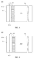
- FIG. 8 illustrates a top view of a light guide plate in accordance with a fifth embodiment of the present invention.
- FIG. 9 illustrates a bottom view of the light guide plate in accordance with the fifth embodiment of the present invention.
- FIG. 10 illustrates a side view of a light guide plate in accordance with a sixth embodiment of the present invention.
- FIG. 11 illustrates a side view of a light guide plate in accordance with a seventh embodiment of the present invention.
- FIG. 12 illustrates a side view of a light guide plate in accordance with an eighth embodiment of the present invention.
- FIG. 13 illustrates a perspective view of a display device in accordance with an embodiment of the present invention.
- FIG. 1 illustrates a perspective view of a backlight module 400 in accordance with an embodiment of the present invention.
- the backlight module 400 of the present embodiment mainly includes a light guide plate 500 and a light source 410 .
- the light source 410 is disposed at a side of the light guide plate 500 .
- the light guide plate 500 mainly includes a main body 510 , plural first strip structures 520 and plural second strip structures 530 .
- the first strip structures 520 and the second strip structures 530 are disposed on the main body 510 .
- the first strip structures 520 and the second strip structures 530 are used to mix light leaked from a portion near the light-incident side of the light guide plate 500 , thereby reducing a non-uniform brightness phenomenon generated adjacent to the light-incident side of the light guide plate 500 and increasing illumination uniformity of the backlight module 400 .
- the main body 510 of the light guide plate 500 mainly includes a light incident surface 511 , an end portion 512 , a light guide portion 513 and a side surface 514 .
- the end portion 512 is a tapered structure and has one end with greater thickness and the other end with smaller thickness.
- the light incident surface 511 is located at the end of the end portion 512 which has greater thickness.
- the light guide portion 513 is connected to the end of the end portion 512 which has smaller thickness.
- the light guide portion 513 is a flat plate with a uniform thickness.
- the end portion 512 has a first inclined surface 512 a and a second inclined surface 512 b respectively connected to two opposite sides of the light incident surface 511 .
- the light guide portion 513 has a first optical surface 513 a and a second optical surface 513 b opposite to each other.
- the side surface 514 is located at a side of the light guide portion 513 away from the end portion 512 , and the side surface 514 is connected to the first optical surface 513 a and the second optical surface 513 b .
- the first inclined surface 512 a has a first top edge 512 c and a first bottom edge 512 d
- the second inclined surface 512 b has a second top edge 512 e and a second bottom edge 512 f .
- the light incident surface 511 is connected to the first top edge 512 c and the second top edge 512 e
- the first optical surface 513 a is connected to the first bottom edge 512 d of the first inclined surface 512 a
- the second optical surface 513 b is connected to second bottom edge 512 f of the second inclined surface 512 b.
- FIG. 2 and FIG. 3 illustrate a top view and a bottom view of the light guide plate 500 in accordance with a first embodiment of the present invention.
- An extending direction of each of the first strip structures 520 and the second strip structures 530 is vertical to the light incident surface 511 .
- at least one portion of each first strip structure 520 is disposed on the first optical surface 513 a
- at least one portion of each second strip structure 530 is disposed on the second optical surface 513 b .
- each first strip structure 520 is connected to the first bottom edge 512 d of the first inclined surface 512 a , and the other end of each first strip structure 520 is located between the incidence surface 511 and the side surface 514 .
- One end of each second strip structure 530 is connected to the second bottom edge 512 f of the second inclined surface 512 b , and the other end of each second strip structure 530 is located between the incidence surface 511 and the side surface 514 .
- each of the first strip structures 520 and the second strip structures 530 extends along a direction away from the light incident surface 511 of the main body 510 .
- each of the first strip structures 520 and the second strip structures 530 is vertical to the light incident surface 511 of the main body 510 (as shown in the present embodiment), or each of the first strip structures 520 and the second strip structures 530 can be inclined relative to the light incident surface 511 of the main body 510 (as shown in FIG. 10 ).
- the backlight module 400 further includes a reflecting film 420 disposed at a side of the second optical surface 513 b of the light guide plate 500 .
- the reflecting film 420 is used to reflect light which emitted from the second inclined surface 512 b or second optical surface 513 b back to the light guide plate 500 .
- first strip structures 520 and second strip structures 530 are disposed on the main body 510 , so as to solve the problem of the bright bands or non-uniform brightness on the light guide plate 500 .
- a propagation path of light directly emitted from the first inclined surface 512 a or the first optical surface 513 a is different from a propagation path of light emitted from the second inclined surface 512 b or the second optical surface 513 b , reflected back to the main body 510 by the reflecting film 420 , and then emitted from the first inclined surface 512 a or the first optical surface 513 a . Therefore, an inherent type, an arrangement manner or an arrangement position of the first strip structures 520 is different from an inherent type, an arrangement manner or an arrangement position of the second strip structures 530 . It is noted that, the “inherent type” used herein means lengths, heights, depths or widths of the first strip structures 520 and the second strip structures 530 .
- a feature of each of the second strip structures 530 is more significant than a feature of each of the first strip structures 520 .
- a length L 2 of each of the second strip structures 530 is greater than a length L 1 of each of the first strip structures 520 .
- the first optical surface 513 a is a light-emitting surface of the backlight module 400 .
- the display panel 910 is disposed on the backlight module 400 .
- a black edge of the display panel 910 which is not used to display images can be defined as a non-display area, and a central region of the display panel 910 which can display images can be defined as an active area.
- the first strip structures 520 , the second strip structures 530 and the end portion 512 of the light guide plate 500 are disposed in the non-display area so as to avoid affecting the light-emitting quality of the active area.
- the non-display area itself as well as the first strip structures 520 and second strip structures 530 have to be designed to be very small, and therefore second strip structures 530 located on the second optical surface 513 b which have more significant feature can effectively improve light-emitting effect of the active area of the light guide plate 500 .
- FIG. 4 illustrates a side view of a light guide plate 610 in accordance with a second embodiment of the present invention.
- the structure of the light guide plate 610 in FIG. 4 is similar to that of the light guide plate 500 in FIG. 1 , and the main difference therebetween is that first strip structures 612 and second strip structures 614 of the light guide plate 610 have different heights.
- each of the first strip structures 612 and second strip structures 614 is a convex structure.
- Each of the first strip structures 612 has a height H 1
- each of the second strip structures 614 has a height H 2 .
- the height H 1 is different from the height H 2 .
- the height H 1 of each first strip structure 612 is smaller than the height H 2 of each second strip structure 614 .
- the feature of each second strip structure 614 is more significant than that of each first strip structure 612 . Therefore, when the first strip structures 612 and the second strip structures 614 are designed to be very small, the second strip structures 614 located on the second optical surface 513 b which have more significant feature can effectively improve light-emitting effect of an active area of the light guide plate 610 .
- a length of the first strip structures 612 is equal to a length of the second strip structures 614 . In other embodiments, the length of the first strip structures 612 can be designed to be different from the length of the second strip structures 614 according to different requirements.
- FIG. 5 illustrates a side view of a light guide plate 620 in accordance with a third embodiment of the present invention.
- the structure of the light guide plate 620 in FIG. 5 is similar to that of the light guide plate 610 in FIG. 4 , and the main difference therebetween is that each of first strip structures 622 and second strip structures 624 of the light guide plate 620 is a concave structure, and the first strip structures 622 and second strip structures 624 have different depths.
- each of the first strip structures 622 has a depth D 1 and each of the second strip structures 624 has a depth D 2 .
- the depth D 1 is different from the depth D 2 .
- each first strip structure 622 is smaller than the depth D 2 of each second strip structure 624 .
- the feature of each second strip structure 624 is more significant than that of each first strip structure 622 . Therefore, when the first strip structures 622 and the second strip structures 624 are designed to be very small, the second strip structures 624 located on the second optical surface 513 b which have more significant feature can effectively improve light-emitting effect of an active area of the light guide plate 620 .
- a length of the first strip structures 622 is equal to a length of the second strip structures 624 . In other embodiments, the length of the first strip structures 622 can be designed to be different from the length of the second strip structures 624 according to different requirements.
- the arrangement densities of the first strip structures and the second strip structures can be varied according to different requirements.
- FIG. 6 and FIG. 7 illustrate a top view and a bottom view of a light guide plate 630 in accordance with a fourth embodiment of the present invention.
- the structure of the light guide plate 630 in FIG. 6 and FIG. 7 is similar to that of the light guide plate 500 in FIG. 1 , and the main difference therebetween is that an arrangement distance between each first strip structure 632 is different from an arrangement distance between each second strip structure 634 .
- FIG. 6 there is a first distance W 1 between any two adjacent first strip structures 632 .
- the first distance W 1 is different from the second distance W 2 .
- the second distance W 2 is smaller than the first distance W 1 .
- the second strip structures 634 are arranged more densely than the first strip structures 632 . Therefore, the second strip structures 634 located on a back surface of the light guide plate 630 (i.e. the second optical surface 513 b which is not used as a light-emitting surface) which have greater arrangement density can effectively improve light-emitting effect of an active area of the light guide plate 630 .
- a length of the first strip structures 632 is equal to a length of the second strip structures 634 .
- the length of the first strip structures 632 can be designed to be different from the length of the second strip structures 634 according to different requirements.
- a height (or depth) of each first strip structure 632 and a height (or depth) of each second strip structure 634 can be designed to be equal or unequal according to different requirements.
- the first strip structures 520 , 612 , 622 and 632 of the light guide plate 500 , 610 , 620 and 630 which are connected to the first bottom edge 512 d of the first inclined surface 512 a , and the second strip structures 530 , 614 , 624 and 634 which are connected to the second bottom edge 512 f of the second inclined surface 512 b are merely used as an example for explanation, and embodiments of the present invention are not limited thereto.
- the first strip structures can be not connected to the first bottom edge 512 d
- the second strip structures can be not connected to the second bottom edge 512 f .
- the first strip structures can be spaced from the first bottom edge at a distance
- the second strip structures can be spaced from the second bottom edge at a distance.
- FIG. 8 and FIG. 9 illustrate a top view and a bottom view of a light guide plate 640 in accordance with a fifth embodiment of the present invention.
- the structure of the light guide plate 640 in FIG. 8 and FIG. 9 is similar to that of the light guide plate 500 in FIG. 1 , and the main difference therebetween is that a first distance L 3 between first strip structures 642 of the light guide plate 640 and the first bottom edge 512 d is different from a second distance L 4 between second strip structures 644 of the light guide plate 640 and the second bottom edge 512 f .
- the second distance L 4 is greater than the first distance L 3 .
- the second strip structures 644 located on a middle region of a back surface (i.e. the second optical surface 513 b which is not used as a light-emitting surface) of the light guide plate 640 can effectively improve light-emitting effect of the active area of the light guide plate 640 .
- an extending direction of a portion of each first strip structure 642 located on the first optical surface 513 a and an extending direction of a portion of each second strip structure 644 located on the second optical surface 513 b are parallel to a normal line vertical to the light incident surface 511 .
- lengths of the first strip structures 642 and the second strip structures 644 are smaller than a length of the main body 510 of the light guide plate 640 .
- the length of the first strip structures 642 is equal to the length of the second strip structures 644 .
- the length of the first strip structures 642 can be designed to be different from the length of the second strip structures 644 according to different requirements.
- a height (or depth) of each first strip structure 642 and a height (or depth) of each second strip structure 644 can be designed to be equal or unequal according to different requirements.
- each first strip structure 520 of FIG. 1 which is connected to the first bottom edge 512 d of the first inclined surface 512 a
- one end of each second strip structure 530 is connected to the second bottom edge 512 f of the second inclined surface 512 b
- the other end of each second strip structure 530 which is located between the light incident surface 511 and the side surface 514 are merely used as an example for explanation, and embodiments of the present invention are not limited thereto.
- FIG. 10 illustrates a side view of a light guide plate 650 in accordance with a sixth embodiment of the present invention.
- the structure of the light guide plate 650 in FIG. 10 is similar to that of the light guide plate 500 in FIG. 1 , and the main difference therebetween is that first strip structures 652 and second strip structures 654 of the light guide plate 650 have different designs.
- one end of the first strip structure 652 near the light incident surface 511 is located on the first inclined surface 512 a
- the other end of the first strip structure 652 away from the light incident surface 511 is located on the first optical surface 513 a between the light incident surface 511 and the side surface 514 .
- One end of the second strip structure 654 near the light incident surface 511 is located on the second inclined surface 512 b
- the other end of the second strip structure 654 away from the light incident surface 511 is located on the second optical surface 513 b between the light incident surface 511 and the side surface 514 .
- first strip structures 652 and second strip structures 654 are similar to those of the first strip structures 520 , 612 , 622 , 632 and 642 and the second strip structures 530 , 614 , 624 , 634 and 644 shown in FIG. 1 - FIG. 9 , and therefore will not be described again herein.
- FIG. 11 illustrates a side view of a light guide plate 700 in accordance with a seventh embodiment of the present invention.
- the light guide plate 700 of the present embodiment mainly includes a main body 710 , plural first strip structures 720 and plural second strip structures 730 .
- the main body 710 mainly includes a light incident surface 711 , an end portion 712 , a light guide portion 713 and a side surface 714 .
- the end portion 712 is a tapered structure and has one end with greater thickness and the other end with smaller thickness. As shown in FIG.
- the end portion 712 includes a first platform surface 712 a , a second platform surface 712 b , a first inclined surface 712 c and a second inclined surface 712 d .
- the light incident surface 711 is located at a the end of the end portion 712 which has greater thickness, and the light incident surface 711 is connected to the first platform surface 712 a and the second platform surface 712 b .
- the light guide portion 713 is connected to the end of the end portion 712 which has smaller thickness, and the light guide portion 713 is a flat plate with a uniform thickness.
- the light guide portion 713 includes a first optical surface 713 a and a second optical surface 713 b opposite to each other.
- the first inclined surface 712 c of the end portion 712 has a first top edge 712 e and a first bottom edge 712 f .
- the first top edge 712 e is connected to the first platform surface 712 a
- the first bottom edge 712 f is connected to the first optical surface 713 a .
- the second inclined surface 712 d has a second top edge 712 g and a second bottom edge 712 h .
- the second top edge 712 g is connected to the second platform surface 712 b
- the second bottom edge 712 h is connected to the second optical surface 713 b .
- first strip structures 720 and second strip structures 730 are similar to those of the first strip structures 520 , 612 , 622 , 632 , 642 and 652 and the second strip structures 530 , 614 , 624 , 634 , 644 and 654 shown in FIG. 1 - FIG. 10 , and therefore will not be described again herein.
- FIG. 12 illustrates a side view of a light guide plate 800 in accordance with an eighth embodiment of the present invention.
- the light guide plate 800 of the present embodiment mainly includes a main body 810 , plural first strip structures 820 and plural second strip structures 830 .
- the main body 810 mainly includes a light incident surface 811 , an end portion 812 and a light guide portion 813 .
- the end portion 812 is a tapered structure and has one end with greater thickness and the other end with smaller thickness.
- the end portion 812 has an inclined surface 812 a at one side and a flat surface 812 b at the other side. As shown in FIG.
- the light incident surface 811 is located on the end of the end portion 812 which has greater thickness
- the light guide portion 813 is connected to the end of the end portion 812 which has smaller thickness.
- the light guide portion 813 is a flat plate with a uniform thickness.
- the light guide portion 813 has a first optical surface 813 a and a second optical surface 813 b opposite to each other.
- the first strip structures 820 and the second strip structures 830 are respectively disposed on the first optical surface 813 a and the second optical surface 813 b . It is noted that, the designs, the arrangement manners and the effects of the first strip structures 820 and second strip structures 830 are similar to those of the first strip structures 520 , 612 , 622 , 632 , 642 , 652 and 720 and the second strip structures 530 , 614 , 624 , 634 , 644 , 654 and 730 shown in FIG. 1 - FIG. 11 , and therefore will not be described again herein.
- FIG. 13 illustrates a perspective view of a display device 900 in accordance with an embodiment of the present invention.
- the display device 900 of the present embodiment includes a backlight module 400 shown in FIG. 1 and a display panel 910 .
- the display panel 910 is disposed in front of the first optical surface 513 a of the light guide plate 500 in the backlight module 400 .
- the first strip structures 520 of the light guide plate 500 is disposed corresponding to the non-display area of the display panel, and the first strip structures 520 can be used to cooperate with the second strip structures 530 so as to achieve the objectives of adjusting light as described above and will not be described therein.
- the backlight module 400 having the light guide plate 500 shown in FIG. 1 is merely used as an example applied to the display device 800 for explanation, and embodiments of the present invention are not limited thereto.
- other backlight modules such as the backlight modules having the light guide plate 500 , 610 , 620 , 630 , 640 , 650 and 700 also can be applied to a display device, so as to achieve the same effect.
- the light guide plate has different first strip structures and second strip structures respectively disposed on first optical surface and the second optical surface. Therefore, the first strip structures can effectively mix light leaked from the first optical surface near the connection portion between the end portion and the light guide portion, and the second strip structures can effectively mix light leaked from the second optical surface near the connection portion between the end portion and the light guide portion, thereby solving the problems of bright band or non-uniform brightness.
Landscapes
- Physics & Mathematics (AREA)
- General Physics & Mathematics (AREA)
- Optics & Photonics (AREA)
- Planar Illumination Modules (AREA)
Abstract
Description
Claims (29)
Applications Claiming Priority (1)
| Application Number | Priority Date | Filing Date | Title |
|---|---|---|---|
| PCT/CN2016/100770 WO2018058423A1 (en) | 2016-09-29 | 2016-09-29 | Light guide plate, backlight module and display device |
Related Parent Applications (1)
| Application Number | Title | Priority Date | Filing Date |
|---|---|---|---|
| PCT/CN2016/100770 Continuation WO2018058423A1 (en) | 2016-09-29 | 2016-09-29 | Light guide plate, backlight module and display device |
Publications (2)
| Publication Number | Publication Date |
|---|---|
| US20180088267A1 US20180088267A1 (en) | 2018-03-29 |
| US10338292B2 true US10338292B2 (en) | 2019-07-02 |
Family
ID=61686103
Family Applications (1)
| Application Number | Title | Priority Date | Filing Date |
|---|---|---|---|
| US15/686,170 Active US10338292B2 (en) | 2016-09-29 | 2017-08-25 | Light guide plate, backlight module and display device |
Country Status (4)
| Country | Link |
|---|---|
| US (1) | US10338292B2 (en) |
| CN (1) | CN108139045B (en) |
| TW (1) | TWI631378B (en) |
| WO (1) | WO2018058423A1 (en) |
Families Citing this family (2)
| Publication number | Priority date | Publication date | Assignee | Title |
|---|---|---|---|---|
| CN111610590A (en) * | 2019-02-26 | 2020-09-01 | 瑞仪光电(南京)有限公司 | Light guide plate, backlight module and display device |
| CN114114520A (en) * | 2021-11-18 | 2022-03-01 | 友达光电(昆山)有限公司 | Light guide plate, optical assembly and display device |
Citations (14)
| Publication number | Priority date | Publication date | Assignee | Title |
|---|---|---|---|---|
| TWM350026U (en) | 2008-09-09 | 2009-02-01 | Nano Prec Corp | Light guide plate |
| TWM445701U (en) | 2012-06-27 | 2013-01-21 | Young Lighting Technology Inc | Backlight module and light guide plate |
| KR20130048351A (en) | 2011-11-02 | 2013-05-10 | 엘지디스플레이 주식회사 | Light guide plate and backlight unit |
| CN103257391A (en) | 2013-01-08 | 2013-08-21 | 友达光电股份有限公司 | Light guide plate and backlight module |
| CN103307512A (en) | 2012-03-15 | 2013-09-18 | 欧姆龙株式会社 | Surface light source device and liquid crystal display device |
| US8625050B2 (en) | 2007-06-12 | 2014-01-07 | Omron Corporation | Surface light source apparatus |
| CN103901528A (en) | 2012-12-26 | 2014-07-02 | 欧姆龙株式会社 | Surface light source device and its light guide plate |
| US20140211125A1 (en) * | 2013-01-30 | 2014-07-31 | Omron Corporation | Light guide plate and surface illumination device |
| TWI457622B (en) | 2012-03-16 | 2014-10-21 | Radiant Opto Electronics Corp | Light guide plate and backlight module |
| CN203909333U (en) | 2014-07-02 | 2014-10-29 | 沈阳达源光电子有限公司 | Mobile phone backlight plate with novel light guide plate structure |
| US20150092440A1 (en) | 2013-09-30 | 2015-04-02 | Samsung Display Co., Ltd. | Light guide panel, back light assembly and diplay apparatus each having the light guide panel and method of manufacturing the light guide panel |
| TWI485450B (en) | 2012-12-27 | 2015-05-21 | Au Optronics Corp | Light guide plate and backlight module |
| CN205246927U (en) | 2015-11-20 | 2016-05-18 | 瑞仪光电股份有限公司 | Display device |
| CN205402403U (en) | 2016-03-07 | 2016-07-27 | 瑞仪光电(苏州)有限公司 | Backlight module and display device |
Family Cites Families (11)
| Publication number | Priority date | Publication date | Assignee | Title |
|---|---|---|---|---|
| JP3280828B2 (en) * | 1995-06-30 | 2002-05-13 | 富士通化成株式会社 | Backlight unit |
| US6464365B1 (en) * | 1999-07-23 | 2002-10-15 | Bae Systems Information And Electronic Systems Integration Inc. | Light collimator for liquid crystal displays |
| JP5088417B2 (en) * | 2008-12-16 | 2012-12-05 | オムロン株式会社 | Surface light source device |
| US8931943B2 (en) * | 2011-12-22 | 2015-01-13 | Minebea Co., Ltd. | Spread illuminating apparatus |
| JP5532109B2 (en) * | 2012-11-15 | 2014-06-25 | オムロン株式会社 | Light guide plate and surface light source device |
| JP5862557B2 (en) * | 2012-12-26 | 2016-02-16 | オムロン株式会社 | Light guide plate and surface light source device |
| JP2014130748A (en) * | 2012-12-28 | 2014-07-10 | Omron Corp | Light guide plate and surface light source device |
| CN103454716A (en) * | 2013-08-27 | 2013-12-18 | 北京京东方光电科技有限公司 | Light guide plate, manufacturing method thereof, backlight module and display device |
| JP6288442B2 (en) * | 2014-04-09 | 2018-03-07 | オムロン株式会社 | Light guide plate and surface light source device |
| CN104714271A (en) * | 2015-03-30 | 2015-06-17 | 深圳市华星光电技术有限公司 | Light guide plate and backlight module |
| CN206479662U (en) * | 2016-09-29 | 2017-09-08 | 瑞仪光电股份有限公司 | Display device |
-
2016
- 2016-09-29 WO PCT/CN2016/100770 patent/WO2018058423A1/en not_active Ceased
- 2016-09-29 CN CN201680016214.5A patent/CN108139045B/en active Active
- 2016-10-28 TW TW105135089A patent/TWI631378B/en not_active IP Right Cessation
-
2017
- 2017-08-25 US US15/686,170 patent/US10338292B2/en active Active
Patent Citations (14)
| Publication number | Priority date | Publication date | Assignee | Title |
|---|---|---|---|---|
| US8625050B2 (en) | 2007-06-12 | 2014-01-07 | Omron Corporation | Surface light source apparatus |
| TWM350026U (en) | 2008-09-09 | 2009-02-01 | Nano Prec Corp | Light guide plate |
| KR20130048351A (en) | 2011-11-02 | 2013-05-10 | 엘지디스플레이 주식회사 | Light guide plate and backlight unit |
| CN103307512A (en) | 2012-03-15 | 2013-09-18 | 欧姆龙株式会社 | Surface light source device and liquid crystal display device |
| TWI457622B (en) | 2012-03-16 | 2014-10-21 | Radiant Opto Electronics Corp | Light guide plate and backlight module |
| TWM445701U (en) | 2012-06-27 | 2013-01-21 | Young Lighting Technology Inc | Backlight module and light guide plate |
| CN103901528A (en) | 2012-12-26 | 2014-07-02 | 欧姆龙株式会社 | Surface light source device and its light guide plate |
| TWI485450B (en) | 2012-12-27 | 2015-05-21 | Au Optronics Corp | Light guide plate and backlight module |
| CN103257391A (en) | 2013-01-08 | 2013-08-21 | 友达光电股份有限公司 | Light guide plate and backlight module |
| US20140211125A1 (en) * | 2013-01-30 | 2014-07-31 | Omron Corporation | Light guide plate and surface illumination device |
| US20150092440A1 (en) | 2013-09-30 | 2015-04-02 | Samsung Display Co., Ltd. | Light guide panel, back light assembly and diplay apparatus each having the light guide panel and method of manufacturing the light guide panel |
| CN203909333U (en) | 2014-07-02 | 2014-10-29 | 沈阳达源光电子有限公司 | Mobile phone backlight plate with novel light guide plate structure |
| CN205246927U (en) | 2015-11-20 | 2016-05-18 | 瑞仪光电股份有限公司 | Display device |
| CN205402403U (en) | 2016-03-07 | 2016-07-27 | 瑞仪光电(苏州)有限公司 | Backlight module and display device |
Also Published As
| Publication number | Publication date |
|---|---|
| WO2018058423A1 (en) | 2018-04-05 |
| TW201814343A (en) | 2018-04-16 |
| CN108139045B (en) | 2020-10-20 |
| US20180088267A1 (en) | 2018-03-29 |
| CN108139045A (en) | 2018-06-08 |
| TWI631378B (en) | 2018-08-01 |
Similar Documents
| Publication | Publication Date | Title |
|---|---|---|
| US8684588B2 (en) | Light guide elements for display device | |
| US20100134722A1 (en) | Backlight module and display device using the same | |
| TW201416776A (en) | Planar light source device, liquid crystal display device and mobile device | |
| TW201040630A (en) | Backlight unit | |
| US10386565B2 (en) | Surface light source assembly having light guide with groove structures for out-coupling light, and backlight module having the surface light source assembly | |
| CN104977647B (en) | Light guide plate and planar light source device | |
| US9535204B2 (en) | Illumination apparatus having light guide plate with curvedly tapered light coupling portion | |
| JP2018190708A (en) | Backlight module and surface light source assembly thereof | |
| JP2017120740A (en) | Light guide plate, surface light source device, display device, and electronic apparatus | |
| US20110019435A1 (en) | Brightness enhancement film and backlight module | |
| CN206479662U (en) | Display device | |
| US8405796B2 (en) | Illumination device, surface light source device, and liquid crystal display device | |
| KR20010030296A (en) | Surface light source device and image display device with the same device | |
| US10338292B2 (en) | Light guide plate, backlight module and display device | |
| US10185071B2 (en) | Light guide plate, backlight module and display device | |
| CN101285963A (en) | Backlight module | |
| US10816715B2 (en) | Light guide plate, backlight module and display device | |
| US9891366B2 (en) | Backlight module | |
| US20100277949A1 (en) | Light guide plate and backlight module | |
| JP4584116B2 (en) | Point source backlight | |
| JP2010287556A (en) | Lighting device and display including the same | |
| JP6682834B2 (en) | Light guide plate, surface light source device, display device, and electronic device | |
| CN210270457U (en) | Backlight module, display module and display device | |
| US10976594B2 (en) | Light guide plate, light source assembly, display panel and display device | |
| JP2022023207A (en) | Display device |
Legal Events
| Date | Code | Title | Description |
|---|---|---|---|
| AS | Assignment |
Owner name: RADIANT OPTO-ELECTRONICS (SUZHOU) CO.,LTD., CHINA Free format text: ASSIGNMENT OF ASSIGNORS INTEREST;ASSIGNORS:CHANG, CHIA-YIN;LIN, SHIN-BO;REEL/FRAME:043414/0767 Effective date: 20160721 Owner name: RADIANT OPTO-ELECTRONICS CORPORATION, TAIWAN Free format text: ASSIGNMENT OF ASSIGNORS INTEREST;ASSIGNORS:CHANG, CHIA-YIN;LIN, SHIN-BO;REEL/FRAME:043414/0767 Effective date: 20160721 |
|
| STPP | Information on status: patent application and granting procedure in general |
Free format text: RESPONSE TO NON-FINAL OFFICE ACTION ENTERED AND FORWARDED TO EXAMINER |
|
| STPP | Information on status: patent application and granting procedure in general |
Free format text: NOTICE OF ALLOWANCE MAILED -- APPLICATION RECEIVED IN OFFICE OF PUBLICATIONS |
|
| STPP | Information on status: patent application and granting procedure in general |
Free format text: PUBLICATIONS -- ISSUE FEE PAYMENT VERIFIED |
|
| STCF | Information on status: patent grant |
Free format text: PATENTED CASE |
|
| MAFP | Maintenance fee payment |
Free format text: PAYMENT OF MAINTENANCE FEE, 4TH YEAR, LARGE ENTITY (ORIGINAL EVENT CODE: M1551); ENTITY STATUS OF PATENT OWNER: LARGE ENTITY Year of fee payment: 4 |