US10320430B2 - Transmitter with power supply rejection - Google Patents
Transmitter with power supply rejection Download PDFInfo
- Publication number
- US10320430B2 US10320430B2 US15/721,535 US201715721535A US10320430B2 US 10320430 B2 US10320430 B2 US 10320430B2 US 201715721535 A US201715721535 A US 201715721535A US 10320430 B2 US10320430 B2 US 10320430B2
- Authority
- US
- United States
- Prior art keywords
- driver
- circuitry
- output
- power supply
- code
- Prior art date
- Legal status (The legal status is an assumption and is not a legal conclusion. Google has not performed a legal analysis and makes no representation as to the accuracy of the status listed.)
- Expired - Fee Related
Links
Images


Classifications
-
- H—ELECTRICITY
- H04—ELECTRIC COMMUNICATION TECHNIQUE
- H04B—TRANSMISSION
- H04B1/00—Details of transmission systems, not covered by a single one of groups H04B3/00 - H04B13/00; Details of transmission systems not characterised by the medium used for transmission
- H04B1/02—Transmitters
- H04B1/04—Circuits
-
- G—PHYSICS
- G06—COMPUTING OR CALCULATING; COUNTING
- G06F—ELECTRIC DIGITAL DATA PROCESSING
- G06F1/00—Details not covered by groups G06F3/00 - G06F13/00 and G06F21/00
- G06F1/26—Power supply means, e.g. regulation thereof
- G06F1/30—Means for acting in the event of power-supply failure or interruption, e.g. power-supply fluctuations
- G06F1/305—Means for acting in the event of power-supply failure or interruption, e.g. power-supply fluctuations in the event of power-supply fluctuations
-
- G—PHYSICS
- G06—COMPUTING OR CALCULATING; COUNTING
- G06F—ELECTRIC DIGITAL DATA PROCESSING
- G06F13/00—Interconnection of, or transfer of information or other signals between, memories, input/output devices or central processing units
- G06F13/38—Information transfer, e.g. on bus
- G06F13/40—Bus structure
- G06F13/4063—Device-to-bus coupling
- G06F13/4068—Electrical coupling
- G06F13/4072—Drivers or receivers
-
- H—ELECTRICITY
- H04—ELECTRIC COMMUNICATION TECHNIQUE
- H04B—TRANSMISSION
- H04B1/00—Details of transmission systems, not covered by a single one of groups H04B3/00 - H04B13/00; Details of transmission systems not characterised by the medium used for transmission
- H04B1/06—Receivers
- H04B1/16—Circuits
- H04B1/1607—Supply circuits
Definitions
- FIG. 1 illustrates a system showing a push-pull driver and receiver.
- FIG. 2 illustrates a plot showing an eye diagram at the connector of the system.
- FIG. 3 illustrates an apparatus for adjusting voltage swing of a push-pull driver according to noise on a power supply, according to some embodiments of the disclosure.
- FIG. 4 illustrates a schematic view of the apparatus of FIG. 3 , according to some embodiments of the disclosure.
- FIG. 5 illustrates a calibration logic of the apparatus of FIG. 3 , according to some embodiments of the disclosure.
- FIG. 6 illustrates a schematic view of the push-pull driver with adjustable voltage swing, according to some embodiments of the disclosure.
- FIG. 7 illustrates a timing diagram of the calibration logic of the apparatus of FIG. 3 , according to some embodiments of the disclosure.
- FIG. 8 illustrates a flowchart of a method of calibrating the push-pull driver, according to some embodiments of the disclosure.
- FIG. 9 illustrates a smart device or a computer system or a System-on-Chip (SoC) with the push-pull driver having adjustable voltage swing, according to some embodiments.
- SoC System-on-Chip
- a sense circuitry is used to sense power supply noise or variation.
- a filtered power supply is used to power a ring oscillator, the frequency of which represents the sensed power supply noise.
- the frequency of an output clock from the ring oscillator also varies.
- the clock from the oscillator is compared with a reference clean clock, and a determination is made about whether the clock is faster or slower than the reference clock.
- a digital code is generated which is used to adjust a performance parameter of the driver output.
- a performance parameter is voltage swing at the output of the driver.
- a lookup table (LUT) is used to provide a target reference code across process variation. LUT is useful in deciding whether the process band design is on typical, fast or slow.
- the apparatus of various embodiments is mostly a digital solution, which is less sensitive towards supply variation and easily scalable to newer process technology nodes.
- the voltage swing of the driver output is adjusted by adjusting a reference current to a desired value without impacting transmitter output termination impedance.
- the apparatus of various embodiments is a generic design that can be used for other high speed transmitters and other power supply sensitive circuits.
- the digital code generated by a calibration circuitry can be used to adjust parameters other than voltage swing.
- signals are represented with lines. Some lines may be thicker, to indicate more constituent signal paths, and/or have arrows at one or more ends, to indicate primary information flow direction. Such indications are not intended to be limiting. Rather, the lines are used in connection with one or more exemplary embodiments to facilitate easier understanding of a circuit or a logical unit. Any represented signal, as dictated by design needs or preferences, may actually comprise one or more signals that may travel in either direction and may be implemented with any suitable type of signal scheme.
- connection means a direct connection, such as electrical, mechanical, or magnetic connection between the things that are connected, without any intermediary devices.
- coupled means a direct or indirect connection, such as a direct electrical, mechanical, or magnetic connection between the things that are connected or an indirect connection, through one or more passive or active intermediary devices.
- circuit or “module” may refer to one or more passive and/or active components that are arranged to cooperate with one another to provide a desired function.
- signal may refer to at least one current signal, voltage signal, magnetic signal, or data/clock signal.
- the meaning of “a,” “an,” and “the” include plural references.
- the meaning of “in” includes “in” and “on.”
- scaling generally refers to converting a design (schematic and layout) from one process technology to another process technology and subsequently being reduced in layout area.
- scaling generally also refers to downsizing layout and devices within the same technology node.
- scaling may also refer to adjusting (e.g., slowing down or speeding up—i.e. scaling down, or scaling up respectively) of a signal frequency relative to another parameter, for example, power supply level.
- scaling may also refer to adjusting the magnitude of the power supply voltage (e.g., voltage scaling) to the circuit(s).
- phrases “A and/or B” and “A or B” mean (A), (B), or (A and B).
- phrase “A, B, and/or C” means (A), (B), (C), (A and B), (A and C), (B and C), or (A, B and C).
- the terms “left,” “right,” “front,” “back,” “top,” “bottom,” “over,” “under,” and the like in the description and in the claims, if any, are used for descriptive purposes and not necessarily for describing permanent relative positions.
- the transistors in various circuits, modules, and logic blocks may be Tunneling FETs (TFETs) or some transistors of various embodiments may comprise metal oxide semiconductor (MOS) transistors, which include drain, source, gate, and bulk terminals.
- the transistors may also include Tri-Gate and FinFET transistors, Gate All Around Cylindrical Transistors, Square Wire, or Rectangular Ribbon Transistors or other devices implementing transistor functionality like carbon nano tubes or spintronic devices.
- MOSFET symmetrical source and drain terminals i.e., are identical terminals and are interchangeably used here.
- a TFET device on the other hand, has asymmetric Source and Drain terminals.
- Bi-polar junction transistors—BJT PNP/NPN, BiCMOS, CMOS, etc. may be used for some transistors without departing from the scope of the disclosure.
- FIG. 1 illustrates system 100 showing a push-pull driver and receiver.
- System 100 comprises a plurality of push-pull drivers 101 1-n , where ‘n’ is an integer.
- Push-pull drivers e.g., 101 1
- Push-pull drivers consist of a p-type pull-up device MPd coupled in series with an n-type pull-down device MNd.
- Input data DataIn (or DIN) is received at the gates of the p-type pull-up device MPd and n-type pull-down device MNd.
- the push-pull drivers operate on a first power supply (e.g., VCC1p0 indicating a 1.0 V power supply).
- the output of the push-pull driver is coupled to a pass-transistor Mdac in series with a resistor R.
- Mdac may operate on a higher power supply (e.g., VCC1p8 indicating a 1.8 V power supply) to control how many devices of Mdac need to be turned on.
- One push-pull driver may generate a first output DP and another push-pull driver may generate another output DP, and as such a differential output can be achieved.
- These outputs are received by a receiver 103 (modeled here as a pull-down termination R T ) via transmission lines 102 .
- Vsw VDD*R T /( R T +R PU ) (1)
- VDD the power supply (e.g., VCC1p0)
- R T the receiver termination
- R PU the pull-up impedance
- the pull-up impedance R PU and pull-down impedance R PD are calibrated by an impedance compensation (RCOMP) circuitry (not shown).
- RCOMP impedance compensation
- the reference voltages used for such calibration are also derived from the very power supply that suffers from supply variation. Using bandgap references for such calibration would increase the power and area cost of the overall driver architecture.
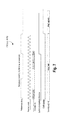
- FIG. 2 illustrates plot 200 showing an eye diagram at the connector of the system.
- the x-axis is time (ns) and the y-axis is voltage (V).
- the eye is shown by indicator 201 , while levels 202 and 203 illustrate the high and low limits of the voltage swing.
- Plot 200 shows an eye diagram formed across multiple process corner nodes. Due to power supply variation, the voltage swing varies and may use up more of the area of eye 201 , which may result in timing and other specification failures.
- the small eye opening of eye 201 means that additional circuitry along the pull-up and pull-down impedance paths may further reduce head-room which in turn will reduce eye height and width.
- One way to improve eye height and width is to use pre-emphasis circuitry. However, pre-emphasis circuitry adds power (e.g., 4 to 8 mW) to the driver architecture.
- FIG. 3 illustrates apparatus 300 for adjusting voltage swing of a push-pull driver according to noise (DC or AC) on a power supply, according to some embodiments of the disclosure.
- apparatus 300 comprises low pass filter (LPF) 301 , supply sensing block or circuitry 302 , calibration logic or circuitry 303 , and high-speed driver (pull-up/pull-down leg) 304 .
- LPF low pass filter
- LPF 301 is coupled to a first power supply (e.g., VCC_1p0 which refers to a 1.0 V power supply) and is used to detect DC (direct current) variation in the first power supply.
- the output of LPF 301 is VCC_Sense, which is a filtered version of the first power supply.
- the cut-off frequency of the LPF is less than 10 MHz, and can be fixed or programmed.
- LPF 301 is removed so as to sense AC (alternating current) variation in the first power supply.
- the first power supply is directly coupled to the Supply Sensing Block 302 .
- Supply Sensing block 302 senses the filtered (or in one case, unfiltered) VCC_Sense and converts the voltage of that supply into a digital domain. For example, a clock (Sense_out) is generated whose frequency change represents change in VCC_Sense. As such, noise or variation on VCC_Sense is captured as change in clock frequency.
- Supply Sensing block 302 comprises a ring oscillator which includes delay stages that substantially mimic the push-pull driver architecture of driver 304 . For example, most of the driver architecture minus the current mirror circuitry, discussed later with reference to FIG. 4 , is used as a delay stage of the ring oscillator. Referring back to FIG.
- the output of the Supply Sensing block 302 is Sense_out which is compared with a reference clock (Ref_Clock) in Calibration Logic 303 .
- Ref_Clock is a clean clock that can be provided by a crystal oscillator.
- Calibration Logic 303 is to adjust a reference digital code according to a LUT and a compensation code.
- the compensation code is an impedance compensation code which is used to adjust impedance (pull-up and/or pull-down) of driver 304 .
- the impedance compensation code may be generated by an impedance compensation circuitry (also referred to as RCOMP) that adjusts an impedance of a replica driver against a reference or target impedance, and once this impedance of the replica driver is adjusted for process, temperature, and voltage (PVT) variations, it is provided as an impedance compensation code to driver 304 and also stored in a LUT.
- RCOMP impedance compensation circuitry
- Calibration Logic 303 generates a time domain ratio, N Sensor , of the frequency of Sense_out (F Sense ) and Ref_Clock (F reference ).
- This time domain ratio N Sensor represents the variation of supply VCC_Sense against a reference.
- F Sense ( V ) 1/6*(0.69*( Reff*Cg ) where Reff is the effective pull-up or pull-down impedance of the replica driver used in a ring oscillator topology in Supply Sense Block 302 , and can be expressed R CPR +R Tran +R transmitter , and where Cg is an input capacitance of the replica driver.
- R CPR is the pull-up or pull-down resistance of the push-pull replica driver
- R Tran is the resistance of the pass-gate coupled to the output of the pull-up and pull-down devices of the driver
- R transmitter is the resistance of a resistor coupled in series with the pass-gate.
- Calibration Logic 303 generates a digital code N REF which is compared with N SENOR . In some embodiments, based on the comparison, Calibration Logic 303 determines whether calibration of the driver is needed. For example, when N SENSOR is above N REF by a particular amount (e.g., predetermined or programmable), Calibration Logic 303 determines that Calibration is needed, and CalibEN is enabled. In some embodiments, this particular amount is according to a frequency band, and is stored in a LUT.
- a particular amount e.g., predetermined or programmable
- Calibration Logic 303 when calibration is needed, Calibration Logic 303 generates a CalibUpdate signal and a digital code VswAdjust (e.g., 5 bits, [4:0]) to adjust a reference current of a current source of driver 304 .
- VswAdjust e.g., 5 bits, [4:0]
- an output voltage swing of the signal generated by driver 304 is adjusted to a desired or target level.
- the adjustment of the reference current does not change the termination impedance of driver 304 .
- a finite state machine is used to control the operation of Calibration Logic 303 .
- the FSM operates after an FSM of the RCOMP circuitry generates an impedance compensation code.
- driver 304 is an enhanced version of driver 101 .
- driver 304 includes a push-pull circuitry with transistors MPd and MNd, and Mdac.
- a current mirror network is added to the output of driver 304 to increase or decrease the signal strength driven by driver 304 without impacting its termination impedance.
- strength of a reference current source of the current mirror is adjusted by the digital code VswAdjust from Calibration Logic 303 , and is applied to the current source when CalibUpdate is enabled or asserted.
- the current mirror network operates on a higher power supply than the push-pull circuitry of driver 304 .
- the current mirror network operates at 1.8 V power supply.
- the current mirror network works at lower supply, for example, 1.0 V power supply.
- FIG. 4 illustrates a schematic view 400 of the apparatus of FIG. 3 , according to some embodiments of the disclosure. It is pointed out that those elements of FIG. 4 having the same reference numbers (or names) as the elements of any other figure can operate or function in any manner similar to that described, but are not limited to such.
- Supply Sense Block 302 comprises delay stages (e.g., 402 a , 402 b , 402 c ) configured to form a ring oscillator.
- each delay stage is a replica of driver 404 a .
- delay stage 402 a comprises a pull-up transistor having impedance Reffp, pull-down transistor having impedance Reffn, transmission gate transistor having impedance Rtran, and series termination resistor (or package resistor) R coupled together as shown.
- VCC_Sense is coupled to Vcc1p0 node of the delay stages 402 a - c .
- Vcc1p8 node is coupled to a fixed supply level of 1.8V.
- node names and signal names are interchangeably used.
- Vcc1p8 may refer to node Vcc1p8 or power supply Vcc1p8 on that node.
- the output clock Clock_out has a frequency which is a function of supply and process.
- the architecture of the delay stage is such that it has low sensitivity towards temperature.
- the ring oscillator of Supply Sense Block 302 is gated by CalibEn signal. For example, when calibration is enabled (e.g., when CalibEn is high), Supply Sense Block 302 is activated which allows for sensing of VCC_Sense in the form of oscillating clock Clock_out. Likewise, when calibration is disabled (e.g., when CalibEn is low), then Supply Block 302 is deactivated and Clock_out no longer oscillates.
- While the embodiments illustrate a ring oscillator with three delay stages 402 a , 402 b , and 402 c , other number of stages may be used. For example, three or five delay stages may be used and coupled together in a ring formation.
- Calibration logic 303 comprises comparator 403 a , filter 403 b , decision making logic 403 c , and LUT 403 d .
- comparator 403 a comprises a first input that receives Clock_out and a second input that receives Ref_Clock.
- comparator 403 a is a clocked comparator.
- the output of Comparator 403 a is filtered by filter 403 b .
- the output of Comparator 403 a is a ratio of Clock_out relative to Ref_Clock. By comparing Clock_out with an ideal or near ideal Ref_Clock, change in supply VCC_1p0 is determined.
- filter 403 a is a digital filter.
- filter 403 a is a chain of shift registers.
- filter 403 a is an analog filter.
- the output of filter 403 b is processed by Decision Making logic 403 c .
- the outputs of Decision Making logic 403 c include Calibration Enable signal (CalibEN), calibration update signal (CalibUpdate), and voltage swing adjustment code (VswAdjust).
- Decision Making logic 403 c is implemented as a finite state machine (FSM). In some embodiments, the FSM works in combination with an impedance control state machine as described with reference to FIG. 5 .
- driver 304 comprises a plurality of push-pull circuitries. So as not to obscure the embodiments, architecture of one push-pull circuitry 404 a is described. In some embodiments, push-pull circuitry 404 a is like 101 1 . In some embodiments, push-pull circuitry 404 a includes pull-up p-type transistor MPd, pull-down n-type transistor MNd, programmable transmission device Mdac (e.g., n-type device controlled by 5 bit digital to analog control bits), package or driver series impedance R (e.g., 45 Ohms), and current mirror circuitry 404 b .
- MPd pull-up p-type transistor MPd
- pull-down n-type transistor MNd programmable transmission device Mdac
- programmable transmission device Mdac e.g., n-type device controlled by 5 bit digital to analog control bits
- package or driver series impedance R e.g. 45 Ohms
- each push-pull circuitry has a corresponding current mirror circuitry 404 b .
- multiple push-pull circuitries share the same current mirror circuitry 404 b .
- ‘n’ number of push-pull circuitries that are adjacent to one another can share the same current mirror circuitry 404 b.
- current mirror circuitry 404 b comprises a first reference current source Is1, a second reference current source Is2, and a current mirror device MPcm coupled together as shown.
- the first reference current source Is1 mirrors the current Is2 by a factor (e.g., a factor of 1 or more).
- the first reference current source Is1 is a p-type transistor with its gate terminal coupled to the gate terminal of transistor MPcm, source terminal coupled to Vcc1p8, and drain terminal coupled to the output node DP/DM.
- the embodiments are not limited to this particular current mirror circuitry, and other such circuitries that can have variable current strength using a digital code can also be used.
- Is2 is adjusted to adjust output swing on nodes DP/DM. As such, transmitter impedance change is not changed.
- Calibration Logic 303 compares Clock_out with Ref Clock to generate a reference code based on a predetermined or stored target reference count in LUT 403 d .
- LUT 403 d may have different count values for different frequency bands.
- a particular count value is assigned. This count value is then used to generate the code which is filtered by filter 403 b , in accordance with some embodiments.
- Decision making logic 403 c uses the output of filter 403 b to generate VswAdjust code for adjusting the reference current Is2 of driver 304 . By digitally adjusting reference current Is2, the voltage swing of signal on node DP/DM is adjusted.
- the embodiments are not limited to such.
- the scheme of various embodiments is also applicable to cases where both push-up and pull-down devices are n-type only or p-type only. In those cases, the replica branches are to have similar architecture.
- FIG. 5 illustrates calibration logic 500 (e.g., 303 ) of the apparatus of FIG. 3 , according to some embodiments of the disclosure. It is pointed out that those elements of FIG. 5 having the same reference numbers (or names) as the elements of any other figure can operate or function in any manner similar to that described, but are not limited to such.
- FIG. 5 illustrates a functional schematic of calibration logic 500 which includes counter 501 , register 502 that saves the count value, sequential 503 , logic 504 to compare the count value with a reference count, and combinational logic 505 .
- counter 501 counts the number of pulses in Clock_out within a Ref_Clock and stores that in register 502 .
- the signal Upload is used for latching the final counter value during lock time to compare.
- the final counter value is latched.
- Sampled clock is the sampling clock which is used to sample the counter value. This is a low frequency clock and is used to latch the final value after a sampling window. This sampled value is used for comparison purposes.
- the output of register 502 is sampled and the Count is compared with a reference count (Ref count).
- the Ref (reference) count is a fixed code provided by Vref (e.g., 8 bit count code).
- Vref is fixed digital code which acts as a reference voltage in the digital domain.
- Vref is less susceptible to noise as compared to a traditional analog signal.
- This reference code is a fixed and programmable code based on what value is needed to be programmed.
- an analog signal is any continuous signal for which the time varying feature (variable) of the signal is a representation of some other time varying quantity, i.e., analogous to another time varying signal, while a digital signal is a physical signal that is a representation of a sequence of discrete values (a quantified discrete-time signal), for example of an arbitrary bit stream, or of a digitized (sampled and analog-to-digital converted) analog signal.
- FIG. 6 illustrates schematic view 600 (e.g., 304 ) of the push-pull driver with adjustable voltage swing, according to some embodiments of the disclosure. It is pointed out that those elements of FIG. 6 having the same reference numbers (or names) as the elements of any other figure can operate or function in any manner similar to that described, but are not limited to such.
- driver 304 comprises a DP portion 601 for driving a first signal on pad DP, and a DM portion 602 for driving a second signal on pad DM, where DM and DP together form a differential signal.
- transistor M 1 is the same as transistor MNd
- transistor M 2 is the same as transistor Mdac
- transistor M 3 is the same as transistor MPd.
- input signal DIN is shown as two separate components, datap_pu (for pull-up transistor M 3 ) and datap_pd (for pull-down transistor M 1 ).
- transistor M 4 is the same as transistor MNd
- transistor M 5 is the same as transistor Mdac
- transistor M 6 is the same as transistor MPd.
- input signal DIN is shown as two separate components, datam_pu (for pull-up transistor M 6 ) and datam_pd (for pull-down transistor M 4 ).
- current mirror circuitry 404 b comprises a pair of differential current drivers as shown by circuitry 603 .
- transistors M 9 and M 10 are provided with their separate current source IREF_N.
- current source Iref_N has adjustable current strength which is controlled by VswAdjust.
- transistor M 9 is controlled by D_preeadd
- transistor M 10 is controlled by Db_preeadd (e.g., inverse of D_preeadd).
- D_preeadd and D_pree are signals generated by a logic to enable the current source just before the data transition.
- D_preeadd is timed or synchronized with datap_pu which is the actual transmit data.
- the additional pre-emphasis or pre-deemphasis is not used and is disabled or removed. For example, current source IREF_N, transistor M 9 , and M 10 are removed.
- current source Iref_P has adjustable current strength which is controlled by VswAdjust.
- transistor M 7 is controlled by D_pree
- transistor M 8 is controlled by Db_pree (e.g., an inverse of D_pree).
- the output swing at nodes DP or DM is off by 50 mV from a target voltage swing, then the output swing can be adjusted as follows:
- V DP ( Vcc 1 p 0+50 mV)*( R T /R T +R PU );
- V DM Iref _ P*R T ⁇ R PD ;
- Vsw V DP ⁇ V DM ;
- V DP is the voltage on node DP
- V DM is the voltage on node DM
- RT is the receiver termination impedance
- RPU is the pull-up impedance of driver 601 .
- the 50 mV offset in the output swing due to variation in Vcc1p0 is compensated by adjusting current strength of Iref_P by VswAdjust (e.g., a 5 bit code that turns on/off transistors in the current source generating Iref_P) on the DM node.
- VswAdjust e.g., a 5 bit code that turns on/off transistors in the current source generating Iref_P
- V DP Iref _ P*R T ⁇ R PD
- V DM ( Vcc 1 p 0+50 mV)*( R T /R T +R PU );
- Vsw V DM ⁇ V DP ;
- the 50 mV offset in the output swing due to variation in Vcc1p0 is compensated by adjusting current strength of Iref_P by VswAdjust (e.g., a 5 bit code that turns on/off transistors in the current source generating Iref_P) on the DP node.
- VswAdjust e.g., a 5 bit code that turns on/off transistors in the current source generating Iref_P
- FIG. 7 illustrates timing diagram 700 (e.g., 403 c ) of the calibration logic of the apparatus of FIG. 3 , according to some embodiments of the disclosure. It is pointed out that those elements of FIG. 7 having the same reference numbers (or names) as the elements of any other figure can operate or function in any manner similar to that described, but are not limited to such.
- counter e.g., counter 501
- counter 501 counts the number of Clock_out (same as Vsense_clock) pulses for one clock cycle of Ref_Clock, after which Lock & Comparison Window signal is asserted.
- the count value is compared with a reference count (e.g., Vref[5:0]) and a determination is made to update the calibration code (e.g., VswAdjust).
- a new VswAdjust code is provided which overwrites the old VswAdjust code.
- FIG. 8 illustrates flowchart 800 of a method of calibrating the push-pull driver, according to some embodiments of the disclosure. It is pointed out that those elements of FIG. 8 having the same reference numbers (or names) as the elements of any other figure can operate or function in any manner similar to that described, but are not limited to such.
- Rcomp process begins and is allowed to complete.
- a determination is made whether the Rcomp process is complete, and if it is complete, the process proceeds to block 803 .
- CalibEn is asserted, which enables sensing of supply Vcc1p0 by Supply Sense Block 302 .
- Blocks 804 through 807 are preformed by Calibration Logic 303 , in accordance with some embodiments.
- Calibration logic 303 compares Clock_out with Reference clock.
- NSensor indicates counter value of Vcc sense supply block 303 .
- Calibration logic compares the number (e.g., count value) of Clock_out pulses with a mapping in LUT 403 d , and assigns a reference count number (NREF). The NREF is then compared with the count value and VswAdjust code is determined.
- NREF reference count number
- Vsw adjustment is complete. It is considered complete when the Vswadjust code is applied to the current source, for example. If not complete, the process proceeds to block 804 .
- FIG. 9 illustrates a smart device or a computer system or a System-on-Chip (SoC) with the push-pull driver having adjustable voltage swing, according to some embodiments. It is pointed out that those elements of FIG. 9 having the same reference numbers (or names) as the elements of any other figure can operate or function in any manner similar to that described, but are not limited to such.
- SoC System-on-Chip
- FIG. 9 illustrates a block diagram of an embodiment of a mobile device in which flat surface interface connectors could be used.
- computing device 1600 represents a mobile computing device, such as a computing tablet, a mobile phone or smart-phone, a wireless-enabled e-reader, or other wireless mobile device. It will be understood that certain components are shown generally, and not all components of such a device are shown in computing device 1600 .
- computing device 1600 includes a first processor 1610 with one or more configurable interconnects, according to some embodiments discussed. Other blocks of the computing device 1600 may also include one or more configurable interconnects, according to some embodiments.
- the various embodiments of the present disclosure may also comprise a network interface within 1670 such as a wireless interface so that a system embodiment may be incorporated into a wireless device, for example, cell phone or personal digital assistant.
- processor 1610 can include one or more physical devices, such as microprocessors, application processors, microcontrollers, programmable logic devices, or other processing means.
- the processing operations performed by processor 1610 include the execution of an operating platform or operating system on which applications and/or device functions are executed.
- the processing operations include operations related to I/O (input/output) with a human user or with other devices, operations related to power management, and/or operations related to connecting the computing device 1600 to another device.
- the processing operations may also include operations related to audio I/O and/or display I/O.
- computing device 1600 includes audio subsystem 1620 , which represents hardware (e.g., audio hardware and audio circuits) and software (e.g., drivers, codecs) components associated with providing audio functions to the computing device. Audio functions can include speaker and/or headphone output, as well as microphone input. In some embodiments, audio subsystem 1620 includes apparatus and/or machine executable instructions to avoid self-hearing, according to some embodiments. Devices for such functions can be integrated into computing device 1600 , or connected to the computing device 1600 . In one embodiment, a user interacts with the computing device 1600 by providing audio commands that are received and processed by processor 1610 .
- audio subsystem 1620 represents hardware (e.g., audio hardware and audio circuits) and software (e.g., drivers, codecs) components associated with providing audio functions to the computing device. Audio functions can include speaker and/or headphone output, as well as microphone input. In some embodiments, audio subsystem 1620 includes apparatus and/or machine executable instructions to avoid self-hearing, according to some embodiments. Device
- Display subsystem 1630 represents hardware (e.g., display devices) and software (e.g., drivers) components that provide a visual and/or tactile display for a user to interact with the computing device 1600 .
- Display subsystem 1630 includes display interface 1632 , which includes the particular screen or hardware device used to provide a display to a user.
- display interface 1632 includes logic separate from processor 1610 to perform at least some processing related to the display.
- display subsystem 1630 includes a touch screen (or touch pad) device that provides both output and input to a user.
- I/O controller 1640 represents hardware devices and software components related to interaction with a user. I/O controller 1640 is operable to manage hardware that is part of audio subsystem 1620 and/or display subsystem 1630 . Additionally, I/O controller 1640 illustrates a connection point for additional devices that connect to computing device 1600 through which a user might interact with the system. For example, devices that can be attached to the computing device 1600 might include microphone devices, speaker or stereo systems, video systems or other display devices, keyboard or keypad devices, or other I/O devices for use with specific applications such as card readers or other devices.
- I/O controller 1640 can interact with audio subsystem 1620 and/or display subsystem 1630 .
- input through a microphone or other audio device can provide input or commands for one or more applications or functions of the computing device 1600 .
- audio output can be provided instead of, or in addition to display output.
- display subsystem 1630 includes a touch screen
- the display device also acts as an input device, which can be at least partially managed by I/O controller 1640 .
- I/O controller 1640 manages devices such as accelerometers, cameras, light sensors or other environmental sensors, or other hardware that can be included in the computing device 1600 .
- the input can be part of direct user interaction, as well as providing environmental input to the system to influence its operations (such as filtering for noise, adjusting displays for brightness detection, applying a flash for a camera, or other features).
- computing device 1600 includes power management 1650 that manages battery power usage, charging of the battery, and features related to power saving operation.
- Memory subsystem 1660 includes memory devices for storing information in computing device 1600 . Memory can include nonvolatile (state does not change if power to the memory device is interrupted) and/or volatile (state is indeterminate if power to the memory device is interrupted) memory devices. Memory subsystem 1660 can store application data, user data, music, photos, documents, or other data, as well as system data (whether long-term or temporary) related to the execution of the applications and functions of the computing device 1600 .
- Elements of embodiments are also provided as a machine-readable medium (e.g., memory 1660 ) for storing the computer-executable instructions (e.g., instructions to implement any other processes discussed herein).
- the machine-readable medium e.g., memory 1660
- embodiments of the disclosure may be downloaded as a computer program (e.g., BIOS) which may be transferred from a remote computer (e.g., a server) to a requesting computer (e.g., a client) by way of data signals via a communication link (e.g., a modem or network connection).
- BIOS a computer program
- a remote computer e.g., a server
- a requesting computer e.g., a client
- a communication link e.g., a modem or network connection
- Connectivity 1670 includes hardware devices (e.g., wireless and/or wired connectors and communication hardware) and software components (e.g., drivers, protocol stacks) to enable the computing device 1600 to communicate with external devices.
- the computing device 1600 could be separate devices, such as other computing devices, wireless access points or base stations, as well as peripherals such as headsets, printers, or other devices.
- Connectivity 1670 can include multiple different types of connectivity.
- the computing device 1600 is illustrated with cellular connectivity 1672 and wireless connectivity 1674 .
- Cellular connectivity 1672 refers generally to cellular network connectivity provided by wireless carriers, such as provided via GSM (global system for mobile communications) or variations or derivatives, CDMA (code division multiple access) or variations or derivatives, TDM (time division multiplexing) or variations or derivatives, or other cellular service standards.
- Wireless connectivity (or wireless interface) 1674 refers to wireless connectivity that is not cellular, and can include personal area networks (such as Bluetooth, Near Field, etc.), local area networks (such as Wi-Fi), and/or wide area networks (such as WiMax), or other wireless communication.
- Peripheral connections 1680 include hardware interfaces and connectors, as well as software components (e.g., drivers, protocol stacks) to make peripheral connections.
- the computing device 1600 could be a peripheral device (“to” 1682 ) to other computing devices, as well as have peripheral devices (“from” 1684 ) connected to it.
- the computing device 1600 commonly has a “docking” connector to connect to other computing devices for purposes such as managing (e.g., downloading and/or uploading, changing, synchronizing) content on computing device 1600 .
- a docking connector can allow computing device 1600 to connect to certain peripherals that allow the computing device 1600 to control content output, for example, to audiovisual or other systems.
- the computing device 1600 can make peripheral connections 1680 via common or standards-based connectors.
- Common types can include a Universal Serial Bus (USB) connector (which can include any of a number of different hardware interfaces), DisplayPort including MiniDisplayPort (MDP), High Definition Multimedia Interface (HDMI), Firewire, or other types.
- USB Universal Serial Bus
- MDP MiniDisplayPort
- HDMI High Definition Multimedia Interface
- Firewire or other types.
- first embodiment may be combined with a second embodiment anywhere the particular features, structures, functions, or characteristics associated with the two embodiments are not mutually exclusive.
- DRAM Dynamic RAM
- An apparatus comprising: a driver comprising a push-pull transmitter; a first circuitry to sense variation in a power supply; and a second circuitry coupled to the first circuitry and to the driver, wherein the second circuitry is to generate a code according to an output of the first circuitry, wherein the code is provided to the driver to adjust a performance parameter of the driver.
- the first circuitry comprises a ring oscillator including a delay stage, wherein the delay stage comprises devices of same size as those in the driver, and wherein the devices are connected to one another in a manner same as those in the driver.
- the apparatus of example 2 comprises a low pass filter coupled to the power supply, wherein an output of the low pass filter is a filtered power supply which is to be provided to the ring oscillator as its power supply.
- the output of the first circuitry is a first clock
- the second circuitry comprises a digital comparator to compare the first clock with a second clock
- the second circuitry comprises a finite state machine to generate the code according to an output of the filter.
- the driver comprises a current mirror which includes a current source, wherein strength of the current source is adjustable by the code.
- the performance parameter is a voltage swing at an output of the driver.
- An apparatus comprising: a driver which is operable on two separate and different power supplies; a ring oscillator including at least three drivers, wherein an individual driver of the ring oscillator is a substantial replica of the driver, wherein the ring oscillator is to operate on a filtered version of one of the two separate and different power supplies; and circuitry to adjust a performance parameter of the driver according to an output of the ring oscillator.
- circuitry is to adjust the performance parameter of the driver at one or more of: boot-time, calibration time, during a time when a link is idle, or during an inter-packet gap.
- the circuitry comprises: a comparator to compare an output of the ring oscillator with a reference clock; a filter coupled to the comparator, wherein the filter is to reduce noise in an output of the comparator; and a state machine coupled to an output of the filter, wherein the state machine is to generate a code which is to be received by the driver to adjust the performance parameter of the driver.
- the driver is one of a USB, PCIe, or MIPI PHY compliant driver
- the two power supplies include a power supply of 1 Volt and a power supply of 1.8 Volt.
- a system comprising: a memory; a processor coupled to the memory, the processor having a Universal Serial Bus (USB) compliant driver, which comprises a driver comprising a push-pull transmitter, wherein the processor includes: a first circuitry to sense variation in a power supply; and a second circuitry coupled to the first circuitry and to the driver, wherein the second circuitry is to generate a code according to an output of the first circuitry, wherein the code is provided to the driver to adjust a performance parameter of the driver; and a wireless interface to allow the processor to communicate with another device.
- USB Universal Serial Bus
- the first circuitry comprises a ring oscillator including a delay stage, wherein the delay stage comprises devices of same size as those in the driver, and wherein the devices are connected to one another in a manner same as those in the driver.
- the processor comprises a low pass filter coupled to the power supply, wherein an output of the low pass filter is a filtered power supply which is provided to the ring oscillator as its power supply.
- a system comprising: a memory; a processor coupled to the memory, the processor including an apparatus according to any of examples 1 to 11; and a wireless interface to allow the processor to communicate with another device.
- a system comprising: a memory; a processor coupled to the memory, the processor including an apparatus according to any of examples 12 to 18; and a wireless interface to allow the processor to communicate with another device.
- An apparatus comprising: means for driving; means for sensing variation in a power supply; and means for generating a code according to an output of the means for sensing, wherein the code is provided to the means for driving to adjust a performance parameter of the means for driving.
- the means for sensing comprises devices of same size as those in the means for driving, and wherein the devices are connected to one another in a manner same as those in the means for driving.
- the apparatus of example 26 comprises means for filtering the power supply.
- the output of the means for sensing is a first clock
- the means for generating comprises a digital comparator to compare the first clock with a second clock.
- a method comprising: sensing variation in a power supply; and generating a code according to an output of the sensing, wherein the code is provided to a driver to adjust a performance parameter of the driver.
- the method of example 29 comprises filtering the power supply.
Landscapes
- Engineering & Computer Science (AREA)
- Theoretical Computer Science (AREA)
- General Engineering & Computer Science (AREA)
- Physics & Mathematics (AREA)
- General Physics & Mathematics (AREA)
- Computer Networks & Wireless Communication (AREA)
- Signal Processing (AREA)
- Computer Hardware Design (AREA)
- Logic Circuits (AREA)
Abstract
Description
Vsw=VDD*R T/(R T +R PU) (1)
where VDD is the power supply (e.g., VCC1p0), RT is the receiver termination, and RPU is the pull-up impedance.
F Sense(V)=1/6*(0.69*(Reff*Cg)
where Reff is the effective pull-up or pull-down impedance of the replica driver used in a ring oscillator topology in
Vsw(DP/DM)=Vcc1p0*R T/(R T +R PU)+Is2[4:0]*(R T∥(R PU(or R PD)));
where Is2 is current which is adjusted digitally by VswAdjust (having five bits in this example), where RT is the termination impedance of the receiver, RPU is the pull-up impedance of the
V DP=(Vcc1p0+50 mV)*(R T /R T +R PU);
V DM =Iref_P*R T ∥R PD;
Vsw=V DP −V DM;
Where, VDP is the voltage on node DP, VDM is the voltage on node DM, RT is the receiver termination impedance, RPU is the pull-up impedance of
V DP =Iref_P*R T ∥R PD;
V DM=(Vcc1p0+50 mV)*(R T /R T +R PU);
Vsw=V DM −V DP;
In this example, the 50 mV offset in the output swing due to variation in Vcc1p0 is compensated by adjusting current strength of Iref_P by VswAdjust (e.g., a 5 bit code that turns on/off transistors in the current source generating Iref_P) on the DP node.
Claims (22)
Priority Applications (4)
| Application Number | Priority Date | Filing Date | Title |
|---|---|---|---|
| US15/721,535 US10320430B2 (en) | 2017-09-29 | 2017-09-29 | Transmitter with power supply rejection |
| PCT/US2018/048633 WO2019067150A1 (en) | 2017-09-29 | 2018-08-29 | Transmitter with power supply rejection |
| DE112018005477.2T DE112018005477T5 (en) | 2017-09-29 | 2018-08-29 | TRANSMITTER WITH SUPPLY VOLTAGE SUPPRESSION |
| CN201880056535.7A CN111095799B (en) | 2017-09-29 | 2018-08-29 | Transmitter with power supply rejection |
Applications Claiming Priority (1)
| Application Number | Priority Date | Filing Date | Title |
|---|---|---|---|
| US15/721,535 US10320430B2 (en) | 2017-09-29 | 2017-09-29 | Transmitter with power supply rejection |
Publications (2)
| Publication Number | Publication Date |
|---|---|
| US20190103889A1 US20190103889A1 (en) | 2019-04-04 |
| US10320430B2 true US10320430B2 (en) | 2019-06-11 |
Family
ID=65897621
Family Applications (1)
| Application Number | Title | Priority Date | Filing Date |
|---|---|---|---|
| US15/721,535 Expired - Fee Related US10320430B2 (en) | 2017-09-29 | 2017-09-29 | Transmitter with power supply rejection |
Country Status (4)
| Country | Link |
|---|---|
| US (1) | US10320430B2 (en) |
| CN (1) | CN111095799B (en) |
| DE (1) | DE112018005477T5 (en) |
| WO (1) | WO2019067150A1 (en) |
Cited By (1)
| Publication number | Priority date | Publication date | Assignee | Title |
|---|---|---|---|---|
| US10720908B2 (en) * | 2018-12-20 | 2020-07-21 | Fujitsu Limited | Control circuit and control method |
Families Citing this family (3)
| Publication number | Priority date | Publication date | Assignee | Title |
|---|---|---|---|---|
| CN114285426B (en) * | 2021-11-25 | 2023-12-12 | 深圳市紫光同创电子有限公司 | A SerDes transmitter output swing control device and method |
| US11979147B2 (en) * | 2022-08-18 | 2024-05-07 | Micron Technology, Inc. | Apparatuses, systems, and methods for memory initiated calibration |
| EP4346110A1 (en) * | 2022-09-29 | 2024-04-03 | Nxp B.V. | A transmitter circuit |
Citations (9)
| Publication number | Priority date | Publication date | Assignee | Title |
|---|---|---|---|---|
| US4592087A (en) * | 1983-12-08 | 1986-05-27 | Industrial Research Products, Inc. | Class D hearing aid amplifier |
| US5276356A (en) * | 1991-05-24 | 1994-01-04 | Kabushiki Kaisha Toshiba | High speed output circuit having current driving capability which is independent of temperature and power supply voltage |
| US5446697A (en) * | 1992-12-02 | 1995-08-29 | Samsung Electronics Co., Ltd. | Semiconductor memory device |
| US20080111590A1 (en) | 2006-11-14 | 2008-05-15 | Stmicroelectronics Belgium Nv | Buffer for driving capacitive load |
| US20100052728A1 (en) | 2008-08-28 | 2010-03-04 | Wei Ye Lu | Load sense and active noise reduction for i/o circuit |
| US20140062590A1 (en) | 2011-05-05 | 2014-03-06 | Rf Micro Devices, Inc. | Multiple power supply input parallel amplifier based envelope tracking |
| US20140253227A1 (en) | 2013-03-10 | 2014-09-11 | Microchip Technology Incorporated | Integrated High Voltage Isolation Using Low Value Capacitors |
| US20150171790A1 (en) | 2013-12-17 | 2015-06-18 | International Business Machines Corporation | Variable frequency oscillator with specialized inverter stages |
| US20160142819A1 (en) * | 2013-07-25 | 2016-05-19 | Trigence Semiconductor, Inc. | Speaker control device and speaker control method |
Family Cites Families (12)
| Publication number | Priority date | Publication date | Assignee | Title |
|---|---|---|---|---|
| US6781416B1 (en) * | 2001-12-19 | 2004-08-24 | Rambus Inc. | Push-pull output driver |
| US6617888B2 (en) * | 2002-01-02 | 2003-09-09 | Intel Corporation | Low supply voltage differential signal driver |
| US6970032B1 (en) * | 2003-03-25 | 2005-11-29 | Cypress Semiconductor Corporation | Power supply detecting input receiver circuit and method |
| US7773733B2 (en) * | 2005-06-23 | 2010-08-10 | Agere Systems Inc. | Single-transformer digital isolation barrier |
| US7547995B1 (en) * | 2006-02-02 | 2009-06-16 | Lattice Semiconductor Corporation | Dynamic over-voltage protection scheme for interface circuitry |
| US8253440B2 (en) * | 2009-08-31 | 2012-08-28 | Intel Corporation | Methods and systems to calibrate push-pull drivers |
| US8310850B2 (en) * | 2009-12-22 | 2012-11-13 | Power Integrations, Inc. | Method and apparatus for varying current limit to limit an output power of a power supply |
| US8942652B2 (en) * | 2011-09-02 | 2015-01-27 | Rf Micro Devices, Inc. | Split VCC and common VCC power management architecture for envelope tracking |
| US9196418B2 (en) * | 2012-02-21 | 2015-11-24 | Qualcomm Incorporated | Push-pull driver with stage inversion and method of operation |
| US9219486B2 (en) * | 2013-11-18 | 2015-12-22 | California Institute Of Technology | Quadrature-based injection locking of ring oscillators |
| DE102014119479B4 (en) * | 2014-12-23 | 2023-11-16 | Intel Corporation | A push-pull driver, a transmitter, a receiver, a transceiver, an integrated circuit, a method of generating a signal at an output |
| EP3217602B1 (en) * | 2016-03-11 | 2019-02-27 | Nxp B.V. | A push pull ringing suppression circuit |
-
2017
- 2017-09-29 US US15/721,535 patent/US10320430B2/en not_active Expired - Fee Related
-
2018
- 2018-08-29 CN CN201880056535.7A patent/CN111095799B/en active Active
- 2018-08-29 DE DE112018005477.2T patent/DE112018005477T5/en active Pending
- 2018-08-29 WO PCT/US2018/048633 patent/WO2019067150A1/en not_active Ceased
Patent Citations (10)
| Publication number | Priority date | Publication date | Assignee | Title |
|---|---|---|---|---|
| US4592087A (en) * | 1983-12-08 | 1986-05-27 | Industrial Research Products, Inc. | Class D hearing aid amplifier |
| US4592087B1 (en) * | 1983-12-08 | 1996-08-13 | Knowles Electronics Inc | Class D hearing aid amplifier |
| US5276356A (en) * | 1991-05-24 | 1994-01-04 | Kabushiki Kaisha Toshiba | High speed output circuit having current driving capability which is independent of temperature and power supply voltage |
| US5446697A (en) * | 1992-12-02 | 1995-08-29 | Samsung Electronics Co., Ltd. | Semiconductor memory device |
| US20080111590A1 (en) | 2006-11-14 | 2008-05-15 | Stmicroelectronics Belgium Nv | Buffer for driving capacitive load |
| US20100052728A1 (en) | 2008-08-28 | 2010-03-04 | Wei Ye Lu | Load sense and active noise reduction for i/o circuit |
| US20140062590A1 (en) | 2011-05-05 | 2014-03-06 | Rf Micro Devices, Inc. | Multiple power supply input parallel amplifier based envelope tracking |
| US20140253227A1 (en) | 2013-03-10 | 2014-09-11 | Microchip Technology Incorporated | Integrated High Voltage Isolation Using Low Value Capacitors |
| US20160142819A1 (en) * | 2013-07-25 | 2016-05-19 | Trigence Semiconductor, Inc. | Speaker control device and speaker control method |
| US20150171790A1 (en) | 2013-12-17 | 2015-06-18 | International Business Machines Corporation | Variable frequency oscillator with specialized inverter stages |
Non-Patent Citations (1)
| Title |
|---|
| International Search Report and Written Opinion from PCT/US2018/048633 dated Dec. 14, 2018, 15 pgs. |
Cited By (1)
| Publication number | Priority date | Publication date | Assignee | Title |
|---|---|---|---|---|
| US10720908B2 (en) * | 2018-12-20 | 2020-07-21 | Fujitsu Limited | Control circuit and control method |
Also Published As
| Publication number | Publication date |
|---|---|
| US20190103889A1 (en) | 2019-04-04 |
| WO2019067150A1 (en) | 2019-04-04 |
| CN111095799A (en) | 2020-05-01 |
| CN111095799B (en) | 2025-08-19 |
| DE112018005477T5 (en) | 2020-10-08 |
Similar Documents
| Publication | Publication Date | Title |
|---|---|---|
| US9046552B2 (en) | On-die trim-able passive components for high volume manufacturing | |
| US10686582B1 (en) | Clock phase compensation apparatus and method | |
| US10020931B2 (en) | Apparatus for dynamically adapting a clock generator with respect to changes in power supply | |
| US10355690B2 (en) | High speed driver with adaptive termination impedance | |
| US9178521B2 (en) | Fast settling mixed signal phase interpolator with integrated duty cycle correction | |
| US9722606B2 (en) | Digital clamp for state retention | |
| US8843093B2 (en) | Low power squelch detector circuit | |
| CN106575964B (en) | Apparatus and method for adaptive common mode noise decomposition and tuning | |
| US10320430B2 (en) | Transmitter with power supply rejection | |
| US20160006443A1 (en) | Apparatus and system for digitally controlled oscillator | |
| CN204103878U (en) | Apparatus for generating a signal with a phase angle configuration | |
| CN112715005A (en) | Transmitter circuit with N-type pull-up transistor and low voltage output swing | |
| US10333689B2 (en) | High speed sense amplifier latch with low power rail-to-rail input common mode range | |
| CN105247436B (en) | Voltage regulator with feedforward and feedback control | |
| CN112740559A (en) | Transmitter with feedback control | |
| US10158362B2 (en) | Apparatus for providing shared reference device wherein an internal device is calibrated using reference device via calibrated circuit | |
| US10333504B2 (en) | Low power clamp for electrical overstress protection |
Legal Events
| Date | Code | Title | Description |
|---|---|---|---|
| FEPP | Fee payment procedure |
Free format text: ENTITY STATUS SET TO UNDISCOUNTED (ORIGINAL EVENT CODE: BIG.); ENTITY STATUS OF PATENT OWNER: LARGE ENTITY |
|
| AS | Assignment |
Owner name: INTEL CORPORATION, CALIFORNIA Free format text: ASSIGNMENT OF ASSIGNORS INTEREST;ASSIGNOR:SRIVASTAVA, AMIT KUMAR;REEL/FRAME:044237/0812 Effective date: 20171009 |
|
| STPP | Information on status: patent application and granting procedure in general |
Free format text: NOTICE OF ALLOWANCE MAILED -- APPLICATION RECEIVED IN OFFICE OF PUBLICATIONS |
|
| STPP | Information on status: patent application and granting procedure in general |
Free format text: PUBLICATIONS -- ISSUE FEE PAYMENT RECEIVED |
|
| STPP | Information on status: patent application and granting procedure in general |
Free format text: PUBLICATIONS -- ISSUE FEE PAYMENT VERIFIED |
|
| STCF | Information on status: patent grant |
Free format text: PATENTED CASE |
|
| FEPP | Fee payment procedure |
Free format text: MAINTENANCE FEE REMINDER MAILED (ORIGINAL EVENT CODE: REM.); ENTITY STATUS OF PATENT OWNER: LARGE ENTITY |
|
| LAPS | Lapse for failure to pay maintenance fees |
Free format text: PATENT EXPIRED FOR FAILURE TO PAY MAINTENANCE FEES (ORIGINAL EVENT CODE: EXP.); ENTITY STATUS OF PATENT OWNER: LARGE ENTITY |
|
| STCH | Information on status: patent discontinuation |
Free format text: PATENT EXPIRED DUE TO NONPAYMENT OF MAINTENANCE FEES UNDER 37 CFR 1.362 |
|
| FP | Lapsed due to failure to pay maintenance fee |
Effective date: 20230611 |