US10317620B2 - Interposer beam expander chip - Google Patents
Interposer beam expander chip Download PDFInfo
- Publication number
- US10317620B2 US10317620B2 US14/789,489 US201514789489A US10317620B2 US 10317620 B2 US10317620 B2 US 10317620B2 US 201514789489 A US201514789489 A US 201514789489A US 10317620 B2 US10317620 B2 US 10317620B2
- Authority
- US
- United States
- Prior art keywords
- optical waveguide
- photonic chip
- chip
- optical
- mode
- Prior art date
- Legal status (The legal status is an assumption and is not a legal conclusion. Google has not performed a legal analysis and makes no representation as to the accuracy of the status listed.)
- Active, expires
Links
Images




Classifications
-
- G—PHYSICS
- G02—OPTICS
- G02B—OPTICAL ELEMENTS, SYSTEMS OR APPARATUS
- G02B6/00—Light guides; Structural details of arrangements comprising light guides and other optical elements, e.g. couplings
- G02B6/24—Coupling light guides
- G02B6/26—Optical coupling means
- G02B6/30—Optical coupling means for use between fibre and thin-film device
- G02B6/305—Optical coupling means for use between fibre and thin-film device and having an integrated mode-size expanding section, e.g. tapered waveguide
-
- G—PHYSICS
- G02—OPTICS
- G02B—OPTICAL ELEMENTS, SYSTEMS OR APPARATUS
- G02B6/00—Light guides; Structural details of arrangements comprising light guides and other optical elements, e.g. couplings
- G02B6/10—Light guides; Structural details of arrangements comprising light guides and other optical elements, e.g. couplings of the optical waveguide type
- G02B6/12—Light guides; Structural details of arrangements comprising light guides and other optical elements, e.g. couplings of the optical waveguide type of the integrated circuit kind
- G02B6/12004—Combinations of two or more optical elements
-
- G—PHYSICS
- G02—OPTICS
- G02B—OPTICAL ELEMENTS, SYSTEMS OR APPARATUS
- G02B6/00—Light guides; Structural details of arrangements comprising light guides and other optical elements, e.g. couplings
- G02B6/10—Light guides; Structural details of arrangements comprising light guides and other optical elements, e.g. couplings of the optical waveguide type
- G02B6/12—Light guides; Structural details of arrangements comprising light guides and other optical elements, e.g. couplings of the optical waveguide type of the integrated circuit kind
- G02B6/122—Basic optical elements, e.g. light-guiding paths
-
- G—PHYSICS
- G02—OPTICS
- G02B—OPTICAL ELEMENTS, SYSTEMS OR APPARATUS
- G02B6/00—Light guides; Structural details of arrangements comprising light guides and other optical elements, e.g. couplings
- G02B6/24—Coupling light guides
- G02B6/26—Optical coupling means
- G02B6/30—Optical coupling means for use between fibre and thin-film device
-
- G—PHYSICS
- G02—OPTICS
- G02B—OPTICAL ELEMENTS, SYSTEMS OR APPARATUS
- G02B6/00—Light guides; Structural details of arrangements comprising light guides and other optical elements, e.g. couplings
- G02B6/10—Light guides; Structural details of arrangements comprising light guides and other optical elements, e.g. couplings of the optical waveguide type
- G02B6/12—Light guides; Structural details of arrangements comprising light guides and other optical elements, e.g. couplings of the optical waveguide type of the integrated circuit kind
- G02B2006/12133—Functions
- G02B2006/12147—Coupler
-
- G—PHYSICS
- G02—OPTICS
- G02B—OPTICAL ELEMENTS, SYSTEMS OR APPARATUS
- G02B6/00—Light guides; Structural details of arrangements comprising light guides and other optical elements, e.g. couplings
- G02B6/10—Light guides; Structural details of arrangements comprising light guides and other optical elements, e.g. couplings of the optical waveguide type
- G02B6/12—Light guides; Structural details of arrangements comprising light guides and other optical elements, e.g. couplings of the optical waveguide type of the integrated circuit kind
- G02B6/12002—Three-dimensional structures
Definitions
- the second end of the optical waveguide has a width of about 13 microns.
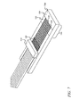
- the width of both the mesa 610 and the central ridge 620 may decrease gradually along the length of the taper, the width of the central ridge 620 decreasing to near zero (e.g., to a width between 100 nm and 1 micron) at an end of the central ridge 620 part-way along the taper or at the end of the taper.
- a sufficiently gradual taper may reduce the optical loss incurred by light propagating through the taper.
- the central ridge 620 extends over a length of between 2 mm and 7 mm (e.g., over a length of 5 mm) and the mesa 610 tapers from 24 microns to 13 microns over the same length.
- FIG. 8D illustrates an embodiment in which the chip-end waveguide facet 118 is set back from the step 845 at the edge of the mounting surface 720 of the interposer beam expander.
- FIG. 8D is not drawn to scale; for example, the amount by which the waveguide facet 118 is set back from the step 845 may be significantly smaller than that shown.
Landscapes
- Physics & Mathematics (AREA)
- General Physics & Mathematics (AREA)
- Optics & Photonics (AREA)
- Engineering & Computer Science (AREA)
- Microelectronics & Electronic Packaging (AREA)
- Optical Couplings Of Light Guides (AREA)
Abstract
Description
Claims (24)
Priority Applications (3)
| Application Number | Priority Date | Filing Date | Title |
|---|---|---|---|
| US14/789,489 US10317620B2 (en) | 2015-07-01 | 2015-07-01 | Interposer beam expander chip |
| GB1512931.5A GB2539971B (en) | 2015-07-01 | 2015-07-22 | Interposer beam expander chip |
| PCT/GB2016/052006 WO2017001869A1 (en) | 2015-07-01 | 2016-07-01 | Interposer beam expander chip |
Applications Claiming Priority (1)
| Application Number | Priority Date | Filing Date | Title |
|---|---|---|---|
| US14/789,489 US10317620B2 (en) | 2015-07-01 | 2015-07-01 | Interposer beam expander chip |
Publications (2)
| Publication Number | Publication Date |
|---|---|
| US20170003450A1 US20170003450A1 (en) | 2017-01-05 |
| US10317620B2 true US10317620B2 (en) | 2019-06-11 |
Family
ID=54064782
Family Applications (1)
| Application Number | Title | Priority Date | Filing Date |
|---|---|---|---|
| US14/789,489 Active 2036-02-15 US10317620B2 (en) | 2015-07-01 | 2015-07-01 | Interposer beam expander chip |
Country Status (3)
| Country | Link |
|---|---|
| US (1) | US10317620B2 (en) |
| GB (1) | GB2539971B (en) |
| WO (1) | WO2017001869A1 (en) |
Cited By (1)
| Publication number | Priority date | Publication date | Assignee | Title |
|---|---|---|---|---|
| US11133225B2 (en) * | 2016-07-13 | 2021-09-28 | Rockley Photonics Limited | Mode converter and method of fabricating thereof |
Families Citing this family (10)
| Publication number | Priority date | Publication date | Assignee | Title |
|---|---|---|---|---|
| US10877217B2 (en) | 2017-01-06 | 2020-12-29 | Rockley Photonics Limited | Copackaging of asic and silicon photonics |
| US9995881B1 (en) * | 2017-06-28 | 2018-06-12 | Cisco Technology, Inc. | TSV compatible fiber array coupler for silicon photonics |
| EP3662311A1 (en) * | 2017-08-01 | 2020-06-10 | Rockley Photonics Limited | Module with transmit optical subassembly and receive optical subassembly |
| CN118426119A (en) * | 2018-06-28 | 2024-08-02 | 3M创新有限公司 | Optical coupling element and assembly |
| EP3671297B1 (en) * | 2018-12-21 | 2025-02-26 | Adtran Networks SE | Electro-optical assembly |
| WO2020172585A1 (en) * | 2019-02-22 | 2020-08-27 | President And Fellows Of Harvard College | Low loss fiber-to-chip interfaces for lithium niobate photonic integrated circuits |
| US11762154B2 (en) | 2020-08-01 | 2023-09-19 | Ayar Labs, Inc. | Systems and methods for passively-aligned optical waveguide edge-coupling |
| US12444906B2 (en) * | 2022-06-28 | 2025-10-14 | Chong Zhang | Heterogeneously integrated photonic platform with improved thermal performance |
| CN115657225A (en) * | 2022-10-27 | 2023-01-31 | 西湖大学 | A fiber end face packaging method for a waveguide integrated optical chip |
| GB202316378D0 (en) * | 2023-10-26 | 2023-12-13 | Univ College Cork National Univ Of Ireland | Photonic integrated circuit micro-optical coupler for cryogenic environments |
Citations (28)
| Publication number | Priority date | Publication date | Assignee | Title |
|---|---|---|---|---|
| US5259049A (en) | 1991-09-19 | 1993-11-02 | International Business Machines Corporation | Self-aligned optical waveguide to laser structure and method for making the same |
| US5703895A (en) | 1994-05-02 | 1997-12-30 | France Telecom | Opto-electronic semiconductor device including an integrated mode transformer |
| US5787214A (en) | 1995-05-06 | 1998-07-28 | Bookham Technology Ltd. | Connection between an integrated optical waveguide and an optical fibre |
| US6108478A (en) | 1997-02-07 | 2000-08-22 | Bookham Technology Limited | Tapered rib waveguide |
| US6162653A (en) | 1998-07-30 | 2000-12-19 | Bookham Technology, Plc | Lead frame attachment for optoelectronic device |
| US6266468B1 (en) | 1998-06-12 | 2001-07-24 | Bookham Technology Plc | Waveguide end face |
| US20010031122A1 (en) | 1999-12-02 | 2001-10-18 | Lackritz Hilary S. | Photodefinition of optical devices |
| US6310995B1 (en) | 1998-11-25 | 2001-10-30 | University Of Maryland | Resonantly coupled waveguides using a taper |
| US6356692B1 (en) | 1999-02-04 | 2002-03-12 | Hitachi, Ltd. | Optical module, transmitter, receiver, optical switch, optical communication unit, add-and-drop multiplexing unit, and method for manufacturing the optical module |
| US20020051607A1 (en) | 2000-11-01 | 2002-05-02 | Tatemi Ido | Optical waveguide, optical module, and their fabrication method |
| WO2002075387A2 (en) | 2001-03-16 | 2002-09-26 | Bookham Technology Plc | A tapered optical waveguide |
| US6509139B1 (en) * | 1999-10-13 | 2003-01-21 | Bookham Technology Plc | Method of fabricating an integrated optical component |
| US20040114872A1 (en) | 2002-11-25 | 2004-06-17 | Matsushita Electric Industrial Co., Ltd. | Optical functional device and optical module |
| US20050129402A1 (en) | 2003-10-21 | 2005-06-16 | Kim Byoung W. | WDM-PON system with optical wavelength alignment function |
| US20070189688A1 (en) | 2006-02-15 | 2007-08-16 | Gabriel Dehlinger | Waveguide photodetector |
| US20080279505A1 (en) | 2007-05-09 | 2008-11-13 | Alcatel-Lucent. | Optical coupling structure |
| US7643710B1 (en) | 2008-09-17 | 2010-01-05 | Intel Corporation | Method and apparatus for efficient coupling between silicon photonic chip and optical fiber |
| US20100314027A1 (en) | 2001-10-30 | 2010-12-16 | Blauvelt Henry A | Optical junction apparatus and methods employing optical power transverse-transfer |
| WO2011044090A2 (en) | 2009-10-09 | 2011-04-14 | Corning Incorporated | Integrated silicon photonic active optical cable components, sub-assemblies and assemblies |
| US20110097033A1 (en) | 2009-10-26 | 2011-04-28 | United Microelectronics Corp. | Focusing member and optoelectronic device |
| US20120093456A1 (en) | 2010-10-14 | 2012-04-19 | Universiteit Gent | Coupling Methods and Systems Using a Taper |
| WO2012049273A1 (en) | 2010-10-14 | 2012-04-19 | Rwth Aachen | Laser to chip coupler |
| EP2535749A1 (en) | 2011-06-17 | 2012-12-19 | Caliopa NV | Optical interposer |
| EP2549328A1 (en) | 2011-07-21 | 2013-01-23 | Citizen Holdings Co., Ltd. | Optical module |
| US8798409B2 (en) | 2010-10-07 | 2014-08-05 | Alcatel Lucent | Optical transmitter with flip-chip mounted laser or integrated arrayed waveguide grating wavelenth division multiplexer |
| US20150010266A1 (en) | 2013-07-03 | 2015-01-08 | Cisco Technology, Inc. | Photonic integration platform |
| US20150055912A1 (en) * | 2013-08-23 | 2015-02-26 | Cisco Technology, Inc. | Coupling light from an external source to a waveguide using a multi-step converter |
| US20150219853A1 (en) | 2014-02-06 | 2015-08-06 | Skorpios Technologies, Inc. | Integrated multistage taper coupler for waveguide to fiber coupling |
-
2015
- 2015-07-01 US US14/789,489 patent/US10317620B2/en active Active
- 2015-07-22 GB GB1512931.5A patent/GB2539971B/en active Active
-
2016
- 2016-07-01 WO PCT/GB2016/052006 patent/WO2017001869A1/en not_active Ceased
Patent Citations (29)
| Publication number | Priority date | Publication date | Assignee | Title |
|---|---|---|---|---|
| US5259049A (en) | 1991-09-19 | 1993-11-02 | International Business Machines Corporation | Self-aligned optical waveguide to laser structure and method for making the same |
| US5703895A (en) | 1994-05-02 | 1997-12-30 | France Telecom | Opto-electronic semiconductor device including an integrated mode transformer |
| US5787214A (en) | 1995-05-06 | 1998-07-28 | Bookham Technology Ltd. | Connection between an integrated optical waveguide and an optical fibre |
| US6108478A (en) | 1997-02-07 | 2000-08-22 | Bookham Technology Limited | Tapered rib waveguide |
| US6266468B1 (en) | 1998-06-12 | 2001-07-24 | Bookham Technology Plc | Waveguide end face |
| US6162653A (en) | 1998-07-30 | 2000-12-19 | Bookham Technology, Plc | Lead frame attachment for optoelectronic device |
| US6310995B1 (en) | 1998-11-25 | 2001-10-30 | University Of Maryland | Resonantly coupled waveguides using a taper |
| US6356692B1 (en) | 1999-02-04 | 2002-03-12 | Hitachi, Ltd. | Optical module, transmitter, receiver, optical switch, optical communication unit, add-and-drop multiplexing unit, and method for manufacturing the optical module |
| US6509139B1 (en) * | 1999-10-13 | 2003-01-21 | Bookham Technology Plc | Method of fabricating an integrated optical component |
| US20010031122A1 (en) | 1999-12-02 | 2001-10-18 | Lackritz Hilary S. | Photodefinition of optical devices |
| US20020051607A1 (en) | 2000-11-01 | 2002-05-02 | Tatemi Ido | Optical waveguide, optical module, and their fabrication method |
| WO2002075387A2 (en) | 2001-03-16 | 2002-09-26 | Bookham Technology Plc | A tapered optical waveguide |
| US20100314027A1 (en) | 2001-10-30 | 2010-12-16 | Blauvelt Henry A | Optical junction apparatus and methods employing optical power transverse-transfer |
| US20040114872A1 (en) | 2002-11-25 | 2004-06-17 | Matsushita Electric Industrial Co., Ltd. | Optical functional device and optical module |
| US20050129402A1 (en) | 2003-10-21 | 2005-06-16 | Kim Byoung W. | WDM-PON system with optical wavelength alignment function |
| US20070189688A1 (en) | 2006-02-15 | 2007-08-16 | Gabriel Dehlinger | Waveguide photodetector |
| US20080279505A1 (en) | 2007-05-09 | 2008-11-13 | Alcatel-Lucent. | Optical coupling structure |
| US7643710B1 (en) | 2008-09-17 | 2010-01-05 | Intel Corporation | Method and apparatus for efficient coupling between silicon photonic chip and optical fiber |
| WO2011044090A2 (en) | 2009-10-09 | 2011-04-14 | Corning Incorporated | Integrated silicon photonic active optical cable components, sub-assemblies and assemblies |
| US20110097033A1 (en) | 2009-10-26 | 2011-04-28 | United Microelectronics Corp. | Focusing member and optoelectronic device |
| US8798409B2 (en) | 2010-10-07 | 2014-08-05 | Alcatel Lucent | Optical transmitter with flip-chip mounted laser or integrated arrayed waveguide grating wavelenth division multiplexer |
| WO2012049273A1 (en) | 2010-10-14 | 2012-04-19 | Rwth Aachen | Laser to chip coupler |
| US20130209112A1 (en) * | 2010-10-14 | 2013-08-15 | Rwth Aachen | Laser to Chip Coupler |
| US20120093456A1 (en) | 2010-10-14 | 2012-04-19 | Universiteit Gent | Coupling Methods and Systems Using a Taper |
| EP2535749A1 (en) | 2011-06-17 | 2012-12-19 | Caliopa NV | Optical interposer |
| EP2549328A1 (en) | 2011-07-21 | 2013-01-23 | Citizen Holdings Co., Ltd. | Optical module |
| US20150010266A1 (en) | 2013-07-03 | 2015-01-08 | Cisco Technology, Inc. | Photonic integration platform |
| US20150055912A1 (en) * | 2013-08-23 | 2015-02-26 | Cisco Technology, Inc. | Coupling light from an external source to a waveguide using a multi-step converter |
| US20150219853A1 (en) | 2014-02-06 | 2015-08-06 | Skorpios Technologies, Inc. | Integrated multistage taper coupler for waveguide to fiber coupling |
Non-Patent Citations (3)
| Title |
|---|
| International Search Report and Written Opinion of the International Searching Authority, dated Sep. 28, 2016, Corresponding to PCT/GB2016/052006, 12 pages. |
| UKIPO Search Report for Application No. GB1512931.5, dated Oct. 20, 2015, 2 pages. |
| UKIPO Search Report for Application No. GB1512931.5, dated Sep. 2, 2015, 5 pages. |
Cited By (1)
| Publication number | Priority date | Publication date | Assignee | Title |
|---|---|---|---|---|
| US11133225B2 (en) * | 2016-07-13 | 2021-09-28 | Rockley Photonics Limited | Mode converter and method of fabricating thereof |
Also Published As
| Publication number | Publication date |
|---|---|
| WO2017001869A1 (en) | 2017-01-05 |
| GB2539971B (en) | 2021-11-10 |
| US20170003450A1 (en) | 2017-01-05 |
| GB201512931D0 (en) | 2015-09-02 |
| GB2539971A (en) | 2017-01-04 |
Similar Documents
| Publication | Publication Date | Title |
|---|---|---|
| US20170003450A1 (en) | Interposer beam expander chip | |
| US6212320B1 (en) | Coupling optical fibre to waveguide | |
| US9857531B2 (en) | Optical component with angled-facet waveguide | |
| US9377587B2 (en) | Fiber optic coupler array | |
| CN101371175B (en) | Broadband Optical Coupling into Thin SOI CMOS Integrated Optical Circuits | |
| US20180031791A1 (en) | Electro-optical interconnect platform | |
| US7622708B2 (en) | Optical element for free-space propagation between an optical waveguide and another optical waveguide, component, or device | |
| US20150125110A1 (en) | Passively Placed Vertical Optical Connector | |
| US20130209033A1 (en) | Coupling between optical devices | |
| KR20200060718A (en) | Method and apparatus for self-aligning connection of optical fibers to waveguides of photonic integrated circuits | |
| EP1015922A1 (en) | A tapered rib waveguide | |
| US9274293B2 (en) | Arrangement of photonic chip and optical adaptor for coupling optical signals | |
| CN114690310A (en) | Edge coupler including a grooved film | |
| US6535685B1 (en) | Arcuate fiber routing using stepped grooves | |
| US20040247248A1 (en) | Passive alignment between waveguides and optical components | |
| US6819841B2 (en) | Self-aligned optical waveguide to optical fiber connection system | |
| JP7725960B2 (en) | Optical integrated device, optical integrated circuit wafer, and method for manufacturing optical integrated device | |
| WO2002075387A2 (en) | A tapered optical waveguide | |
| US20030215187A1 (en) | Waveguide to V-groove arrangement | |
| JP2004062064A (en) | Optical waveguide module and method for manufacturing optical waveguide substrate | |
| GB2381592A (en) | Optical device with recess for optical component |
Legal Events
| Date | Code | Title | Description |
|---|---|---|---|
| AS | Assignment |
Owner name: ROCKLEY PHOTONICS LIMITED, UNITED KINGDOM Free format text: ASSIGNMENT OF ASSIGNORS INTEREST;ASSIGNORS:RICKMAN, ANDREW GEORGE;ZILKIE, AARON;LEROSE, DAMIANA;AND OTHERS;SIGNING DATES FROM 20150813 TO 20150815;REEL/FRAME:036452/0925 |
|
| AS | Assignment |
Owner name: SILICON VALLEY BANK, CALIFORNIA Free format text: SECURITY INTEREST;ASSIGNOR:ROCKLEY PHOTONICS LIMITED;REEL/FRAME:041108/0640 Effective date: 20170127 |
|
| AS | Assignment |
Owner name: KREOS CAPITAL V (UK) LIMITED, UNITED KINGDOM Free format text: SECURITY INTEREST;ASSIGNOR:ROCKLEY PHOTONICS LIMITED;REEL/FRAME:042517/0968 Effective date: 20170526 |
|
| FEPP | Fee payment procedure |
Free format text: ENTITY STATUS SET TO UNDISCOUNTED (ORIGINAL EVENT CODE: BIG.); ENTITY STATUS OF PATENT OWNER: LARGE ENTITY |
|
| AS | Assignment |
Owner name: ROCKLEY PHOTONICS LIMITED, GREAT BRITAIN Free format text: ASSIGNMENT OF ASSIGNORS INTEREST;ASSIGNORS:RICKMAN, ANDREW;ROCKLEY VENTURES LIMITED;REEL/FRAME:044502/0741 Effective date: 20170910 |
|
| STPP | Information on status: patent application and granting procedure in general |
Free format text: NOTICE OF ALLOWANCE MAILED -- APPLICATION RECEIVED IN OFFICE OF PUBLICATIONS |
|
| STCF | Information on status: patent grant |
Free format text: PATENTED CASE |
|
| AS | Assignment |
Owner name: ROCKLEY PHOTONICS LIMITED, UNITED KINGDOM Free format text: RELEASE BY SECURED PARTY;ASSIGNOR:KREOS CAPITAL V (UK) LIMITED;REEL/FRAME:060116/0136 Effective date: 20220427 Owner name: ROCKLEY PHOTONICS LIMITED, UNITED KINGDOM Free format text: RELEASE BY SECURED PARTY;ASSIGNOR:SILICON VALLEY BANK;REEL/FRAME:059948/0387 Effective date: 20220427 |
|
| AS | Assignment |
Owner name: WILMINGTON SAVINGS FUND SOCIETY, FSB, AS COLLATERAL AGENT, DELAWARE Free format text: SECURITY INTEREST;ASSIGNOR:ROCKLEY PHOTONICS LIMITED;REEL/FRAME:060204/0749 Effective date: 20220527 |
|
| AS | Assignment |
Owner name: WILMINGTON SAVINGS FUND SOCIETY, FSB, AS COLLATERAL AGENT, DELAWARE Free format text: SECURITY INTEREST - SUPER SENIOR INDENTURE;ASSIGNOR:ROCKLEY PHOTONICS LIMITED;REEL/FRAME:061768/0082 Effective date: 20221025 |
|
| MAFP | Maintenance fee payment |
Free format text: PAYMENT OF MAINTENANCE FEE, 4TH YEAR, LARGE ENTITY (ORIGINAL EVENT CODE: M1551); ENTITY STATUS OF PATENT OWNER: LARGE ENTITY Year of fee payment: 4 |
|
| AS | Assignment |
Owner name: ROCKLEY PHOTONICS LIMITED, UNITED KINGDOM Free format text: RELEASE OF PATENT SECURITY INTEREST - SUPER SENIOR INDENTURE - REEL/FRAME 061768/0082;ASSIGNOR:WILMINGTON SAVINGS FUND SOCIETY, FSB, AS COLLATERAL AGENT;REEL/FRAME:063264/0416 Effective date: 20230314 Owner name: ROCKLEY PHOTONICS LIMITED, UNITED KINGDOM Free format text: RELEASE OF SECURITY INTEREST - REEL/FRAME 060204/0749;ASSIGNOR:WILMINGTON SAVINGS FUND SOCIETY, FSB, AS COLLATERAL AGENT;REEL/FRAME:063264/0333 Effective date: 20230314 Owner name: WILMINGTON SAVINGS FUND SOCIETY, FSB, AS COLLATERAL AGENT, DELAWARE Free format text: SECURITY INTEREST;ASSIGNOR:ROCKLEY PHOTONICS LIMITED;REEL/FRAME:063287/0879 Effective date: 20230314 |