US10312378B2 - Lateral gallium nitride JFET with controlled doping profile - Google Patents
Lateral gallium nitride JFET with controlled doping profile Download PDFInfo
- Publication number
- US10312378B2 US10312378B2 US15/882,955 US201815882955A US10312378B2 US 10312378 B2 US10312378 B2 US 10312378B2 US 201815882955 A US201815882955 A US 201815882955A US 10312378 B2 US10312378 B2 US 10312378B2
- Authority
- US
- United States
- Prior art keywords
- dopant concentration
- semiconductor layer
- layer
- substrate
- conductivity type
- Prior art date
- Legal status (The legal status is an assumption and is not a legal conclusion. Google has not performed a legal analysis and makes no representation as to the accuracy of the status listed.)
- Active
Links
- JMASRVWKEDWRBT-UHFFFAOYSA-N Gallium nitride Chemical compound [Ga]#N JMASRVWKEDWRBT-UHFFFAOYSA-N 0.000 title description 64
- 229910002601 GaN Inorganic materials 0.000 title description 31
- 239000004065 semiconductor Substances 0.000 claims abstract description 200
- 239000002019 doping agent Substances 0.000 claims abstract description 157
- 239000000758 substrate Substances 0.000 claims abstract description 79
- 230000005669 field effect Effects 0.000 claims abstract description 22
- 230000007423 decrease Effects 0.000 claims description 11
- 230000003247 decreasing effect Effects 0.000 claims description 7
- 239000010410 layer Substances 0.000 description 403
- 238000000034 method Methods 0.000 description 60
- 230000008569 process Effects 0.000 description 43
- 239000013078 crystal Substances 0.000 description 23
- BOTDANWDWHJENH-UHFFFAOYSA-N Tetraethyl orthosilicate Chemical compound CCO[Si](OCC)(OCC)OCC BOTDANWDWHJENH-UHFFFAOYSA-N 0.000 description 20
- 229910021420 polycrystalline silicon Inorganic materials 0.000 description 20
- 229920005591 polysilicon Polymers 0.000 description 18
- 238000005468 ion implantation Methods 0.000 description 17
- 239000000463 material Substances 0.000 description 15
- VYPSYNLAJGMNEJ-UHFFFAOYSA-N Silicium dioxide Chemical compound O=[Si]=O VYPSYNLAJGMNEJ-UHFFFAOYSA-N 0.000 description 14
- XUIMIQQOPSSXEZ-UHFFFAOYSA-N Silicon Chemical compound [Si] XUIMIQQOPSSXEZ-UHFFFAOYSA-N 0.000 description 13
- 229910052710 silicon Inorganic materials 0.000 description 13
- 239000010703 silicon Substances 0.000 description 13
- 230000004888 barrier function Effects 0.000 description 12
- 238000004519 manufacturing process Methods 0.000 description 12
- 229910052581 Si3N4 Inorganic materials 0.000 description 10
- 229910021421 monocrystalline silicon Inorganic materials 0.000 description 10
- HQVNEWCFYHHQES-UHFFFAOYSA-N silicon nitride Chemical compound N12[Si]34N5[Si]62N3[Si]51N64 HQVNEWCFYHHQES-UHFFFAOYSA-N 0.000 description 10
- PMHQVHHXPFUNSP-UHFFFAOYSA-M copper(1+);methylsulfanylmethane;bromide Chemical compound Br[Cu].CSC PMHQVHHXPFUNSP-UHFFFAOYSA-M 0.000 description 9
- 238000004518 low pressure chemical vapour deposition Methods 0.000 description 9
- 239000007943 implant Substances 0.000 description 8
- 230000003746 surface roughness Effects 0.000 description 8
- 238000010586 diagram Methods 0.000 description 7
- 238000012986 modification Methods 0.000 description 7
- 230000004048 modification Effects 0.000 description 7
- 229910052814 silicon oxide Inorganic materials 0.000 description 7
- KRHYYFGTRYWZRS-UHFFFAOYSA-N Fluorane Chemical compound F KRHYYFGTRYWZRS-UHFFFAOYSA-N 0.000 description 6
- 238000000151 deposition Methods 0.000 description 6
- 229910052751 metal Inorganic materials 0.000 description 6
- 239000002184 metal Substances 0.000 description 6
- 235000012431 wafers Nutrition 0.000 description 6
- 230000015556 catabolic process Effects 0.000 description 5
- 229910010293 ceramic material Inorganic materials 0.000 description 5
- 230000008021 deposition Effects 0.000 description 5
- 230000005684 electric field Effects 0.000 description 5
- 230000003647 oxidation Effects 0.000 description 5
- 238000007254 oxidation reaction Methods 0.000 description 5
- 238000012545 processing Methods 0.000 description 5
- ZOXJGFHDIHLPTG-UHFFFAOYSA-N Boron Chemical compound [B] ZOXJGFHDIHLPTG-UHFFFAOYSA-N 0.000 description 4
- 239000002253 acid Substances 0.000 description 4
- 230000008901 benefit Effects 0.000 description 4
- 229910052796 boron Inorganic materials 0.000 description 4
- 229910000040 hydrogen fluoride Inorganic materials 0.000 description 4
- 239000011229 interlayer Substances 0.000 description 4
- 238000005304 joining Methods 0.000 description 4
- 239000000377 silicon dioxide Substances 0.000 description 4
- 239000002356 single layer Substances 0.000 description 4
- 229910052681 coesite Inorganic materials 0.000 description 3
- 239000004020 conductor Substances 0.000 description 3
- 229910052906 cristobalite Inorganic materials 0.000 description 3
- 238000005137 deposition process Methods 0.000 description 3
- 238000009792 diffusion process Methods 0.000 description 3
- -1 e.g. Substances 0.000 description 3
- 238000009499 grossing Methods 0.000 description 3
- 238000002513 implantation Methods 0.000 description 3
- 239000011777 magnesium Substances 0.000 description 3
- SIWVEOZUMHYXCS-UHFFFAOYSA-N oxo(oxoyttriooxy)yttrium Chemical compound O=[Y]O[Y]=O SIWVEOZUMHYXCS-UHFFFAOYSA-N 0.000 description 3
- 229910052682 stishovite Inorganic materials 0.000 description 3
- 238000012546 transfer Methods 0.000 description 3
- 229910052905 tridymite Inorganic materials 0.000 description 3
- PIGFYZPCRLYGLF-UHFFFAOYSA-N Aluminum nitride Chemical compound [Al]#N PIGFYZPCRLYGLF-UHFFFAOYSA-N 0.000 description 2
- RYGMFSIKBFXOCR-UHFFFAOYSA-N Copper Chemical compound [Cu] RYGMFSIKBFXOCR-UHFFFAOYSA-N 0.000 description 2
- UFHFLCQGNIYNRP-UHFFFAOYSA-N Hydrogen Chemical compound [H][H] UFHFLCQGNIYNRP-UHFFFAOYSA-N 0.000 description 2
- FYYHWMGAXLPEAU-UHFFFAOYSA-N Magnesium Chemical compound [Mg] FYYHWMGAXLPEAU-UHFFFAOYSA-N 0.000 description 2
- QVGXLLKOCUKJST-UHFFFAOYSA-N atomic oxygen Chemical compound [O] QVGXLLKOCUKJST-UHFFFAOYSA-N 0.000 description 2
- 230000015572 biosynthetic process Effects 0.000 description 2
- 230000000903 blocking effect Effects 0.000 description 2
- 239000000919 ceramic Substances 0.000 description 2
- 230000008859 change Effects 0.000 description 2
- 238000003776 cleavage reaction Methods 0.000 description 2
- 229910052802 copper Inorganic materials 0.000 description 2
- 239000010949 copper Substances 0.000 description 2
- 230000007547 defect Effects 0.000 description 2
- 238000007598 dipping method Methods 0.000 description 2
- 238000005530 etching Methods 0.000 description 2
- 229910052739 hydrogen Inorganic materials 0.000 description 2
- 239000001257 hydrogen Substances 0.000 description 2
- 239000012535 impurity Substances 0.000 description 2
- 230000000670 limiting effect Effects 0.000 description 2
- 229910052749 magnesium Inorganic materials 0.000 description 2
- 239000007769 metal material Substances 0.000 description 2
- 238000010943 off-gassing Methods 0.000 description 2
- 230000003287 optical effect Effects 0.000 description 2
- 229910052760 oxygen Inorganic materials 0.000 description 2
- 239000001301 oxygen Substances 0.000 description 2
- 230000002441 reversible effect Effects 0.000 description 2
- 230000007017 scission Effects 0.000 description 2
- 239000011573 trace mineral Substances 0.000 description 2
- 235000013619 trace mineral Nutrition 0.000 description 2
- RUDFQVOCFDJEEF-UHFFFAOYSA-N yttrium(III) oxide Inorganic materials [O-2].[O-2].[O-2].[Y+3].[Y+3] RUDFQVOCFDJEEF-UHFFFAOYSA-N 0.000 description 2
- 229910000577 Silicon-germanium Inorganic materials 0.000 description 1
- BQCADISMDOOEFD-UHFFFAOYSA-N Silver Chemical compound [Ag] BQCADISMDOOEFD-UHFFFAOYSA-N 0.000 description 1
- RTAQQCXQSZGOHL-UHFFFAOYSA-N Titanium Chemical compound [Ti] RTAQQCXQSZGOHL-UHFFFAOYSA-N 0.000 description 1
- 230000002411 adverse Effects 0.000 description 1
- 229910052782 aluminium Inorganic materials 0.000 description 1
- XAGFODPZIPBFFR-UHFFFAOYSA-N aluminium Chemical compound [Al] XAGFODPZIPBFFR-UHFFFAOYSA-N 0.000 description 1
- 238000000137 annealing Methods 0.000 description 1
- 239000011230 binding agent Substances 0.000 description 1
- 150000001875 compounds Chemical class 0.000 description 1
- 238000010276 construction Methods 0.000 description 1
- 229910003460 diamond Inorganic materials 0.000 description 1
- 239000010432 diamond Substances 0.000 description 1
- 238000009826 distribution Methods 0.000 description 1
- 238000005516 engineering process Methods 0.000 description 1
- QZQVBEXLDFYHSR-UHFFFAOYSA-N gallium(III) oxide Inorganic materials O=[Ga]O[Ga]=O QZQVBEXLDFYHSR-UHFFFAOYSA-N 0.000 description 1
- PCHJSUWPFVWCPO-UHFFFAOYSA-N gold Chemical compound [Au] PCHJSUWPFVWCPO-UHFFFAOYSA-N 0.000 description 1
- 229910052737 gold Inorganic materials 0.000 description 1
- 239000010931 gold Substances 0.000 description 1
- 150000002500 ions Chemical class 0.000 description 1
- 230000000873 masking effect Effects 0.000 description 1
- 230000003278 mimic effect Effects 0.000 description 1
- 229910003465 moissanite Inorganic materials 0.000 description 1
- 239000002245 particle Substances 0.000 description 1
- 238000002161 passivation Methods 0.000 description 1
- 230000000704 physical effect Effects 0.000 description 1
- 238000000623 plasma-assisted chemical vapour deposition Methods 0.000 description 1
- 238000005498 polishing Methods 0.000 description 1
- 230000002829 reductive effect Effects 0.000 description 1
- 230000008439 repair process Effects 0.000 description 1
- 229910052594 sapphire Inorganic materials 0.000 description 1
- 239000010980 sapphire Substances 0.000 description 1
- 229910010271 silicon carbide Inorganic materials 0.000 description 1
- 235000012239 silicon dioxide Nutrition 0.000 description 1
- 229910052709 silver Inorganic materials 0.000 description 1
- 239000004332 silver Substances 0.000 description 1
- 239000000126 substance Substances 0.000 description 1
- 238000012360 testing method Methods 0.000 description 1
- 239000010936 titanium Substances 0.000 description 1
- 229910052719 titanium Inorganic materials 0.000 description 1
- 238000009966 trimming Methods 0.000 description 1
- WFKWXMTUELFFGS-UHFFFAOYSA-N tungsten Chemical compound [W] WFKWXMTUELFFGS-UHFFFAOYSA-N 0.000 description 1
- 229910052721 tungsten Inorganic materials 0.000 description 1
- 239000010937 tungsten Substances 0.000 description 1
- XLOMVQKBTHCTTD-UHFFFAOYSA-N zinc oxide Inorganic materials [Zn]=O XLOMVQKBTHCTTD-UHFFFAOYSA-N 0.000 description 1
Images


Classifications
-
- H01L29/808—
-
- H—ELECTRICITY
- H10—SEMICONDUCTOR DEVICES; ELECTRIC SOLID-STATE DEVICES NOT OTHERWISE PROVIDED FOR
- H10D—INORGANIC ELECTRIC SEMICONDUCTOR DEVICES
- H10D30/00—Field-effect transistors [FET]
- H10D30/80—FETs having rectifying junction gate electrodes
- H10D30/83—FETs having PN junction gate electrodes
-
- H01L29/0615—
-
- H01L29/0649—
-
- H01L29/0847—
-
- H01L29/1058—
-
- H01L29/1066—
-
- H01L29/12—
-
- H01L29/2003—
-
- H01L29/36—
-
- H01L29/41775—
-
- H01L29/42312—
-
- H01L29/66446—
-
- H01L29/66893—
-
- H—ELECTRICITY
- H10—SEMICONDUCTOR DEVICES; ELECTRIC SOLID-STATE DEVICES NOT OTHERWISE PROVIDED FOR
- H10D—INORGANIC ELECTRIC SEMICONDUCTOR DEVICES
- H10D30/00—Field-effect transistors [FET]
- H10D30/01—Manufacture or treatment
-
- H—ELECTRICITY
- H10—SEMICONDUCTOR DEVICES; ELECTRIC SOLID-STATE DEVICES NOT OTHERWISE PROVIDED FOR
- H10D—INORGANIC ELECTRIC SEMICONDUCTOR DEVICES
- H10D30/00—Field-effect transistors [FET]
- H10D30/01—Manufacture or treatment
- H10D30/051—Manufacture or treatment of FETs having PN junction gates
-
- H—ELECTRICITY
- H10—SEMICONDUCTOR DEVICES; ELECTRIC SOLID-STATE DEVICES NOT OTHERWISE PROVIDED FOR
- H10D—INORGANIC ELECTRIC SEMICONDUCTOR DEVICES
- H10D62/00—Semiconductor bodies, or regions thereof, of devices having potential barriers
- H10D62/10—Shapes, relative sizes or dispositions of the regions of the semiconductor bodies; Shapes of the semiconductor bodies
- H10D62/102—Constructional design considerations for preventing surface leakage or controlling electric field concentration
- H10D62/103—Constructional design considerations for preventing surface leakage or controlling electric field concentration for increasing or controlling the breakdown voltage of reverse-biased devices
- H10D62/105—Constructional design considerations for preventing surface leakage or controlling electric field concentration for increasing or controlling the breakdown voltage of reverse-biased devices by having particular doping profiles, shapes or arrangements of PN junctions; by having supplementary regions, e.g. junction termination extension [JTE]
-
- H—ELECTRICITY
- H10—SEMICONDUCTOR DEVICES; ELECTRIC SOLID-STATE DEVICES NOT OTHERWISE PROVIDED FOR
- H10D—INORGANIC ELECTRIC SEMICONDUCTOR DEVICES
- H10D62/00—Semiconductor bodies, or regions thereof, of devices having potential barriers
- H10D62/10—Shapes, relative sizes or dispositions of the regions of the semiconductor bodies; Shapes of the semiconductor bodies
- H10D62/113—Isolations within a component, i.e. internal isolations
- H10D62/115—Dielectric isolations, e.g. air gaps
-
- H—ELECTRICITY
- H10—SEMICONDUCTOR DEVICES; ELECTRIC SOLID-STATE DEVICES NOT OTHERWISE PROVIDED FOR
- H10D—INORGANIC ELECTRIC SEMICONDUCTOR DEVICES
- H10D62/00—Semiconductor bodies, or regions thereof, of devices having potential barriers
- H10D62/10—Shapes, relative sizes or dispositions of the regions of the semiconductor bodies; Shapes of the semiconductor bodies
- H10D62/13—Semiconductor regions connected to electrodes carrying current to be rectified, amplified or switched, e.g. source or drain regions
- H10D62/149—Source or drain regions of field-effect devices
- H10D62/151—Source or drain regions of field-effect devices of IGFETs
-
- H—ELECTRICITY
- H10—SEMICONDUCTOR DEVICES; ELECTRIC SOLID-STATE DEVICES NOT OTHERWISE PROVIDED FOR
- H10D—INORGANIC ELECTRIC SEMICONDUCTOR DEVICES
- H10D62/00—Semiconductor bodies, or regions thereof, of devices having potential barriers
- H10D62/10—Shapes, relative sizes or dispositions of the regions of the semiconductor bodies; Shapes of the semiconductor bodies
- H10D62/17—Semiconductor regions connected to electrodes not carrying current to be rectified, amplified or switched, e.g. channel regions
- H10D62/213—Channel regions of field-effect devices
- H10D62/221—Channel regions of field-effect devices of FETs
- H10D62/328—Channel regions of field-effect devices of FETs having PN junction gates
-
- H—ELECTRICITY
- H10—SEMICONDUCTOR DEVICES; ELECTRIC SOLID-STATE DEVICES NOT OTHERWISE PROVIDED FOR
- H10D—INORGANIC ELECTRIC SEMICONDUCTOR DEVICES
- H10D62/00—Semiconductor bodies, or regions thereof, of devices having potential barriers
- H10D62/10—Shapes, relative sizes or dispositions of the regions of the semiconductor bodies; Shapes of the semiconductor bodies
- H10D62/17—Semiconductor regions connected to electrodes not carrying current to be rectified, amplified or switched, e.g. channel regions
- H10D62/343—Gate regions of field-effect devices having PN junction gates
-
- H—ELECTRICITY
- H10—SEMICONDUCTOR DEVICES; ELECTRIC SOLID-STATE DEVICES NOT OTHERWISE PROVIDED FOR
- H10D—INORGANIC ELECTRIC SEMICONDUCTOR DEVICES
- H10D62/00—Semiconductor bodies, or regions thereof, of devices having potential barriers
- H10D62/60—Impurity distributions or concentrations
-
- H—ELECTRICITY
- H10—SEMICONDUCTOR DEVICES; ELECTRIC SOLID-STATE DEVICES NOT OTHERWISE PROVIDED FOR
- H10D—INORGANIC ELECTRIC SEMICONDUCTOR DEVICES
- H10D62/00—Semiconductor bodies, or regions thereof, of devices having potential barriers
- H10D62/80—Semiconductor bodies, or regions thereof, of devices having potential barriers characterised by the materials
- H10D62/81—Semiconductor bodies, or regions thereof, of devices having potential barriers characterised by the materials of structures exhibiting quantum-confinement effects, e.g. single quantum wells; of structures having periodic or quasi-periodic potential variation
-
- H—ELECTRICITY
- H10—SEMICONDUCTOR DEVICES; ELECTRIC SOLID-STATE DEVICES NOT OTHERWISE PROVIDED FOR
- H10D—INORGANIC ELECTRIC SEMICONDUCTOR DEVICES
- H10D62/00—Semiconductor bodies, or regions thereof, of devices having potential barriers
- H10D62/80—Semiconductor bodies, or regions thereof, of devices having potential barriers characterised by the materials
- H10D62/85—Semiconductor bodies, or regions thereof, of devices having potential barriers characterised by the materials being Group III-V materials, e.g. GaAs
- H10D62/8503—Nitride Group III-V materials, e.g. AlN or GaN
-
- H—ELECTRICITY
- H10—SEMICONDUCTOR DEVICES; ELECTRIC SOLID-STATE DEVICES NOT OTHERWISE PROVIDED FOR
- H10D—INORGANIC ELECTRIC SEMICONDUCTOR DEVICES
- H10D64/00—Electrodes of devices having potential barriers
- H10D64/20—Electrodes characterised by their shapes, relative sizes or dispositions
- H10D64/23—Electrodes carrying the current to be rectified, amplified, oscillated or switched, e.g. sources, drains, anodes or cathodes
- H10D64/251—Source or drain electrodes for field-effect devices
- H10D64/258—Source or drain electrodes for field-effect devices characterised by the relative positions of the source or drain electrodes with respect to the gate electrode
-
- H—ELECTRICITY
- H10—SEMICONDUCTOR DEVICES; ELECTRIC SOLID-STATE DEVICES NOT OTHERWISE PROVIDED FOR
- H10D—INORGANIC ELECTRIC SEMICONDUCTOR DEVICES
- H10D64/00—Electrodes of devices having potential barriers
- H10D64/20—Electrodes characterised by their shapes, relative sizes or dispositions
- H10D64/27—Electrodes not carrying the current to be rectified, amplified, oscillated or switched, e.g. gates
- H10D64/311—Gate electrodes for field-effect devices
Definitions
- the present invention relates to semiconductor technology, and more particularly to a lateral GaN junction field-effect transistor (FET) and the method of forming the same.
- FET lateral GaN junction field-effect transistor
- the gate junction is usually biased at a high voltage in order to obtain high output power.
- a large electric field is formed in the channel below the gate edge on the drain side.
- Such a large electric field may result in a breakdown in the channel region between the gate and the drain electrode.
- HEMT high-electron mobility transistor
- Embodiments of the present disclosure provide a lateral junction field-effect transistor that has a controlled doping profile that can reduce the electric field and increase the breakdown voltage.
- One advantage of the present disclosure is to keep the maximum electric field away from the surface of the transistor so that the surface passivation and the field plate can be reduced or eliminated.
- Embodiments of the present disclosure provide a lateral junction field-effect transistor.
- the lateral junction field-effect transistor includes a substrate of a first conductivity type having a dopant concentration; a first semiconductor layer of the first conductivity type having a first dopant concentration lower than the dopant concentration and disposed on the substrate; a second semiconductor layer of a second conductivity type having a second dopant concentration, the second conductivity being different from the first conductivity type, the second semiconductor layer disposed on the first semiconductor layer; a third semiconductor layer of the first conductivity type having a third dopant concentration, the third semiconductor layer disposed on the second semiconductor layer; a fourth semiconductor layer of the first conductivity type having a fourth dopant concentration lower than the dopant concentration, the fourth semiconductor layer disposed on the third semiconductor layer; a source region and a drain region disposed in the second semiconductor layer and on opposite sides of the third semiconductor layer.
- Embodiments of the present disclosure also provide a method of manufacturing a semiconductor device.
- the method may include providing a substrate of a first conductivity type having a dopant concentration; forming a first semiconductor layer of the first conductivity type having a first dopant concentration on the substrate, the first dopant concentration being lower than the dopant concentration of the substrate; forming a second semiconductor layer of a second conductivity type having a second dopant concentration on the substrate; forming a third semiconductor layer of the first conductivity type having a third dopant concentration on the second semiconductor layer; forming a fourth semiconductor layer of the first conductivity type having a third dopant concentration on the second semiconductor layer; and forming electric contacts on the second and fourth semiconductor layers.
- FIG. 1 is a cross-sectional view illustrating a lateral junction field-effect transistor according to one embodiment of the present disclosure.
- FIG. 2 is a cross-sectional view illustrating a lateral junction field-effect transistor according to another embodiment of the present disclosure.
- FIG. 3A is a graph illustrating a doping profile of a semiconductor layer according to one embodiment of the present disclosure.
- FIG. 3B is a graph showing a doping profile of a semiconductor layer according to another embodiment of the present disclosure.
- FIG. 3C is a cross-sectional view of an exemplary doping profile of a portion of a semiconductor layer according to one embodiment of the present disclosure.
- FIG. 3D is a cross-sectional view of an exemplary doping profile of a portion of a semiconductor layer according to one embodiment of the present disclosure.
- FIG. 4 is a flowchart of a manufacturing method of a semiconductor device according to one embodiment of the present disclosure.
- FIGS. 5A-5F are cross-sectional views illustrating intermediate stages of a semiconductor device in a manufacturing method according to one embodiment of the present invention.
- FIG. 6 is a cross-sectional view of a hardmask according to one embodiment of the present invention.
- FIG. 7 is a graph illustrating a doping profile of a semiconductor layer according to one embodiment of the present disclosure.
- FIG. 8 is a simplified schematic diagram illustrating an engineered substrate structure according to an embodiment of the present disclosure.
- FIG. 9 is a simplified schematic diagram illustrating an engineered substrate structure according to some other embodiments of the present invention.
- FIG. 10 is a simplified schematic diagram illustrating an engineered substrate structure according to some further embodiments of the present invention.
- FIG. 11 is a simplified flowchart illustrating a method of fabricating an engineered substrate according to some embodiments of the present invention.
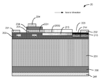
- FIG. 1 is a cross-sectional view illustrating a gallium nitride (GaN) lateral junction field-effect transistor 10 according to one embodiment of the present disclosure.
- lateral junction field-effect transistor (LJFET) 10 includes a substrate 100 of a first conductivity type having a high dopant concentration.
- substrate 100 is a GaN substrate having a high concentration of p-type dopants. The dopant concentration is uniformly distributed in substrate 100 .
- LJFET 10 also includes a first semiconductor layer 101 on substrate 100 , first semiconductor layer 101 includes GaN that may be epitaxially formed on substrate 100 and includes the first conductivity type having a first dopant concentration that is lower than the dopant concentration of substrate 100 .
- LJFET 10 also includes a second semiconductor layer 102 of a second conductivity type having a second dopant concentration on first semiconductor layer 101 , the second conductivity type is different form the first conductivity type. For example, if the first conductivity type is p-type, the second conductivity type is n-type, and vice versa. Second semiconductor layer 102 may be epitaxially formed on first semiconductor layer 101 and doped with n-type dopants.
- LJFET 10 also includes a third semiconductor layer 103 of the first conductivity type having a third dopant concentration on second semiconductor layer 102 .
- LJFET 10 further includes a fourth semiconductor layer 104 of the first conductivity type having a fourth dopant concentration on third semiconductor layer 103 .
- substrate 100 is a GaN substrate doped with p-type dopants having the high dopant concentration in the range between 1 ⁇ 10 19 atoms/cm 3 and 5 ⁇ 10 19 atoms/cm 3 , preferably 2 ⁇ 10 19 atoms/cm 3 .
- First semiconductor layer 101 is a GaN substrate doped with p-type dopants having the first dopant concentration in the range between 5 ⁇ 10 17 atoms/cm 3 and 5 ⁇ 10 18 atoms/cm 3 , preferably 1 ⁇ 10 18 atoms/cm 3 .
- Second semiconductor layer 102 is a GaN substrate doped with n-type dopants having the second dopant concentration in the range between 5 ⁇ 10 15 atoms/cm 3 and 5 ⁇ 10 16 atoms/cm 3 , preferably 2 ⁇ 10 16 atoms/cm 3 .
- Third semiconductor layer 103 is a GaN substrate doped with p-type dopants having the third dopant concentration in the range between 1 ⁇ 10 15 atoms/cm 3 and 9 ⁇ 10 15 atoms/cm 3 , preferably 4 ⁇ 10 15 atoms/cm 3 .
- Fourth semiconductor layer 104 is a GaN substrate doped with p-type dopants having the fourth dopant concentration in the range between 5 ⁇ 10 17 atoms/cm 3 and 5 ⁇ 10 18 atoms/cm 3 , preferably 1 ⁇ 10 18 atoms/cm 3 .
- the first and fourth semiconductor layers may have the same dopant concentration.
- the dopant concentration of the first and fourth semiconductor layers is about 1 ⁇ 10 18 atoms/cm 3 .
- third semiconductor layer 103 is a blocking layer disposed between second semiconductor layer 102 and fourth semiconductor layer 104 and has a dopant concentration in the range between 5 ⁇ 10 15 atoms/cm 3 and 5 ⁇ 10 16 atoms/cm 3 , preferably 2 ⁇ 10 16 atoms/cm 3 .
- Fourth semiconductor layer 104 is a gate layer and may have the same conductivity type and the same dopant concentration as those of substrate 100 .
- second semiconductor layer 102 includes a source region 111 , a drain region 112 , and a channel region 113 that is disposed below the fourth semiconductor layer (gate layer) and between source region 111 and drain region 112 .
- Second semiconductor layer 102 also includes a portion 114 below a portion of the third layer and between channel region 113 and drain region 112 .
- the channel region has a thickness of about 1.2 um and a dopant concentration of 2 ⁇ 10 16 atoms/cm 3
- the fourth semiconductor layer is a gate having a length of about 3 um and a dopant concentration of 1 ⁇ 10 18 atoms/cm 3 .
- Third semiconductor layer 103 is the blocking layer and has a thickness of about 16 um and a dopant concentration of 4 ⁇ 10 15 atoms/cm 3 .
- LJFET 10 also includes a source electrode 131 in contact with source region 111 , a drain electrode 132 in contact with drain region 112 , and a gate electrode 134 in contact with fourth semiconductor layer 104 .
- the source, drain and gate electrodes are made of a metal material, e.g., copper, aluminum, tungsten, silver, gold, or a combination thereof.
- LJFET 10 also includes a backside source electrode 141 disposed on the backside of substrate 100 .
- Backside source electrode 141 is a metal layer disposed along the bottom of LJFET 10 and is connected to source electrode 131 through a metal plug (i.e., a through-hole via).
- a through-hole via may be formed through the substrate, the first and second semiconductors layers and may be filled with a conductive material.
- Backside source electrode 141 is configured to be a thermal ground for dissipating heat of LJFET 10 .
- FIG. 2 is a cross-sectional view illustrating a lateral junction field-effect transistor 20 according to another embodiment of the present disclosure.
- Lateral junction field-effect transistor (LJFET) 20 is similar to LJFET 10 in FIG. 1 with the differences that the dopant concentrations of the second and third semiconductor layers are not uniformly distributed.
- LJFET 20 includes a substrate 200 of a first conductivity type having a high dopant concentration (e.g., 2 ⁇ 10 19 atoms/cm 3 ).
- substrate 200 is a highly doped p-type GaN substrate (referred herein as p GaN substrate).
- LJFET 20 further includes a first semiconductor layer 201 of the first conductivity type on substrate 200 .
- first semiconductor layer 201 may be an epitaxially formed p-type GaN layer having a first dopant concentration lower than that of the p GaN substrate.
- first semiconductor layer 201 may be formed out of substrate 200 by implanting n-type dopants into the highly doped substrate so that its dopant concentration is lower than the dopant concentration of the substrate.
- Epitaxially formed first semiconductor layer 201 is referred to as a p-GaN layer.
- LJFET 20 further includes a second semiconductor layer 202 of a second conductivity type having a second dopant concentration on first semiconductor layer 201 , the second conductivity type is different from the first conductivity type, second semiconductor layer 202 is an epitaxially formed n-type GaN layer (referred to as an n-GaN layer).
- LJFET 20 further includes a third semiconductor layer 203 of the first conductivity type having a third dopant concentration on second semiconductor layer 202 , third semiconductor layer 203 is referred to as a p-blocking layer.
- LJFET 20 further includes a fourth semiconductor layer 204 of the first conductivity type having a fourth dopant concentration on third semiconductor layer 203 , fourth semiconductor layer 204 is referred to as a gate layer.
- fourth semiconductor layer 203 covers a portion of the surface of the third semiconductor layer. In another embodiment, fourth layer 203 covers the entire surface of the third semiconductor layer.
- third semiconductor layer 203 includes a first portion 2031 disposed below fourth semiconductor layer (i.e., gate layer) 204 , and a second portion 2032 that is not covered by the fourth semiconductor layer.
- First portion 2031 has a uniformly distributed dopant concentration
- second portion 2032 has a gradually decreasing dopant concentration in the lateral direction toward the drain region. This dopant concentration form a higher level to a lower level will reduce the electric field formed between the gate and the drain.
- first portion 2031 has a uniform dopant concentration of 2 ⁇ 10 19 atoms/cm 3
- second portion 2032 has a dopant concentration having 2 ⁇ 10 19 atoms/cm 3 , which gradually decreases to 0 in the lateral direction to the distal end of third semiconductor layer 203
- first portion 2031 has a uniform dopant concentration of 2 ⁇ 10 19 atoms/cm 3
- second portion 2032 has a dopant concentration having 2 ⁇ 10 19 atoms/cm 3 , which stepwise decreases to 0 in the lateral direction to the distal end of third semiconductor layer 203 .
- LJFET 20 also includes a gate electrode 234 on fourth semiconductor layer (gate layer) 204 , a source electrode 231 and a drain electrode 232 disposed on second semiconductor layer 202 on opposite sides of fourth semiconductor layer 204 . There is an air gap 223 between the edge of the third semiconductor layer and the drain electrode 232
- second semiconductor layer 202 includes a first portion 211 configured as a source region, a second portion 212 below the fourth layer (i.e., below first portion 2031 of third semiconductor layer 203 ) configured as a channel region, a third portion 213 below a portion of third semiconductor layer that is not covered by the forth semiconductor layer (i.e., below second portion 2032 of third semiconductor layer 203 ), a third portion 214 adjacent to air gap 223 between the third semiconductor layer and the drain electrode, and a fourth portion 215 below the drain electrode.
- first portion 211 of semiconductor layer 202 has a dopant concentration of about 3 ⁇ 10 18 atoms/cm 3 ; second portion 212 has a dopant concentration of about 2 ⁇ 10 16 atoms/cm 3 ; and third portion 213 has a dopant concentration of about 6 ⁇ 10 16 atoms/cm 3 .
- the dopant concentration of first, second, and third portions is uniform, i.e., it does not change across the portion.
- Fourth portion 214 and fifth portion 215 each have a dopant concentration that decreases in a stepwise manner in the direction toward the substrate.
- the dopant concentration of fourth portion 214 decreases in a stepwise manner in the vertical direction (from top to bottom) from 3 ⁇ 10 18 atoms/cm 3 to 2 ⁇ 10 17 atoms/cm 3
- the dopant concentration of fifth portion 215 decreases in a stepwise manner in the vertical direction (from top to bottom) from 3 ⁇ 10 18 atoms/cm 3 to 4 ⁇ 10 17 atoms/cm 3
- the dopant concentration of third portion 213 decreases in the lateral direction from the distal end adjacent to fourth portion 214 to second portion.
- third portion 213 may have a thickness equal to the thickness of the second semiconductor layer.
- FIG. 3A is a graph showing a linearly decreasing dopant concentration in second portion 2032 according to an embodiment of the present disclosure.
- the y-axis represents the dopant concentration in atoms/cm 3
- the x-axis represents the lateral position of the second portion in the third semiconductor layer.
- second portion 2032 of third semiconductor layer 203 has a dopant concentration that linearly decreases starting from the boundary of first portion 2031 toward the drain region.
- FIG. 3B is a graph showing a decreasing stepwise dopant concentration in second portion 2032 according to another embodiment of the present disclosure.
- second portion 2032 has a plurality of discrete lateral portions, e.g., portions 2032 - 1 , 2032 - 2 , 2032 - 3 , 3032 - 4 , 2032 - 5 , etc.
- the lateral portions of second portion 2032 in microns ( ⁇ m) is shown in the x-axis, and the dopant concentration in atoms/cm 3 is shown in the y-axis. In the example shown, the dopant concentration decreases in a stepwise manner in the lateral direction toward the drain region.
- FIG. 3C and FIG. 3D are cross-sectional views of exemplary doping profiles of fourth portion 214 and fifth portion 215 , respectively.
- the depths (thicknesses) of the zones in fourth and fifth portions 214 and 215 may have the same dimension or different dimensions.
- fourth portions 214 and 215 each have a depth of about 1 micron.
- the dopant concentration may have 3 ⁇ 10 18 atoms/cm 3 in zone 1 (i.e., from the upper surface of the second semiconductor layer to a first depth and decreases to 2 ⁇ 10 17 atoms/cm 3 in zone 5 .
- the number of zones in fourth portion 214 and fifth portion 215 can be any integer number N, i.e., it can be fewer than five or more than five. In the example shown in FIG. 3A , five zones are used, and in the example shown in FIG. 3D , six zones are used, but it is understood that the numbers are arbitrarily chosen for describing the example embodiment and should not be limiting.
- FIG. 4 is a flowchart of a method 40 of manufacturing a semiconductor device according to one embodiment of the present disclosure.
- each drawing or block in the flowchart diagram represents a process associated with embodiments of the method described. Those of skill in the art will recognize that additional blocks and drawings that describe the embodiments may be added.
- method 40 may include:
- 401 provide a semiconductor substrate of a first conductivity type having a uniformly distributed high dopant concentration.
- through holes may be formed across the first and second semiconductor layers and the substrate and filled with a metal material to formed vias
- a conductive (e.g., copper) layer may be formed on the back side of the substrate and in contact with the source region through the vias.
- FIGS. 5A-5F are cross-sectional views illustrating intermediate stages of a semiconductor device in a manufacturing method according to one embodiment of the present invention. FIGS. 5A-5F will be described with reference to FIG. 4 .
- a semiconductor substrate of a first conductivity type is provided.
- a gallium nitride (GaN) substrate 500 is provided.
- An ion implantation process is performed to implant p-type dopants to substrate 500 .
- magnesium (Mg) ions are implanted into substrate 500 to form a p GaN substrate having a high dopant concentration.
- the dopant concentration of the p GaN substrate is in the range between 1 ⁇ 10 19 atoms/cm 3 and 5 ⁇ 10 19 atoms/cm 3 , preferably 2 ⁇ 10 19 atoms/cm 3 .
- first semiconductor layer 501 is epitaxially formed on p GaN substrate 500 .
- first semiconductor layer 501 may be formed by performing an n-type ion implantation process into the magnesium doped p GaN to reduce the dopant concentration of the p GaN substrate to a first dopant concentration that is lower than the dopant concentration of the substrate 500 (indicated as p-GaN in FIG. 5B ).
- a first semiconductor layer is epitaxially formed on p GaN substrate 500 . Thereafter, an n-type ion implantation process is performed into the epitaxially formed first semiconductor layer.
- the first dopant concentration of first semiconductor layer 501 is in the range between 5 ⁇ 10 17 atoms/cm 3 and 5 ⁇ 10 18 atoms/cm 3 , preferably 1 ⁇ 10 18 atoms/cm 3 .
- a second semiconductor layer 502 of a second conductivity type is epitaxially formed on first semiconductor layer 501 , as shown in FIG. 5C .
- Second semiconductor layer 502 may be epitaxially formed and has a second dopant concentration.
- silicon (Si) is implanted into the second semiconductor layer, thereby increasing the n-type dopant concentration of the second semiconductor layer.
- an ion implantation is performing by implanting n-type doped silicon dopants into second semiconductor layer 502 to increase the second (n-type) dopant concentration.
- a third semiconductor layer 503 of the first conductivity type is formed on second semiconductor layer 502 , as shown in FIG. 5D .
- Third semiconductor layer 503 may be epitaxially formed on second semiconductor layer 502 and having a third dopant concentration.
- an ion implantation may be performed to implant first conductivity type (e.g., p-type) dopants into third semiconductor layer 503 to obtain the third dopant concentration, which may be in the range between 1 ⁇ 10 15 atoms/cm 3 and 9 ⁇ 10 15 atoms/cm 3 , preferably 4 ⁇ 10 15 atoms/cm 3 .
- an etch process is perform to remove a portion of third semiconductor layer 503 using a patterned hardmask as a mask.
- the etch process can be a dry etch process, a wet etch process, or both the dry etch process and the wet etch process to remove the two distal ends of third semiconductor layer 503 , as shown in FIG. 5D .
- a fourth semiconductor layer 504 of the first conductivity type is formed on third semiconductor layer 503 , as shown in FIG. 5E .
- Fourth semiconductor layer 504 may be epitaxially formed on third semiconductor layer 503 and having a fourth dopant concentration.
- an ion implantation may be performed to implant first conductivity type (e.g., p-type) dopant into fourth semiconductor layer 504 to obtain the fourth dopant concentration.
- an etch process is perform to remove a portion of fourth semiconductor layer 504 using a patterned hardmask as a mask.
- the etch process can be a dry etch process, a wet etch process, or both the dry etch process and the wet etch process.
- the fourth semiconductor layer may covers the entire upper surface of the third semiconductor layer. In another embodiment, the fourth semiconductor layer is aligned with one distal end of the third semiconductor layer and exposes a portion of the surface in the vicinity of the opposite distal end of the third semiconductor layer, as shown in FIG. 5E .
- metal contacts are formed on a portion of second semiconductor layer 502 and on a portion of fourth semiconductor layer 504 , as shown in FIG. 5F .
- Metal contacts may be a source electrode 531 on the source region ( 211 in FIG. 2 ), a drain electrode 532 on the drain region ( 215 in FIG. 2 ) and a gate electrode 534 on gate layer 504 .
- a through-hole via may be formed extending through the substrate, first and second semiconductor layers using known through-hole forming processes.
- a metal layer is then formed on the backside of the substrate filling the through-hole to connect to the source electrode for thermal distribution and for improving the breakdown voltage of the semiconductor device.
- performing the ion implantation into the second semiconductor layer may include a plurality of ion implantation steps.
- a first patterned mask is formed on the second semiconductor layer having an opening exposing portion 213 of the second semiconductor layer (see FIG. 2 )
- a first ion implantation having a first dopant dose is then performed with a first energy using the first patterned mask as a mask to implant n-type dopants into portion 213 until portion 213 has a desired doping profile (e.g., 6 ⁇ 10 16 atoms/cm 3 ).
- a second patterned mask is formed on the second semiconductor layer having an opening exposing portion 214 ( FIG.
- a second ion implantation having a second dopant dose is then performed with a second energy using the second patterned mask as a mask to implant n-type dopants into portion 214 until a first depth of portion 214 has a desired first doping profile (e.g., 2 ⁇ 10 17 atoms/cm 3 ).
- a third ion implantation having a third dopant dose is performed with a third energy using the second patterned mask as a mask to implant n-type dopants into a second depth of portion 214 until a second depth of portion 214 has a desired second doping profile.
- the second depth is less than the first depth, and the second doping profile has a dopant concentration higher than that of the first doping profile.
- the ion implantation process may be repeated for the different zones (as shown in FIG. 3 ) of portion 214 .
- portion 214 may have 5 different depths denoted as zone 1 , zone 2 , zone 3 , zone 4 , and zone 5 as shown in FIG. 3 and FIG. 3A .
- the dopant concentration in Zone 5 is the lowest and is about 1 ⁇ 10 17 atoms/cm 3 , while the dopant concentration in zone 1 is the highest and is about 1 ⁇ 10 18 atoms/cm 3 , i.e., the dopant concentration difference between the highest doped zone and the lowest doped zone may be a factor of 10.
- portion 215 may be doped using the similar process steps as described above in connection with the doping steps of portion 214 .
- the steps of doping portion 215 in different zones will not be described herein for the sake of brevity.
- doping portion 214 and portion 215 may be performed concurrently, or at least some process steps of doping portion 214 and portion 215 may be shared.
- portion 214 and 215 are doped sequentially. It will be appreciated that the sequence of doping portion 214 and portion 215 can be in a different order, i.e., portion 215 can be doped first following then by doping portion 214 .
- Portion 214 and portion 215 may have the same depth or different depths.
- Portion 214 and portion 215 may have the same number of doped zones or different numbers of doped zones. In one embodiment, the number of doped zones of portion 215 is higher than the number of doped zones of portion 214 . In one embodiment, portion 215 has a depth that is deeper than the depth of fourth portion 214 .
- third semiconductor layer 203 may include first portion 2031 having a uniformly distributed dopant concentration and second portion 2032 having a gradually decreasing dopant concentration in the lateral direction toward the drain region.
- Performing the ion implantation into the third semiconductor layer may include a plurality of ion implantation steps.
- a hardmask having a first portion with a constant thickness and a second portion with an increasing thickness is formed on third semiconductor layer 203 .
- the first portion of the hardmask with the constant thickness is formed on first portion 2031 and the second portion of the hardmask with the increasing thickness is formed on second portion 2032 of third semiconductor layer 203 .
- hardmask 601 may be formed by depositing a hardmask layer (e.g., silicon nitride) on third semiconductor layer 203 , then the hardmask layer is dipped into a hydrogen fluoride (HF) acid with different dipping time durations so that the thickness of the hardmask is etched with increasing dipping time durations to have the profile as shown in FIG. 6 .
- a hardmask layer e.g., silicon nitride
- HF hydrogen fluoride
- multiple patterned hardmask layers together with multiple ion implantations with different energy and dopant doses may be used to obtain a decreasing dopant concentration in second portion 2032 of third semiconductor layer 203 .
- the dopant concentration gradient of portion 213 in second semiconductor layer 202 may be similarly implemented as the process steps described in connection with the formation of second portion 2032 of third semiconductor layer 203 .
- a hardmask layer having a reverse profile of that of the hardmask in FIG. 6 may be formed on portion 213 of second semiconductor layer 202 , and an n-type ion implantation process is performed on portion 213 using the hardmask layer as a mask to obtain the dopant concentration gradient of portion 213 .
- multiple patterned hardmask layers may be used together with multiple ion implantations with different energy may be performed to obtain the dopant concentration gradient of portion 213 .
- a number of different processes may be used to obtain the dopant concentration gradient of portion 213 in second semiconductor layer 202
- FIG. 4 provides a particular method of manufacturing a semiconductor device according to an embodiment of the present disclosure. Other sequences of steps may also be performed according to alternative embodiments. For example, alternative embodiments of the present disclosure may perform the steps outlined above in a different order. Moreover, the individual steps illustrated in FIG. 4 may include multiple sub-steps that may be performed in various sequences as appropriate to the individual step. Furthermore, additional steps may be added or removed depending on the particular applications.
- One of ordinary skill in the art would recognize many variations, modifications, and alternatives.
- FIG. 7 is a cross-sectional view of an exemplary doping profile of the third semiconductor layer (p-GaN) according to one embodiment of the present disclosure.
- the x-axis represents the lateral length of the third semiconductor layer, and the y-axis represents the dopant concentration.
- the dopant concentration in the first portion 2031 is constant (e.g., 2 ⁇ 10 19 atoms/cm 3 ), and the dopant concentration in the second portion 2032 gradually decreases to 0 (zero).
- Table 1 shows the performance of a conventional GaN HEMT vs. a GaN LJFET according to one embodiment of the present invention.
- the GaN LJFET according to an embodiment of the present disclosure has the breakdown voltage that is greater than 600 V while having the same R on *Q oss product as that of a conventional GaN HEMT.
- FIG. 8 is a simplified schematic diagram illustrating an engineered substrate 800 according to an embodiment of the present invention.
- the engineered substrate 800 illustrated in FIG. 8 is suitable for a variety of electronic and optical applications.
- the engineered substrate includes a core 810 that can have a coefficient of thermal expansion (CTE) that is substantially matched to the CTE of the epitaxial material that will be grown on the engineered substrate 800 .
- Epitaxial material 830 is illustrated as optional because it is not required as an element of the engineered substrate, but will typically be grown on the engineered substrate.
- the core 810 can be a polycrystalline ceramic material, for example, polycrystalline aluminum nitride (AlN) with binding agents, such as yttrium oxide.
- the thickness of the core can be on the order of 100 to 1,500 ⁇ m, for example, 725 ⁇ m.
- the core 810 is encapsulated in a layer of tetraethyl orthosilicate (TEOS) oxide layer 812 on the order of 1,000 ⁇ in thickness.
- TEOS oxide layer 812 completely surrounds the core 810 in some embodiments to form a fully encapsulated core and can be formed using an LPCVD process.
- a polysilicon layer 814 (i.e., polycrystalline silicon) is formed surrounding the TEOS oxide layer 812 .
- the thickness of the polysilicon layer can be on the order of 500-5,000 ⁇ , for example, 2,500 ⁇ .
- the polysilicon layer 814 completely surrounds the TEOS oxide layer 812 in some embodiments to form a fully encapsulated TEOS oxide and can be formed using an LPCVD process.
- the polysilicon layer 814 is doped to provide a highly conductive layer, for example, doped with boron to provide a p-type polysilicon layer. In some embodiments, the doping with boron is at a level ranging from about 1 ⁇ 10 19 cm ⁇ 3 to about 1 ⁇ 10 20 cm ⁇ 3 to provide for high conductivity.
- the presence of the polysilicon layer 814 can provide a conductive layer useful during electrostatic chucking of the engineered substrate.
- One of ordinary skill in the art would recognize many variations, modifications, and alternatives.
- a second TEOS oxide layer 816 is formed surrounding the polysilicon layer 814 .
- the second TEOS oxide layer 816 is on the order of 1,000 ⁇ in thickness.
- the second TEOS oxide layer 812 completely surrounds the polysilicon layer 814 in some embodiments to form a fully encapsulated structure and can be formed using an LPCVD process.
- a silicon nitride layer 818 is formed surrounding the second TEOS oxide layer 816 .
- the silicon nitride layer 818 is on the order of 1,000 ⁇ to 10,000 ⁇ in thickness.
- the silicon nitride layer 818 completely surrounds the second TEOS oxide layer 812 in some embodiments to form a fully encapsulated structure and can be formed using an LPCVD process.
- the silicon nitride layer prevents diffusion and/or outgassing of elements present in the core 810 , for example, yttrium oxide (i.e., yttria), oxygen, metallic impurities, other trace elements, and the like into the environment of the semiconductor processing chambers in which the engineered substrate could be present, for example, during a high temperature (e.g., 1,000° C.) epitaxial growth process.
- yttrium oxide i.e., yttria
- oxygen metallic impurities
- other trace elements e.g., aluminum oxide
- the silicon nitride layer prevents diffusion and/or outgassing of elements present in the core 810 , for example, yttrium oxide (i.e., yttria), oxygen, metallic impurities, other trace elements, and the like into the environment of the semiconductor processing chambers in which the engineered substrate could be present, for example, during a high temperature (e.g., 1,000° C.) epitaxial growth process
- the engineered substrate 800 also includes the engineered layers 820 / 822 , an epi buffer 831 that is sandwiched between the engineered layers 820 / 822 and a GaN layer 830 .
- Layer 820 may be a silicon oxide layer that is deposited on a portion of silicon nitride layer 818 , e.g., on the top surface of silicon nitride layer 818 and subsequently used during the bonding of layer 822 .
- Layer 822 may be a single crystal silicon layer and is suitable for use as a growth layer during an epitaxial growth process for the formation of the GaN layer 830 .
- the GaN layer 830 can be utilized as the GaN substrate 100 for forming LJFET 10 or GaN substrate 200 for forming LJFET 20 described above.
- the epi buffer 831 may include a multi-layered structure.
- the epi buffer layer 831 may include a plurality of stacked layers comprising an AlN layer having a thickness of about 0.2 ⁇ m.
- Al 0.25 Ga 0.75 N layer having a thickness of about 0.125 ⁇ m, a SiN interlayer, and an undoped GaN layer.
- the epi buffer layer 831 may include a plurality of stacked layers comprising an AlN layer having a thickness of about 0.2 ⁇ m, an Al 0.25 Ga 0.75 N layer having a thickness of about 0.125 ⁇ m, a number of alternate SiN interlayer and undoped GaN layer (i.e., SiN/GaN/SiN/GaN).
- the GaN layer 830 may be used as the substrate 100 , 200 , or 500 described in the above sections.
- the epi buffer layer 831 may include a stack of layers comprising an AlN layer, an Al 0.25 Ga 0.75 N layer having a thickness of about 0.125 ⁇ m, a SiN interlayer, and an undoped GaN layer, where the AlN layer may include a thickness less than or greater than about 0.2 ⁇ m.
- the epi buffer layer 831 may include a stack of layers comprising AlN/Al 0.5 Ga 0.5 N/Al 0.25 Ga 0.75 N/Al 0.15 Ga 0.85 N/SiN/GaN.
- FIG. 9 is a simplified schematic diagram illustrating an engineered substrate structure according to an embodiment of the present invention.
- the engineered substrate 900 illustrated in FIG. 9 is suitable for a variety of electronic and optical applications.
- the engineered substrate includes a core 910 that can have a coefficient of thermal expansion (CTE) that is substantially matched to the CTE of the epitaxial material 830 that will be grown on the engineered substrate 900 .
- the epitaxial material 830 is illustrated as optional because it is not required as an element of the engineered substrate structure, but will typically be grown on the engineered substrate structure.
- the core 910 can be a polycrystalline ceramic material, for example, polycrystalline aluminum nitride (AlN).
- the thickness of the core 910 can be on the order of 100 to 1,500 ⁇ m, for example, 725 ⁇ m.
- the core 910 is encapsulated in a first adhesion layer 912 that can be referred to as a shell or an encapsulating shell. In this implementation, the first adhesion layer 912 completely encapsulates the core, but this is not required by the present invention, as discussed in additional detail with respect to FIG. 10 .
- the first adhesion layer 912 comprises a tetraethyl orthosilicate (TEOS) layer on the order of 1,000 ⁇ in thickness. In other embodiments, the thickness of the first adhesion layer 912 varies, for example, from 100 ⁇ to 2,000 ⁇ .
- TEOS tetraethyl orthosilicate
- other materials that provide for adhesion between later deposited layers and underlying layers or materials can be utilized according to an embodiment of the present invention. For example, SiO 2 , SiON, and the like adhere well to ceramic materials and provide a suitable surface for subsequent deposition, for example, of conductive materials.
- the first adhesion layer 912 completely surrounds the core 910 in some embodiments to form a fully encapsulated core and can be formed using an LPCVD process.
- the adhesion layer 912 provides a surface on which subsequent layers adhere to form elements of the engineered substrate structure.
- a deposition process for example, CVD, PECVD, or the like, that coats a portion of the core 910 can be utilized, the core 910 can be flipped over, and the deposition process could be repeated to coat additional portions of the core.
- a conductive layer 914 is formed on at least a portion of the first adhesion layer 912 .
- the conductive layer 914 includes polysilicon (i.e., polycrystalline silicon) that is formed by a deposition process on a lower portion (e.g., the lower half or backside) of the core/adhesion layer structure.
- the thickness of the polysilicon layer can be on the order of a few thousand angstroms, for example, 3,000 ⁇ .
- the polysilicon layer can be formed using an LPCVD process.
- the conductive layer 914 can be a polysilicon layer doped to provide a highly conductive material, for example, the conductive layer 914 can be doped with boron to provide a p-type polysilicon layer.
- the doping with boron is at a level ranging from about 1 ⁇ 10 19 cm ⁇ 3 to 1 ⁇ 10 20 cm ⁇ 3 to provide for high conductivity.
- the presence of the conductive layer 914 is useful during electrostatic chucking of the engineered substrate to semiconductor processing tools, for example tools with electrostatic chucks (ESC).
- the conductive layer 914 enables rapid dechucking after processing.
- embodiments of the present invention provide substrate structures that can be processed in manners utilized with conventional silicon wafers.
- One of ordinary skill in the art would recognize many variations, modifications, and alternatives.
- a second adhesion layer 916 (e.g., a second TEOS layer) is formed surrounding the conductive layer 914 (e.g., a polysilicon layer).
- the second adhesion layer 916 is on the order of 1,000 ⁇ in thickness.
- the second adhesion layer 916 can completely surround the conductive layer 914 as well as the first adhesion layer 912 in some embodiments to form a fully encapsulated structure and can be formed using an LPCVD process.
- the second adhesion layer 916 only partially surrounds the conductive layer 914 , for example, terminating at the position illustrated by plane 917 , which may be aligned with the top surface of the conductive layer 914 .
- the top surface of the conductive layer 914 will be in contact with a portion of barrier layer 918 .
- One of ordinary skill in the art would recognize many variations, modifications, and alternatives.
- a barrier layer 918 (e.g., a silicon nitride layer) is formed surrounding the second adhesion layer 916 .
- the barrier layer 918 is on the order of 4,000 ⁇ to 5,000 ⁇ in thickness in some embodiments.
- the barrier layer 918 completely surrounds the second adhesion layer 916 to form a fully encapsulated structure and can be formed using an LPCVD process.
- the use of a silicon nitride barrier layer prevents diffusion and/or outgassing of elements present in the core 910 , for example, yttrium oxide (i.e., yttria), oxygen, metallic impurities, other trace elements and the like into the environment of the semiconductor processing chambers in which the engineered substrate could be present, for example, during a high temperature (e.g., 1,000° C.) epitaxial growth process.
- yttrium oxide i.e., yttria
- oxygen metallic impurities
- a high temperature epitaxial growth process for example, during a high temperature (e.g., 1,000° C.) epitaxial growth process.
- ceramic materials including polycrystalline AlN that are designed for non-clean room environments can be utilized in semiconductor process flows and clean room environments.
- FIG. 10 is a simplified schematic diagram illustrating an engineered substrate structure according to another embodiment of the present invention.
- a first adhesion layer 1012 is formed on at least a portion of the core 1010 , but does not encapsulate the core 1010 .
- the first adhesion layer 1012 is formed on a lower surface of the core 1010 (the backside of the core 1010 ) in order to enhance the adhesion of a subsequently formed conductive layer 1014 as described more fully below.
- adhesion layer 1012 is only illustrated on the lower surface of the core 1010 in FIG.
- adhesion layer material on other portions of the core 1010 will not adversely impact the performance of the engineered substrates structure and such material can be present in various embodiments.
- One of ordinary skill in the art would recognize many variations, modifications, and alternatives.
- the conductive layer 1014 does not encapsulate the first adhesion layer 1012 and the core 1010 , but is substantially aligned with the first adhesion layer 1012 .
- the conductive layer 1014 is illustrated as extending along the bottom or backside and up a portion of the sides of the first adhesion layer 1012 , extension along the vertical side is not required by the present invention. Thus, embodiments can utilize deposition on one side of the substrate structure, masking of one side of the substrate structure, or the like.
- the conductive layer 1014 can be formed on a portion of one side, for example, the bottom/backside, of the first adhesion layer 1012 .
- the conductive 1014 layer provides for electrical conduction on one side of the engineered substrate structure, which can be advantageous in RF and high power applications.
- the conductive layer 1014 can include doped polysilicon as discussed in relation to the conductive layer 914 in FIG. 9 .
- a portion of the core 1010 , portions of the first adhesion layer 1012 , and the conductive layer 1014 are covered with a second adhesion layer 1016 in order to enhance the adhesion of the barrier layer 1018 to the underlying materials.
- the barrier layer 1018 forms an encapsulating structure to prevent diffusion from underlying layers as discussed above.
- the conductive layer 1014 is a metallic layer, for example, 500 ⁇ of titanium, or the like.
- one or more layers may be removed.
- layers 1012 and 1014 can be removed, only leaving a single adhesion shell 1016 and the barrier layer 1018 .
- only layer 1014 can be removed.
- layer 1012 may also balance the stress and the wafer bow induced by layer 820 , deposited on top of layer 1018 .
- the construction of a substrate structure with insulating layers on the top side of Core 1010 e.g., with only insulating layer between core 1010 and layer 820 ) will provide benefits for power/RF applications, where a highly insulating substrate is desirable.
- the barrier layer 1018 may directly encapsulate core 1010 , followed by the conductive layer 1014 and subsequent adhesion layer 1016 .
- layer 820 may be directly deposited onto the adhesion layer 1016 from the top side.
- the adhesion layer 1016 may be deposited on the core 1010 , followed by a barrier layer 1018 , and then followed by a conductive layer 1014 , and another adhesion layer 1012 .
- the bonding layer 820 can be formed by a deposition of a thick (e.g., 4 ⁇ m thick) oxide layer followed by a chemical mechanical polishing (CMP) process to thin the oxide to approximately 1.5 ⁇ m in thickness.
- the thick initial oxide serves to fill voids and surface features present on the support structure that may be present after fabrication of the polycrystalline core and continue to be present as the encapsulating layers illustrated in FIG. 10 are formed.
- the oxide layer also serves as a dielectric layer for the devices.
- the CMP process provides a substantially planar surface free of voids, particles, or other features, which can then be used during a wafer transfer process to bond the single crystal layer 822 (e.g., a single crystal silicon layer) to the bonding layer 820 .
- the bonding layer does not have to be characterized by an atomically flat surface, but should provide a substantially planar surface that will support bonding of the single crystal layer (e.g., a single crystal silicon layer) with the desired reliability.
- a layer transfer process is used to join the single crystal layer 822 (e.g., a single crystal silicon layer) to the bonding layer 820 .
- a silicon wafer including the substantially single crystal layer 822 e.g., a single crystal silicon layer
- the silicon substrate can be removed along with the portion of the single crystal silicon layer below the cleavage plane, resulting in an exfoliated single crystal silicon layer.
- the thickness of the single crystal layer 822 can be varied to meet the specifications of various applications.
- the crystal orientation of the single crystal layer 822 can be varied to meet the specifications of the application.
- the doping levels and profile in the single crystal layer can be varied to meet the specifications of the particular application.
- the depth of the implant may be adjusted to be greater than the desired final thickness of single crystal layer 822 .
- the additional thickness allows for the removal of the thin portion of the transferred substantially single crystal layer that is damaged, leaving behind the undamaged portion of the desired final thickness.
- the surface roughness can be modified for high quality epitaxial growth.
- the single crystal layer 822 can be thick enough to provide a high quality lattice template for the subsequent growth of one or more epitaxial layers but thin enough to be highly compliant.
- the single crystal layer 822 may be said to be “compliant” when the single crystal layer 822 is relatively thin such that its physical properties are less constrained and able to mimic those of the materials surrounding it with less propensity to generate crystalline defects.
- the compliance of the single crystal layer 822 may be inversely related to the thickness of the single crystal layer 822 . A higher compliance can result in lower defect densities in the epitaxial layers grown on the template and enable thicker epitaxial layer growth.
- the thickness of the single crystal layer 822 may be increased by epitaxial growth of silicon on the exfoliated silicon layer.
- adjusting the final thickness of the single crystal layer 822 may be achieved through thermal oxidation of a top portion of an exfoliated silicon layer, followed by an oxide layer strip with hydrogen fluoride (HF) acid.
- HF hydrogen fluoride
- an exfoliated silicon layer having an initial thickness of 0.5 ⁇ m may be thermally oxidized to create a silicon dioxide layer that is about 420 nm thick. After removal of the grown thermal oxide, the remaining silicon thickness in the transferred layer may be about 53 nm.
- implanted hydrogen may migrate toward the surface.
- the subsequent oxide layer strip may remove some damage.
- thermal oxidation is typically performed at a temperature of 1000° C. or higher. The elevated temperature can may also repair lattice damage.
- the silicon oxide layer formed on the top portion of the single crystal layer during thermal oxidation can be stripped using HF acid etching.
- the etching selectivity between silicon oxide and silicon (SiO 2 :Si) by HF acid may be adjusted by adjusting the temperature and concentration of the HF solution and the stoichiometry and density of the silicon oxide.
- Etch selectivity refers to the etch rate of one material relative to another.
- the selectivity of the HF solution can range from about 10:1 to about 100:1 for (SiO 2 :Si).
- a high etch selectivity may reduce the surface roughness by a similar factor from the initial surface roughness. However, the surface roughness of the resultant single crystal layer 822 may still be larger than desired.
- a bulk Si (111) surface may have a root-mean-square (RMS) surface roughness of less than 0.1 nm as determined by a 2 ⁇ m ⁇ 2 ⁇ m atomic force microscope (AFM) scan before additional processing.
- RMS root-mean-square
- AFM atomic force microscope
- the desired surface roughness for epitaxial growth of gallium nitride materials on Si (111) may be, for example, less than 1 nm, less than 0.5 nm, or less than 0.2 nm, on a 30 ⁇ m ⁇ 30 ⁇ m AFM scan area.
- additional surface smoothing may be performed.
- These methods may include hydrogen annealing, laser trimming, plasma smoothing, and touch polish (e.g., CMP). These methods may involve preferential attack of high aspect ratio surface peaks. Hence, high aspect ratio features on the surface may be removed more quickly than low aspect ratio features, thus resulting in a smoother surface.
- FIG. 11 is a simplified flowchart illustrating a method 1100 of fabricating an engineered substrate according to an embodiment of the present invention.
- the method 1100 can be utilized to manufacture a substrate that is CTE matched to one or more of the epitaxial layers grown on the substrate.
- the method 1100 includes forming a support structure by providing a polycrystalline ceramic core ( 1110 ), encapsulating the polycrystalline ceramic core in a first adhesion layer forming a shell ( 1112 ) (e.g., a tetraethyl orthosilicate (TEOS) oxide shell), and encapsulating the first adhesion layer in a conductive shell ( 1114 ) (e.g., a polysilicon shell).
- the first adhesion layer can be formed as a single layer of TEOS oxide.
- the conductive shell can be formed as a single layer of polysilicon.
- the method 1100 also includes encapsulating the conductive shell in a second adhesion layer ( 1116 ) (e.g., a second TEOS oxide shell) and encapsulating the second adhesion layer in a barrier layer shell ( 1118 ).
- the second adhesion layer can be formed as a single layer of TEOS oxide.
- the barrier layer shell can be formed as a single layer of silicon nitride.
- the method 1100 further includes joining a bonding layer (e.g., a silicon oxide layer) to the support structure ( 1120 ) and joining a substantially single crystal layer, for example, a single crystal silicon layer, to the silicon oxide layer ( 1122 ).
- a bonding layer e.g., a silicon oxide layer
- a substantially single crystal layer for example, a single crystal silicon layer
- Other substantially single crystal layers can be used according to embodiments of the present invention, including SiC, sapphire, GaN, AlN, SiGe, Ge, Diamond, Ga 2 O 3 , ZnO, and the like.
- the joining of the bonding layer can include deposition of a bonding material followed by planarization processes as described herein.
- joining the substantially single crystal layer (e.g., a single crystal silicon layer) to the bonding layer utilizes a layer transfer process in which the layer is a single crystal silicon layer that is transferred from a silicon wafer.
- FIG. 11 provides a particular method of fabricating an engineered substrate according to an embodiment of the present invention. Other sequences of steps may also be performed according to alternative embodiments. For example, alternative embodiments of the present invention may perform the steps outlined above in a different order. Moreover, the individual steps illustrated in FIG. 11 may include multiple sub-steps that may be performed in various sequences as appropriate to the individual step. Furthermore, additional steps may be added or removed depending on the particular applications.
- One of ordinary skill in the art would recognize many variations, modifications, and alternatives.
- references in the specification to “one embodiment”, “an embodiment”, “an example embodiment”, “some embodiments”, etc., indicate that the embodiment described may include a particular feature, structure, or characteristic, but every embodiment may not necessarily include the particular feature, structure, or characteristic. Moreover, such phrases are not necessarily referring to the same embodiment. Further, when a particular feature, structure, or characteristic is described in connection with an embodiment, it is submitted that it is within the knowledge of one skilled in the art to affect such feature, structure, or characteristic in connection with other embodiments whether or not explicitly described.
- Relative terms such as “below” or “above” or “upper” or “lower” or “horizontal” or “lateral” or “vertical” may be used herein to describe a relationship of one element, layer or region to another element, layer or region as illustrated in the figures. It will be understood that these terms are intended to encompass different orientations of the device in addition to the orientation depicted in the figures.
- Embodiments of the present disclosure are described herein with reference to cross-sectional illustrations that are schematic illustrations of idealized embodiments (and intermediate structures) of the invention.
- the thickness of layers and regions in the drawings may be enlarged relative to other layers and regions for clarity. Additionally, variations from the shapes of the illustrations as a result, for example, of manufacturing techniques and/or tolerances, are to be expected.
- embodiments of the invention should not be construed as limited to the particular shapes of regions illustrated herein but are to include deviations in shapes that result, for example, from manufacturing.
- an implanted region illustrated as a rectangle will, typically, have rounded or curved features and/or a gradient of implant concentration at its edges rather than a discrete change from implanted to non-implanted region.
- a buried region formed by implantation may result in some implantation in the region between the buried region and the surface through which the implantation takes place.
- the regions illustrated in the figures are schematic in nature and their shapes are not intended to illustrate the actual shape of a region of a device and are not intended to limit the scope of the invention.
Landscapes
- Junction Field-Effect Transistors (AREA)
Abstract
Description
| TABLE 1 | ||||
| Metric | symbol | unit | GaN HEMT | GaN LJFET |
| Normalized Ron | Ron | mΩ * mm | X | 3X |
| Normalized Qoss | Qoss | nC/mm | Y | Y/3 |
| Ron * Qoss | RQ | mΩ * nC | XY | XY |
| Breakdown voltage | Vbr | V | ~600 | >600 |
| HTRB | fail | pass | ||
Claims (10)
Priority Applications (1)
| Application Number | Priority Date | Filing Date | Title |
|---|---|---|---|
| US15/882,955 US10312378B2 (en) | 2017-01-30 | 2018-01-29 | Lateral gallium nitride JFET with controlled doping profile |
Applications Claiming Priority (2)
| Application Number | Priority Date | Filing Date | Title |
|---|---|---|---|
| US201762452272P | 2017-01-30 | 2017-01-30 | |
| US15/882,955 US10312378B2 (en) | 2017-01-30 | 2018-01-29 | Lateral gallium nitride JFET with controlled doping profile |
Publications (2)
| Publication Number | Publication Date |
|---|---|
| US20180219106A1 US20180219106A1 (en) | 2018-08-02 |
| US10312378B2 true US10312378B2 (en) | 2019-06-04 |
Family
ID=62980168
Family Applications (1)
| Application Number | Title | Priority Date | Filing Date |
|---|---|---|---|
| US15/882,955 Active US10312378B2 (en) | 2017-01-30 | 2018-01-29 | Lateral gallium nitride JFET with controlled doping profile |
Country Status (1)
| Country | Link |
|---|---|
| US (1) | US10312378B2 (en) |
Families Citing this family (6)
| Publication number | Priority date | Publication date | Assignee | Title |
|---|---|---|---|---|
| US10734303B2 (en) | 2017-11-06 | 2020-08-04 | QROMIS, Inc. | Power and RF devices implemented using an engineered substrate structure |
| US11121230B2 (en) * | 2018-09-21 | 2021-09-14 | Taiwan Semiconductor Manufacturing Co., Ltd. | Structures and methods for controlling dopant diffusion and activation |
| CN110690273B (en) * | 2019-10-16 | 2021-03-02 | 南京大学 | Lateral GaN-based enhancement mode junction field effect transistor device and preparation method thereof |
| CN111463290B (en) * | 2020-04-13 | 2022-04-15 | 华中科技大学 | Based on MoS2Homojunction field effect transistor and preparation method thereof |
| WO2022128140A1 (en) * | 2020-12-20 | 2022-06-23 | Huawei Technologies Co., Ltd. | Gallium nitride power transistor |
| CN115394846A (en) | 2021-05-24 | 2022-11-25 | 联华电子股份有限公司 | High electron mobility transistor and manufacturing method thereof |
Citations (7)
| Publication number | Priority date | Publication date | Assignee | Title |
|---|---|---|---|---|
| US20050269660A1 (en) * | 2004-06-03 | 2005-12-08 | Ranbir Singh | Voltage booster transistor |
| US20090072272A1 (en) * | 2007-09-17 | 2009-03-19 | Transphorm Inc. | Enhancement mode gallium nitride power devices |
| US7560325B1 (en) * | 2008-04-14 | 2009-07-14 | Semisouth Laboratories, Inc. | Methods of making lateral junction field effect transistors using selective epitaxial growth |
| US20120098035A1 (en) * | 2010-10-20 | 2012-04-26 | Sandeep Bahl | Group III-N HEMT with an Increased Buffer Breakdown Voltage |
| US20140131721A1 (en) * | 2012-11-13 | 2014-05-15 | Avogy, Inc. | Lateral gan jfet with vertical drift region |
| US20160141404A1 (en) * | 2014-11-13 | 2016-05-19 | Taiwan Semiconductor Manufacturing Co., Ltd. | STRUCTURE FOR A GALLIUM NITRIDE (GaN) HIGH ELECTRON MOBILITY TRANSISTOR |
| US20180026106A1 (en) * | 2016-07-21 | 2018-01-25 | Taiwan Semiconductor Manufacturing Co. Ltd. | Enhancement Mode Field-Effect Transistor with a Gate Dielectric Layer Recessed on a Composite Barrier Layer for High Static Performance |
-
2018
- 2018-01-29 US US15/882,955 patent/US10312378B2/en active Active
Patent Citations (7)
| Publication number | Priority date | Publication date | Assignee | Title |
|---|---|---|---|---|
| US20050269660A1 (en) * | 2004-06-03 | 2005-12-08 | Ranbir Singh | Voltage booster transistor |
| US20090072272A1 (en) * | 2007-09-17 | 2009-03-19 | Transphorm Inc. | Enhancement mode gallium nitride power devices |
| US7560325B1 (en) * | 2008-04-14 | 2009-07-14 | Semisouth Laboratories, Inc. | Methods of making lateral junction field effect transistors using selective epitaxial growth |
| US20120098035A1 (en) * | 2010-10-20 | 2012-04-26 | Sandeep Bahl | Group III-N HEMT with an Increased Buffer Breakdown Voltage |
| US20140131721A1 (en) * | 2012-11-13 | 2014-05-15 | Avogy, Inc. | Lateral gan jfet with vertical drift region |
| US20160141404A1 (en) * | 2014-11-13 | 2016-05-19 | Taiwan Semiconductor Manufacturing Co., Ltd. | STRUCTURE FOR A GALLIUM NITRIDE (GaN) HIGH ELECTRON MOBILITY TRANSISTOR |
| US20180026106A1 (en) * | 2016-07-21 | 2018-01-25 | Taiwan Semiconductor Manufacturing Co. Ltd. | Enhancement Mode Field-Effect Transistor with a Gate Dielectric Layer Recessed on a Composite Barrier Layer for High Static Performance |
Also Published As
| Publication number | Publication date |
|---|---|
| US20180219106A1 (en) | 2018-08-02 |
Similar Documents
| Publication | Publication Date | Title |
|---|---|---|
| US12217957B2 (en) | Engineered substrate structures for power and RF applications | |
| TWI767741B (en) | Electronic power devices integrated with an engineered substrate | |
| US10312378B2 (en) | Lateral gallium nitride JFET with controlled doping profile | |
| CN109844184B (en) | Engineered substrate structures for power and radio frequency applications | |
| US10930576B2 (en) | Gallium-nitride based devices implementing an engineered substrate structure | |
| US10490636B2 (en) | Lateral high electron mobility transistor with integrated clamp diode | |
| US10755986B2 (en) | Aluminum nitride based Silicon-on-Insulator substrate structure | |
| US10204778B2 (en) | Method and system for vertical power devices | |
| TW201929044A (en) | System and method for an integrated device on an engineering substrate |
Legal Events
| Date | Code | Title | Description |
|---|---|---|---|
| FEPP | Fee payment procedure |
Free format text: ENTITY STATUS SET TO UNDISCOUNTED (ORIGINAL EVENT CODE: BIG.); ENTITY STATUS OF PATENT OWNER: LARGE ENTITY Free format text: ENTITY STATUS SET TO UNDISCOUNTED (ORIGINAL EVENT CODE: BIG.); ENTITY STATUS OF PATENT OWNER: SMALL ENTITY |
|
| AS | Assignment |
Owner name: QROMIS, INC., CALIFORNIA Free format text: ASSIGNMENT OF ASSIGNORS INTEREST;ASSIGNORS:ODNOBLYUDOV, VLADIMIR;AKTAS, OZGUR;REEL/FRAME:044988/0737 Effective date: 20180220 |
|
| FEPP | Fee payment procedure |
Free format text: ENTITY STATUS SET TO SMALL (ORIGINAL EVENT CODE: SMAL); ENTITY STATUS OF PATENT OWNER: LARGE ENTITY Free format text: ENTITY STATUS SET TO SMALL (ORIGINAL EVENT CODE: SMAL); ENTITY STATUS OF PATENT OWNER: SMALL ENTITY |
|
| STPP | Information on status: patent application and granting procedure in general |
Free format text: NOTICE OF ALLOWANCE MAILED -- APPLICATION RECEIVED IN OFFICE OF PUBLICATIONS |
|
| STPP | Information on status: patent application and granting procedure in general |
Free format text: PUBLICATIONS -- ISSUE FEE PAYMENT VERIFIED |
|
| STCF | Information on status: patent grant |
Free format text: PATENTED CASE |
|
| FEPP | Fee payment procedure |
Free format text: ENTITY STATUS SET TO UNDISCOUNTED (ORIGINAL EVENT CODE: BIG.); ENTITY STATUS OF PATENT OWNER: LARGE ENTITY |
|
| FEPP | Fee payment procedure |
Free format text: PETITION RELATED TO MAINTENANCE FEES GRANTED (ORIGINAL EVENT CODE: PTGR); ENTITY STATUS OF PATENT OWNER: LARGE ENTITY |
|
| MAFP | Maintenance fee payment |
Free format text: PAYMENT OF MAINTENANCE FEE, 4TH YEAR, LARGE ENTITY (ORIGINAL EVENT CODE: M1551); ENTITY STATUS OF PATENT OWNER: LARGE ENTITY Year of fee payment: 4 |