US10312335B2 - Gate with self-aligned ledge for enhancement mode GaN transistors - Google Patents
Gate with self-aligned ledge for enhancement mode GaN transistors Download PDFInfo
- Publication number
- US10312335B2 US10312335B2 US15/655,438 US201715655438A US10312335B2 US 10312335 B2 US10312335 B2 US 10312335B2 US 201715655438 A US201715655438 A US 201715655438A US 10312335 B2 US10312335 B2 US 10312335B2
- Authority
- US
- United States
- Prior art keywords
- barrier layer
- gate
- gate material
- type gate
- enhancement
- Prior art date
- Legal status (The legal status is an assumption and is not a legal conclusion. Google has not performed a legal analysis and makes no representation as to the accuracy of the status listed.)
- Active
Links
Images


Classifications
-
- H—ELECTRICITY
- H10—SEMICONDUCTOR DEVICES; ELECTRIC SOLID-STATE DEVICES NOT OTHERWISE PROVIDED FOR
- H10D—INORGANIC ELECTRIC SEMICONDUCTOR DEVICES
- H10D64/00—Electrodes of devices having potential barriers
- H10D64/20—Electrodes characterised by their shapes, relative sizes or dispositions
- H10D64/27—Electrodes not carrying the current to be rectified, amplified, oscillated or switched, e.g. gates
- H10D64/311—Gate electrodes for field-effect devices
- H10D64/411—Gate electrodes for field-effect devices for FETs
-
- H01L29/42316—
-
- H01L21/283—
-
- H01L21/28587—
-
- H01L29/1066—
-
- H01L29/2003—
-
- H01L29/205—
-
- H01L29/66462—
-
- H01L29/7786—
-
- H—ELECTRICITY
- H10—SEMICONDUCTOR DEVICES; ELECTRIC SOLID-STATE DEVICES NOT OTHERWISE PROVIDED FOR
- H10D—INORGANIC ELECTRIC SEMICONDUCTOR DEVICES
- H10D30/00—Field-effect transistors [FET]
- H10D30/01—Manufacture or treatment
- H10D30/015—Manufacture or treatment of FETs having heterojunction interface channels or heterojunction gate electrodes, e.g. HEMT
-
- H—ELECTRICITY
- H10—SEMICONDUCTOR DEVICES; ELECTRIC SOLID-STATE DEVICES NOT OTHERWISE PROVIDED FOR
- H10D—INORGANIC ELECTRIC SEMICONDUCTOR DEVICES
- H10D30/00—Field-effect transistors [FET]
- H10D30/40—FETs having zero-dimensional [0D], one-dimensional [1D] or two-dimensional [2D] charge carrier gas channels
- H10D30/47—FETs having zero-dimensional [0D], one-dimensional [1D] or two-dimensional [2D] charge carrier gas channels having two-dimensional [2D] charge carrier gas channels, e.g. nanoribbon FETs or high electron mobility transistors [HEMT]
- H10D30/471—High electron mobility transistors [HEMT] or high hole mobility transistors [HHMT]
- H10D30/475—High electron mobility transistors [HEMT] or high hole mobility transistors [HHMT] having wider bandgap layer formed on top of lower bandgap active layer, e.g. undoped barrier HEMTs such as i-AlGaN/GaN HEMTs
-
- H—ELECTRICITY
- H10—SEMICONDUCTOR DEVICES; ELECTRIC SOLID-STATE DEVICES NOT OTHERWISE PROVIDED FOR
- H10D—INORGANIC ELECTRIC SEMICONDUCTOR DEVICES
- H10D62/00—Semiconductor bodies, or regions thereof, of devices having potential barriers
- H10D62/10—Shapes, relative sizes or dispositions of the regions of the semiconductor bodies; Shapes of the semiconductor bodies
- H10D62/17—Semiconductor regions connected to electrodes not carrying current to be rectified, amplified or switched, e.g. channel regions
- H10D62/343—Gate regions of field-effect devices having PN junction gates
-
- H—ELECTRICITY
- H10—SEMICONDUCTOR DEVICES; ELECTRIC SOLID-STATE DEVICES NOT OTHERWISE PROVIDED FOR
- H10D—INORGANIC ELECTRIC SEMICONDUCTOR DEVICES
- H10D62/00—Semiconductor bodies, or regions thereof, of devices having potential barriers
- H10D62/80—Semiconductor bodies, or regions thereof, of devices having potential barriers characterised by the materials
- H10D62/82—Heterojunctions
- H10D62/824—Heterojunctions comprising only Group III-V materials heterojunctions, e.g. GaN/AlGaN heterojunctions
-
- H—ELECTRICITY
- H10—SEMICONDUCTOR DEVICES; ELECTRIC SOLID-STATE DEVICES NOT OTHERWISE PROVIDED FOR
- H10D—INORGANIC ELECTRIC SEMICONDUCTOR DEVICES
- H10D62/00—Semiconductor bodies, or regions thereof, of devices having potential barriers
- H10D62/80—Semiconductor bodies, or regions thereof, of devices having potential barriers characterised by the materials
- H10D62/85—Semiconductor bodies, or regions thereof, of devices having potential barriers characterised by the materials being Group III-V materials, e.g. GaAs
- H10D62/8503—Nitride Group III-V materials, e.g. AlN or GaN
-
- H—ELECTRICITY
- H10—SEMICONDUCTOR DEVICES; ELECTRIC SOLID-STATE DEVICES NOT OTHERWISE PROVIDED FOR
- H10D—INORGANIC ELECTRIC SEMICONDUCTOR DEVICES
- H10D64/00—Electrodes of devices having potential barriers
- H10D64/01—Manufacture or treatment
- H10D64/012—Manufacture or treatment of electrodes comprising a Schottky barrier to a semiconductor
- H10D64/0124—Manufacture or treatment of electrodes comprising a Schottky barrier to a semiconductor to Group III-V semiconductors
- H10D64/0125—Manufacture or treatment of electrodes comprising a Schottky barrier to a semiconductor to Group III-V semiconductors characterised by the sectional shape, e.g. T or inverted T
-
- H—ELECTRICITY
- H10—SEMICONDUCTOR DEVICES; ELECTRIC SOLID-STATE DEVICES NOT OTHERWISE PROVIDED FOR
- H10P—GENERIC PROCESSES OR APPARATUS FOR THE MANUFACTURE OR TREATMENT OF DEVICES COVERED BY CLASS H10
- H10P14/00—Formation of materials, e.g. in the shape of layers or pillars
- H10P14/40—Formation of materials, e.g. in the shape of layers or pillars of conductive or resistive materials
Definitions
- the present invention relates generally to transistors and, more particularly, to an enhancement mode GaN transistor with reduced gate leakage current between the gate and the 2DEG region.
- GaN semiconductor devices are increasingly desirable because of their ability to switch at high frequency, to carry large current, and to support high voltages. Development of these devices has generally been aimed at high power/high frequency applications. Devices fabricated for these types of applications are based on general device structures that exhibit high electron mobility and are referred to variously as heterojunction field effect transistors (HFET), high electron mobility transistors (HEMT), or modulation doped field effect transistors (MODFET). These types of devices can typically withstand high voltages, e.g., 30V-to-2000 Volts, while operating at high frequencies, e.g., 100 kHZ-100 GHz.
- HFET heterojunction field effect transistors
- HEMT high electron mobility transistors
- MODFET modulation doped field effect transistors
- a GaN HEMT device includes a nitride semiconductor with at least two nitride layers. Different materials formed on the semiconductor or on a buffer layer cause the layers to have different band gaps. The different material in the adjacent nitride layers also causes polarization, which contributes to a conductive two dimensional electron gas (2DEG) region near the junction of the two layers, specifically in the layer with the narrower band gap.
- 2DEG conductive two dimensional electron gas
- the nitride layers that cause polarization typically include a barrier layer of AlGaN adjacent to a layer of GaN to include the 2DEG, which allows charge to flow through the device. This barrier layer may be doped or undoped. Because the 2DEG region exists under the gate at zero gate bias, most nitride devices are normally on, or depletion mode devices. If the 2DEG region is depleted (i.e., removed) below the gate at zero applied gate bias, the device can be an enhancement mode device. Enhancement mode devices are normally off and are desirable because of the added safety they provide and because they are easier to control with simple, low cost drive circuits. An enhancement mode device requires a positive bias applied at the gate in order to conduct current.
- FIG. 1 illustrates a conventional schematic enhancement-mode GaN transistor.
- a p-type material 101 is used as the gate 103 .
- the p-type material 101 depletes the 2DEG 102 under the gate 103 , and the device is in an OFF state.
- the transistor is turned ON by applying a positive voltage to the gate 103 .
- FIG. 2 illustrates a schematic diagram of two gate leakage current paths 201 , 202 of a conventional enhancement-mode GaN transistor.
- the first gate leakage current path 201 flows along the sidewall of the p-type gate material 101 and the second gate leakage current path 202 flows through the bulk of the p-type gate material 101 .
- FIGS. 3A and 3B illustrate schematic diagrams of two test structures 300 A, 300 B designed to determine the types of structures for an enhancement-mode GaN transistor that may result in lower gate leakage current.
- the transistor structure 300 A illustrated in FIG. 3A is designed with a larger gate surface area and fewer gate edges when compared to the transistor structure 300 B illustrated in FIG. 3B .
- the transistor structure 300 A has a gate surface area of 140,000 ⁇ m 2 and 2,500 ⁇ m edges
- the transistor structure 300 B has a gate surface area of 84,000 ⁇ m 2 and 247,000 ⁇ m edges.
- FIG. 4 illustrates a graphical comparison of the gate leakage currents of the transistor structures 300 A and 300 B illustrated in FIGS. 3A and 3B , respectively. As shown, structure 300 B has a higher gate leakage current than structure 300 A, suggesting that the gate leakage current is predominately along the gate edge, i.e., path 201 illustrated in FIG. 2 .
- an object of the present invention is to provide an enhancement-mode GaN transistor with reduced gate leakage current between the gate 103 and the 2DEG 102 .
- the enhancement-mode GaN transistor including a GaN layer, a barrier layer disposed on the GaN layer with a 2DEG region formed at an interface between the GaN layer and the barrier layer, and source contact and drain contacts disposed on the barrier layer.
- the GaN transistor further includes a p-type gate material formed above the barrier layer and between the source and drain contacts and a gate metal disposed on the p-type gate material, with wherein the p-type gate material including comprises a pair of self-aligned ledges that extend toward the source contact and drain contact, respectively.
- a method for manufacturing the enhancement-mode GaN transistor disclosed herein includes the steps of forming a GaN layer; forming a barrier layer on the GaN layer; depositing a p-type gate material on the barrier layer; depositing a gate metal on the p-type gate material; forming a photoresist over the gate metal; etching the gate metal and the p-type gate material; and isotropically etching the gate metal to form pair of ledges on the p-type gate material below the gate metal.
- FIG. 1 illustrates a schematic of a conventional enhancement-mode GaN transistor.
- FIG. 2 illustrates a schematic diagram of two gate leakage current paths of a conventional enhancement-mode GaN transistor.
- FIG. 3A illustrates a schematic diagram of test structure of an enhancement-mode GaN transistor.
- FIG. 3B illustrates a schematic diagram of test structure of another enhancement-mode GaN transistor.
- FIG. 4 illustrate a graphical comparison of the gate leakage currents of structures shown in FIGS. 3A and 3B .
- FIG. 5 illustrates a schematic diagram of a transistor device according to an exemplary embodiment of the present invention.
- FIGS. 6A-6C illustrates a fabrication process to manufacture a gate of a transistor device with self-aligned ledges according to an exemplary embodiment.
- FIG. 7A illustrates a cross-sectional image of a conventional gate structure without a ledge.
- FIG. 7B illustrates a cross-sectional image of a gate structure with a self-aligned ledge according to an exemplary embodiment.
- FIG. 8 illustrates a graphical comparison of gate leakage current of the gate structures illustrated in FIGS. 7A and 7B .
- FIG. 5 illustrates a schematic diagram of a transistor device according to an exemplary embodiment of the present invention.
- the transistor includes a source metal 510 (i.e., source contact) and a drain metal 512 (i.e., drain contact) with a gate contact disposed between the source and drain metals.
- a GaN base layer 501 is provided with a barrier layer 502 formed over the GaN base layer 501 and a two dimensional electron gas (2DEG) region formed at the interface between the GaN base layer and the barrier layer 502 .
- the barrier layer 502 is formed from aluminum gallium nitride (AlGaN).
- the gate contact includes a p-type gate material 503 formed on the barrier layer 502 and includes ledges 506 that are created by a self-aligned process at the top corners of the p-type gate material 503 as will be discussed in detail below.
- a gate metal 504 is disposed over the p-type gate material 503 .
- the gate metal 504 has a smaller width (i.e., the width between sidewalls of the gate metal 504 ) than the width of the p-type gate material 503 (i.e., the width between side surfaces of the p-type gate material 503 ), effectively forming the pair of horizontal ledges 506 on each side of the gate metal 504 .
- the pair of ledges 506 that extend past sidewalls of the gate metal 504 have equal or substantially equal widths, i.e., the respective ledges are symmetric from the respective sidewalls of the gate metal to the side surfaces of the p-type gate material, which is due to the self-aligned manufacturing process.
- the primary benefits of using a self-aligned manufacturing process is to: (1) enable the creation of a p-type gate with a minimum critical dimension (“CD”), (2) lower processing cost because a second mask is not required, and (3) create ledges 506 that are symmetric to the gate metal 504 disposed on the p-type gate material.
- CD critical dimension
- the gate current path 505 first travels horizontally along the upper edge of the p-type gate material 503 and, once it reaches the ledges 506 , the current path 505 follows the diagonal path along the edge of the p-type gate material 503 . This structure results in reduced gate leakage current as discussed below with respect to FIG. 8 .
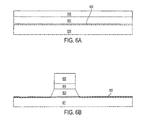
- FIGS. 6A-6C illustrate a manufacturing process for fabricating a gate with self-aligned ledges in accordance with an exemplary embodiment of the present invention.
- the base structure of the device is first formed with a base layer 601 of gallium nitride (GaN), a barrier layer 602 of aluminum gallium nitride (AlGaN) formed on the GaN layer 601 , and a layer of p-type gate material 603 formed on the barrier layer 602 , over which the gate metal 604 is deposited.
- GaN gallium nitride
- AlGaN aluminum gallium nitride
- a photoresist 605 is deposited and the gate metal 604 is then etched.
- the p-type gate material 603 is also etched in a manner that results in the gate structure depicted in FIG. 6B .
- the gate metal 604 is then etched isotropically, which results in the gate metal have a width less than the planar upper surface of the p-type gate material 603 . This second etching step results in the formation of the ledges 506 of the p-type gate material 603 .
- the manufacturing process includes a step of removing the photoresist 605 , which is not shown, and results in the gate with self-aligned ledge shown in FIG. 5 .
- contact metals for the drain and source contacts can be separately deposited using conventional fabrication techniques, but their formation will not be described herein so as to not unnecessarily obscure the aspects of the invention.
- FIGS. 7A-7B illustrate, respectively, a transmission electron microscopy (“TEM”) image of a cross-sectional view of a conventional transistor gate and an x ray of a cross-sectional view of a gate with a self-aligned ledge according to the exemplary embodiment disclosed herein.
- FIG. 8 illustrates a graph comparing the gate leakage current of the present invention (shown in FIG. 7B ) with the gate leakage current of a conventional transistor (shown in FIG. 7A ).
- the gate with self-aligned ledges has significantly lower gate leakage current than conventional gates without ledges when the transistor device is in the ON state.
- FIGS. 6A-6C are vastly superior to forming gate ledges using separate masks.
- a photoresist mask is applied to the unetched structure after the p-type gate material is deposited on the barrier layer of the device.
- the first mask is used to pattern and etch the gate metal to a minimum CD.
- a second mask is then used to pattern and etch the p-type material with a wider CD than the gate metal.
- One significant disadvantage of this two mask process is the possibility of misalignment between the gate metal and the p-type gate material.
Landscapes
- Junction Field-Effect Transistors (AREA)
- Electrodes Of Semiconductors (AREA)
- Thin Film Transistor (AREA)
Abstract
Description
Claims (7)
Priority Applications (1)
| Application Number | Priority Date | Filing Date | Title |
|---|---|---|---|
| US15/655,438 US10312335B2 (en) | 2009-04-08 | 2017-07-20 | Gate with self-aligned ledge for enhancement mode GaN transistors |
Applications Claiming Priority (6)
| Application Number | Priority Date | Filing Date | Title |
|---|---|---|---|
| US16777709P | 2009-04-08 | 2009-04-08 | |
| US12/756,960 US8404508B2 (en) | 2009-04-08 | 2010-04-08 | Enhancement mode GaN HEMT device and method for fabricating the same |
| US13/838,792 US8890168B2 (en) | 2009-04-08 | 2013-03-15 | Enhancement mode GaN HEMT device |
| US201361860976P | 2013-08-01 | 2013-08-01 | |
| US14/447,069 US9748347B2 (en) | 2009-04-08 | 2014-07-30 | Gate with self-aligned ledged for enhancement mode GaN transistors |
| US15/655,438 US10312335B2 (en) | 2009-04-08 | 2017-07-20 | Gate with self-aligned ledge for enhancement mode GaN transistors |
Related Parent Applications (1)
| Application Number | Title | Priority Date | Filing Date |
|---|---|---|---|
| US14/447,069 Division US9748347B2 (en) | 2009-04-08 | 2014-07-30 | Gate with self-aligned ledged for enhancement mode GaN transistors |
Publications (2)
| Publication Number | Publication Date |
|---|---|
| US20170317179A1 US20170317179A1 (en) | 2017-11-02 |
| US10312335B2 true US10312335B2 (en) | 2019-06-04 |
Family
ID=52432563
Family Applications (2)
| Application Number | Title | Priority Date | Filing Date |
|---|---|---|---|
| US14/447,069 Active 2030-06-11 US9748347B2 (en) | 2009-04-08 | 2014-07-30 | Gate with self-aligned ledged for enhancement mode GaN transistors |
| US15/655,438 Active US10312335B2 (en) | 2009-04-08 | 2017-07-20 | Gate with self-aligned ledge for enhancement mode GaN transistors |
Family Applications Before (1)
| Application Number | Title | Priority Date | Filing Date |
|---|---|---|---|
| US14/447,069 Active 2030-06-11 US9748347B2 (en) | 2009-04-08 | 2014-07-30 | Gate with self-aligned ledged for enhancement mode GaN transistors |
Country Status (7)
| Country | Link |
|---|---|
| US (2) | US9748347B2 (en) |
| JP (1) | JP2016529711A (en) |
| KR (1) | KR102193087B1 (en) |
| CN (1) | CN105453216A (en) |
| DE (1) | DE112014003495T5 (en) |
| TW (1) | TW201513341A (en) |
| WO (1) | WO2015017511A2 (en) |
Families Citing this family (22)
| Publication number | Priority date | Publication date | Assignee | Title |
|---|---|---|---|---|
| JP6222174B2 (en) | 2015-06-26 | 2017-11-01 | トヨタ自動車株式会社 | Nitride semiconductor device |
| US10401852B2 (en) * | 2015-11-04 | 2019-09-03 | Zoox, Inc. | Teleoperation system and method for trajectory modification of autonomous vehicles |
| US20180088749A1 (en) * | 2016-09-26 | 2018-03-29 | Uber Technologies, Inc. | Customized content generation for a user interface for a network service |
| US10339808B2 (en) * | 2017-04-03 | 2019-07-02 | Here Global B.V. | Predicting parking vacancies based on activity codes |
| KR102630424B1 (en) * | 2017-06-15 | 2024-01-29 | 이피션트 파워 컨버젼 코퍼레이션 | Enhancement-mode GaN transistor with selective and non-selective etch layers for improved uniformity of GaN spacer thickness |
| TWI680503B (en) | 2018-12-26 | 2019-12-21 | 杰力科技股份有限公司 | Method of manufacturing gate structure for gallium nitride hemt |
| TWI679770B (en) | 2018-12-26 | 2019-12-11 | 杰力科技股份有限公司 | Gallium nitride hemt and gate structure thereof |
| CN109817710A (en) * | 2018-12-29 | 2019-05-28 | 英诺赛科(珠海)科技有限公司 | High electron mobility transistor and its manufacturing method |
| CN109727863A (en) * | 2019-01-02 | 2019-05-07 | 北京大学深圳研究生院 | A kind of AlGan/GaN HEMT device structure and fabrication method based on self-alignment process |
| EP3686935A1 (en) * | 2019-01-23 | 2020-07-29 | IMEC vzw | Enhancement-mode high electron mobility transistor |
| US10818787B1 (en) | 2019-04-18 | 2020-10-27 | Semiconductor Components Industries, Llc | Electronic device including a high electron mobility transistor including a gate electrode and a dielectric film |
| CN117855265A (en) * | 2019-12-06 | 2024-04-09 | 联华电子股份有限公司 | High electron mobility transistor and method for manufacturing the same |
| KR102767849B1 (en) | 2019-12-12 | 2025-02-14 | 삼성전자주식회사 | Semiconductor device and method of fabricating the same |
| US12225738B2 (en) * | 2020-01-24 | 2025-02-11 | Rohm Co., Ltd. | Method for manufacturing nitride semiconductor device and nitride semiconductor device |
| US12046647B2 (en) | 2020-04-16 | 2024-07-23 | Innoscience (Zhuhai) Technology Co., Ltd. | Semiconductor device and fabrication method thereof |
| CN111682066A (en) * | 2020-06-19 | 2020-09-18 | 英诺赛科(珠海)科技有限公司 | Semiconductor device with improved gate leakage current |
| EP4012782A1 (en) | 2020-12-08 | 2022-06-15 | Imec VZW | Method of manufacturing a iii-n enhancement mode hemt device |
| CN115148793A (en) | 2021-03-30 | 2022-10-04 | 三星电子株式会社 | Power semiconductor device and method for manufacturing the same |
| CN114080691B (en) * | 2021-09-28 | 2024-06-21 | 英诺赛科(苏州)科技有限公司 | Nitride-based semiconductor device and method for manufacturing the same |
| TW202404087A (en) * | 2022-06-30 | 2024-01-16 | 聯華電子股份有限公司 | Method for manufacturing high electron mobility transistor device |
| TWI842078B (en) * | 2022-09-02 | 2024-05-11 | 力晶積成電子製造股份有限公司 | High electron mobility transistor device and manufacturing method thereof |
| KR20240047218A (en) * | 2022-10-04 | 2024-04-12 | 삼성전자주식회사 | Semiconductor device and method of manufacturing the same |
Citations (12)
| Publication number | Priority date | Publication date | Assignee | Title |
|---|---|---|---|---|
| US6730552B1 (en) | 2003-06-26 | 2004-05-04 | International Business Machines Corporation | MOSFET with decoupled halo before extension |
| US20040119110A1 (en) * | 2002-12-20 | 2004-06-24 | Samsung Electronics Co., Inc. | Non-volatile memory cells having floating gate and method of forming the same |
| US20060157735A1 (en) * | 2005-01-14 | 2006-07-20 | Fujitsu Limited | Compound semiconductor device |
| US20060273347A1 (en) * | 2005-06-06 | 2006-12-07 | Masahiro Hikita | Field-effect transistor and method for fabricating the same |
| US20090004872A1 (en) | 2001-11-07 | 2009-01-01 | Semiconductor Energy Laboratory Co., Ltd. | Method of manufacturing a semiconductor device |
| US20090072272A1 (en) * | 2007-09-17 | 2009-03-19 | Transphorm Inc. | Enhancement mode gallium nitride power devices |
| US20100258843A1 (en) * | 2009-04-08 | 2010-10-14 | Alexander Lidow | ENHANCEMENT MODE GaN HEMT DEVICE AND METHOD FOR FABRICATING THE SAME |
| US7939880B2 (en) | 2008-04-15 | 2011-05-10 | Freescale Semiconductor, Inc. | Split gate non-volatile memory cell |
| JP2011142182A (en) | 2010-01-06 | 2011-07-21 | Sharp Corp | Field-effect transistor |
| TW201232779A (en) | 2011-01-31 | 2012-08-01 | Taiwan Semiconductor Mfg | Enhancement-mode transistor and fabrication method thereof |
| TW201314898A (en) | 2011-09-28 | 2013-04-01 | 富士通股份有限公司 | Semiconductor device and manufacturing method |
| US20130168743A1 (en) | 2011-12-30 | 2013-07-04 | Stmicroelectronics, Inc. | Strained transistor structure |
-
2014
- 2014-07-29 TW TW103125846A patent/TW201513341A/en unknown
- 2014-07-30 KR KR1020167005532A patent/KR102193087B1/en active Active
- 2014-07-30 US US14/447,069 patent/US9748347B2/en active Active
- 2014-07-30 JP JP2016531852A patent/JP2016529711A/en active Pending
- 2014-07-30 CN CN201480043092.XA patent/CN105453216A/en active Pending
- 2014-07-30 DE DE112014003495.9T patent/DE112014003495T5/en not_active Withdrawn
- 2014-07-30 WO PCT/US2014/048826 patent/WO2015017511A2/en not_active Ceased
-
2017
- 2017-07-20 US US15/655,438 patent/US10312335B2/en active Active
Patent Citations (12)
| Publication number | Priority date | Publication date | Assignee | Title |
|---|---|---|---|---|
| US20090004872A1 (en) | 2001-11-07 | 2009-01-01 | Semiconductor Energy Laboratory Co., Ltd. | Method of manufacturing a semiconductor device |
| US20040119110A1 (en) * | 2002-12-20 | 2004-06-24 | Samsung Electronics Co., Inc. | Non-volatile memory cells having floating gate and method of forming the same |
| US6730552B1 (en) | 2003-06-26 | 2004-05-04 | International Business Machines Corporation | MOSFET with decoupled halo before extension |
| US20060157735A1 (en) * | 2005-01-14 | 2006-07-20 | Fujitsu Limited | Compound semiconductor device |
| US20060273347A1 (en) * | 2005-06-06 | 2006-12-07 | Masahiro Hikita | Field-effect transistor and method for fabricating the same |
| US20090072272A1 (en) * | 2007-09-17 | 2009-03-19 | Transphorm Inc. | Enhancement mode gallium nitride power devices |
| US7939880B2 (en) | 2008-04-15 | 2011-05-10 | Freescale Semiconductor, Inc. | Split gate non-volatile memory cell |
| US20100258843A1 (en) * | 2009-04-08 | 2010-10-14 | Alexander Lidow | ENHANCEMENT MODE GaN HEMT DEVICE AND METHOD FOR FABRICATING THE SAME |
| JP2011142182A (en) | 2010-01-06 | 2011-07-21 | Sharp Corp | Field-effect transistor |
| TW201232779A (en) | 2011-01-31 | 2012-08-01 | Taiwan Semiconductor Mfg | Enhancement-mode transistor and fabrication method thereof |
| TW201314898A (en) | 2011-09-28 | 2013-04-01 | 富士通股份有限公司 | Semiconductor device and manufacturing method |
| US20130168743A1 (en) | 2011-12-30 | 2013-07-04 | Stmicroelectronics, Inc. | Strained transistor structure |
Also Published As
| Publication number | Publication date |
|---|---|
| WO2015017511A3 (en) | 2015-11-05 |
| JP2016529711A (en) | 2016-09-23 |
| TW201513341A (en) | 2015-04-01 |
| US20170317179A1 (en) | 2017-11-02 |
| KR20160039671A (en) | 2016-04-11 |
| KR102193087B1 (en) | 2020-12-21 |
| CN105453216A (en) | 2016-03-30 |
| WO2015017511A2 (en) | 2015-02-05 |
| US20160035847A1 (en) | 2016-02-04 |
| US9748347B2 (en) | 2017-08-29 |
| DE112014003495T5 (en) | 2016-04-14 |
| US20170047414A9 (en) | 2017-02-16 |
Similar Documents
| Publication | Publication Date | Title |
|---|---|---|
| US10312335B2 (en) | Gate with self-aligned ledge for enhancement mode GaN transistors | |
| JP6434625B2 (en) | Oblique field plate power device and method of manufacturing oblique field plate power device | |
| JP6393758B2 (en) | GaN device with reduced output capacitance and process for making the same | |
| US8878246B2 (en) | High electron mobility transistors and methods of fabricating the same | |
| JP6051168B2 (en) | Manufacturing method of GaN transistor | |
| US9583480B2 (en) | Integrated circuit with matching threshold voltages and method for making same | |
| US9171911B2 (en) | Isolation structure in gallium nitride devices and integrated circuits | |
| US9214528B2 (en) | Method to fabricate self-aligned isolation in gallium nitride devices and integrated circuits | |
| JP2012134345A (en) | Semiconductor device and method of manufacturing the same | |
| CN109727918B (en) | Structure of integrated enhancement mode and depletion mode field effect transistor and manufacturing method thereof | |
| US20240282827A1 (en) | Field plate biasing of high electron mobility transistor |
Legal Events
| Date | Code | Title | Description |
|---|---|---|---|
| STPP | Information on status: patent application and granting procedure in general |
Free format text: NOTICE OF ALLOWANCE MAILED -- APPLICATION RECEIVED IN OFFICE OF PUBLICATIONS |
|
| STPP | Information on status: patent application and granting procedure in general |
Free format text: PUBLICATIONS -- ISSUE FEE PAYMENT VERIFIED |
|
| STCF | Information on status: patent grant |
Free format text: PATENTED CASE |
|
| MAFP | Maintenance fee payment |
Free format text: PAYMENT OF MAINTENANCE FEE, 4TH YR, SMALL ENTITY (ORIGINAL EVENT CODE: M2551); ENTITY STATUS OF PATENT OWNER: SMALL ENTITY Year of fee payment: 4 |
|
| IPR | Aia trial proceeding filed before the patent and appeal board: inter partes review |
Free format text: TRIAL NO: IPR2023-01384 Opponent name: INNOSCIENCE (ZHUHAI) TECHNOLOGY COMPANY, LTD., INNOSCIENCE AMERICA, INC., AND INNOSCIENCE (SHUZOU) TECHNOLOGY COMPANY, LTD. Effective date: 20230919 |
|
| RR | Request for reexamination filed |
Effective date: 20231013 |
|
| IPRC | Trial and appeal board: inter partes review certificate |
Kind code of ref document: K1 Free format text: INTER PARTES REVIEW CERTIFICATE; TRIAL NO. IPR2023-01384, SEP. 19, 2023 INTER PARTES REVIEW CERTIFICATE FOR PATENT 10,312,335, ISSUED JUN. 4, 2019, APPL. NO. 15/655,438, JUL. 20, 2017 INTER PARTES REVIEW CERTIFICATE ISSUED JUL. 8, 2025 Effective date: 20250708 |