US10298111B2 - PWM controller, switched-mode power supply, image forming apparatus, and PWM control method - Google Patents
PWM controller, switched-mode power supply, image forming apparatus, and PWM control method Download PDFInfo
- Publication number
- US10298111B2 US10298111B2 US15/996,662 US201815996662A US10298111B2 US 10298111 B2 US10298111 B2 US 10298111B2 US 201815996662 A US201815996662 A US 201815996662A US 10298111 B2 US10298111 B2 US 10298111B2
- Authority
- US
- United States
- Prior art keywords
- signal
- triangular wave
- carrier signal
- phase angle
- wave carrier
- Prior art date
- Legal status (The legal status is an assumption and is not a legal conclusion. Google has not performed a legal analysis and makes no representation as to the accuracy of the status listed.)
- Active
Links
- 238000000034 method Methods 0.000 title claims description 30
- 239000003990 capacitor Substances 0.000 claims description 18
- 230000000052 comparative effect Effects 0.000 description 16
- 238000010586 diagram Methods 0.000 description 14
- 230000008569 process Effects 0.000 description 12
- 230000000737 periodic effect Effects 0.000 description 4
- 230000008859 change Effects 0.000 description 3
- 230000003247 decreasing effect Effects 0.000 description 3
- 230000006870 function Effects 0.000 description 3
- 230000002159 abnormal effect Effects 0.000 description 2
- 230000003287 optical effect Effects 0.000 description 2
- 230000000694 effects Effects 0.000 description 1
- 238000012986 modification Methods 0.000 description 1
- 230000004048 modification Effects 0.000 description 1
Images


Classifications
-
- H—ELECTRICITY
- H02—GENERATION; CONVERSION OR DISTRIBUTION OF ELECTRIC POWER
- H02M—APPARATUS FOR CONVERSION BETWEEN AC AND AC, BETWEEN AC AND DC, OR BETWEEN DC AND DC, AND FOR USE WITH MAINS OR SIMILAR POWER SUPPLY SYSTEMS; CONVERSION OF DC OR AC INPUT POWER INTO SURGE OUTPUT POWER; CONTROL OR REGULATION THEREOF
- H02M1/00—Details of apparatus for conversion
- H02M1/08—Circuits specially adapted for the generation of control voltages for semiconductor devices incorporated in static converters
-
- G—PHYSICS
- G03—PHOTOGRAPHY; CINEMATOGRAPHY; ANALOGOUS TECHNIQUES USING WAVES OTHER THAN OPTICAL WAVES; ELECTROGRAPHY; HOLOGRAPHY
- G03G—ELECTROGRAPHY; ELECTROPHOTOGRAPHY; MAGNETOGRAPHY
- G03G15/00—Apparatus for electrographic processes using a charge pattern
- G03G15/50—Machine control of apparatus for electrographic processes using a charge pattern, e.g. regulating differents parts of the machine, multimode copiers, microprocessor control
- G03G15/5004—Power supply control, e.g. power-saving mode, automatic power turn-off
-
- G—PHYSICS
- G03—PHOTOGRAPHY; CINEMATOGRAPHY; ANALOGOUS TECHNIQUES USING WAVES OTHER THAN OPTICAL WAVES; ELECTROGRAPHY; HOLOGRAPHY
- G03G—ELECTROGRAPHY; ELECTROPHOTOGRAPHY; MAGNETOGRAPHY
- G03G15/00—Apparatus for electrographic processes using a charge pattern
- G03G15/80—Details relating to power supplies, circuits boards, electrical connections
-
- H—ELECTRICITY
- H02—GENERATION; CONVERSION OR DISTRIBUTION OF ELECTRIC POWER
- H02M—APPARATUS FOR CONVERSION BETWEEN AC AND AC, BETWEEN AC AND DC, OR BETWEEN DC AND DC, AND FOR USE WITH MAINS OR SIMILAR POWER SUPPLY SYSTEMS; CONVERSION OF DC OR AC INPUT POWER INTO SURGE OUTPUT POWER; CONTROL OR REGULATION THEREOF
- H02M3/00—Conversion of DC power input into DC power output
- H02M3/02—Conversion of DC power input into DC power output without intermediate conversion into AC
- H02M3/04—Conversion of DC power input into DC power output without intermediate conversion into AC by static converters
- H02M3/10—Conversion of DC power input into DC power output without intermediate conversion into AC by static converters using discharge tubes with control electrode or semiconductor devices with control electrode
- H02M3/145—Conversion of DC power input into DC power output without intermediate conversion into AC by static converters using discharge tubes with control electrode or semiconductor devices with control electrode using devices of a triode or transistor type requiring continuous application of a control signal
- H02M3/155—Conversion of DC power input into DC power output without intermediate conversion into AC by static converters using discharge tubes with control electrode or semiconductor devices with control electrode using devices of a triode or transistor type requiring continuous application of a control signal using semiconductor devices only
- H02M3/156—Conversion of DC power input into DC power output without intermediate conversion into AC by static converters using discharge tubes with control electrode or semiconductor devices with control electrode using devices of a triode or transistor type requiring continuous application of a control signal using semiconductor devices only with automatic control of output voltage or current, e.g. switching regulators
- H02M3/158—Conversion of DC power input into DC power output without intermediate conversion into AC by static converters using discharge tubes with control electrode or semiconductor devices with control electrode using devices of a triode or transistor type requiring continuous application of a control signal using semiconductor devices only with automatic control of output voltage or current, e.g. switching regulators including plural semiconductor devices as final control devices for a single load
-
- H—ELECTRICITY
- H02—GENERATION; CONVERSION OR DISTRIBUTION OF ELECTRIC POWER
- H02M—APPARATUS FOR CONVERSION BETWEEN AC AND AC, BETWEEN AC AND DC, OR BETWEEN DC AND DC, AND FOR USE WITH MAINS OR SIMILAR POWER SUPPLY SYSTEMS; CONVERSION OF DC OR AC INPUT POWER INTO SURGE OUTPUT POWER; CONTROL OR REGULATION THEREOF
- H02M7/00—Conversion of AC power input into DC power output; Conversion of DC power input into AC power output
- H02M7/42—Conversion of DC power input into AC power output without possibility of reversal
- H02M7/44—Conversion of DC power input into AC power output without possibility of reversal by static converters
- H02M7/48—Conversion of DC power input into AC power output without possibility of reversal by static converters using discharge tubes with control electrode or semiconductor devices with control electrode
- H02M7/53—Conversion of DC power input into AC power output without possibility of reversal by static converters using discharge tubes with control electrode or semiconductor devices with control electrode using devices of a triode or transistor type requiring continuous application of a control signal
- H02M7/537—Conversion of DC power input into AC power output without possibility of reversal by static converters using discharge tubes with control electrode or semiconductor devices with control electrode using devices of a triode or transistor type requiring continuous application of a control signal using semiconductor devices only, e.g. single switched pulse inverters
-
- H—ELECTRICITY
- H03—ELECTRONIC CIRCUITRY
- H03K—PULSE TECHNIQUE
- H03K4/00—Generating pulses having essentially a finite slope or stepped portions
- H03K4/06—Generating pulses having essentially a finite slope or stepped portions having triangular shape
-
- H—ELECTRICITY
- H03—ELECTRONIC CIRCUITRY
- H03K—PULSE TECHNIQUE
- H03K7/00—Modulating pulses with a continuously-variable modulating signal
- H03K7/08—Duration or width modulation ; Duty cycle modulation
Definitions
- Embodiments of the present disclosure relate to a pulse width modulation (PWM) controller, a switched-mode power supply, an image forming apparatus, and a PWM control method.
- PWM pulse width modulation
- an image forming apparatus generates a high voltage by using a switched-mode power supply including a PWM controller and a power converter.
- the PWM controller includes a sine wave calculator to generate a sine wave signal according to a frequency command value, a counter to generate a triangular wave carrier signal, and a comparator that compares the sine wave signal and the triangular wave carrier signal to generate and supply a PWM signal to the power converter.
- an improved PWM controller includes a sine wave calculator to generate a sine wave signal according to a frequency command value, a first counter to generate a first triangular wave carrier signal, and a comparator to compare the sine wave signal with the first triangular wave carrier signal, generate a PWM signal, and supply the PWM signal to a power converter.
- the PWM controller further includes a second counter to generate a second triangular wave carrier signal that is ⁇ rad behind the first triangular wave carrier signal and a carrier number calculator to calculate a carrier number based on a multiplication number.
- the carrier number indicates the number of carrier signals of the first triangular wave generated in a period in which a phase angle of the sine wave signal ranges from 0 to ⁇ /2 rad or from 0 to 3 ⁇ /2 rad, and the multiplication number is a ratio of a frequency of the first triangular wave carrier signal to the frequency command value.
- the PWM controller yet further includes a carrier control unit to switch a triangular wave carrier signal to the first triangular wave carrier signal or the second triangular wave carrier signal based on the carrier number, to supply the triangular wave carrier signal to the comparator in a first range of the phase angle ranging from 0 to ⁇ rad or a second range of the phase angle ranging from ⁇ to 2 ⁇ rad.
- FIG. 1 is a schematic view of an image forming apparatus according to an embodiment of the present disclosure
- FIG. 2 is a schematic block diagram illustrating a relation between a charging roller and a high-voltage power supply for charging as a switched-mode power supply according to an embodiment of the present disclosure
- FIG. 3 is a circuit diagram of the configuration of a high-voltage power supply as a comparative switched-mode power supply
- FIG. 4 is a block diagram of a comparative PWM controller in FIG. 3 ;
- FIG. 5 is a timing chart illustrating an example of a phase relation between a carrier signal and a modulated wave when voltage distortion occurs in a positive peak portion in the comparative PWM controller in FIG. 4 ;
- FIG. 6 is a timing chart illustrating an example of the phase relation between the carrier signal and the modulated wave when voltage distortion occurs in a negative peak portion in the comparative PWM controller in FIG. 4 ;
- FIG. 7 is a timing chart illustrating an example of the phase relation between the carrier signal and the modulated wave when distortion occurs in both the positive peak portion and negative peak portion in the comparative PWM controller in FIG. 4 ;
- FIG. 8 is a block diagram of a PWM controller of an image forming apparatus according to a first embodiment of the present disclosure
- FIG. 9 is a flowchart illustrating operations performed by the PWM controller of the image forming apparatus according to the first embodiment
- FIGS. 10A and 10B are sequence diagrams illustrating operations of a counter A and a counter B illustrated in FIG. 8 ;
- FIG. 11 is a circuit diagram of a specific example of the switching unit illustrated in FIG. 8 ;
- FIG. 12A is a flowchart of a carrier number calculation subroutine performed by a carrier number calculator illustrated in FIG. 8 ;
- FIG. 12B is a flowchart of a selection command generation subroutine performed by a selection command generator illustrated in FIG. 8 ;
- FIG. 13 is a flowchart of a carrier phase control subroutine performed by a phase control unit illustrated in FIG. 8 ;
- FIG. 14 is a timing chart illustrating an example of the phase relation between the carrier signal and the modulated wave when voltage distortion is eliminated in the positive peak portion by the PWM controller according to the first embodiment
- FIG. 15 is a timing chart illustrating an example of the phase relation between the carrier signal and the modulated wave when voltage distortion is eliminated in the negative peak portion by the PWM controller according to the first embodiment
- FIG. 16 is a table illustrating a relation between voltage distortion and the calculated result generated by the carrier number calculator illustrated in FIG. 8 ;
- FIG. 17 is a table illustrating the processed result generated by a selection command generator illustrated in FIG. 8 ;
- FIG. 18 is a table illustrating the processed result generated by a phase control unit illustrated in FIG. 8 ;
- FIG. 19 is a circuit diagram of a switched-mode power supply according to a second embodiment of the present disclosure.
- FIG. 1 is a schematic view of the image forming apparatus 1 according to a first embodiment of the present disclosure.
- an auto document feeder (ADF) 2 sequentially feeds a bundle of documents to an image reader 3 sheet by sheet, and the image reader 3 reads image data from each document.
- the image data read from the bundle of documents is converted to optical information by a writing unit 4 , and a photoconductor 6 uniformly charged by a charger is exposed based on the optical information from the writing unit 4 , thereby forming an electrostatic latent image.
- the developing device 7 develops the electrostatic latent image on the photoconductor 6 into a toner image.
- the toner image is then transferred onto a recording medium conveyed by a conveyance belt 8 and fixed thereon by a fixing device 9 .
- the recording medium bearing the toner image is output from the image forming apparatus 1 .
- FIG. 2 is a schematic block diagram illustrating a relation between a charging roller 11 and a high-voltage power supply for charging 20 serving as a switched-mode power supply.
- a command value generator 15 outputs a voltage command and a frequency command, which are output control signals, to the high-voltage power supply for charging 20 , and accepts an output current feedback (FB) signal output from the high-voltage power supply for charging 20 .
- FB output current feedback
- the high-voltage power supply for charging 20 generates and outputs a high voltage and a current to the charging roller 11 based on the voltage command and the frequency command input from the command value generator 15 and outputs the output current FB signal to the command value generator 15 .
- the charging roller 11 applies the high voltage and the current generated by the high-voltage power supply for charging 20 to the photoconductor 6 disposed opposite the charging roller 11 (the charger).
- FIG. 3 is a circuit diagram of the high-voltage power supply for charging 20 as a comparative switched-mode power supply.
- a power converter 31 A includes a pair of switching elements (transistors) Q 1 and Q 2 and a filter circuit 34 including a capacitor C 2 for removing a direct current (DC) component between the pair of switching elements Q 1 and Q 2 and a primary coil M 1 of a transformer 36 .
- the PWM controller 30 A includes a central processing unit (CPU) 30 Aa, a read only memory (ROM) 30 Ab, a random access memory (RAM) 30 Ac, and an analog to digital converter (ADC) 30 Ad.
- CPU central processing unit
- ROM read only memory
- RAM random access memory
- ADC analog to digital converter
- the CPU 30 Aa reads an operating system (OS) from the ROM 30 Ab, expands the OS on the RAM 30 Ac, and boots up the OS. Then, under the management of the OS, the CPU reads a program (a processing module) of the application software from the ROM 30 Ab and executes various processes.
- OS operating system
- a program a processing module
- the PWM controller 30 A may execute various types of processes using hardware such as a field-programmable gate array (FPGA) or the like, instead of software.
- FPGA field-programmable gate array
- the PWM controller 30 A accepts the frequency command and the voltage command from the command value generator 15 and the output current FB signal from the high-voltage power supply for charging 20 , performs PWM control, and outputs the PWM signal to the power converter 31 A.
- the power converter 31 A inputs the PWM signal supplied from the PWM controller 30 A to a half bridge circuit 32 , filters the signal in a sinusoidal manner by the filter circuit 34 , removes DC components by the capacitor C 2 for removing DC component, boosts the signal to the high voltage by the transformer 36 , and outputs the sinusoidal high voltage.
- the filter circuit 34 including the capacitor C 2 for removing DC component minimizes the periodic fluctuation of the output sine wave voltage and equalizes the voltage of the positive peak portion with the voltage of the negative peak portion, thereby keeping the surface potential of the photoconductor 6 constant. Accordingly, DC components can be easily removed without special control.
- FIG. 4 is a block diagram of a comparative PWM controller 30 A.
- the comparative PWM controller 30 A includes a microcomputer including, for example, the CPU 30 Aa, the ROM 30 Ab, and the RAM 30 Ac.
- the comparative PWM controller 30 A includes a synchronization control unit 41 , a sine wave calculator 42 , a multiplier 43 , an adder 44 , a comparator 45 , an offset 46 , a first counter A 47 , a clock 48 , and a Vpp control calculator 51 as the processing modules.
- the synchronization control unit 41 calculates a multiplication number n that is an integer obtained by dividing the frequency fc by the frequency command value fs based on the frequency command value fs input from the command value generator 15 and the frequency fc of the carrier signal A of the first triangular wave input from the counter A 47 (the first counter). Then, the synchronization control unit 41 calculates an angular speed ⁇ from the multiplication number n as expressed in equations below, and supplies the angular speed ⁇ to the sine wave calculator 42 , thereby synchronizing the first triangular wave carrier signal with the sine wave signal A.
- the sine wave calculator 42 calculates a sine wave (sin ⁇ t) according to the angular speed ⁇ . As a result, it is possible to synchronize the carrier signal A output from the counter A 47 with the sine wave signal (sin ⁇ t) output from the sine wave calculator 42 .
- the Vpp control calculator 51 accepts the voltage command from the command value generator 15 and performs Vpp control based on data digitally converted from the output voltage FB data by the ADC 50 .
- the multiplier 43 multiplies the sine wave signal sin ⁇ t by Vpp control value, and the adder 44 adds the multiplied result to an output OFS from the offset 46 , thereby generating a modulated wave y expressed by the following.
- y Vpp ⁇ sin ⁇ t+OFS
- the counter A 47 counts pulses from the clock 48 , generates a triangular wave carrier signal (a carrier wave), and outputs the triangular wave carrier signal to the comparator 45 .
- the comparator 45 compares the modulated wave y with the triangular wave carrier signal, generates the PWM signal, and outputs the PWM signal to the transistor Q 1 .
- An inverter 49 inverts the PWM signal and outputs an inverted PWM signal to the transistor Q 2 .
- FIG. 5 is a timing chart illustrating an example (Case 1) of a phase relation between the carrier signal and the modulated wave when voltage distortion occurs in the positive peak portion in the comparative PWM controller 30 A illustrated in FIG. 4 .
- the comparator 45 compares the modulated wave y (Sig 1 ) with the triangular wave carrier signal (Sig 2 ), generates the PWM signal, and output a high (H)-side PWM signal (Sig 4 ) to the transistor Q 1 .
- the inverter 49 inverts the PWM signal and output a low (L)-side PWM signal (Sig 5 ) to the transistor Q 2 .
- the H-side PWM signal (Sig 4 ) in the positive peak portion is off in an interval t 1 , and an output voltage is decreased and distorted toward a decreasing direction.
- the L-side PWM signal (Sig 5 ) in the negative peak portion is on in an interval t 2 , and the output voltage is not distorted.
- FIG. 6 is a timing chart illustrating an example (Case 2) of the phase relation between the carrier signal and the modulated wave when voltage distortion occurs in the negative peak portion in the comparative PWM controller 30 A illustrated in FIG. 4 .
- the phase of the H-side PWM signal in the positive peak portion is on in the interval t 1 , and the output voltage is not distorted.
- the phase of the L-side PWM signal in the negative peak portion is off in the interval t 2 , and the output voltage is decreased and distorted toward an increasing direction.
- FIG. 7 is a timing chart illustrating an example (Case 3) of the phase relation between the carrier signal and the modulated wave when voltage distortion occurs in both the positive peak portion and the negative peak portion in the comparative PWM controller 30 A illustrated in FIG. 4 .
- the phase of the H-side PWM signal in the positive peak portion is on in the interval t 1
- the phase of the L-side PWM signal in the negative peak portion is on in an interval t 2 .
- FIG. 8 is a block diagram of a PWM controller 30 B used in the image forming apparatus 1 according to the first embodiment of the present disclosure.
- the comparative PWM controller 30 A illustrated in FIG. 3 is replaced by the PWM controller 30 B illustrated in FIG. 8 .
- the PWM controller 30 B includes the microcomputer including, for example, the CPU 30 Aa, the ROM 30 Ab, and the RAM 30 Ac.
- the PWM controller 30 B further includes a carrier number calculator 61 , a carrier control unit 62 , a counter B 65 , and a switching unit 66 as the processing modules.
- the carrier number calculator 61 calculates the multiplication number n that is the integer obtained by dividing the frequency fc of the first triangular wave carrier signal by the frequency command value fs.
- the carrier number calculator 61 calculates a carrier number k based on the multiplication number n that indicates a ratio of the frequency fc of the first triangular wave carrier signal to the frequency command value fs.
- the carrier number k indicates the number of carrier signals of the first triangular wave generated when a phase angle of the sine wave signal ranges from 0 to ⁇ /2 rad or from 0 to 3 ⁇ /2 rad.
- the carrier control unit 62 switches the triangular wave carrier signal to the first triangular wave carrier signal or the second triangular wave carrier signal.
- the triangular wave carrier signal is supplied to the comparator 45 in a first range of the phase angle in which the phase angle of the sine wave signal is from 0 to ⁇ rad or a second range of the phase angle in which the phase angle of the sine wave signal is from ⁇ to 2 ⁇ rad.
- the carrier control unit 62 includes a selection command generator 63 and a phase control unit 64 .
- the selection command generator 63 Based on the carrier number k, the selection command generator 63 generates at least one of a first selection command and a second selection command to avoid generation of voltage distortion in the positive peak portion or the negative peak portion of the sine wave voltage, which is generated by the power converter 31 A according the phase of the PWM signal.
- the first selection command specifies the triangular wave carrier signal supplied to the comparator 45 in the first range of the phase angle from 0 to ⁇ rad
- the second selection command specifies the triangular wave carrier signal supplied to the comparator 45 in the second range of the phase angle from ⁇ to 2 ⁇ rad.
- the selection command generator 63 includes a prediction unit 63 a to predict whether voltage distortion exists in the positive peak portion or the negative peak portion of the sine wave voltage generated by the power converter 31 A according to the phase of the PWM signal based on the carrier number k. In a case in which the prediction unit 63 a predicts that voltage distortion exists in the positive peak portion or the negative peak portion, the selection command generator 63 generates the first selection command or the second selection command to avoid generation of voltage distortion in the positive peak portion or the negative peak portion of the sine wave voltage, which is generated by the power converter 31 A according the phase of the PWM signal.
- the prediction unit 63 a predicts that voltage distortion exists in the positive peak portion of the sine wave voltage generated by the power converter 31 A according the phase of the PWM signal. In a case in which the first decimal place of the carrier number k is 5, the prediction unit 63 a predicts that voltage distortion exists in the negative peak portion of the sine wave voltage generated by the power converter 31 A according the phase of the PWM signal.
- the selection command generator 63 When the prediction unit 63 a predicts that voltage distortion exists in the positive peak portion, the selection command generator 63 generates the second selection command to supply the second triangular wave carrier signal to the comparator 45 in the first range of the phase angle from 0 to ⁇ rad and the first selection command to supply the first triangular wave carrier signal to the comparator 45 in the second range of the phase angle from ⁇ to 2 ⁇ rad.
- the selection command generator 63 when the prediction unit 63 a predicts that voltage distortion exists in the negative peak portion, the selection command generator 63 generates the first selection command to supply the first triangular wave carrier signal to the comparator 45 in the first range of the phase angle from 0 to ⁇ rad and the second selection command to supply the second triangular wave carrier signal to the comparator 45 in the second range of the phase angle from ⁇ rad to 2 ⁇ rad.
- phase control unit 64 In a case in which the phase angle of the sine wave signal is in the first range of the phase angle from 0 to ⁇ rad, the phase control unit 64 generates a selection signal according to the first selection command. In a case in which the phase angle of the sine wave signal is in the second range of the phase angle from ⁇ to 2 ⁇ rad, the phase control unit 64 generates the selection signal according to the second selection command.
- the counter B 65 counts pulses from the clock 48 and outputs a count value B to the switching unit 66 . It is to be noted that the phase angle of the count value B of the counter B 65 is it rad (180°) ahead of the phase angle of the count value A of the counter A 47 .
- the switching unit 66 accepts a command by the phase control unit 64 , switches the counter between the counter A 47 and the counter B 65 , and outputs the optimum triangular wave carrier signal to the comparator 45 to avoid a distortion phase (the phase in which voltage distortion exists in either the positive peak portion or the negative peak portion).
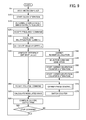
- FIG. 9 is a flowchart illustrating a control process from startup to normal operation of the PWM controller 30 B in the image forming apparatus 1 according to the first embodiment.
- step S 5 the PWM controller 30 B boots up a microcomputer.
- the CPU 30 Aa is reset, reads the operating system (OS) from the ROM 30 Ab, expands the OS on the RAM 30 Ac, and boots up the OS. Then, under the management of the OS, the CPU reads the program from the ROM 30 Ab and executes various processes. A basic clock is input to the CPU 30 Aa.
- OS operating system
- step S 10 the CPU 30 Aa starts a clock operation.
- the clock 48 outputs clock signals synchronizing with the basic clock.
- step S 15 the CPU 30 Aa determines a counter reset timing That is, the CPU 30 Aa sets a carrier frequency.
- step S 20 the CPU 30 Aa accepts the frequency command value fs as the output control signal from the command value generator 15 .
- steps S 35 and S 40 parallel processing is executed.
- step S 35 the CPU 30 Aa generates the reference sine-wave signal sin ⁇ t. That is, the sine wave calculator 42 calculates the sine-wave signal sin ⁇ t according to the angular speed ⁇ . As a result, it is possible to synchronize the carrier signal A output from the counter A 47 and the sine wave signal (sin ⁇ t) output from the sine wave calculator 42 .
- step S 40 the CPU 30 Aa calls a carrier number calculation subroutine illustrated in FIG. 12A .
- the carrier number calculator 61 calculates the multiplication number n that is the integer obtained by dividing the frequency fc of the first triangular wave carrier signal by the frequency command value fs.
- the carrier number calculator 61 calculates the carrier number k based on the multiplication number n that indicates the ratio of the frequency fc of the first triangular wave carrier signal to the frequency command value fs.
- the carrier number k indicates the number of carrier signals of the first triangular wave generated when the phase angle of the sine wave signal ranges from 0 to ⁇ /2 rad.
- the carrier number calculator 61 can calculate the carrier number k, which indicates the number of carrier signals of the first triangular wave generated when the phase angle of the sine wave signal ranges from 0 rad to 3 ⁇ /2 rad, based on the multiplication number n that indicates the ratio of the frequency fc of the first triangular wave carrier signal to the frequency command value fs.
- FIG. 12A is a flowchart of the carrier number calculation subroutine (S 40 ) illustrated in FIG. 8 .
- step S 110 processing of carrier number calculation is described in further detail below.
- the processing for cases (1) to (4) to be described later is executed in step S 110 in the flowchart illustrated in FIG. 12A .
- the command frequency is 100 Hz
- the command frequency is 111 Hz
- the command frequency is 105 Hz
- the command frequency is 117 Hz
- the carrier number calculator 61 calculates the carrier number k based on the multiplication number n (integral multiple) obtained by dividing the carrier frequency by the command frequency.
- FIG. 16 is a table illustrating a relation between voltage distortion and the calculated result generated by the carrier number calculator 61 illustrated in FIG. 8 .
- the command frequency, the carrier frequency, multiplication number n, the carrier number k, voltage distortion, and reference number of the drawing for each case are illustrated.
- step S 45 the CPU 30 Aa calls a selection command generation subroutine illustrated in FIG. 12B .
- the selection command generator 63 Based on the carrier number k, the selection command generator 63 generates at least one of the first selection command and the second selection command so that voltage distortion in the positive peak portion or the negative peak portion of the sine wave voltage, which is generated by the power converter 31 A according the phase of the PWM signal, is not generated.
- the first selection command specifies the triangular wave carrier signal supplied to the comparator 45 in the first range of the phase angle from 0 to ⁇ rad
- the second selection command specifies the triangular wave carrier signal supplied to the comparator 45 in the second range of the phase angle from ⁇ to 2 ⁇ rad.
- the selection command generator 63 includes the prediction unit 63 a to predict whether voltage distortion exists in the positive peak portion or the negative peak portion of the sine wave voltage generated by the power converter 31 A according the phase of the PWM signal based on the carrier number k. In a case in which the prediction unit 63 a predicts that voltage distortion exists in the positive peak portion or the negative peak portion, the selection command generator 63 generates the first selection command or the second selection command so that voltage distortion in the positive peak portion or the negative peak portion of the sine wave voltage, which is generated by the power converter 31 A according the phase of the PWM signal, is not generated.
- FIG. 12B is a flowchart of the selection command generation subroutine performed by the selection command generator 63 illustrated in FIG. 8 .
- the selection command generator 63 determines there is no need to switch the carrier phase in step S 170 . That is, the selection command generator 63 selects the carrier signal A generated by the counter A.
- step S 175 the selection command generator 63 set a flag to F 1 , and the process returns to main routine.
- the selection command generator 63 selects the selection command of the counter B 65 to select the carrier signal B generated by the counter B 65 in the period in which the sine wave signal is within 0° to 180° and selects the selection command of the counter A 47 to select the carrier signal A generated by the counter A 47 in the period in which the sine wave signal is within 180° to 360° in step S 180 .
- step S 185 the selection command generator 63 sets the flag to F 2 , and the process returns to the main routine.
- the selection command generator 63 selects the selection command of the counter A 47 to select the carrier signal A generated by the counter A 47 in the period in which the sine wave signal is within 0° to 180° and selects the selection command of the counter B 65 to select the carrier signal B generated by the counter B 65 in the period in which the sine wave signal is within 180° to 360° in step S 190 .
- step S 185 the selection command generator 63 set the flag to F 3 , and the process returns to the main routine.
- FIG. 17 is a table illustrating the processed result performed by the selection command generator 63 illustrated in FIG. 8 .
- the carrier number k, the selected counter in a case of no counter change, sine wave signal 0 to ⁇ rad (0° to 180°), or sine wave signal ⁇ to 2 ⁇ rad (180° to 360°), and the flag for each case are illustrated.
- the selection command generator 63 selects counter B 65 in the period from 0 to ⁇ rad (0° to 180°) and selects counter A 47 in the period from ⁇ to 2 ⁇ rad (180° to 360°).
- the selection command generator 63 selects counter A 47 in the period from 0 to ⁇ rad (0° to 180°) and selects counter B 65 in the period from ⁇ to 2 ⁇ rad (180° to 360°).
- step S 50 the CPU 30 Aa executes carrier generation (counter A operation).
- the counter A 47 counts pulses from the clock 48 , generates the triangular wave carrier signal (carrier wave), and outputs the carrier signal to the switching unit 66 .
- step S 55 the CPU 30 Aa executes carrier generation (counter B operation).
- the counter B 65 counts pulses from the clock 48 and outputs the count value B to the switching unit 66 .
- the phase angle of the count value B of the counter B 65 is ⁇ rad (180°) ahead of the phase angle of the count value A of the counter A 47 .
- steps S 60 and S 70 the parallel processing is executed.
- step S 60 the CPU 30 Aa accepts the voltage command as the output control signal from the command value generator 15 . That is, the Vpp control calculator 51 accepts the voltage command from the command value generator 15 , calculates the Vpp control value based on data digitally converted from the output voltage FB data by the ADC 50 , and supplies the Vpp control value to the multiplier 43 .
- step S 65 the CPU 30 Aa executes a modulated wave calculation.
- step S 70 the CPU 30 Aa calls a carrier phase control subroutine illustrated in FIG. 13 .
- phase control unit 64 In a case in which the phase angle of the sine wave signal is in the first range of the phase angle from 0 to ⁇ rad, the phase control unit 64 generates the selection signal according to the first selection command. In a case in which the phase angle of the sine wave signal is in the second range of the phase angle from ⁇ to 2 ⁇ rad, the phase control unit 64 generates the selection signal according to the second selection command.
- FIG. 13 is a flowchart of the carrier phase control subroutine performed by the phase control unit 64 illustrated in FIG. 8 .
- the phase control unit 64 monitors the phase of the angular speed (wt) of the sine wave signal and controls the counter switching performed by the switching unit 66 according to the counter selection command specified by the flag input from the selection command generator 63 .
- step S 210 the phase control unit 64 accepts the sine wave signal sin ⁇ t generated by the sine wave calculator 42 .
- step S 215 the phase control unit 64 determines whether the phase of the angular speed ( ⁇ t) of the sine wave signal sin ⁇ t is in the period from ⁇ to 2 ⁇ (i.e., from 180° to 360°).
- step S 225 if the phase of the angular speed ( ⁇ t) is in the period from ⁇ to 2 ⁇ , the process proceeds to step S 225 .
- the process proceeds to step S 220 .
- phase control unit 64 determines whether the phase control unit 64 has accepted the counter A selection command according to the flag input from the selection command generator 63 in step S 220 .
- phase control unit 64 determines whether the phase control unit 64 has accepted the counter A selection command according to the flag input from the selection command generator 63 in step S 225 .
- step S 230 the phase control unit 64 sets a switching signal s 0 (Sig 3 ) to 0 in order to select the carrier output from the counter A.
- step S 235 the phase control unit 64 sets the switching signal s 0 (Sig 3 ) to 1 in order to select the counter B.
- FIG. 18 is a table illustrating the processed result generated by the phase control unit 64 illustrated in FIG. 8 .
- the switching signals s 0 (Sig 3 ) of the sine wave signal (0° to 180°) and the sine wave signal (180° to 360°) for each flag are illustrated.
- the phase control unit 64 outputs the switching signal s 0 (Sig 3 ) to the switching unit 66 according to the range of the angular speed of the sine wave signal.
- the switching unit 66 accepts the carrier signal A from the counter A 47 and the carrier signal B from the counter B 65 together. Then, the switching unit 66 outputs the selected carrier signal to the comparator 45 according to the switching signal s 0 input from phase control unit 64 .
- step S 75 the CPU 30 Aa executes counter switching operation.
- the switching unit 66 accepts the command by the phase control unit 64 , switches between the counter A 47 and the counter B 65 , and output the optimum triangular wave carrier signal to the comparator 45 to avoid the distortion phase (the phase in which voltage distortion exists in the positive peak portion or the negative peak portion).
- step S 80 the CPU 30 Aa executes carrier comparison and PWM signal output operation. That is, the comparator 45 compares the modulated wave y with the triangular wave carrier signal, generates the PWM signal, and outputs the PWM signal to the transistor Q 1 .
- the inverter 49 inverts the PWM signal and outputs the inverted PWM signal to the transistor Q 2 .
- the power converter 31 A inputs the PWM signal supplied from the PWM controller 30 B to the half bridge circuit 32 and generates a power pulse signal including a sinusoidal envelop according to the PWM signal in the half bridge circuit 32 . Then, the power converter 31 A filters the power pulse signal in a sinusoidal manner by the filter circuit 34 , removes DC components by the capacitor C 2 for removing DC component, boosts the signal to a high voltage by the transformer 36 , and outputs a sinusoidal high voltage.
- step S 85 the CPU 30 Aa determines whether the CPU 30 Aa has accepted a stop command as the output control signal from the command value generator 15 . If the CPU 30 Aa has accepted the stop command, the process proceeds to step S 20 . On the other hand, if the CPU 30 Aa has not accepted the stop command, the process proceeds to steps S 60 and S 70 .
- FIGS. 10A and 10B are sequence diagrams illustrating operations of the counter A 47 and the counter B 65 illustrated in FIG. 8 .
- the phase difference between the counter A 47 and the counter B 65 is ⁇ rad (180°).
- the phase angle of the count value B (Sig 2 B) of the counter B 65 is ⁇ rad (180°) ahead of the phase angle of the count value A (Sig 2 A) of the counter A 47 .
- FIG. 11 is a circuit diagram of an example of the switching unit 66 illustrated in FIG. 8 .
- the switching unit 66 accepts the carrier signal A as an input data d 0 from the counter A 47 and the carrier signal B as input data dl from the counter B 65 .
- the switching unit 66 includes a multiplexer (MUX) to switch an output data to the input data d 0 or the input data dl according to the selection signal s 0 . If the selection signal s 0 (Sig 3 ) from the phase control unit 64 illustrated in FIG. 5 is 0, the switching unit 66 outputs the signal of the counter A 47 . Alternatively, if the selection signal s 0 (Sig 3 ) from the phase control unit 64 is 1, the switching unit 66 outputs the signal of the counter B 65 to the comparator 45 .
- MUX multiplexer
- FIG. 14 is a timing chart illustrating an example of the phase relation between the carrier signal and the modulated wave when voltage distortion is eliminated in the positive peak portion by the PWM controller 30 B.
- the command frequency is 100 Hz
- the surface potential of the photoconductor 6 can be kept constant, and abnormal images can be prevented.
- FIG. 15 is a timing chart illustrating an example of the phase relation between the carrier signal and the modulated wave when distortion is eliminated in the negative peak in the PWM controller 30 B.
- FIG. 15 voltage distortion in the negative peak portion is eliminated by performing the control illustrated in FIGS. 8 and 9 .
- the command frequency is 111 Hz
- the surface potential of the photoconductor 6 can be kept constant, and abnormal images, which are seen in the comparative embodiment, can be prevented.
- the triangular wave carrier signal is switched to the first triangular wave carrier signal (Sig 2 A) or the second triangular wave carrier signal (Sig 2 B).
- the carrier number k indicates the number of carrier signals of the first triangular wave (Sig 2 A) generated when the phase angle of the sine wave signal (Sig 1 ) is from 0 to ⁇ /2 rad or from 0 to 3 ⁇ /2 rad.
- the triangular wave carrier signal is supplied to the comparator 45 in the first range of the phase angle in which the phase angle of the sine wave signal (Sig 1 ) is from 0 to ⁇ rad, or the second range of the phase angle in which the phase angle of the sine wave signal (Sig 1 ) is from ⁇ to 2 ⁇ rad. Therefore, voltage distortion in the positive peak portion or the negative peak portion of the output sine wave (Sig 6 ) generated by the power converter 31 A can be minimized.
- FIG. 19 is a circuit diagram of a high-voltage power supply for charging as a switched-mode power supply according to a second embodiment of the present disclosure.
- the power converter 31 B includes a pair of capacitors C 12 and C 13 connected in series to both polarity terminals of the DC power supply.
- the pair of switching elements is a first transistor Q 1 and a second transistor Q 2 , a source terminal of the first transistor Q 1 is connected to positive polarity terminals of the DC power supply, drain terminals of the first transistor Q 1 and the second transistor Q 2 are connected to each other and further commonly connected to a terminal of a primary coil M 1 via a low pass filter 72 , and a source terminal of the second transistor Q 2 are connected to a common connection midpoint between the pair of the capacitors C 12 and C 13 , and further connected to the other terminal of the primary coil M 1 .
- the PWM controller 30 B accepts the frequency command and the voltage command from the command value generator 15 and the output current FB signal from the high-voltage power supply for charging 20 , performs PWM control, and outputs the PWM signal to the power converter 31 B.
- the power converter 31 B inputs the PWM signal supplied from the PWM controller 30 B to the half bridge circuit 32 , generates a midpoint potential at a connection point between the capacitors C 12 and C 13 of a midpoint generation capacitor 71 , and generates a power pulse signal including a sinusoidal envelop according to the PWM signal in the half bridge circuit 32 . Then, the power converter 31 B filters the power pulse signal in a sinusoidal manner by the low pass filter 72 , boosts the signal to the high voltage by the transformer 36 , and outputs the sinusoidal high voltage.
- the midpoint generation capacitor 71 minimizes the periodic fluctuation of the output sine wave voltage and equalizes the voltage of the positive peak portion with the voltage of the negative peak portion, thereby keeping the surface potential of the photoconductor 6 constant. Therefore, it is possible to control the DC component.
- a PWM controller 30 B includes a sine wave calculator 42 to generate a sine wave signal according to a frequency command value fs, a counter A 47 (a first counter) to generate a first triangular wave carrier signal, and a comparator 45 to compare the sine wave signal with the first triangular wave carrier signal, generate a PWM signal, and supply the PWM signal to a power converter 31 A.
- the PWM controller 30 B further includes a counter B 65 (a second counter) to generate a second triangular wave carrier signal that is ⁇ rad behind the first triangular wave carrier signal and a carrier number calculator 61 to calculate a carrier number k based on a multiplication number n.
- the carrier number k indicates the number of carrier signals of the first triangular wave generated in a period in which a phase angle of the sine wave signal ranges from 0 to ⁇ /2 rad or from 0 to 3 ⁇ /2 rad
- the multiplication number n indicates a ratio of a frequency fc of the first triangular wave carrier signal to the frequency command value fs.
- the PWM controller 30 B yet further includes a carrier control unit 62 to switch a triangular wave carrier signal to the first triangular wave carrier signal or the second triangular wave carrier signal based on the carrier number k, to supply the triangular wave carrier signal to the comparator 45 in a first range of the phase angle ranging from 0 to ⁇ rad or a second range of the phase angle ranging from ⁇ to 2 ⁇ rad.
- a carrier control unit 62 to switch a triangular wave carrier signal to the first triangular wave carrier signal or the second triangular wave carrier signal based on the carrier number k, to supply the triangular wave carrier signal to the comparator 45 in a first range of the phase angle ranging from 0 to ⁇ rad or a second range of the phase angle ranging from ⁇ to 2 ⁇ rad.
- the triangular wave carrier signal is switched to the first triangular wave carrier signal or the second triangular wave carrier signal.
- the triangular wave carrier signal is supplied to the comparator 45 in the first range of the phase angle in which the phase angle of the sine wave signal is from 0 to ⁇ rad, or the second range of the phase angle in which the phase angle of the sine wave signal is from ⁇ to 2 ⁇ rad. Therefore, a voltage distortion (a waveform distortion) in the positive peak portion or the negative peak portion of the output sine wave generated by the power converter 31 A can be minimized.
- the carrier control unit 62 includes a selection command generator 63 to generate at least one of a first selection command and a second selection command to avoid voltage distortion in the positive peak portion or the negative peak portion of the sine wave voltage generated by the power converter 31 A according to a phase of the PWM signal.
- the first selection command specifies the triangular wave carrier signal supplied to the comparator 45 in the first range of the phase angle
- the second selection command specifies the triangular wave carrier signal supplied to the comparator 45 in the second range of the phase angle.
- the carrier control unit 62 further includes a phase control unit 64 to generate a selection signal according to the first selection command when the phase angle of the sine wave signal is within the first range of the phase angle and to generate a selection signal according to the second selection command when the phase angle of the sine wave signal is within the second range of the phase angle.
- the selection command generator 63 generates at least one of the first selection command and the second selection command to avoid voltage distortion in the positive peak portion or the negative peak portion of the sine wave voltage generated by the power converter 31 A according to the phase of the PWM signal.
- the phase control unit 64 generates the selection signal according to the first selection command when the phase angle of the sine wave signal is within the first range of the phase angle and to generate the selection signal according to the second selection command when the phase angle of the sine wave signal is within the second range of the phase angle. Therefore, voltage distortion can be prevented in the positive peak portion or the negative peak portion of the sine wave voltage generated by the power converter 31 A according to the phase of the PWM signal.
- the selection command generator 63 includes a prediction unit 63 a to predict whether voltage distortion exists in the positive peak portion or the negative peak portion of the sine wave voltage generated by the power converter 31 A according to the phase of the PWM signal based on the carrier number k. In a case in which the prediction unit 63 a predicts that voltage distortion exists in the positive peak portion or the negative peak portion, the selection command generator 63 generates the first selection command or the second selection command so that voltage distortion in the positive peak portion or the negative peak portion of the sine wave voltage, which is generated by the power converter 31 A according the phase of the PWM signal, is not generated.
- the selection command generator 63 in a case in which the prediction unit 63 a predicts that voltage distortion exists in the positive peak portion or the negative peak portion, the selection command generator 63 generates the first selection command or the second selection command so that voltage distortion in the positive peak portion or the negative peak portion of the sine wave voltage, which is generated by the power converter 31 A according the phase of the PWM signal, is not generated. Therefore, voltage distortion can be prevented.
- the prediction unit 63 a predicts that voltage distortion exists in the positive peak of the sine wave voltage generated by the power converter 31 A according the phase of the PWM signal. In a case in which a first decimal place of the carrier number k is 5, the prediction unit 63 a predicts that voltage distortion exists in the negative peak portion of the sine wave voltage generated by the power converter 31 A according the phase of the PWM signal.
- the prediction unit 63 a can predict whether voltage distortion exists in the positive peak portion or the negative peak portion of the sine wave voltage generated by the power converter 31 A based on the carrier number k.
- the selection command generator 63 when the prediction unit 63 a predicts that voltage distortion exists in the positive peak portion, the selection command generator 63 generates the second selection command to supply the second triangular wave carrier signal to the comparator 45 in the first range of the phase angle and the first selection command to supply the first triangular wave carrier signal to the comparator 45 in the second range of the phase angle.
- the selection command generator 63 when the prediction unit 63 a predicts that voltage distortion exists in the negative peak portion, the selection command generator 63 generates the first selection command to supply the first triangular wave carrier signal to the comparator 45 in the first range of the phase angle and the second selection command to supply the second triangular wave carrier signal to the comparator 45 in the second range of the phase angle.
- the carrier number calculator 61 calculates multiplication number n that is an integer obtained by dividing the frequency fc of the first triangular wave carrier signal by the frequency command value fs.
- the CPU 30 Aa can generate the carrier signal fc of the first triangular wave that is a value obtained by multiplying the frequency command value fs by the multiplication number n.
- the PWM controller 30 B includes the synchronization control unit 41 that calculates the multiplication number n.
- the multiplication number n is obtained by dividing the frequency fc of the first triangular wave carrier signal by the frequency command value fs based on the frequency command value fs input from the command value generator 15 and the carrier signal fc of the first triangular wave input from the counter A 47 (the first counter).
- the synchronization control unit 41 calculates the angular speed w from the multiplication number n, and supplies the angular speed w to the sine wave calculator 42 , thereby synchronizing the first triangular wave carrier signal and the sine wave signal.
- a switched-mode power supply includes the PWM controller 30 B according to Aspect 1 and the power converter 31 to accept the PWM signal from the PWM controller 30 B.
- the power converter 31 includes a pair of switching elements Q 1 and Q 2 connected to a DC power supply to turn on and off alternately according to the PWM signal generated by the PWM controller 30 B and a transformer 36 including a primary coil M 1 to transform electric power to magnetic energy and a secondary coil M 2 .
- the electric power is supplied from the DC power supply by the pair of switching elements Q 1 and Q 2 turning on and off alternately.
- the secondary coil M 2 is coupled to the primary coil M 1 magnetically to induce magnetic energy.
- the output sine wave can be generated in which voltage distortion in the positive peak portion or the negative peak portion is minimized.
- the power converter 31 A illustrated in FIG. 3 includes a filter circuit 34 between the pair of switching elements Q 1 and Q 2 and the primary coil M 1 of a transformer 36 .
- the filter circuit 34 includes a capacitor C 2 for removing a DC component.
- the filter circuit 34 including the capacitor C 2 for removing DC component can minimize the periodic fluctuation of the output sine wave voltage and equalize the voltage of the positive peak portion with the voltage of the negative peak portion. As a result, it is possible to remove the DC component of the output sine wave voltage output from the power converter 31 A.
- the power converter 31 B illustrated in FIG. 19 includes a pair of capacitors C 12 and C 13 connected in series to both polarity terminals of the DC power supply.
- the pair of switching elements is a first transistor Q 1 and a second transistor Q 2 .
- a source terminal of the first transistor Q 1 is connected to positive polarity terminal of the DC power supply
- drain terminals of the first transistor Q 1 and the second transistor Q 2 are commonly connected to each other and further connected to a terminal of the primary coil M 1 via a low pass filter 72
- a source terminal of the second transistor Q 2 is connected to a common connection midpoint between the pair of capacitor C 12 and C 13 and further connected to the other terminal of the primary coil M 1 .
- the source terminal of the second transistor Q 2 is connected to the common connection midpoint between the pair of capacitor C 12 and C 13 , and further connected to the other terminal of the primary coil M 1 , it is possible to minimize the periodic fluctuation of the output sine wave voltage and equalize the voltage of the positive peak portion with the voltage of the negative peak portion. As a result, it is possible to control the DC component output from the power converter 31 B.
- an image forming apparatus 1 includes the switched-mode power supply according to Aspect 10, a charging roller 11 (a charger) coupled to the secondary coil M 2 of the transformer 36 , and a photoconductor 6 disposed opposite the charging roller 11 (the charger).
- the output sine wave voltage can be generated in which voltage distortion in the positive peak portion or the negative peak portion is minimized and applied to the photoconductor 6 via the charging roller 11 .
- the stable sine wave voltage can keep the surface potential of the photoconductor 6 constant.
- a method for performing PWM control includes generating a sine wave signal according to a frequency command value fs, generating a first triangular wave carrier signal, comparing the sine wave signal with the first triangular wave carrier signal, generating a PWM signal, and supplying the PWM signal to a power converter 31 .
- the method further includes generating a second triangular wave carrier signal that is n rad behind the first triangular wave carrier signal and calculating a carrier number k based on a multiplication number n.
- the carrier number k indicates the number of carrier signals of the first triangular wave generated in a period in which a phase angle of the sine wave signal ranges from 0 to ⁇ /2 rad or from 0 to 3 ⁇ /2 rad
- the multiplication number n indicates a ratio of a frequency fc of the first triangular wave carrier signal to the frequency command value fs.
- the method yet further includes switching a triangular wave carrier signal to the first triangular wave carrier signal or the second triangular wave carrier signal based on the carrier number k, to supply the triangular wave carrier signal to the comparator in a first range of the phase angle ranging from 0 to ⁇ rad or a second range of the phase angle ranging from ⁇ to 2 ⁇ rad.
- Aspect 14 The operation and effect according to Aspect 14 are the same or substantially the same as those of the Aspect 1. Therefore, redundant description is omitted below.
- a non-transitory recording medium storing a program which, when executed by one or more processors, cause the one or more processors to perform a method.
- the method includes generating a sine wave signal according to a frequency command value fs, generating a first triangular wave carrier signal, comparing the sine wave signal with the first triangular wave carrier signal, generating a PWM signal, and supplying the PWM signal to a power converter 31 .
- the method further includes generating a second triangular wave carrier signal that is ⁇ rad behind the first triangular wave carrier signal and calculating a carrier number k based on a multiplication number n.
- the carrier number k indicates the number of carrier signals of the first triangular wave generated in a period in which a phase angle of the sine wave signal ranges from 0 to ⁇ /2 rad or from 0 to 3 ⁇ /2 rad
- the multiplication number n indicates a ratio of a frequency fc of the first triangular wave carrier signal to the frequency command value fs.
- the method yet further includes switching a triangular wave carrier signal to the first triangular wave carrier signal or the second triangular wave carrier signal based on the carrier number k, to supply the triangular wave carrier signal to the comparator in a first range of the phase angle ranging from 0 to ⁇ rad or a second range of the phase angle ranging from ⁇ to 2 ⁇ rad.
- the processor can perform the method.
- Processing circuitry includes a programmed processor, as a processor includes circuitry.
- a processing circuit also includes devices such as an application specific integrated circuit (ASIC), digital signal processor (DSP), field programmable gate array (FPGA), and conventional circuit components arranged to perform the recited functions.
- ASIC application specific integrated circuit
- DSP digital signal processor
- FPGA field programmable gate array
Landscapes
- Engineering & Computer Science (AREA)
- Power Engineering (AREA)
- Physics & Mathematics (AREA)
- General Physics & Mathematics (AREA)
- Microelectronics & Electronic Packaging (AREA)
- Inverter Devices (AREA)
Abstract
Description
n=fc/fs
fs=fc/n(Hz)
ω=2πfs=2πfc/n(rad/s)
y=Vpp×sin ωt+OFS
n=fc/fs
fs=fc/n(Hz)
ω=2πfs=2πfc/n(rad/s)
k=20×(90°/360°)=5.00.
k=18×(90°/360°)=4.50.
k=19×(90°/360°)=4.75.
k=17×(90°/360°)=4.25.
y=Vpp×sin ωt+OFS
k=20×(90°/360°)=5.00.
k=18×(90°/360°)=4.50.
Claims (20)
Applications Claiming Priority (2)
| Application Number | Priority Date | Filing Date | Title |
|---|---|---|---|
| JP2017119478A JP2019004653A (en) | 2017-06-19 | 2017-06-19 | PWM control apparatus, switching power supply apparatus, image forming apparatus, PWM control method, and program |
| JP2017-119478 | 2017-06-19 |
Publications (2)
| Publication Number | Publication Date |
|---|---|
| US20180367021A1 US20180367021A1 (en) | 2018-12-20 |
| US10298111B2 true US10298111B2 (en) | 2019-05-21 |
Family
ID=64657719
Family Applications (1)
| Application Number | Title | Priority Date | Filing Date |
|---|---|---|---|
| US15/996,662 Active US10298111B2 (en) | 2017-06-19 | 2018-06-04 | PWM controller, switched-mode power supply, image forming apparatus, and PWM control method |
Country Status (2)
| Country | Link |
|---|---|
| US (1) | US10298111B2 (en) |
| JP (1) | JP2019004653A (en) |
Families Citing this family (8)
| Publication number | Priority date | Publication date | Assignee | Title |
|---|---|---|---|---|
| US10541602B2 (en) * | 2017-10-30 | 2020-01-21 | University Of Florida Research Foundation, Inc. | SPWM with DC offset based on total energy reduction |
| JP7159621B2 (en) | 2018-05-31 | 2022-10-25 | 株式会社リコー | VOLTAGE GENERATOR, POWER CONTROL DEVICE, IMAGE FORMING APPARATUS, AND CONTROL METHOD |
| JP7125655B2 (en) | 2019-01-15 | 2022-08-25 | トヨタ自動車株式会社 | negative electrode |
| JP2022091378A (en) * | 2020-12-09 | 2022-06-21 | 東京エレクトロン株式会社 | Power source and inspection device |
| CN113347746B (en) * | 2021-08-09 | 2021-11-26 | 深圳市微源半导体股份有限公司 | Heating wire drive circuit and electronic equipment |
| CN115811242A (en) * | 2021-09-15 | 2023-03-17 | 山特电子(深圳)有限公司 | Pulse width modulation method for cascaded H-bridge type power converter |
| JP7768003B2 (en) | 2022-03-23 | 2025-11-12 | 株式会社リコー | Power conversion device and image forming device |
| TWI903958B (en) * | 2024-12-30 | 2025-11-01 | 致茂電子股份有限公司 | High-resolution pwm signal generator based on fpga |
Citations (1)
| Publication number | Priority date | Publication date | Assignee | Title |
|---|---|---|---|---|
| JPH08251930A (en) | 1995-03-14 | 1996-09-27 | Hitachi Ltd | PWM controller and system using the same |
Family Cites Families (8)
| Publication number | Priority date | Publication date | Assignee | Title |
|---|---|---|---|---|
| JP2903444B2 (en) * | 1991-10-11 | 1999-06-07 | 株式会社電研 | PWM inverter device |
| US7148633B2 (en) * | 2004-10-18 | 2006-12-12 | Beyond Innovation Technology | DC/AC inverter |
| JP2008091306A (en) * | 2006-10-05 | 2008-04-17 | Sanken Electric Co Ltd | Frequency synchronizing method of discharge tube lighting device, discharge tube lighting device and semiconductor integrated circuit |
| JP2010035260A (en) * | 2008-07-25 | 2010-02-12 | Honda Motor Co Ltd | Inverter generator |
| JP2012055141A (en) * | 2010-09-03 | 2012-03-15 | Ricoh Co Ltd | Ac power supply device, charging device, and image forming device |
| CN104704735B (en) * | 2012-11-09 | 2017-09-26 | 富士电机株式会社 | Inverter unit |
| CN105075099B (en) * | 2013-10-08 | 2017-09-22 | 富士电机株式会社 | Power conversion device |
| KR101751001B1 (en) * | 2015-11-02 | 2017-06-26 | 전남대학교산학협력단 | Switch control device and method for elimination of the leakage current in three-level inverter by using carrier based pulse width modulation |
-
2017
- 2017-06-19 JP JP2017119478A patent/JP2019004653A/en active Pending
-
2018
- 2018-06-04 US US15/996,662 patent/US10298111B2/en active Active
Patent Citations (1)
| Publication number | Priority date | Publication date | Assignee | Title |
|---|---|---|---|---|
| JPH08251930A (en) | 1995-03-14 | 1996-09-27 | Hitachi Ltd | PWM controller and system using the same |
Also Published As
| Publication number | Publication date |
|---|---|
| US20180367021A1 (en) | 2018-12-20 |
| JP2019004653A (en) | 2019-01-10 |
Similar Documents
| Publication | Publication Date | Title |
|---|---|---|
| US10298111B2 (en) | PWM controller, switched-mode power supply, image forming apparatus, and PWM control method | |
| US8897042B2 (en) | Power source system and control circuit | |
| US9880485B2 (en) | Image forming apparatus | |
| EP3109709B1 (en) | Power supply unit and image forming apparatus | |
| US20150093137A1 (en) | High-voltage power source, charging device incorporating same, and high-voltage power supplying method | |
| JP4172235B2 (en) | Grid-connected inverter device | |
| US10591858B2 (en) | Voltage generation device, power control device, image forming apparatus, and control method | |
| US20130016990A1 (en) | Power supply apparatus and method of supplying power | |
| US10379457B2 (en) | Image forming apparatus | |
| KR101904101B1 (en) | Method for removing DC component of MMC converter output | |
| JP5742150B2 (en) | Synchronous control device for AC / DC converter | |
| US20140368187A1 (en) | Control circuit, and power generation device having the same | |
| JP2020188682A (en) | Non-contact power supply device and program | |
| EP4401293A1 (en) | Power converter, power adapter, electronic device and power conversion method | |
| JP6204113B2 (en) | Control circuit for controlling inverter circuit, inverter device provided with the control circuit, power system provided with the inverter device, and control method | |
| US11087189B2 (en) | Power supply apparatus, image forming apparatus, and voltage control method | |
| JP2016032404A (en) | Non-contact power supply device and non-contact power supply system | |
| JP2012055141A (en) | Ac power supply device, charging device, and image forming device | |
| JP2015049489A5 (en) | ||
| JP2014038223A (en) | Image forming apparatus, and control method of image forming apparatus and program | |
| JP6571442B2 (en) | AC input DC output type power supply and control method thereof | |
| WO2024246544A1 (en) | Redundant power supply for an hfac system | |
| JP2006243542A (en) | Image forming apparatus | |
| JP2002244528A (en) | High voltage power supply | |
| JP2007057568A (en) | Power unit |
Legal Events
| Date | Code | Title | Description |
|---|---|---|---|
| AS | Assignment |
Owner name: RICOH COMPANY, LTD., JAPAN Free format text: ASSIGNMENT OF ASSIGNORS INTEREST;ASSIGNOR:MANO, TSUYOSHI;REEL/FRAME:045976/0828 Effective date: 20180601 |
|
| FEPP | Fee payment procedure |
Free format text: ENTITY STATUS SET TO UNDISCOUNTED (ORIGINAL EVENT CODE: BIG.); ENTITY STATUS OF PATENT OWNER: LARGE ENTITY |
|
| STPP | Information on status: patent application and granting procedure in general |
Free format text: NOTICE OF ALLOWANCE MAILED -- APPLICATION RECEIVED IN OFFICE OF PUBLICATIONS |
|
| STPP | Information on status: patent application and granting procedure in general |
Free format text: PUBLICATIONS -- ISSUE FEE PAYMENT VERIFIED |
|
| STCF | Information on status: patent grant |
Free format text: PATENTED CASE |
|
| MAFP | Maintenance fee payment |
Free format text: PAYMENT OF MAINTENANCE FEE, 4TH YEAR, LARGE ENTITY (ORIGINAL EVENT CODE: M1551); ENTITY STATUS OF PATENT OWNER: LARGE ENTITY Year of fee payment: 4 |