US10269406B2 - Adaptive refreshing and read voltage control scheme for a memory device such as an FeDRAM - Google Patents
Adaptive refreshing and read voltage control scheme for a memory device such as an FeDRAM Download PDFInfo
- Publication number
- US10269406B2 US10269406B2 US15/594,807 US201715594807A US10269406B2 US 10269406 B2 US10269406 B2 US 10269406B2 US 201715594807 A US201715594807 A US 201715594807A US 10269406 B2 US10269406 B2 US 10269406B2
- Authority
- US
- United States
- Prior art keywords
- rows
- refresh
- trigger circuit
- refresh trigger
- output signal
- Prior art date
- Legal status (The legal status is an assumption and is not a legal conclusion. Google has not performed a legal analysis and makes no representation as to the accuracy of the status listed.)
- Active
Links
- 230000003044 adaptive effect Effects 0.000 title claims description 20
- 230000015654 memory Effects 0.000 claims abstract description 72
- 230000015556 catabolic process Effects 0.000 claims abstract description 25
- 238000006731 degradation reaction Methods 0.000 claims abstract description 25
- 238000000034 method Methods 0.000 claims description 22
- 230000000977 initiatory effect Effects 0.000 claims 3
- 230000010287 polarization Effects 0.000 description 11
- 238000010586 diagram Methods 0.000 description 8
- 230000014759 maintenance of location Effects 0.000 description 7
- 238000012544 monitoring process Methods 0.000 description 6
- 230000008859 change Effects 0.000 description 4
- 238000005516 engineering process Methods 0.000 description 3
- 239000012212 insulator Substances 0.000 description 3
- 238000010276 construction Methods 0.000 description 2
- 230000005684 electric field Effects 0.000 description 2
- 238000005265 energy consumption Methods 0.000 description 2
- 230000006872 improvement Effects 0.000 description 2
- 239000000758 substrate Substances 0.000 description 2
- 238000013459 approach Methods 0.000 description 1
- 238000003491 array Methods 0.000 description 1
- 230000000295 complement effect Effects 0.000 description 1
- 230000001419 dependent effect Effects 0.000 description 1
- 239000003989 dielectric material Substances 0.000 description 1
- 230000000694 effects Effects 0.000 description 1
- 230000006870 function Effects 0.000 description 1
- CJNBYAVZURUTKZ-UHFFFAOYSA-N hafnium(iv) oxide Chemical compound O=[Hf]=O CJNBYAVZURUTKZ-UHFFFAOYSA-N 0.000 description 1
- 230000010354 integration Effects 0.000 description 1
- 230000007774 longterm Effects 0.000 description 1
- 238000004519 manufacturing process Methods 0.000 description 1
- 230000007246 mechanism Effects 0.000 description 1
- 230000028161 membrane depolarization Effects 0.000 description 1
- 229910052751 metal Inorganic materials 0.000 description 1
- 239000002184 metal Substances 0.000 description 1
- 238000012986 modification Methods 0.000 description 1
- 230000004048 modification Effects 0.000 description 1
- 230000008569 process Effects 0.000 description 1
- 230000009467 reduction Effects 0.000 description 1
- 230000000717 retained effect Effects 0.000 description 1
- 239000004065 semiconductor Substances 0.000 description 1
- 230000001960 triggered effect Effects 0.000 description 1
Images


Classifications
-
- G—PHYSICS
- G11—INFORMATION STORAGE
- G11C—STATIC STORES
- G11C11/00—Digital stores characterised by the use of particular electric or magnetic storage elements; Storage elements therefor
- G11C11/21—Digital stores characterised by the use of particular electric or magnetic storage elements; Storage elements therefor using electric elements
- G11C11/34—Digital stores characterised by the use of particular electric or magnetic storage elements; Storage elements therefor using electric elements using semiconductor devices
- G11C11/40—Digital stores characterised by the use of particular electric or magnetic storage elements; Storage elements therefor using electric elements using semiconductor devices using transistors
- G11C11/401—Digital stores characterised by the use of particular electric or magnetic storage elements; Storage elements therefor using electric elements using semiconductor devices using transistors forming cells needing refreshing or charge regeneration, i.e. dynamic cells
- G11C11/406—Management or control of the refreshing or charge-regeneration cycles
-
- G—PHYSICS
- G11—INFORMATION STORAGE
- G11C—STATIC STORES
- G11C11/00—Digital stores characterised by the use of particular electric or magnetic storage elements; Storage elements therefor
- G11C11/21—Digital stores characterised by the use of particular electric or magnetic storage elements; Storage elements therefor using electric elements
- G11C11/22—Digital stores characterised by the use of particular electric or magnetic storage elements; Storage elements therefor using electric elements using ferroelectric elements
- G11C11/223—Digital stores characterised by the use of particular electric or magnetic storage elements; Storage elements therefor using electric elements using ferroelectric elements using MOS with ferroelectric gate insulating film
-
- G—PHYSICS
- G11—INFORMATION STORAGE
- G11C—STATIC STORES
- G11C11/00—Digital stores characterised by the use of particular electric or magnetic storage elements; Storage elements therefor
- G11C11/21—Digital stores characterised by the use of particular electric or magnetic storage elements; Storage elements therefor using electric elements
- G11C11/22—Digital stores characterised by the use of particular electric or magnetic storage elements; Storage elements therefor using electric elements using ferroelectric elements
- G11C11/225—Auxiliary circuits
- G11C11/2273—Reading or sensing circuits or methods
-
- G—PHYSICS
- G11—INFORMATION STORAGE
- G11C—STATIC STORES
- G11C11/00—Digital stores characterised by the use of particular electric or magnetic storage elements; Storage elements therefor
- G11C11/21—Digital stores characterised by the use of particular electric or magnetic storage elements; Storage elements therefor using electric elements
- G11C11/34—Digital stores characterised by the use of particular electric or magnetic storage elements; Storage elements therefor using electric elements using semiconductor devices
- G11C11/40—Digital stores characterised by the use of particular electric or magnetic storage elements; Storage elements therefor using electric elements using semiconductor devices using transistors
- G11C11/401—Digital stores characterised by the use of particular electric or magnetic storage elements; Storage elements therefor using electric elements using semiconductor devices using transistors forming cells needing refreshing or charge regeneration, i.e. dynamic cells
- G11C11/403—Digital stores characterised by the use of particular electric or magnetic storage elements; Storage elements therefor using electric elements using semiconductor devices using transistors forming cells needing refreshing or charge regeneration, i.e. dynamic cells with charge regeneration common to a multiplicity of memory cells, i.e. external refresh
- G11C11/404—Digital stores characterised by the use of particular electric or magnetic storage elements; Storage elements therefor using electric elements using semiconductor devices using transistors forming cells needing refreshing or charge regeneration, i.e. dynamic cells with charge regeneration common to a multiplicity of memory cells, i.e. external refresh with one charge-transfer gate, e.g. MOS transistor, per cell
-
- G—PHYSICS
- G11—INFORMATION STORAGE
- G11C—STATIC STORES
- G11C11/00—Digital stores characterised by the use of particular electric or magnetic storage elements; Storage elements therefor
- G11C11/21—Digital stores characterised by the use of particular electric or magnetic storage elements; Storage elements therefor using electric elements
- G11C11/34—Digital stores characterised by the use of particular electric or magnetic storage elements; Storage elements therefor using electric elements using semiconductor devices
- G11C11/40—Digital stores characterised by the use of particular electric or magnetic storage elements; Storage elements therefor using electric elements using semiconductor devices using transistors
- G11C11/401—Digital stores characterised by the use of particular electric or magnetic storage elements; Storage elements therefor using electric elements using semiconductor devices using transistors forming cells needing refreshing or charge regeneration, i.e. dynamic cells
- G11C11/4063—Auxiliary circuits, e.g. for addressing, decoding, driving, writing, sensing or timing
- G11C11/407—Auxiliary circuits, e.g. for addressing, decoding, driving, writing, sensing or timing for memory cells of the field-effect type
- G11C11/409—Read-write [R-W] circuits
- G11C11/4091—Sense or sense/refresh amplifiers, or associated sense circuitry, e.g. for coupled bit-line precharging, equalising or isolating
-
- G—PHYSICS
- G11—INFORMATION STORAGE
- G11C—STATIC STORES
- G11C11/00—Digital stores characterised by the use of particular electric or magnetic storage elements; Storage elements therefor
- G11C11/21—Digital stores characterised by the use of particular electric or magnetic storage elements; Storage elements therefor using electric elements
- G11C11/34—Digital stores characterised by the use of particular electric or magnetic storage elements; Storage elements therefor using electric elements using semiconductor devices
- G11C11/40—Digital stores characterised by the use of particular electric or magnetic storage elements; Storage elements therefor using electric elements using semiconductor devices using transistors
- G11C11/401—Digital stores characterised by the use of particular electric or magnetic storage elements; Storage elements therefor using electric elements using semiconductor devices using transistors forming cells needing refreshing or charge regeneration, i.e. dynamic cells
- G11C11/4063—Auxiliary circuits, e.g. for addressing, decoding, driving, writing, sensing or timing
- G11C11/407—Auxiliary circuits, e.g. for addressing, decoding, driving, writing, sensing or timing for memory cells of the field-effect type
- G11C11/409—Read-write [R-W] circuits
- G11C11/4096—Input/output [I/O] data management or control circuits, e.g. reading or writing circuits, I/O drivers or bit-line switches
-
- G—PHYSICS
- G11—INFORMATION STORAGE
- G11C—STATIC STORES
- G11C11/00—Digital stores characterised by the use of particular electric or magnetic storage elements; Storage elements therefor
- G11C11/21—Digital stores characterised by the use of particular electric or magnetic storage elements; Storage elements therefor using electric elements
- G11C11/34—Digital stores characterised by the use of particular electric or magnetic storage elements; Storage elements therefor using electric elements using semiconductor devices
- G11C11/40—Digital stores characterised by the use of particular electric or magnetic storage elements; Storage elements therefor using electric elements using semiconductor devices using transistors
- G11C11/401—Digital stores characterised by the use of particular electric or magnetic storage elements; Storage elements therefor using electric elements using semiconductor devices using transistors forming cells needing refreshing or charge regeneration, i.e. dynamic cells
- G11C11/4063—Auxiliary circuits, e.g. for addressing, decoding, driving, writing, sensing or timing
- G11C11/407—Auxiliary circuits, e.g. for addressing, decoding, driving, writing, sensing or timing for memory cells of the field-effect type
- G11C11/409—Read-write [R-W] circuits
- G11C11/4099—Dummy cell treatment; Reference voltage generators
Definitions
- the present invention pertains to memory devices, such as ferroelectric dynamic random access memories (FeDRAMs), and, in particular, to adaptive refreshing and read voltage control schemes for memory devices such as FeDRAMs.
- FeDRAMs ferroelectric dynamic random access memories
- CMOS complementary metal-oxide-semiconductor
- FeDRAM ferroelectric dynamic random access memory
- MRAM magnetic memory
- RRAM resistive memory
- PCM phase change memory
- FIG. 1 is a schematic diagram of an exemplary memory array 2 that may be used to form an exemplary prior art FeDRAM device. As seen in FIG. 1 , memory array 2 includes a plurality of FeFETs 4 arranged in an n row by m column array. As also seen in FIG.
- the gate electrodes of the FeFETs 4 in a row are connected to a common word line (WL)
- the source electrodes of the FeFETs 4 in a column are connected to a common source line (SL)
- the drain electrodes of the FeFETs 4 in a column are connected to a common bit line (BL).
- a FeFET has a structure similar to that of a conventional CMOS transistor, except that, as described below, a FeFET has a modified gate stack.
- FeFETs promise excellent CMOS integration compatibility and manufacturing scalability.
- hafnium dioxide (HfO 2 ) dielectric material enables the construction of ultra-thin (e.g., 8 nm) ferroelectric layers, thereby paving the long-term scaling path of FeFET devices.
- FeFET 4 includes a p-Si substrate 6 , an insulator layer 8 provided on top of substrate 6 , a ferroelectric layer 10 provided on top of insulator layer 8 , and a gate electrode 12 provided on top of ferroelectric layer 10 .
- FeFET 4 further includes a source electrode 14 and a drain electrode 16 .
- Data is stored in FeFET 4 by programming ferroelectric layer 10 to different polarization states.
- an electrical field higher than a certain threshold i.e., a coercive field
- the direction of the electrical field determines the polarization of ferroelectric layer 10 .
- FIGS. 2A, 2B and 2C show the biasing conditions of exemplary FeFET 4 when programming logic “1” and logic “0” states, respectively.
- the term “remnant polarization” is used to denote the remaining polarization after the programming voltages are removed from the terminals of FeFET 4 .
- the two opposite remnant polarization states create two different voltage threshold (V th ) states corresponding to logic “1” and logic “0”. Due to the V th difference, FeFET 4 requires specific gate voltages based on its logic state to turn on, and the difference between those gate voltages is called “memory window.”
- FeDRAM cell data is stored in each memory element, or “FeDRAM cell”, as the polarization state of the ferroelectric layer in the FeFET and is reflected as the changeable channel conductivity.
- the polarization state can be programmed to different levels by applying appropriate voltages to the three terminals of the FeFET.
- the data retention time of a FeDRAM cell denotes the time period for which the data can be retained without power supply. Data retention time is thus a measure of the degree of non-volatility of the FeDRAM cell. Data retention time is mainly determined by two mechanisms: (i) the depolarization field and (ii) the leakage.
- FeDRAM FeDRAM
- a main memory with frequent write accesses require high endurance.
- a lower degree of non-volatility i.e., shortened data retention time
- the memory window of an FeDRAM cell can be also disturbed by the write and read accesses to its associated memory array.
- a program voltage V prog is usually applied to WL 0 while BL 0 and SL 0 are connected to Gnd.
- V prog is applied to BL 0 and SL 0 while WL 0 is connected to Gnd.
- the FeDRAM cells that are not being written will still be effected by the voltages applied on the SL, BL and WL lines shared with the cell that is being programmed.
- the unselected cells at the same column but different rows e.g., F (n-1)0
- the WL of the unselected cells at the same column but different rows are raised to predefined voltage levels, e.g., or V prog /2 or V prog /3, to prevent the cell from being completely switched.
- a predefined read voltage is applied on the selected WL.
- the BLs of the cells in the selected row are connected to a sense voltage and their SLs are connected to a sense amplifier for data reading.
- the read voltage is generally much smaller than the write voltage, reading an FeDRAM cell may also disturb the unselected cells in the array and slowly change the polarization states of them.
- a memory device such as an FeDRAM device, includes a memory array including a plurality of rows, each row having a plurality of storage elements (e.g., FeFETs).
- the memory device further includes a plurality of refresh trigger circuits, each refresh trigger circuit being associated with a respective one of the rows.
- Each refresh trigger circuit is structured to produce an output signal indicative of an estimated degradation of the memory window of one or more of the storage elements of the associated one of the rows.
- the memory device also further includes control circuitry coupled to each of the refresh trigger circuits, wherein the control circuitry is structured and configured to determine whether to initiate a refresh of the storage elements of a particular one of the rows based on the output signal produced by the refresh trigger circuit associated with the particular one of the rows.
- a method of controlling a memory device including a memory array having a plurality of rows includes producing for each of the rows an output signal indicative of an estimated degradation of the memory window of one or more of the storage elements of the row, and determining whether to initiate a refresh of the storage elements of a particular one of the rows based on the output signal associated with the particular one of the rows.
- a memory device in still another embodiment, includes a memory arrays including a plurality of rows, each row having a plurality of storage elements, and a plurality of degradation monitoring circuits, each degradation monitoring circuit being associated with a respective one of the rows.
- Each degradation monitoring circuit is structured to produce an output signal indicative of an estimated degradation of the memory window of one or more of the storage elements its associated row.
- the memory device also includes an adaptive read voltage generation circuit coupled to each of the degradation monitoring circuits, wherein the adaptive read voltage generation circuit is structured and configured to generate a read voltage for a selected one of the rows based on the output signal produced by the degradation monitoring circuit associated with the selected one of the rows.
- a method of controlling a memory device including a memory array having a plurality of rows includes producing for each of the rows an output signal indicative of an estimated degradation of the memory window of one or more of the storage elements of the row, and generating a read voltage for a selected one of the rows based on the output signal produced by the degradation monitoring circuit associated with the selected one of the rows.
- FIG. 1 is a schematic diagram of an exemplary memory array that may be used to form an exemplary prior art FeDRAM device
- FIGS. 2A, 2B and 2C show the biasing conditions of an exemplary FeFET when programming logic “1” and logic “0” states, respectively;
- FIGS. 3A and 3B are a schematic diagram of a memory device according to a non-limiting exemplary embodiment of the disclosed concept
- FIG. 4 is a schematic diagram of a refresh trigger circuit according to one particular, non-limiting exemplary embodiment of the disclosed concept
- FIG. 5 is a table that illustrates various bias voltages that must be applied to refresh trigger circuit shown in FIG. 4 according to aspects of the disclosed concept;
- FIG. 6 is a schematic diagram of an adaptive read voltage generation circuit according to an exemplary embodiment of the disclosed concept.
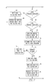
- FIG. 7 is a flowchart illustrating operation of the memory device of FIGS. 3A and 3B according to an exemplary embodiment of the disclosed concept.
- directly coupled means that two elements are directly in contact with each other.
- number shall mean one or an integer greater than one (i.e., a plurality).
- module and “component” are intended to refer to a computer related entity, either hardware (e.g., integrated circuit), a combination of hardware and software (e.g., firmware), software, or software in execution.
- a module or component can be, but is not limited to being, a process running on a processor, a processor itself, an object, an executable, a thread of execution, a program, and/or a computer.
- the disclosed concept provides, in one aspect, an adaptive refreshing scheme which tracks the degradation of memory window over time and refreshes the memory cells of a memory array, such as an FeDRAM array, only when necessary.
- the disclosed scheme reduces the number of refresh operations as well as the incurred energy consumption, and prolongs the lifetime of the memory cells (e.g., FeDRAM cells).
- the read reliability of the memory cells is also improved according to another aspect of the disclosed concept by adaptively adjusting the read voltage to overcome the degradation of the memory window.
- FIGS. 3A and 3B are a schematic diagram of a memory device 20 according to a non-limiting exemplary embodiment of the disclosed concept.
- Exemplary memory device 20 includes a memory array 2 having a plurality of FeFETs 4 arranged in an n row by m column array as described elsewhere herein ( FIG. 1 ). It will be understood, however, that this is meant to be exemplary only and that memory device 20 can also include storage elements or cells arranged in an array that are not FeFET based.
- Memory device 20 further includes control circuitry 22 that is operatively coupled to memory array 2 for controlling the operation thereof as described herein.
- Control circuitry 22 includes a number of modules or components (described in more detail herein) that each perform a different function for controlling operation of memory device 20 .
- the exemplary control circuitry includes a read/write control module 24 , a word line selector and driver module 26 , a bit line selector and driver module 28 , a source line selector and driver module 30 , a refresh control module 32 , a refresh trigger circuit control module 34 , and a trigger check module 36 .
- Read write control module 24 is structured to receive an operation identifier (e.g., a write command identifier or a read command identifier), an address in memory array 2 to which data is to be written or from which data is to be read, and, in the case of a write command, the actual data that is to be written.
- Read/write control module 24 is further structured to control word line selector and driver module 26 , bit line selector and driver module 28 , and source line selector and driver module 30 and apply appropriate bias voltages to selected FeFETs 4 in memory array 2 in order to write data to memory array 2 or read data from a memory array 2 as appropriate.
- memory device 20 further includes a plurality of (i.e., n) refresh trigger circuits 38 , wherein each refresh trigger circuit 38 is associated with a respective one of the n rows of FeFETs 4 in memory array 2 .
- each refresh trigger circuit 38 is structured to produce an output voltage signal that is indicative of an estimate of the degradation of the memory window of one or more of the FeFETs 4 in the associated row.
- Each refresh trigger circuit 38 is operably coupled to refresh trigger circuit control module 34 which is structured to control the biasing of each refresh trigger control circuit 38 as described in detail below.
- each refresh trigger circuit 38 is provided to both tripper check module 36 and an adaptive read voltage generation circuit 40 (the latter is described in greater detail below).
- Trigger check module 36 is coupled to refresh control module 32 and is structured to monitor the output voltages of the refresh trigger circuits 38 .
- refresh control module 32 determines when to initiate the refresh of the FeFETs 4 in a row in memory array 2 by way of read/write control module 24 based upon the output of trigger check module 36 .
- adaptive read voltage generation circuit 36 is structured to generate an adapted/adjusted read voltage for use by read/write control module 24 when reading data from a row of FeFETs 4 in memory array 2 .
- adapted/adjusted read voltage is based upon the outputs of the refresh trigger circuits 38 .
- FIG. 4 is a schematic diagram of refresh trigger circuit 38 according to one particular, non-limiting exemplary embodiment.
- refresh trigger circuit 38 includes a first FeFET 4 a having a first gate 12 a , a first drain 16 a , and a first source 14 a .
- Refresh trigger circuit 38 further includes a second FeFET 4 b having a second gate 12 b , a second drain 16 b , and a second source 14 b .
- First source 14 a is connected to second drain 16 b at a point of interconnection 42 .
- first FeFET 4 a and second FeFET 4 b are connected in series.
- refresh trigger circuit 38 is structured to produce an output voltage that estimates the degradation over time of the memory window of the FeFETs 4 that are in the row of memory array 2 with which refresh trigger circuit 38 is associated.
- this functionality is achieved by first “initializing” refresh trigger circuit 38 by programming first FeFET 4 a to a first state (e.g., logic “1”) and programming second FeFET 4 b to a second state (e.g., logic “1”) different than the first state.
- first predetermined bias when thereafter a first predetermined bias is applied to first drain 16 a , a second predetermined bias is applied to second source 14 b , and a read voltage is applied to first gate 12 a and second gate 12 b , the voltage output produced at point of interconnection 42 will be able to be read. That output voltage will be indicative of the memory window degradation in the row that is associated with refresh trigger circuit 38 . More specifically, after being initialized as described, the polarization level of first FeFET 4 a (F 1 ) and second FeFET 4 b (F 2 ) will start to decay, and the resistances of both first FeFET 4 a and second FeFET 4 b will change accordingly.
- FIG. 5 is a table that illustrates the various bias voltages that must be applied to FeFETs 4 a and 4 b in order to: (i) read the output voltage at point of interconnection 42 (the first row in the table) and, (ii) in two sequential steps (the second and third rows table), program FeFETs 4 a and 4 b to the opposite states just described.
- FIG. 6 is a schematic diagram of adaptive read voltage generation circuit 40 according to an exemplary embodiment of the disclosed concept.
- adaptive read voltage generation circuit 40 is used to adjust the read voltages that are used by control circuitry 22 to perform read operations on memory array 2 .
- adaptive read voltage generation circuit 40 includes a first divider circuit 44 that includes a first divider transistor 46 coupled to a second divider transistor 48 .
- Adaptive read voltage generation circuit 40 further includes a second divider circuit 50 that includes a third divider transistor 52 coupled to a fourth divider transistor 54 .
- second divider circuit 50 is cascaded with first divider circuit 44 .
- the gate voltage of first divider transistor 46 is controlled by the voltage that is output by the refresh trigger circuit 38 that is associated with the row within memory array 2 that is being read. Also, the gate voltage of second divider transistor 48 is controlled by a first bias voltage (V ref1 ), the gate voltage of third divider transistor 52 is controlled by the output of first divider circuit 48 (at the point of interconnection of first divider transistor 46 and second divider transistor 48 ), and the gate voltage of fourth divider transistor 54 is controlled by a second bias voltage (V ref2 ). The output of second divider circuit 50 (at the point of interconnection of third divider transistor 52 and fourth divider transistor 54 ) provides the read voltage that is to be used by read/write control module 24 for reading the identified row in memory array 2 .
- FIG. 7 is a flowchart illustrating operation of memory device 20 according to an exemplary embodiment of the disclosed concept. As described below, during such operation, the degradation of memory window in the rows of memory array 2 is tracked over time and the FeFETs 4 in any row are refreshed only when necessary. As a result, the number of refresh operations and the energy consumption is minimized. In addition, the read voltages employed by memory device 20 are adaptively adjusted to overcome the degradation of the memory window.
- the method begins at step 60 , wherein control circuitry 22 makes a determination as to whether a write operation has been instituted. If the answer at step 60 is yes, then, at step 62 , the data is written to the selected row of memory array 22 by operation of read/write control module 24 and the selector and driver modules 26 , 28 and 30 . Then, at step 64 , the refresh trigger circuit 38 associated with the selected row is “refreshed,” meaning that refresh trigger circuit 38 is initialized as described above such that first FeFET 4 a and second FeFET 4 b thereof are programmed to opposite states (see rows 2 and 3 of the table of FIG. 5 for the bias voltages required to do so in the exemplary embodiment). The method then returns to step 60 .
- step 66 control circuitry 22 makes a determination as to whether a read operation has been instituted. If the answer is no, then the method returns to step 60 . If, however, the answer at step 66 is yes, then the method proceeds to step 68 .
- step 68 the refresh trigger circuit 38 that is associated with the selected row is read (to determine the voltage at point of interconnection 42 ) by applying the biases shown in FIG. 5 .
- step 70 the adjusted read voltage that is to be used for the read operation is determined by adaptive read voltage generation circuit 40 as described herein.
- step 72 a determination is made as to whether a refresh of the row being read is required as determined by the refresh trigger scheme of the disclosed concept.
- the voltage at point of interconnection 42 as determined in step 68 is compared to a predetermined threshold value using, for example, and without limitation, a comparator and an appropriate reference voltage. If the voltage at point of interconnection 42 is greater than or equal to the predetermined threshold value, then a refresh is not required and the method proceeds to step 74 .
- the selected row of memory array 2 is read by operation of read/write control module 24 and the selector and driver modules 26 , 28 and 30 using the read voltage determined in step 70 . Thereafter, the method returns to step 60 .
- step 76 the selected row of memory array 2 is read by operation of read/write control module 24 and the selector and driver modules 26 , 28 and 30 using the read voltage determined in step 70 . Then, at step 78 , the data that has just been read (stored in latches 56 shown in FIG. 3B ) is written back to the selected row by operation of read/write control module 24 and the selector and driver modules 26 , 28 and 30 . The method then proceeds to step 80 . At step 80 , since a write operation has just occurred, the refresh trigger circuit 38 associated with the selected row is “refreshed” as described above. The method then returns to step 60 .
- refresh trigger circuit 38 associated with the row is refreshed.
- the refresh trigger circuit 38 of the selected row is read to determine whether a refresh of the row being read is needed and to determine the read voltage that is to be used.
- a latch 56 is coupled to the source line of each column in memory array 2 .
- Latches 56 are normally transparent. However, if a refresh is triggered, latches 56 become opaque and transmit the last read data, which is the data stored in the row in question. Using the data values from latches 56 as inputs to read/write control module 24 , appropriate logic levels will be rewritten to the cells of memory array 2 as an automated operation.
- each refresh trigger circuit 38 is refreshed each time that associated row is refreshed in order to keep track of memory window for that row.
- any reference signs placed between parentheses shall not be construed as limiting the claim.
- the word “comprising” or “including” does not exclude the presence of elements or steps other than those listed in a claim.
- several of these means may be embodied by one and the same item of hardware.
- the word “a” or “an” preceding an element does not exclude the presence of a plurality of such elements.
- any device claim enumerating several means several of these means may be embodied by one and the same item of hardware.
- the mere fact that certain elements are recited in mutually different dependent claims does not indicate that these elements cannot be used in combination.
Landscapes
- Engineering & Computer Science (AREA)
- Computer Hardware Design (AREA)
- Microelectronics & Electronic Packaging (AREA)
- Databases & Information Systems (AREA)
- Dram (AREA)
Abstract
Description
Claims (20)
Priority Applications (1)
| Application Number | Priority Date | Filing Date | Title |
|---|---|---|---|
| US15/594,807 US10269406B2 (en) | 2016-05-19 | 2017-05-15 | Adaptive refreshing and read voltage control scheme for a memory device such as an FeDRAM |
Applications Claiming Priority (2)
| Application Number | Priority Date | Filing Date | Title |
|---|---|---|---|
| US201662338606P | 2016-05-19 | 2016-05-19 | |
| US15/594,807 US10269406B2 (en) | 2016-05-19 | 2017-05-15 | Adaptive refreshing and read voltage control scheme for a memory device such as an FeDRAM |
Publications (2)
| Publication Number | Publication Date |
|---|---|
| US20170337962A1 US20170337962A1 (en) | 2017-11-23 |
| US10269406B2 true US10269406B2 (en) | 2019-04-23 |
Family
ID=60330988
Family Applications (1)
| Application Number | Title | Priority Date | Filing Date |
|---|---|---|---|
| US15/594,807 Active US10269406B2 (en) | 2016-05-19 | 2017-05-15 | Adaptive refreshing and read voltage control scheme for a memory device such as an FeDRAM |
Country Status (1)
| Country | Link |
|---|---|
| US (1) | US10269406B2 (en) |
Cited By (1)
| Publication number | Priority date | Publication date | Assignee | Title |
|---|---|---|---|---|
| US11790243B1 (en) | 2022-06-30 | 2023-10-17 | International Business Machines Corporation | Ferroelectric field effect transistor for implementation of decision tree |
Families Citing this family (2)
| Publication number | Priority date | Publication date | Assignee | Title |
|---|---|---|---|---|
| US10832765B2 (en) * | 2018-06-29 | 2020-11-10 | Taiwan Semiconductor Manufacturing Co., Ltd. | Variation tolerant read assist circuit for SRAM |
| US11348635B2 (en) | 2020-03-30 | 2022-05-31 | Micron Technology, Inc. | Memory cell biasing techniques during a read operation |
Citations (7)
| Publication number | Priority date | Publication date | Assignee | Title |
|---|---|---|---|---|
| US6067244A (en) * | 1997-10-14 | 2000-05-23 | Yale University | Ferroelectric dynamic random access memory |
| US20040062071A1 (en) * | 2002-09-30 | 2004-04-01 | Rodriguez John Anthony | Ferroelectric memory with wide operating voltage and multi-bit storage per cell |
| US20060221712A1 (en) * | 2005-03-30 | 2006-10-05 | Tyler Lowrey | Using a bit specific reference level to read a memory |
| US20080094914A1 (en) * | 2006-10-20 | 2008-04-24 | Samsung Electronics Co., Ltd. | Methods of restoring data in flash memory devices and related flash memory device memory systems |
| US20130015517A1 (en) * | 2010-02-07 | 2013-01-17 | Yuniarto Widjaja | Semiconductor Memory Device Having Electrically Floating Body Transistor, Semiconductor Memory Device Having Both Volatile and Non-Volatile Functionality and Method of Operating |
| WO2016004388A1 (en) | 2014-07-03 | 2016-01-07 | Yale University | Circuitry for ferroelectric fet-based dynamic random access memory and non-volatile memory |
| US9852785B2 (en) * | 2016-05-27 | 2017-12-26 | Taiwan Semiconductor Manufacturing Company Limited | Memories with metal-ferroelectric-semiconductor (MFS) transistors |
-
2017
- 2017-05-15 US US15/594,807 patent/US10269406B2/en active Active
Patent Citations (8)
| Publication number | Priority date | Publication date | Assignee | Title |
|---|---|---|---|---|
| US6067244A (en) * | 1997-10-14 | 2000-05-23 | Yale University | Ferroelectric dynamic random access memory |
| US20040062071A1 (en) * | 2002-09-30 | 2004-04-01 | Rodriguez John Anthony | Ferroelectric memory with wide operating voltage and multi-bit storage per cell |
| US20060221712A1 (en) * | 2005-03-30 | 2006-10-05 | Tyler Lowrey | Using a bit specific reference level to read a memory |
| US20080094914A1 (en) * | 2006-10-20 | 2008-04-24 | Samsung Electronics Co., Ltd. | Methods of restoring data in flash memory devices and related flash memory device memory systems |
| US20130015517A1 (en) * | 2010-02-07 | 2013-01-17 | Yuniarto Widjaja | Semiconductor Memory Device Having Electrically Floating Body Transistor, Semiconductor Memory Device Having Both Volatile and Non-Volatile Functionality and Method of Operating |
| WO2016004388A1 (en) | 2014-07-03 | 2016-01-07 | Yale University | Circuitry for ferroelectric fet-based dynamic random access memory and non-volatile memory |
| US20170140807A1 (en) * | 2014-07-03 | 2017-05-18 | Yale University | Circuitry for Ferroelectric FET-Based Dynamic Random Access Memory and Non-Violatile Memory |
| US9852785B2 (en) * | 2016-05-27 | 2017-12-26 | Taiwan Semiconductor Manufacturing Company Limited | Memories with metal-ferroelectric-semiconductor (MFS) transistors |
Non-Patent Citations (15)
| Title |
|---|
| Dragan Damjanovic, Hysteresis in Piezoelectric and Ferroelectric Materials, The Science of Hysteresis, vol. 3; I. Mayergoyz and G. Bertotti (Eds.); Elsevier (2005). |
| Ekaterina Yurchuk et al., Impact of Scaling on the Performance of HfO2-Based Ferroelectric Field Effect Transistors; IEEE Transactions on Electron Devices, vol. 61, No. 11, Nov. 2014. |
| Enes Eken et al., A New Field-assisted Access Scheme of STT-RAM with Self-reference Capability, Dept. of Electrical and Computer Engineering, University of Pittsburgh, T.J. Watson Research Center IBM; DAC'14, Jun. 1-5, 2014, San Francisco, CA; licensed to ACM 978-1-4503-2730-May 14, 2006. |
| Enes Eken et al., A New Field-assisted Access Scheme of STT-RAM with Self-reference Capability, Dept. of Electrical and Computer Engineering, University of Pittsburgh, T.J. Watson Research Center IBM; DAC'14, Jun. 1-5, 2014, San Francisco, CA; licensed to ACM 978-1-4503-2730—May 14, 2006. |
| Hang-Tin Lue et al., Device Modeling of Ferroelectric Memory Field-Effect Transistor for the Application of Ferroelectric Random Access Memory; IEEE Transactions on Ultrasonics, Ferroelectrics and Frequency Control, vol. 50, No. 1, Jan. 2003. |
| I. Arias et al., A phenomenological cohesive model of ferroelectric fatigue, Div. of Engineering and Applied Science, California Institute of Technology, Pasadena, CA 91125; Dept. de Matematica Aplicada III, Universitat Politecnica de Catalunya, Barcelona 08034, Spain. |
| IOP Science, Polarization Fatigue Characteristics of Sol-Gel Ferroelectric . . . Film Capacitors; Jpn. J. Appl. Phys. vol. 33 (1994) pp. 3996-4002, Part 1. No. 7A, Jul. 1994. |
| Stefan Mueller et al., From MFM Capacitors Toward Ferroelectric Transistors: Endurance and Disturb Characteristics of HfO2-Based FeFET Devices; IEEE Transactions on Electron Devices, vol. 60, No. 12, Dec. 2013. |
| T.P. Ma, FEDRAM: A Capacitor-less DRAM Based on Ferroelectric-Gated Field-Effect Transistor, Invited Paper, Dept. of Electrical Engineering, Yale University, New Haven, CT; 978-1-4799-3569-Mar. 2014, © 2014 IEEE. |
| T.P. Ma, FEDRAM: A Capacitor-less DRAM Based on Ferroelectric-Gated Field-Effect Transistor, Invited Paper, Dept. of Electrical Engineering, Yale University, New Haven, CT; 978-1-4799-3569—Mar. 2014, © 2014 IEEE. |
| U. Schroeder et al., Non-volatile data storage in HfO2-based ferroelectric FETs; 978-1-4673-2848-Jul. 2012, © 2012 IEEE. |
| U. Schroeder et al., Non-volatile data storage in HfO2-based ferroelectric FETs; 978-1-4673-2848—Jul. 2012, © 2012 IEEE. |
| Xiao Pan et al., Retention mechansim study of the ferroelectric field effect transistor; Appl. Phys., Lett. 99, 013505 (2011); view online: http://dx.doi.org/10.1063/1.3609323. |
| Yixin Luo et al., WARM: Improving NAND Flash Memory Lifetime with Write-hotness Aware Retention Management; 978-1-4673-7619-Aug. 2015, © 2015 IEEE. |
| Yixin Luo et al., WARM: Improving NAND Flash Memory Lifetime with Write-hotness Aware Retention Management; 978-1-4673-7619—Aug. 2015, © 2015 IEEE. |
Cited By (1)
| Publication number | Priority date | Publication date | Assignee | Title |
|---|---|---|---|---|
| US11790243B1 (en) | 2022-06-30 | 2023-10-17 | International Business Machines Corporation | Ferroelectric field effect transistor for implementation of decision tree |
Also Published As
| Publication number | Publication date |
|---|---|
| US20170337962A1 (en) | 2017-11-23 |
Similar Documents
| Publication | Publication Date | Title |
|---|---|---|
| US10014069B2 (en) | Memory device and refresh methods to alleviate the effects of row hammer condition | |
| US9208878B2 (en) | Non-volatile memory based on retention modulation | |
| US7154788B2 (en) | Semiconductor integrated circuit device | |
| US10354716B2 (en) | SRAM based memory structures and methods thereof | |
| JP3913906B2 (en) | Ferroelectric random access memory device | |
| US8164941B2 (en) | Semiconductor memory device with ferroelectric device and refresh method thereof | |
| US7920417B2 (en) | Semiconductor memory device | |
| US11742013B2 (en) | Apparatus and method for controlling erasing data in ferroelectric memory cells | |
| US20140269008A1 (en) | Non-volatile memory using bi-directional resistive elements | |
| US9852785B2 (en) | Memories with metal-ferroelectric-semiconductor (MFS) transistors | |
| US11562782B2 (en) | Fixed voltage sensing in a memory device | |
| JP2012209004A (en) | Semiconductor memory device | |
| US10269406B2 (en) | Adaptive refreshing and read voltage control scheme for a memory device such as an FeDRAM | |
| CN1656565A (en) | Memory array having 2T memory cells | |
| JP2003007051A (en) | Memory and its operating method | |
| US7518917B2 (en) | Nonvolatile memory utilizing MIS memory transistors capable of multiple store operations | |
| US20110305062A1 (en) | Memory cell and memory device using the same | |
| JP2010238361A (en) | Driving circuit for nonvolatile dram, and riving method thereof | |
| JP2008041157A (en) | Memory cell, and nonvolatile storage device | |
| US20230221871A1 (en) | Memory device and operating method thereof | |
| JP2009187658A (en) | Semiconductor integrated circuit device | |
| TW201624485A (en) | Resistance random access memory | |
| KR20220112694A (en) | Dynamic memory with long retention time | |
| WO2024198549A1 (en) | Memory and control method for memory, and storage system and electronic device |
Legal Events
| Date | Code | Title | Description |
|---|---|---|---|
| AS | Assignment |
Owner name: UNIVERSITY OF PITTSBURGH-OF THE COMMONWEALTH SYSTE Free format text: ASSIGNMENT OF ASSIGNORS INTEREST;ASSIGNORS:BAYRAM, ISMAIL;CHEN, YIRAN;SIGNING DATES FROM 20190103 TO 20190115;REEL/FRAME:048198/0558 |
|
| STPP | Information on status: patent application and granting procedure in general |
Free format text: PUBLICATIONS -- ISSUE FEE PAYMENT VERIFIED |
|
| STCF | Information on status: patent grant |
Free format text: PATENTED CASE |
|
| AS | Assignment |
Owner name: JPMORGAN CHASE BANK, N.A., AS ADMINISTRATIVE AGENT, DELAWARE Free format text: SECURITY INTEREST;ASSIGNORS:MICROCHIP TECHNOLOGY INC.;SILICON STORAGE TECHNOLOGY, INC.;ATMEL CORPORATION;AND OTHERS;REEL/FRAME:053311/0305 Effective date: 20200327 |
|
| AS | Assignment |
Owner name: MICROSEMI STORAGE SOLUTIONS, INC., ARIZONA Free format text: RELEASE BY SECURED PARTY;ASSIGNOR:JPMORGAN CHASE BANK, N.A, AS ADMINISTRATIVE AGENT;REEL/FRAME:053466/0011 Effective date: 20200529 Owner name: MICROSEMI CORPORATION, CALIFORNIA Free format text: RELEASE BY SECURED PARTY;ASSIGNOR:JPMORGAN CHASE BANK, N.A, AS ADMINISTRATIVE AGENT;REEL/FRAME:053466/0011 Effective date: 20200529 Owner name: MICROCHIP TECHNOLOGY INC., ARIZONA Free format text: RELEASE BY SECURED PARTY;ASSIGNOR:JPMORGAN CHASE BANK, N.A, AS ADMINISTRATIVE AGENT;REEL/FRAME:053466/0011 Effective date: 20200529 Owner name: SILICON STORAGE TECHNOLOGY, INC., ARIZONA Free format text: RELEASE BY SECURED PARTY;ASSIGNOR:JPMORGAN CHASE BANK, N.A, AS ADMINISTRATIVE AGENT;REEL/FRAME:053466/0011 Effective date: 20200529 Owner name: ATMEL CORPORATION, ARIZONA Free format text: RELEASE BY SECURED PARTY;ASSIGNOR:JPMORGAN CHASE BANK, N.A, AS ADMINISTRATIVE AGENT;REEL/FRAME:053466/0011 Effective date: 20200529 |
|
| AS | Assignment |
Owner name: WELLS FARGO BANK, NATIONAL ASSOCIATION, MINNESOTA Free format text: SECURITY INTEREST;ASSIGNORS:MICROCHIP TECHNOLOGY INC.;SILICON STORAGE TECHNOLOGY, INC.;ATMEL CORPORATION;AND OTHERS;REEL/FRAME:053468/0705 Effective date: 20200529 |
|
| AS | Assignment |
Owner name: WELLS FARGO BANK, NATIONAL ASSOCIATION, AS COLLATERAL AGENT, MINNESOTA Free format text: SECURITY INTEREST;ASSIGNORS:MICROCHIP TECHNOLOGY INCORPORATED;SILICON STORAGE TECHNOLOGY, INC.;ATMEL CORPORATION;AND OTHERS;REEL/FRAME:055671/0612 Effective date: 20201217 |
|
| AS | Assignment |
Owner name: MICROSEMI STORAGE SOLUTIONS, INC., ARIZONA Free format text: RELEASE BY SECURED PARTY;ASSIGNOR:WELLS FARGO BANK, NATIONAL ASSOCIATION, AS NOTES COLLATERAL AGENT;REEL/FRAME:059863/0400 Effective date: 20220228 Owner name: MICROSEMI CORPORATION, ARIZONA Free format text: RELEASE BY SECURED PARTY;ASSIGNOR:WELLS FARGO BANK, NATIONAL ASSOCIATION, AS NOTES COLLATERAL AGENT;REEL/FRAME:059863/0400 Effective date: 20220228 Owner name: ATMEL CORPORATION, ARIZONA Free format text: RELEASE BY SECURED PARTY;ASSIGNOR:WELLS FARGO BANK, NATIONAL ASSOCIATION, AS NOTES COLLATERAL AGENT;REEL/FRAME:059863/0400 Effective date: 20220228 Owner name: SILICON STORAGE TECHNOLOGY, INC., ARIZONA Free format text: RELEASE BY SECURED PARTY;ASSIGNOR:WELLS FARGO BANK, NATIONAL ASSOCIATION, AS NOTES COLLATERAL AGENT;REEL/FRAME:059863/0400 Effective date: 20220228 Owner name: MICROCHIP TECHNOLOGY INCORPORATED, ARIZONA Free format text: RELEASE BY SECURED PARTY;ASSIGNOR:WELLS FARGO BANK, NATIONAL ASSOCIATION, AS NOTES COLLATERAL AGENT;REEL/FRAME:059863/0400 Effective date: 20220228 |
|
| AS | Assignment |
Owner name: MICROSEMI STORAGE SOLUTIONS, INC., ARIZONA Free format text: RELEASE BY SECURED PARTY;ASSIGNOR:WELLS FARGO BANK, NATIONAL ASSOCIATION, AS NOTES COLLATERAL AGENT;REEL/FRAME:060894/0437 Effective date: 20220228 Owner name: MICROSEMI CORPORATION, ARIZONA Free format text: RELEASE BY SECURED PARTY;ASSIGNOR:WELLS FARGO BANK, NATIONAL ASSOCIATION, AS NOTES COLLATERAL AGENT;REEL/FRAME:060894/0437 Effective date: 20220228 Owner name: ATMEL CORPORATION, ARIZONA Free format text: RELEASE BY SECURED PARTY;ASSIGNOR:WELLS FARGO BANK, NATIONAL ASSOCIATION, AS NOTES COLLATERAL AGENT;REEL/FRAME:060894/0437 Effective date: 20220228 Owner name: SILICON STORAGE TECHNOLOGY, INC., ARIZONA Free format text: RELEASE BY SECURED PARTY;ASSIGNOR:WELLS FARGO BANK, NATIONAL ASSOCIATION, AS NOTES COLLATERAL AGENT;REEL/FRAME:060894/0437 Effective date: 20220228 Owner name: MICROCHIP TECHNOLOGY INCORPORATED, ARIZONA Free format text: RELEASE BY SECURED PARTY;ASSIGNOR:WELLS FARGO BANK, NATIONAL ASSOCIATION, AS NOTES COLLATERAL AGENT;REEL/FRAME:060894/0437 Effective date: 20220228 |
|
| MAFP | Maintenance fee payment |
Free format text: PAYMENT OF MAINTENANCE FEE, 4TH YR, SMALL ENTITY (ORIGINAL EVENT CODE: M2551); ENTITY STATUS OF PATENT OWNER: SMALL ENTITY Year of fee payment: 4 |