US10256358B2 - Device for improving the quality of an image covered with a semitransparent photovoltaic film - Google Patents
Device for improving the quality of an image covered with a semitransparent photovoltaic film Download PDFInfo
- Publication number
- US10256358B2 US10256358B2 US14/413,098 US201314413098A US10256358B2 US 10256358 B2 US10256358 B2 US 10256358B2 US 201314413098 A US201314413098 A US 201314413098A US 10256358 B2 US10256358 B2 US 10256358B2
- Authority
- US
- United States
- Prior art keywords
- image
- photovoltaic
- sheet
- luminosity
- light
- Prior art date
- Legal status (The legal status is an assumption and is not a legal conclusion. Google has not performed a legal analysis and makes no representation as to the accuracy of the status listed.)
- Active
Links
- 239000011521 glass Substances 0.000 claims description 11
- 230000015556 catabolic process Effects 0.000 claims description 5
- 238000006731 degradation reaction Methods 0.000 claims description 5
- 229910052710 silicon Inorganic materials 0.000 claims description 3
- 239000010703 silicon Substances 0.000 claims description 3
- 239000011343 solid material Substances 0.000 claims 2
- 230000000007 visual effect Effects 0.000 abstract description 7
- 238000000151 deposition Methods 0.000 abstract 1
- 230000005611 electricity Effects 0.000 description 4
- 230000004438 eyesight Effects 0.000 description 4
- 230000006870 function Effects 0.000 description 4
- 229910052782 aluminium Inorganic materials 0.000 description 3
- XAGFODPZIPBFFR-UHFFFAOYSA-N aluminium Chemical compound [Al] XAGFODPZIPBFFR-UHFFFAOYSA-N 0.000 description 3
- VYZAMTAEIAYCRO-UHFFFAOYSA-N Chromium Chemical compound [Cr] VYZAMTAEIAYCRO-UHFFFAOYSA-N 0.000 description 2
- 230000002745 absorbent Effects 0.000 description 2
- 239000002250 absorbent Substances 0.000 description 2
- 229910021417 amorphous silicon Inorganic materials 0.000 description 2
- 238000010586 diagram Methods 0.000 description 2
- 229910052751 metal Inorganic materials 0.000 description 2
- 239000002184 metal Substances 0.000 description 2
- 239000003973 paint Substances 0.000 description 2
- 230000007704 transition Effects 0.000 description 2
- 239000012780 transparent material Substances 0.000 description 2
- 230000004888 barrier function Effects 0.000 description 1
- 229910021419 crystalline silicon Inorganic materials 0.000 description 1
- 230000000694 effects Effects 0.000 description 1
- 239000000463 material Substances 0.000 description 1
- 238000000034 method Methods 0.000 description 1
- 230000002028 premature Effects 0.000 description 1
- 230000000717 retained effect Effects 0.000 description 1
- 230000016776 visual perception Effects 0.000 description 1
Images

Classifications
-
- H01L31/0468—
-
- H—ELECTRICITY
- H10—SEMICONDUCTOR DEVICES; ELECTRIC SOLID-STATE DEVICES NOT OTHERWISE PROVIDED FOR
- H10F—INORGANIC SEMICONDUCTOR DEVICES SENSITIVE TO INFRARED RADIATION, LIGHT, ELECTROMAGNETIC RADIATION OF SHORTER WAVELENGTH OR CORPUSCULAR RADIATION
- H10F19/00—Integrated devices, or assemblies of multiple devices, comprising at least one photovoltaic cell covered by group H10F10/00, e.g. photovoltaic modules
- H10F19/30—Integrated devices, or assemblies of multiple devices, comprising at least one photovoltaic cell covered by group H10F10/00, e.g. photovoltaic modules comprising thin-film photovoltaic cells
- H10F19/31—Integrated devices, or assemblies of multiple devices, comprising at least one photovoltaic cell covered by group H10F10/00, e.g. photovoltaic modules comprising thin-film photovoltaic cells having multiple laterally adjacent thin-film photovoltaic cells deposited on the same substrate
- H10F19/37—Integrated devices, or assemblies of multiple devices, comprising at least one photovoltaic cell covered by group H10F10/00, e.g. photovoltaic modules comprising thin-film photovoltaic cells having multiple laterally adjacent thin-film photovoltaic cells deposited on the same substrate comprising means for obtaining partial light transmission through the integrated devices, or the assemblies of multiple devices, e.g. partially transparent thin-film photovoltaic modules for windows
-
- G—PHYSICS
- G09—EDUCATION; CRYPTOGRAPHY; DISPLAY; ADVERTISING; SEALS
- G09F—DISPLAYING; ADVERTISING; SIGNS; LABELS OR NAME-PLATES; SEALS
- G09F13/00—Illuminated signs; Luminous advertising
- G09F13/04—Signs, boards or panels, illuminated from behind the insignia
- G09F13/14—Arrangements of reflectors therein
-
- H01L31/048—
-
- H01L31/054—
-
- H01L31/0547—
-
- H—ELECTRICITY
- H02—GENERATION; CONVERSION OR DISTRIBUTION OF ELECTRIC POWER
- H02S—GENERATION OF ELECTRIC POWER BY CONVERSION OF INFRARED RADIATION, VISIBLE LIGHT OR ULTRAVIOLET LIGHT, e.g. USING PHOTOVOLTAIC [PV] MODULES
- H02S40/00—Components or accessories in combination with PV modules, not provided for in groups H02S10/00 - H02S30/00
- H02S40/20—Optical components
- H02S40/22—Light-reflecting or light-concentrating means
-
- H—ELECTRICITY
- H10—SEMICONDUCTOR DEVICES; ELECTRIC SOLID-STATE DEVICES NOT OTHERWISE PROVIDED FOR
- H10F—INORGANIC SEMICONDUCTOR DEVICES SENSITIVE TO INFRARED RADIATION, LIGHT, ELECTROMAGNETIC RADIATION OF SHORTER WAVELENGTH OR CORPUSCULAR RADIATION
- H10F19/00—Integrated devices, or assemblies of multiple devices, comprising at least one photovoltaic cell covered by group H10F10/00, e.g. photovoltaic modules
- H10F19/80—Encapsulations or containers for integrated devices, or assemblies of multiple devices, having photovoltaic cells
-
- H—ELECTRICITY
- H10—SEMICONDUCTOR DEVICES; ELECTRIC SOLID-STATE DEVICES NOT OTHERWISE PROVIDED FOR
- H10F—INORGANIC SEMICONDUCTOR DEVICES SENSITIVE TO INFRARED RADIATION, LIGHT, ELECTROMAGNETIC RADIATION OF SHORTER WAVELENGTH OR CORPUSCULAR RADIATION
- H10F77/00—Constructional details of devices covered by this subclass
- H10F77/40—Optical elements or arrangements
- H10F77/42—Optical elements or arrangements directly associated or integrated with photovoltaic cells, e.g. light-reflecting means or light-concentrating means
- H10F77/488—Reflecting light-concentrating means, e.g. parabolic mirrors or concentrators using total internal reflection
-
- Y—GENERAL TAGGING OF NEW TECHNOLOGICAL DEVELOPMENTS; GENERAL TAGGING OF CROSS-SECTIONAL TECHNOLOGIES SPANNING OVER SEVERAL SECTIONS OF THE IPC; TECHNICAL SUBJECTS COVERED BY FORMER USPC CROSS-REFERENCE ART COLLECTIONS [XRACs] AND DIGESTS
- Y02—TECHNOLOGIES OR APPLICATIONS FOR MITIGATION OR ADAPTATION AGAINST CLIMATE CHANGE
- Y02E—REDUCTION OF GREENHOUSE GAS [GHG] EMISSIONS, RELATED TO ENERGY GENERATION, TRANSMISSION OR DISTRIBUTION
- Y02E10/00—Energy generation through renewable energy sources
- Y02E10/50—Photovoltaic [PV] energy
- Y02E10/52—PV systems with concentrators
Definitions
- the present invention relates to the field of images which are covered with a semitransparent photovoltaic film.
- Devices which produce photovoltaic electricity on the surface of an image generally use a semitransparent photovoltaic sheet laid onto or adhered to the surface of the image.
- This photovoltaic sheet is made up of a transparent sheet on which narrow, parallel photovoltaic strips have been deposited, separated by a distance which is a function of the desired transparency.
- the greater this distance the lower the level of cover of the photovoltaic layer and therefore the greater the transparency.
- the shorter the distance between the photovoltaic strips the greater the level of cover, resulting in a lower transparency. The lower the transparency, the more the image loses in terms of luminosity.
- the photovoltaic layers can also be of any type, made from crystalline or amorphous silicon, or may be made up of multiple photosensitive layers such as CIGS.
- the arrangement of a semitransparent sheet on an image causes a reduction in its luminosity.
- the quantity of light that illuminates the image is reduced by the photovoltaic strips which form an obstacle and which absorb a part of the incident light.
- the image and the photovoltaic sheet are distant from one another, therefore not adhered to one another, a part of the light that is emitted by the image is itself stopped by the photovoltaic cells, which further reduces the apparent luminosity of the image.
- the object of the invention is to reduce the shading effect of photovoltaic cells while retaining the same photovoltaic surface, which will enable the same electrical power to be retained and the luminosity of the image, i.e. its visual quality, to be increased.
- the invention will also make it possible to increase the surface of the photovoltaic cells in a different manner, while retaining the same luminosity, i.e. the visual quality of the image.
- photovoltaic sheet also includes “photovoltaic films” which are thin and flexible photovoltaic sheets.
- image includes all images printed on any medium and electronic images which use ambient light only, and also the surface of any “object”, this surface making up an image which can have any given form.
- the device which forms the subject-matter of the invention is made up of an image on which a semitransparent photovoltaic sheet is positioned.
- the image may be a printed image or an electronic image, for example an LCD image, or an image made up of pixels backlit by mirrors, or the colored surface of any given object, flat or otherwise, such as a wall, tile or table.
- the semitransparent photovoltaic sheet is a transparent sheet, made from rigid or flexible, flat or curved crystalline glass or organic glass, on which crystalline or amorphous photovoltaic cells have been arranged, such as, for example, silicon, or a stacking of thin photosensitive and photovoltaic layers, such as, for example CIGS, or organic cells. These cells may be opaque or semitransparent. They are distributed on the surface of the transparent sheet to form opaque areas separated by transparent areas, or they are distributed in the form of networks of geometric figures such as, for example, rectangular and parallel strips separated by transparent strips.
- These photovoltaic cells have two sides, one of which is turned toward the image or toward the object.
- This side turned toward the image or toward the object is covered with a highly light-reflective layer, such as, for example, an ink or white paint or a mirror-effect aluminum or chrome metal deposit.
- the sides of the photovoltaic cells turned toward the image are suitable for reflecting more than 30% of the light which they receive.
- This reflective side is separated from the image or from the surface of the object by a non-zero distance.
- the space thus created between the reflective side of the photovoltaic cells and the image may comprise air or a transparent material such as crystalline glass or organic glass.
- the image and the sheet which covers it are illuminated by an incident light, one part of which is intercepted by the photovoltaic cells and another part of which crosses the transparent areas and illuminates the image.
- Each pixel of the image then diffuses this light in all directions.
- This light diffused by the image either crosses the transparent areas again as far as the observer, or is reflected by the reflective sides of the photovoltaic cells, or is reflected in the transparent areas when two conditions are satisfied: the refractive index of the space between the cells and the image is greater than air, and the angle of incidence of the light ray is greater than the critical angle of the total reflection in the transition from a high-index diopter to a low-index diopter.
- the device is associated with means for modifying the original image, notably in its brightness, contrast and color saturation characteristics.
- the image receives less light since a part of said light is stopped by the photovoltaic cells. The observer will therefore see an image which is darker, less bright than the original image.
- the original digital image undergoes a computer processing which consists in increasing the luminosity of all or some of its pixels. The percentage of this luminosity increase will be a function of the characteristics of the original image and the percentage of shading of the photovoltaic cells.
- the means for modifying the luminosity of the image are adjusted in order to increase the luminosity of the image by a percentage equal to or greater than the percentage of cover of the photovoltaic cells on the sheet.
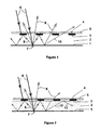
- FIG. 1 is a schematic diagram in cross-section of the device according to the invention.
- FIG. 2 is a schematic diagram in cross-section of a variant of the device with a space with a high refractive index between the cells and the image.
- the device forming the subject-matter of the invention ( FIG. 1 ) is made up of an image ( 7 ) on which a semitransparent photovoltaic sheet is positioned.
- the image ( 7 ) may be a printed image or an electronic image, for example an LCD image, or an image made up of pixels backlit by mirrors, or the colored surface of any given object, flat or otherwise, such as a wall, tile or table.
- the semitransparent photovoltaic sheet is a transparent sheet ( 5 ) made from rigid or flexible, flat or curved crystalline glass or organic glass, on which crystalline or amorphous photovoltaic cells ( 4 ) have been arranged, such as, for example, silicon, or a stacking of thin photosensitive and photovoltaic layers, such as, for example CIGS, or organic cells.
- These cells ( 4 ) may be opaque or semitransparent. They are distributed on the surface of the transparent sheet ( 5 ) to form opaque areas separated by transparent areas, or they are distributed in the form of networks of geometric figures such as, for example, rectangular and parallel strips separated by transparent strips.
- the photovoltaic cells ( 4 ) have two sides, one of which is turned toward the image or toward the object. This side turned toward the image or toward the object is covered with a highly light-reflective layer ( 3 ), such as, for example, an ink or white paint or a mirror-effect aluminum or chrome metal deposit. This reflective side ( 3 ) is separated from the image ( 1 ) or from the surface of the object ( 1 ) by a non-zero distance.
- the space ( 2 ) thus created between the reflective side ( 3 ) of the photovoltaic cells and the image ( 1 ) may comprise air or a transparent material ( FIG. 2 ) such as crystalline glass or organic glass, the refractive index of which is greater than 1.
- the image ( 1 ) and the cells ( 4 ) which cover it are illuminated by an incident light ( 6 ), one part of which is intercepted by the photovoltaic cells ( 4 ) and another part of which crosses the transparent areas and illuminates the image ( 1 ).
- Each pixel ( 7 ) of the image then diffuses this light in all directions ( 8 , 9 , 10 ).
- This light diffused by the image either crosses the transparent areas again as far as the observer ( 9 ), or is reflected by the reflective sides ( 3 ) of the photovoltaic cells ( 4 ), or is reflected ( 10 , 11 ) in the transparent areas ( FIG.
- the refractive index of the space ( 2 ) between the cells ( 4 ) and the image ( 1 ) is greater than air
- the angle of incidence of the light ray ( 10 — FIG. 2 ) is greater than the critical angle of the total reflection in the transition from a high-index diopter to a low-index diopter.
- the original image ( 1 ) is modified notably in its brightness, contrast and color saturation characteristics.
- the image ( 1 ) receives less light since a part of said light is stopped by the photovoltaic cells ( 4 ). The observer will therefore see an image which is darker, less bright than the original image.
- the original digital image undergoes a computer processing which consists in increasing the luminosity of all or some of its pixels.
- the percentage of this increase in luminosity will be a function of the characteristics of the original image and the percentage of shading of the photovoltaic cells. The same will apply to the contrast and color saturation which will be modified so that the vision of the observer most closely approximates the vision of the original image.
- the image ( 1 ) covered with the photovoltaic sheet ( 5 ) will thus produce electricity with a minimum of visual degradation.
- the device according to the invention includes a one-meter-sided, square paper image ( 1 ) and a glass sheet ( 5 ) having the same dimensions and a thickness of 4 mm, on which a network of parallel strips of thin photovoltaic layers ( 4 ) made from amorphous silicon have been deposited, of which the width is 1 mm and the distance separating them is 3 mm.
- the photovoltaic strips ( 4 ) are covered on one of the sides ( 3 ) with a thin-layer, aluminum deposit which has the property of reflecting more than 60% of the light which it receives.
- This side ( 3 ) which is covered with a reflective layer is turned toward the image ( 1 ) and covers it.
- the distance between the photovoltaic sheet and the image is 1 cm.
- This space ( 2 ) contains air only.
- the level of cover of the photovoltaic material on the surface of the sheet is 25%.
- the digital image has been modified before its paper printout ( 1 ) by increasing its luminosity by 30% and reducing its contrast by 5%.
- the photovoltaic sheet ( 5 ) will produce around 15 watts of electrical power in full sunlight while reproducing an image very similar to the original image.
- the invention achieves the defined objects. It is particularly suitable for covering an image or an object with a semitransparent photovoltaic sheet or film while reducing the visual degradation of the image.
Landscapes
- Physics & Mathematics (AREA)
- General Physics & Mathematics (AREA)
- Engineering & Computer Science (AREA)
- Theoretical Computer Science (AREA)
- Photovoltaic Devices (AREA)
- Devices For Indicating Variable Information By Combining Individual Elements (AREA)
- Electroluminescent Light Sources (AREA)
- Mirrors, Picture Frames, Photograph Stands, And Related Fastening Devices (AREA)
- Optical Elements Other Than Lenses (AREA)
Abstract
Description
Claims (8)
Applications Claiming Priority (4)
| Application Number | Priority Date | Filing Date | Title |
|---|---|---|---|
| FR1201927A FR2993087B1 (en) | 2012-07-06 | 2012-07-06 | DEVICE FOR ENHANCING THE QUALITY OF AN IMAGE COVERED WITH A SEMI-TRANSPARENT PHOTOVOLTAIC FILM |
| FR1201927 | 2012-07-06 | ||
| FR12/01927 | 2012-07-06 | ||
| PCT/FR2013/000174 WO2014006282A1 (en) | 2012-07-06 | 2013-07-04 | Device for improving the quality of an image covered with a semitransparent photovoltaic film |
Related Parent Applications (1)
| Application Number | Title | Priority Date | Filing Date |
|---|---|---|---|
| PCT/FR2013/000174 A-371-Of-International WO2014006282A1 (en) | 2012-07-06 | 2013-07-04 | Device for improving the quality of an image covered with a semitransparent photovoltaic film |
Related Child Applications (1)
| Application Number | Title | Priority Date | Filing Date |
|---|---|---|---|
| US16/354,325 Continuation US20190214515A1 (en) | 2012-07-06 | 2019-03-15 | Device for improving the quality of an image covered with a semitransparent photovoltaic film |
Publications (2)
| Publication Number | Publication Date |
|---|---|
| US20150214406A1 US20150214406A1 (en) | 2015-07-30 |
| US10256358B2 true US10256358B2 (en) | 2019-04-09 |
Family
ID=47501296
Family Applications (2)
| Application Number | Title | Priority Date | Filing Date |
|---|---|---|---|
| US14/413,098 Active US10256358B2 (en) | 2012-07-06 | 2013-07-04 | Device for improving the quality of an image covered with a semitransparent photovoltaic film |
| US16/354,325 Abandoned US20190214515A1 (en) | 2012-07-06 | 2019-03-15 | Device for improving the quality of an image covered with a semitransparent photovoltaic film |
Family Applications After (1)
| Application Number | Title | Priority Date | Filing Date |
|---|---|---|---|
| US16/354,325 Abandoned US20190214515A1 (en) | 2012-07-06 | 2019-03-15 | Device for improving the quality of an image covered with a semitransparent photovoltaic film |
Country Status (7)
| Country | Link |
|---|---|
| US (2) | US10256358B2 (en) |
| EP (1) | EP2870638B1 (en) |
| JP (2) | JP2015527605A (en) |
| CN (1) | CN104769728B (en) |
| ES (1) | ES2566372T3 (en) |
| FR (1) | FR2993087B1 (en) |
| WO (1) | WO2014006282A1 (en) |
Cited By (3)
| Publication number | Priority date | Publication date | Assignee | Title |
|---|---|---|---|---|
| CN111725346A (en) * | 2020-06-29 | 2020-09-29 | 杭州福斯特应用材料股份有限公司 | Reflective film and photovoltaic modules |
| US20240178333A1 (en) * | 2019-10-30 | 2024-05-30 | Casio Computer Co., Ltd. | Solar panel, electronic instrument, and electronic timepiece |
| US12512786B2 (en) | 2023-09-29 | 2025-12-30 | Toyota Motor Engineering & Manufacturing North America, Inc. | System to display a vivid image on solar cells |
Families Citing this family (2)
| Publication number | Priority date | Publication date | Assignee | Title |
|---|---|---|---|---|
| EP3092674A4 (en) * | 2014-01-10 | 2017-08-16 | Nokia Technologies OY | Method and apparatus for modifying image to increase solar energy collection efficiency |
| KR102168720B1 (en) * | 2018-07-24 | 2020-10-22 | 엘지디스플레이 주식회사 | display device having a mirror function |
Citations (10)
| Publication number | Priority date | Publication date | Assignee | Title |
|---|---|---|---|---|
| US3990100A (en) * | 1974-10-09 | 1976-11-02 | Sony Corporation | Semiconductor device having an antireflective coating |
| US5101260A (en) * | 1989-05-01 | 1992-03-31 | Energy Conversion Devices, Inc. | Multilayer light scattering photovoltaic back reflector and method of making same |
| JPH11296636A (en) | 1998-04-15 | 1999-10-29 | Toppan Printing Co Ltd | IC card with reflective display with solar cells |
| US6133521A (en) * | 1997-03-13 | 2000-10-17 | Sanyo Electric Co., Ltd. | Solar battery output section and its method of manufacture |
| US20030227435A1 (en) * | 2002-06-06 | 2003-12-11 | Chang-Fa Hsieh | Method for adjusting and detecting brightness of liquid crystal displays |
| US6791905B1 (en) * | 1998-11-26 | 2004-09-14 | Citizen Watch Co., Ltd. | Timepiece |
| WO2005071760A1 (en) | 2004-01-23 | 2005-08-04 | Origin Energy Solar Pty Ltd | Solar panel |
| US20050172997A1 (en) * | 2004-02-06 | 2005-08-11 | Johannes Meier | Back contact and back reflector for thin film silicon solar cells |
| FR2896596A1 (en) | 2006-01-26 | 2007-07-27 | Joel Gilbert | OPTICAL SYSTEM FOR VISUALIZING AN IMAGE ON THE SURFACE OF A SOLAR PANEL |
| JP2008072004A (en) | 2006-09-15 | 2008-03-27 | Msk Corp | Transmission-type solar light generating apparatus |
Family Cites Families (13)
| Publication number | Priority date | Publication date | Assignee | Title |
|---|---|---|---|---|
| US4342044A (en) * | 1978-03-08 | 1982-07-27 | Energy Conversion Devices, Inc. | Method for optimizing photoresponsive amorphous alloys and devices |
| US4379943A (en) * | 1981-12-14 | 1983-04-12 | Energy Conversion Devices, Inc. | Current enhanced photovoltaic device |
| US4816324A (en) * | 1986-05-14 | 1989-03-28 | Atlantic Richfield Company | Flexible photovoltaic device |
| JPS63138593U (en) * | 1987-03-03 | 1988-09-12 | ||
| JP3983911B2 (en) * | 1998-12-22 | 2007-09-26 | シチズンホールディングス株式会社 | Liquid crystal display |
| AU2000226369B2 (en) * | 2000-02-02 | 2006-01-19 | Brilliant Film, Llc | Multiflecting light directing film |
| JP2002333618A (en) * | 2001-05-07 | 2002-11-22 | Nitto Denko Corp | Reflective liquid crystal display |
| US7417782B2 (en) * | 2005-02-23 | 2008-08-26 | Pixtronix, Incorporated | Methods and apparatus for spatial light modulation |
| KR101112548B1 (en) * | 2004-12-10 | 2012-02-15 | 삼성전자주식회사 | Microlens substrate for three-dimensional display device, three-dimensional display device and manufacturing method thereof |
| KR20100038684A (en) * | 2008-10-06 | 2010-04-15 | 삼성전자주식회사 | Back light unit and image display device using thereof |
| US20110048493A1 (en) * | 2009-09-02 | 2011-03-03 | Electronics And Telecommunications Research Institute | Solar cell |
| EP2577742A2 (en) * | 2010-06-07 | 2013-04-10 | Semprius, Inc. | Photovoltaic devices with off-axis image display |
| JP2012064550A (en) * | 2010-09-17 | 2012-03-29 | Fujikura Ltd | Dye-sensitized solar cell and display with dye-sensitized solar cell |
-
2012
- 2012-07-06 FR FR1201927A patent/FR2993087B1/en active Active
-
2013
- 2013-07-04 JP JP2015519276A patent/JP2015527605A/en active Pending
- 2013-07-04 EP EP13756534.7A patent/EP2870638B1/en active Active
- 2013-07-04 US US14/413,098 patent/US10256358B2/en active Active
- 2013-07-04 ES ES13756534.7T patent/ES2566372T3/en active Active
- 2013-07-04 CN CN201380046612.8A patent/CN104769728B/en active Active
- 2013-07-04 WO PCT/FR2013/000174 patent/WO2014006282A1/en not_active Ceased
-
2018
- 2018-06-18 JP JP2018115457A patent/JP6684311B2/en active Active
-
2019
- 2019-03-15 US US16/354,325 patent/US20190214515A1/en not_active Abandoned
Patent Citations (12)
| Publication number | Priority date | Publication date | Assignee | Title |
|---|---|---|---|---|
| US3990100A (en) * | 1974-10-09 | 1976-11-02 | Sony Corporation | Semiconductor device having an antireflective coating |
| US5101260A (en) * | 1989-05-01 | 1992-03-31 | Energy Conversion Devices, Inc. | Multilayer light scattering photovoltaic back reflector and method of making same |
| US6133521A (en) * | 1997-03-13 | 2000-10-17 | Sanyo Electric Co., Ltd. | Solar battery output section and its method of manufacture |
| JPH11296636A (en) | 1998-04-15 | 1999-10-29 | Toppan Printing Co Ltd | IC card with reflective display with solar cells |
| US6791905B1 (en) * | 1998-11-26 | 2004-09-14 | Citizen Watch Co., Ltd. | Timepiece |
| US20030227435A1 (en) * | 2002-06-06 | 2003-12-11 | Chang-Fa Hsieh | Method for adjusting and detecting brightness of liquid crystal displays |
| WO2005071760A1 (en) | 2004-01-23 | 2005-08-04 | Origin Energy Solar Pty Ltd | Solar panel |
| US20070277810A1 (en) | 2004-01-23 | 2007-12-06 | Origin Energy Solar Pty Ltd | Solar Panel |
| US20050172997A1 (en) * | 2004-02-06 | 2005-08-11 | Johannes Meier | Back contact and back reflector for thin film silicon solar cells |
| FR2896596A1 (en) | 2006-01-26 | 2007-07-27 | Joel Gilbert | OPTICAL SYSTEM FOR VISUALIZING AN IMAGE ON THE SURFACE OF A SOLAR PANEL |
| US20110063729A1 (en) | 2006-01-26 | 2011-03-17 | Joel Gilbert | Optical system for displaying an image on the surface of a solar panel |
| JP2008072004A (en) | 2006-09-15 | 2008-03-27 | Msk Corp | Transmission-type solar light generating apparatus |
Non-Patent Citations (1)
| Title |
|---|
| International Search Report (PCT/ISA/210) dated Oct. 7, 2013, by the European Patent Office as the International Searching Authority for International Application No. PCT/FR2013/000174. |
Cited By (5)
| Publication number | Priority date | Publication date | Assignee | Title |
|---|---|---|---|---|
| US20240178333A1 (en) * | 2019-10-30 | 2024-05-30 | Casio Computer Co., Ltd. | Solar panel, electronic instrument, and electronic timepiece |
| US12349471B2 (en) * | 2019-10-30 | 2025-07-01 | Casio Computer Co., Ltd. | Solar panel, electronic instrument, and electronic timepiece |
| CN111725346A (en) * | 2020-06-29 | 2020-09-29 | 杭州福斯特应用材料股份有限公司 | Reflective film and photovoltaic modules |
| US12512786B2 (en) | 2023-09-29 | 2025-12-30 | Toyota Motor Engineering & Manufacturing North America, Inc. | System to display a vivid image on solar cells |
| US12549127B2 (en) | 2023-09-29 | 2026-02-10 | Toyota Motor Engineering & Manufacturing North America, Inc. | System to display a vivid image on solar cells having flexible properties |
Also Published As
| Publication number | Publication date |
|---|---|
| JP2015527605A (en) | 2015-09-17 |
| WO2014006282A1 (en) | 2014-01-09 |
| EP2870638B1 (en) | 2016-01-13 |
| FR2993087A1 (en) | 2014-01-10 |
| US20190214515A1 (en) | 2019-07-11 |
| CN104769728B (en) | 2016-11-02 |
| JP2018173651A (en) | 2018-11-08 |
| ES2566372T3 (en) | 2016-04-12 |
| US20150214406A1 (en) | 2015-07-30 |
| FR2993087B1 (en) | 2014-06-27 |
| CN104769728A (en) | 2015-07-08 |
| JP6684311B2 (en) | 2020-04-22 |
| EP2870638A1 (en) | 2015-05-13 |
Similar Documents
| Publication | Publication Date | Title |
|---|---|---|
| US20190214515A1 (en) | Device for improving the quality of an image covered with a semitransparent photovoltaic film | |
| US20040263969A1 (en) | Lenticular antireflection display | |
| JP2020166290A (en) | Video display transparent member, video display system and video display method | |
| CN103943033B (en) | Transparent display device | |
| US10127890B2 (en) | Display device with better contrast | |
| US20140300710A1 (en) | Display unit and electronic apparatus | |
| US20220404530A1 (en) | Display device | |
| WO2022004581A1 (en) | Display apparatus, and optical device | |
| US20230411572A1 (en) | Led array between flexible and rigid substrates | |
| US20210356642A1 (en) | Reflective display device and front light source module thereof | |
| CN103542276B (en) | Reflective display panel realizes the method for radiant evenly | |
| US9904141B2 (en) | Reflective display device | |
| CN206147215U (en) | Anti -dazzle structure, various membrane base plate and display device for display device | |
| US20250060705A1 (en) | Holographic decorated glass for screen color matching | |
| CN215182974U (en) | Device for realizing frameless imaging | |
| US20230395015A1 (en) | Systems With External Displays | |
| KR100996685B1 (en) | Advertising lighting panel, pattern paper sheet for this, and method of manufacturing the pattern paper sheet | |
| CN217879700U (en) | Anti-light screen based on Fresnel lens | |
| CN215182972U (en) | Model imaging device based on medium-free aerial imaging | |
| WO2023240007A1 (en) | Systems with external displays | |
| CN207867206U (en) | Projection film and vehicle-mounted projection device | |
| CN109545096A (en) | Outdoor advertisement machine | |
| CN101103298A (en) | Components for displaying 3D images | |
| WO2008108274A1 (en) | Image display device | |
| JP2015515014A (en) | A method for improving the visual quality of images covered by translucent functional surfaces |
Legal Events
| Date | Code | Title | Description |
|---|---|---|---|
| AS | Assignment |
Owner name: SUNPARTNER TECHNOLOGIES, FRANCE Free format text: ASSIGNMENT OF ASSIGNORS INTEREST;ASSIGNOR:GILBERT, JOEL;REEL/FRAME:035583/0475 Effective date: 20141220 |
|
| STCF | Information on status: patent grant |
Free format text: PATENTED CASE |
|
| AS | Assignment |
Owner name: GARMIN SWITZERLAND GMBH, SWITZERLAND Free format text: ASSIGNMENT OF ASSIGNORS INTEREST;ASSIGNOR:SUNPARTNER TECHNOLOGIES;REEL/FRAME:048912/0375 Effective date: 20190401 |
|
| FEPP | Fee payment procedure |
Free format text: ENTITY STATUS SET TO UNDISCOUNTED (ORIGINAL EVENT CODE: BIG.); ENTITY STATUS OF PATENT OWNER: LARGE ENTITY |
|
| MAFP | Maintenance fee payment |
Free format text: PAYMENT OF MAINTENANCE FEE, 4TH YEAR, LARGE ENTITY (ORIGINAL EVENT CODE: M1551); ENTITY STATUS OF PATENT OWNER: LARGE ENTITY Year of fee payment: 4 |