US10256092B2 - Fabrication of semiconductor structures - Google Patents
Fabrication of semiconductor structures Download PDFInfo
- Publication number
- US10256092B2 US10256092B2 US15/627,965 US201715627965A US10256092B2 US 10256092 B2 US10256092 B2 US 10256092B2 US 201715627965 A US201715627965 A US 201715627965A US 10256092 B2 US10256092 B2 US 10256092B2
- Authority
- US
- United States
- Prior art keywords
- semiconductor
- layer
- spacer
- substrate
- insulating layer
- Prior art date
- Legal status (The legal status is an assumption and is not a legal conclusion. Google has not performed a legal analysis and makes no representation as to the accuracy of the status listed.)
- Active, expires
Links
Images


Classifications
-
- H—ELECTRICITY
- H01—ELECTRIC ELEMENTS
- H01L—SEMICONDUCTOR DEVICES NOT COVERED BY CLASS H10
- H01L21/00—Processes or apparatus adapted for the manufacture or treatment of semiconductor or solid state devices or of parts thereof
- H01L21/02—Manufacture or treatment of semiconductor devices or of parts thereof
- H01L21/02104—Forming layers
- H01L21/02365—Forming inorganic semiconducting materials on a substrate
- H01L21/02612—Formation types
- H01L21/02617—Deposition types
- H01L21/02636—Selective deposition, e.g. simultaneous growth of mono- and non-monocrystalline semiconductor materials
- H01L21/02639—Preparation of substrate for selective deposition
-
- H10P14/271—
-
- H—ELECTRICITY
- H01—ELECTRIC ELEMENTS
- H01L—SEMICONDUCTOR DEVICES NOT COVERED BY CLASS H10
- H01L21/00—Processes or apparatus adapted for the manufacture or treatment of semiconductor or solid state devices or of parts thereof
- H01L21/02—Manufacture or treatment of semiconductor devices or of parts thereof
- H01L21/02104—Forming layers
- H01L21/02365—Forming inorganic semiconducting materials on a substrate
- H01L21/02367—Substrates
- H01L21/0237—Materials
- H01L21/02373—Group 14 semiconducting materials
- H01L21/02381—Silicon, silicon germanium, germanium
-
- H—ELECTRICITY
- H01—ELECTRIC ELEMENTS
- H01L—SEMICONDUCTOR DEVICES NOT COVERED BY CLASS H10
- H01L21/00—Processes or apparatus adapted for the manufacture or treatment of semiconductor or solid state devices or of parts thereof
- H01L21/02—Manufacture or treatment of semiconductor devices or of parts thereof
- H01L21/02104—Forming layers
- H01L21/02365—Forming inorganic semiconducting materials on a substrate
- H01L21/02436—Intermediate layers between substrates and deposited layers
- H01L21/02439—Materials
- H01L21/02488—Insulating materials
-
- H—ELECTRICITY
- H01—ELECTRIC ELEMENTS
- H01L—SEMICONDUCTOR DEVICES NOT COVERED BY CLASS H10
- H01L21/00—Processes or apparatus adapted for the manufacture or treatment of semiconductor or solid state devices or of parts thereof
- H01L21/02—Manufacture or treatment of semiconductor devices or of parts thereof
- H01L21/02104—Forming layers
- H01L21/02365—Forming inorganic semiconducting materials on a substrate
- H01L21/02518—Deposited layers
- H01L21/02521—Materials
- H01L21/02538—Group 13/15 materials
-
- H—ELECTRICITY
- H01—ELECTRIC ELEMENTS
- H01L—SEMICONDUCTOR DEVICES NOT COVERED BY CLASS H10
- H01L21/00—Processes or apparatus adapted for the manufacture or treatment of semiconductor or solid state devices or of parts thereof
- H01L21/02—Manufacture or treatment of semiconductor devices or of parts thereof
- H01L21/04—Manufacture or treatment of semiconductor devices or of parts thereof the devices having potential barriers, e.g. a PN junction, depletion layer or carrier concentration layer
- H01L21/18—Manufacture or treatment of semiconductor devices or of parts thereof the devices having potential barriers, e.g. a PN junction, depletion layer or carrier concentration layer the devices having semiconductor bodies comprising elements of Group IV of the Periodic Table or AIIIBV compounds with or without impurities, e.g. doping materials
- H01L21/30—Treatment of semiconductor bodies using processes or apparatus not provided for in groups H01L21/20 - H01L21/26
- H01L21/302—Treatment of semiconductor bodies using processes or apparatus not provided for in groups H01L21/20 - H01L21/26 to change their surface-physical characteristics or shape, e.g. etching, polishing, cutting
- H01L21/306—Chemical or electrical treatment, e.g. electrolytic etching
- H01L21/3065—Plasma etching; Reactive-ion etching
-
- H—ELECTRICITY
- H01—ELECTRIC ELEMENTS
- H01L—SEMICONDUCTOR DEVICES NOT COVERED BY CLASS H10
- H01L21/00—Processes or apparatus adapted for the manufacture or treatment of semiconductor or solid state devices or of parts thereof
- H01L21/02—Manufacture or treatment of semiconductor devices or of parts thereof
- H01L21/04—Manufacture or treatment of semiconductor devices or of parts thereof the devices having potential barriers, e.g. a PN junction, depletion layer or carrier concentration layer
- H01L21/18—Manufacture or treatment of semiconductor devices or of parts thereof the devices having potential barriers, e.g. a PN junction, depletion layer or carrier concentration layer the devices having semiconductor bodies comprising elements of Group IV of the Periodic Table or AIIIBV compounds with or without impurities, e.g. doping materials
- H01L21/30—Treatment of semiconductor bodies using processes or apparatus not provided for in groups H01L21/20 - H01L21/26
- H01L21/31—Treatment of semiconductor bodies using processes or apparatus not provided for in groups H01L21/20 - H01L21/26 to form insulating layers thereon, e.g. for masking or by using photolithographic techniques; After treatment of these layers; Selection of materials for these layers
- H01L21/3105—After-treatment
- H01L21/311—Etching the insulating layers by chemical or physical means
- H01L21/31105—Etching inorganic layers
- H01L21/31111—Etching inorganic layers by chemical means
- H01L21/31116—Etching inorganic layers by chemical means by dry-etching
-
- H01L21/823807—
-
- H01L21/8258—
-
- H01L21/84—
-
- H01L27/092—
-
- H01L27/1203—
-
- H01L27/1207—
-
- H01L29/0673—
-
- H01L29/66742—
-
- H01L29/78681—
-
- H01L29/78684—
-
- H01L29/78696—
-
- H—ELECTRICITY
- H10—SEMICONDUCTOR DEVICES; ELECTRIC SOLID-STATE DEVICES NOT OTHERWISE PROVIDED FOR
- H10D—INORGANIC ELECTRIC SEMICONDUCTOR DEVICES
- H10D30/00—Field-effect transistors [FET]
- H10D30/01—Manufacture or treatment
- H10D30/021—Manufacture or treatment of FETs having insulated gates [IGFET]
- H10D30/031—Manufacture or treatment of FETs having insulated gates [IGFET] of thin-film transistors [TFT]
-
- H—ELECTRICITY
- H10—SEMICONDUCTOR DEVICES; ELECTRIC SOLID-STATE DEVICES NOT OTHERWISE PROVIDED FOR
- H10D—INORGANIC ELECTRIC SEMICONDUCTOR DEVICES
- H10D30/00—Field-effect transistors [FET]
- H10D30/60—Insulated-gate field-effect transistors [IGFET]
- H10D30/67—Thin-film transistors [TFT]
- H10D30/674—Thin-film transistors [TFT] characterised by the active materials
- H10D30/6741—Group IV materials, e.g. germanium or silicon carbide
-
- H—ELECTRICITY
- H10—SEMICONDUCTOR DEVICES; ELECTRIC SOLID-STATE DEVICES NOT OTHERWISE PROVIDED FOR
- H10D—INORGANIC ELECTRIC SEMICONDUCTOR DEVICES
- H10D30/00—Field-effect transistors [FET]
- H10D30/60—Insulated-gate field-effect transistors [IGFET]
- H10D30/67—Thin-film transistors [TFT]
- H10D30/674—Thin-film transistors [TFT] characterised by the active materials
- H10D30/675—Group III-V materials, Group II-VI materials, Group IV-VI materials, selenium or tellurium
-
- H—ELECTRICITY
- H10—SEMICONDUCTOR DEVICES; ELECTRIC SOLID-STATE DEVICES NOT OTHERWISE PROVIDED FOR
- H10D—INORGANIC ELECTRIC SEMICONDUCTOR DEVICES
- H10D30/00—Field-effect transistors [FET]
- H10D30/60—Insulated-gate field-effect transistors [IGFET]
- H10D30/67—Thin-film transistors [TFT]
- H10D30/6757—Thin-film transistors [TFT] characterised by the structure of the channel, e.g. transverse or longitudinal shape or doping profile
-
- H—ELECTRICITY
- H10—SEMICONDUCTOR DEVICES; ELECTRIC SOLID-STATE DEVICES NOT OTHERWISE PROVIDED FOR
- H10D—INORGANIC ELECTRIC SEMICONDUCTOR DEVICES
- H10D62/00—Semiconductor bodies, or regions thereof, of devices having potential barriers
- H10D62/10—Shapes, relative sizes or dispositions of the regions of the semiconductor bodies; Shapes of the semiconductor bodies
- H10D62/117—Shapes of semiconductor bodies
- H10D62/118—Nanostructure semiconductor bodies
- H10D62/119—Nanowire, nanosheet or nanotube semiconductor bodies
- H10D62/121—Nanowire, nanosheet or nanotube semiconductor bodies oriented parallel to substrates
-
- H—ELECTRICITY
- H10—SEMICONDUCTOR DEVICES; ELECTRIC SOLID-STATE DEVICES NOT OTHERWISE PROVIDED FOR
- H10D—INORGANIC ELECTRIC SEMICONDUCTOR DEVICES
- H10D84/00—Integrated devices formed in or on semiconductor substrates that comprise only semiconducting layers, e.g. on Si wafers or on GaAs-on-Si wafers
- H10D84/01—Manufacture or treatment
- H10D84/0123—Integrating together multiple components covered by H10D12/00 or H10D30/00, e.g. integrating multiple IGBTs
- H10D84/0126—Integrating together multiple components covered by H10D12/00 or H10D30/00, e.g. integrating multiple IGBTs the components including insulated gates, e.g. IGFETs
- H10D84/0165—Integrating together multiple components covered by H10D12/00 or H10D30/00, e.g. integrating multiple IGBTs the components including insulated gates, e.g. IGFETs the components including complementary IGFETs, e.g. CMOS devices
- H10D84/0167—Manufacturing their channels
-
- H—ELECTRICITY
- H10—SEMICONDUCTOR DEVICES; ELECTRIC SOLID-STATE DEVICES NOT OTHERWISE PROVIDED FOR
- H10D—INORGANIC ELECTRIC SEMICONDUCTOR DEVICES
- H10D84/00—Integrated devices formed in or on semiconductor substrates that comprise only semiconducting layers, e.g. on Si wafers or on GaAs-on-Si wafers
- H10D84/01—Manufacture or treatment
- H10D84/02—Manufacture or treatment characterised by using material-based technologies
- H10D84/03—Manufacture or treatment characterised by using material-based technologies using Group IV technology, e.g. silicon technology or silicon-carbide [SiC] technology
- H10D84/038—Manufacture or treatment characterised by using material-based technologies using Group IV technology, e.g. silicon technology or silicon-carbide [SiC] technology using silicon technology, e.g. SiGe
-
- H—ELECTRICITY
- H10—SEMICONDUCTOR DEVICES; ELECTRIC SOLID-STATE DEVICES NOT OTHERWISE PROVIDED FOR
- H10D—INORGANIC ELECTRIC SEMICONDUCTOR DEVICES
- H10D84/00—Integrated devices formed in or on semiconductor substrates that comprise only semiconducting layers, e.g. on Si wafers or on GaAs-on-Si wafers
- H10D84/01—Manufacture or treatment
- H10D84/02—Manufacture or treatment characterised by using material-based technologies
- H10D84/08—Manufacture or treatment characterised by using material-based technologies using combinations of technologies, e.g. using both Si and SiC technologies or using both Si and Group III-V technologies
-
- H—ELECTRICITY
- H10—SEMICONDUCTOR DEVICES; ELECTRIC SOLID-STATE DEVICES NOT OTHERWISE PROVIDED FOR
- H10D—INORGANIC ELECTRIC SEMICONDUCTOR DEVICES
- H10D84/00—Integrated devices formed in or on semiconductor substrates that comprise only semiconducting layers, e.g. on Si wafers or on GaAs-on-Si wafers
- H10D84/80—Integrated devices formed in or on semiconductor substrates that comprise only semiconducting layers, e.g. on Si wafers or on GaAs-on-Si wafers characterised by the integration of at least one component covered by groups H10D12/00 or H10D30/00, e.g. integration of IGFETs
- H10D84/82—Integrated devices formed in or on semiconductor substrates that comprise only semiconducting layers, e.g. on Si wafers or on GaAs-on-Si wafers characterised by the integration of at least one component covered by groups H10D12/00 or H10D30/00, e.g. integration of IGFETs of only field-effect components
- H10D84/83—Integrated devices formed in or on semiconductor substrates that comprise only semiconducting layers, e.g. on Si wafers or on GaAs-on-Si wafers characterised by the integration of at least one component covered by groups H10D12/00 or H10D30/00, e.g. integration of IGFETs of only field-effect components of only insulated-gate FETs [IGFET]
- H10D84/85—Complementary IGFETs, e.g. CMOS
-
- H—ELECTRICITY
- H10—SEMICONDUCTOR DEVICES; ELECTRIC SOLID-STATE DEVICES NOT OTHERWISE PROVIDED FOR
- H10D—INORGANIC ELECTRIC SEMICONDUCTOR DEVICES
- H10D86/00—Integrated devices formed in or on insulating or conducting substrates, e.g. formed in silicon-on-insulator [SOI] substrates or on stainless steel or glass substrates
- H10D86/01—Manufacture or treatment
-
- H—ELECTRICITY
- H10—SEMICONDUCTOR DEVICES; ELECTRIC SOLID-STATE DEVICES NOT OTHERWISE PROVIDED FOR
- H10D—INORGANIC ELECTRIC SEMICONDUCTOR DEVICES
- H10D86/00—Integrated devices formed in or on insulating or conducting substrates, e.g. formed in silicon-on-insulator [SOI] substrates or on stainless steel or glass substrates
- H10D86/201—Integrated devices formed in or on insulating or conducting substrates, e.g. formed in silicon-on-insulator [SOI] substrates or on stainless steel or glass substrates the substrates comprising an insulating layer on a semiconductor body, e.g. SOI
-
- H—ELECTRICITY
- H10—SEMICONDUCTOR DEVICES; ELECTRIC SOLID-STATE DEVICES NOT OTHERWISE PROVIDED FOR
- H10D—INORGANIC ELECTRIC SEMICONDUCTOR DEVICES
- H10D87/00—Integrated devices comprising both bulk components and either SOI or SOS components on the same substrate
-
- H10P14/2902—
-
- H10P14/2905—
-
- H10P14/3238—
-
- H10P14/3402—
-
- H10P14/3414—
-
- H10P50/242—
-
- H10P50/283—
Definitions
- Further steps comprise selectively removing the sacrificial material, thereby forming a first cavity; selectively removing the spacer, thereby forming a second cavity connecting the first cavity to a seed surface of the substrate and growing from the seed surface via the second cavity a replacement structure comprising a semiconductor material in the first cavity. Thereby the sacrificial material is replaced with the semiconductor material.
- the step of forming the spacer comprises patterning the insulating layer in vertical alignment to an outer edge of the sacrificial structure, thereby exposing the seed surface of the substrate; forming the spacer layer by conformal deposition of the spacer material on the exposed seed surface of the substrate and on exposed surfaces of the sacrificial layer and the insulating layer.
- Such an active layer may also be denoted as functional layer as it is involved in the functional behavior of the semiconductor device.
- an active layer is opposed to passive components/layers of the semiconductor device such as a substrate, substrate layer or bulk substrate which provide only mechanical/fabrication support, but are not actively involved in the function of the semiconductor device.
- a first semiconductor device on the first semiconductor structure forming a cavity layer on the first semiconductor device, the first and the second spacer and the sacrificial structure; forming an opening in the cavity layer of the sacrificial structure, thereby exposing a surface of the sacrificial structure; selectively removing the first semiconductor material of the sacrificial structure, thereby forming the first cavity; selectively removing the second spacer, thereby forming the second cavity connecting the first cavity to the seed surface of the substrate; growing from the seed surface via the second cavity a second semiconductor structure as replacement structure comprising a second semiconductor material different from the first semiconductor material in the first cavity structure, thereby replacing the first semiconductor material with the second semiconductor material and forming a second semiconductor device on the second semiconductor structure.
- the invention is embodied as a semiconductor circuit obtainable by methods according to embodiments of the first aspect.
- FIG. 12 shows a top view of the structure of FIG. 11 ;
- FIG. 3 shows a cross-sectional view of a structure 300 after the insulating layer 111 has been patterned in vertical alignment to an outer edge 310 of the sacrificial structure 120 . More particularly, the insulating layer 111 has been patterned and etched down to the substrate 110 at at least one edge of (or through a part of) the sacrificial structure 120 but preferably only one location (edge or part) for single crystalline material formation. This has formed a sidewall 312 in the protection layer 121 , the sacrificial structure 120 and the insulating layer 111 . This can be done by suitable lithography and subsequent etching steps. As a result, a seed surface 311 , adjacent to the sidewall 312 , has been formed in order to act as a seed surface for growing a semiconductor structure.
- FIG. 5 shows a cross-sectional view of a structure 500 after a spacer 510 has been formed at the sidewall 312 of the insulating layer 111 and the sacrificial structure 120 by selectively etching the spacer layer 410 .
- the spacer 510 may be formed e.g. by dry etching the spacer layer 410 by Inductively Coupled Plasma (ICP) etching, Reactive Ion Etching (RIE), Electron Cyclotron Resonance (ECR) etching, or Helicon etching. These techniques allow a precise control of the etching process and hence a precise control of the formation of the spacer 510 .
- ICP Inductively Coupled Plasma
- RIE Reactive Ion Etching
- ECR Electron Cyclotron Resonance
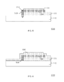
- FIG. 16 shows a cross-sectional view of a structure 1600 after forming a first semiconductor device 1620 on the first semiconductor structure 1310 .
- the first semiconductor device 1620 is a field effect transistor (FET) 1620 and the first semiconductor structure 1310 comprises a channel structure 1312 of the FET 1620 .
- the channel structure 1312 may have a thickness of, for example, about 5 nm that corresponds to a desired channel thickness of the FET 1620 .
- the FET 1620 may be in particular a pFET.
- the gate stack 1630 may comprises a gate dielectric layer, a gate metal layer and a gate cap layer.
- the raised source layer 1625 and the raised drain layer 1626 may be formed by selective epitaxy.
- the ratio x of Si in the SiGe alloy of the raised source layer 1625 and the raised drain layer 1626 may be different from the ratio x of Si in the SiGe alloy of the channel structure 1312 . Such a different ratio may induce strain in the channel structure 1312 which results in a compressed channel structure 1312 and an improved device performance.
- the raised source layer 1625 and the raised drain layer 1626 may be doped with a p-type dopant, e.g. with boron (B). The doping can be preferably performed by in-situ doping during the selective epitaxy step.
- the gate dielectric layer, the gate metal layer and the gate cap layer may comprise materials as described with reference to FIG. 16 .
- insulating spacers 2135 have been formed that insulate the gate stack 2130 from a raised source layer 2125 and a raised drain layer 2126 .
- the raised source layer 2125 and the raised drain layer 2126 may be formed by selective epitaxy.
- the raised source layer 2125 and the raised drain layer 2126 comprises the second semiconductor material and may hence be embodied as group III-V material or other suitable materials as mentioned above.
- the raised source layer 2125 and the raised drain layer 2126 may be doped with a n-type dopant, e.g. with Si, Sn, Se, Te or Ge.
- the channel structure 1312 of the first FET 1620 and the channel structure 1322 of the second FET 2120 have the same thickness t. This enables similar control of short channel effects in FET 1620 and FET 2120 .
- FIG. 25 shows a cross-sectional view of a structure 2500 after the sacrificial material of the sacrificial structure 120 has been selectively removed. This has formed a first cavity 810 .
- the selective removal may be performed by selective etching techniques as described above with reference to FIG. 8 .
Landscapes
- Engineering & Computer Science (AREA)
- Physics & Mathematics (AREA)
- Computer Hardware Design (AREA)
- Microelectronics & Electronic Packaging (AREA)
- Power Engineering (AREA)
- Condensed Matter Physics & Semiconductors (AREA)
- General Physics & Mathematics (AREA)
- Manufacturing & Machinery (AREA)
- Chemical & Material Sciences (AREA)
- Materials Engineering (AREA)
- Chemical Kinetics & Catalysis (AREA)
- General Chemical & Material Sciences (AREA)
- Inorganic Chemistry (AREA)
- Thin Film Transistor (AREA)
- Plasma & Fusion (AREA)
- Insulated Gate Type Field-Effect Transistor (AREA)
Abstract
The invention relates to a method for fabricating a semiconductor circuit comprising providing a semiconductor substrate; fabricating a first semiconductor device comprising a first semiconductor material on the substrate and forming an insulating layer comprising a cavity structure on the first semiconductor device. The cavity structure comprises at least one growth channel and the growth channel connects a crystalline seed surface of the first semiconductor device with an opening. Further steps include growing via the opening from the seed surface a semiconductor filling structure comprising a second semiconductor material different from the first semiconductor material in the growth channel; forming a semiconductor starting structure for a second semiconductor device from the filling structure; and fabricating a second semiconductor device comprising the starting structure. The invention is notably also directed to corresponding semiconductor circuits.
Description
Embodiments of the invention relate generally to the fabrication of semiconductor structures and more particularly to the fabrication of compound semiconductor nanostructures and microstructures on substrates having an insulating layer.
Silicon is the basic material for present solid-state electronics, and processing techniques have been evolved for decades. Hence, most electronic integrated circuit devices are based on silicon.
However, III-V compound semiconductors, and especially InGaAs, are being considered as a potential alternative for replacing strained Si in the channel of future nFETs due to their remarkable electron mobility. Moreover, some III-V compound semiconductors present several advantages for opto-electronics applications when compared to Si.
A monolithic integration of compound semiconductors on silicon wafers is desirable and has extensively been investigated in the past. Several problems need to be overcome when compound semiconductors and conventional silicon technologies are be combined. First, there is a large lattice mismatch between a crystalline silicon substrate and compound semiconductor crystals. Further, there is a thermal expansion coefficient mismatch between the (silicon) wafer material and the active compound semiconductor material. Additionally, a structural mismatch between diamond-like structures and zincblende structures may occur. It is an overall goal to achieve high crystalline quality over various monolithic layers for compound semiconductor on a foreign substrate such as silicon.
In an effort to achieve high crystalline quality in crystalline material layers that show a lattice mismatch, several methods have been developed. For example, direct epitaxy of blanket layers allow for a gradual transition from one lattice parameter to the next. However, relatively thick transition layers are needed to reduce the defect density considerably.
Techniques to combine compound semiconductor materials with conventional silicon wafers include bonding techniques. In direct wafer bonding, a compound hetero structure is fabricated on a donor wafer wherein the donor wafer material is eliminated after bonding with the conventional silicon wafer. This makes the bonding technology relatively expensive. Further, bonding is limited to the size of costly compound substrate wafers.
Another approach for combining lattice-mismatched materials such as compound semiconductors with silicon substrates is the aspect ratio trapping approach. Aspect ratio trapping (ART) refers to a technique where crystalline defects are terminated at non-crystalline, for example dielectric, sidewalls. U.S. Pat. No. 8,173,551 B2 discloses a method where a silicon substrate is covered with a dielectric layer defining trenches through to the substrate material. In the trenches, epitaxial films of a compound material are deposited wherein particular geometries of the growth front are realized. The aspect ratio of the trenches needs to be high enough to terminate the defects that nucleate at the silicon-compound interface so that higher parts of the crystalline compound show a low crystalline defect density. Some approaches of the ART technique include the use of Germanium microcrystals grown in silicon oxide trenches on a silicon substrate with a gallium arsenide film on top.
Another ART approach is disclosed in U.S. Pat. No. 8,384,196 B2 employing an additional epitaxial layer overgrowth (ELO) of the trenches. Relatively thick compound semiconductor or germanium layers are obtained on the trench-forming dielectric, and the crystalline compound or germanium is preferably planarized prior to further processing.
It is therefore desirable to provide improved fabrication methods for semiconductor structures, in particular for compound semiconductor nanostructures and microstructures on substrates having an insulating layer.
According to a first aspect, the invention is embodied as a method for fabricating a semiconductor structure. According to the embodied method a sacrificial structure comprising a sacrificial material is provided on an insulating layer of a semiconductor substrate. The method comprises forming a spacer of a spacer material connecting the sacrificial structure with the substrate; forming a cavity layer on the sacrificial structure, the spacer and the insulating layer and forming an opening in the cavity layer. Thereby a surface of the sacrificial structure is exposed. Further steps comprise selectively removing the sacrificial material, thereby forming a first cavity; selectively removing the spacer, thereby forming a second cavity connecting the first cavity to a seed surface of the substrate and growing from the seed surface via the second cavity a replacement structure comprising a semiconductor material in the first cavity. Thereby the sacrificial material is replaced with the semiconductor material.
Methods according to embodiments of the first aspect may facilitate an efficient and precise fabrication of semiconductor structures. The sacrificial structures may be prefabricated structures that have been prefabricated in in a technology that is particularly suitable for the sacrificial material. Accordingly fabrication processes to fabricate the sacrificial structure may be adapted and optimized for the sacrificial material, e.g. in terms of thermal budget, lithography and etching methods and generally any other fabrication techniques suitable for the fabrication of structures of the sacrificial material. According to methods of embodiments of the invention the prefabricated sacrificial structures of the sacrificial material can be replaced with replacement structures of a semiconductor material having the same shape/form as the sacrificial structures. In other words, according to embodiments of the invention the prefabricated sacrificial structure can be used as a template for forming a replacement structure of a different material having the same form/shape as the sacrificial structure as well as the same position on the substrate as the sacrificial structure. The seed surface may preferably be embodied as crystalline seed surface.
According to a preferred embodiment the sacrificial material comprises one of: SixGe1-x where x=0 to 1; poly-Silicon and amorphous Silicon. This allows to use a plurality of well-known and established fabrication processes and methods.
According to another preferred embodiment the semiconductor material of the replacement structure is comprised of one of: a group III-V compound material and a group II-VI compound material. This allows to integrate such compound materials in an efficient and precise way on the substrate, e.g. a Si-Substrate. Such III-V and II-VI compound materials may be used in particular to fabricate e.g. analog/RF Field Effect Transistors (FETs) or Fin/planar FETs for CMOS applications or photonic devices such as lasers or detectors.
According to a preferred embodiment the step of forming the spacer comprises exposing the seed surface of the substrate by selectively etching the insulating layer, forming a spacer layer by conformal deposition of the spacer material and forming the spacer at sidewalls of the insulating layer and the sacrificial layer by selectively etching the spacer layer.
The steps according to this embodiment may be performed by well-known and well controllable techniques suitable for high volume manufacturing. The selective etching may be performed by any suitable lithography and subsequent etching techniques. Suitable lithography techniques include photolithography and electron beam lithography. Etching may be embodied as Reactive Ion Etching (RIE) or etching in high density etchers featuring Inductively Coupled Plasma (ICP) or Electron Cyclotron Resonance (ECR) or Helicon sources. The conformal deposition may be performed e.g. by Plasma Enhanced Chemical Vapor Deposition (PECVD) or by Plasma Enhanced Atomic Layer Deposition (PEALD).
According to another preferred embodiment the step of forming the spacer comprises patterning the insulating layer in vertical alignment to an outer edge of the sacrificial structure, thereby exposing the seed surface of the substrate; forming the spacer layer by conformal deposition of the spacer material on the exposed seed surface of the substrate and on exposed surfaces of the sacrificial layer and the insulating layer.
According to this embodiment the spacer is aligned to an outer edge of the sacrificial structure. This allows the complete removal of the sacrificial structure and formation of the replacement structure in an efficient and reliable way.
According to a further embodiment the method comprises forming an opening through the sacrificial layer and the insulating layer to the substrate, thereby exposing the seed surface of the substrate and forming the spacer layer by conformal deposition of the spacer material on the exposed seed surface of the substrate and on exposed surfaces of the sacrificial layer and the insulating layer.
According to this embodiment the spacer may be formed in an opening within the sacrificial structure. This may be particularly efficient in terms of area and space usage for some specific applications.
According to a further embodiment a semiconductor device is formed on the replacement structure and the replacement structure is an active layer of the semiconductor device.
Such an active layer may also be denoted as functional layer as it is involved in the functional behavior of the semiconductor device. In this respect an active layer is opposed to passive components/layers of the semiconductor device such as a substrate, substrate layer or bulk substrate which provide only mechanical/fabrication support, but are not actively involved in the function of the semiconductor device.
According to a further preferred embodiment the semiconductor device may be a Field Effect Transistors (FET) and the replacement structure comprises a channel structure of the FET. In this embodiment the channel structure is an active layer of the FET.
According to a further embodiment a semiconductor device is formed on the replacement structure and the replacement structure is a virtual substrate of the semiconductor device.
A virtual substrate may be defined as a substrate that serves as support/foundation/starting point for the subsequent formation of the semiconductor device as opposed to the substrate as such which is a main/base substrate that may support a plurality of semiconductor devices or semiconductor structures arranged on the substrate.
According to an embodiment the spacer layer comprises SiNx or derivatives thereof. This is advantageous as the deposition of SiNx may be very well controlled. Furthermore, also the etching, in particular the dry-etching of SiNx, may be very well and precisely controlled, in particular by Inductively Coupled Plasma (ICP) etching, Reactive Ion Etching (RIE), Electron Cyclotron Resonance (ECR) etching, and Helicon etching. This may allow to etch the spacer layer very precisely and form thereby the spacer very accurately.
According to a further embodiment the area of the seed surface of the substrate is defined by the cross section area of the spacer at the surface of the substrate. In other words, by forming the spacer in a precise and accurate way, the seed surface of the substrate can be fabricated in a precise and accurate way.
According to an embodiment the seed surface of the substrate has a seed surface area of less than 2500 nm2. The use of a small area enables seeding from a single point in order to achieve low defect density in the regrown semiconductor material of replacement structure. According to a preferred embodiment the seed surface of the substrate has a length set by the spacer thickness that is preferably smaller than 50 nm and a width that is preferably smaller than 50 nm.
According to a further preferred embodiment the growing of the replacement structure is performed by metal organic chemical vapor deposition (MOCVD); atmospheric pressure CVD; low or reduced pressure CVD; ultra-high vacuum CVD; molecular beam epitaxy (MBE); atomic layer deposition (ALD) or hydride vapor phase epitaxy. Such methods are well established and allow a precise and reliable control of the growth of the replacement structure.
According to a further preferred embodiment the spacer layer is formed as bilayer comprising a first spacer sublayer and a second spacer sublayer. Such a bilayer may provide additional fabrication options to fabricate the spacer. The first spacer sublayer and the second spacer sublayer are preferably formed of different spacer materials. According to one preferred embodiment the first spacer sublayer is formed as a high dielectric constant material (high-K material) layer. The first spacer sublayer may comprise Al2O3 according to embodiments and the second spacer sublayer may comprise according to preferred embodiments amorphous silicon or polysilicon.
The second spacer sublayer may be suited in particular to facilitate the step of forming the spacer at sidewalls of the insulating layer and the sacrificial structure. This allows to use very thin first spacer sublayers, e.g. sublayers that are only a few nm thick. Etching of such thin layers at sidewalls may be difficult to control. In such cases the second spacer sublayer increases the total spacer thickness and may work as a vertical etch stop during the formation/etching of the first spacer sublayer. Furthermore, the increased total spacer thickness provides an enlarged connection between the substrate and the cavity structure which may facilitate the growth of the replacement structure.
According to a preferred embodiment the method comprises forming the first spacer sublayer, forming the second spacer sublayer, selectively etching a first part of the first spacer sublayer, selectively etching the second spacer sublayer and selectively etching a second part of the first spacer sublayer. Such a three step etching approach can be well controlled and allows selective etching of the different materials of the first spacer sublayer and the second spacer sublayer.
According to another preferred embodiment the method comprises providing a first semiconductor structure comprising a first semiconductor material on the insulating layer and providing the sacrificial structure comprising the first semiconductor material as sacrificial material on the insulating layer. Further steps include forming a first spacer of the spacer material connecting the first semiconductor structure with the substrate; forming a second spacer of the spacer material connecting the sacrificial structure with the substrate;
forming a first semiconductor device on the first semiconductor structure; forming a cavity layer on the first semiconductor device, the first and the second spacer and the sacrificial structure; forming an opening in the cavity layer of the sacrificial structure, thereby exposing a surface of the sacrificial structure; selectively removing the first semiconductor material of the sacrificial structure, thereby forming the first cavity; selectively removing the second spacer, thereby forming the second cavity connecting the first cavity to the seed surface of the substrate; growing from the seed surface via the second cavity a second semiconductor structure as replacement structure comprising a second semiconductor material different from the first semiconductor material in the first cavity structure, thereby replacing the first semiconductor material with the second semiconductor material and forming a second semiconductor device on the second semiconductor structure.
Methods according to the latter embodiment may facilitate an efficient and precise fabrication of hybrid semiconductor circuits. The semiconductor circuits may comprise semiconductor devices having different semiconductor materials. According to embodiments the first semiconductor device is fabricated with the first semiconductor material and in parallel and simultaneously respectively the sacrificial structure is formed also with the first semiconductor material. Accordingly the sacrificial structure serves as placeholder for a subsequently formed second semiconductor structure of the second semiconductor material.
In this respect embodiments of the invention allow aligning the second semiconductor device to the first semiconductor device. Furthermore, fabrication processes may be adapted and optimized respectively for the different semiconductor materials, e.g. in terms of thermal budget. As an example, the first semiconductor device may be a p-FET comprising SixGe1-x (with x=0 to 1) and the second semiconductor device may be a n-FET comprising a group III-V compound material. With methods according to embodiments of the invention the group III-V material of the nFET is not exposed to the high thermal budget of the p-FET.
Embodiments of the invention may facilitate co-integration of hybrid circuits, e.g. SixGe1-x semiconductor devices with group III-V compound semiconductor devices. This is a promising approach for the co-integration of compound semiconductors for sub-10-nm technology nodes. According to one embodiment the first semiconductor device may be embodied as digital device and the second semiconductor device may be embodied as analog/RF device.
According to a further aspect of the invention a semiconductor structure is provided which comprises a semiconductor substrate, an insulating layer on the semiconductor substrate and a replacement structure on the insulating layer comprising a semiconductor material. The replacement structure is epitaxially grown in a first cavity from a seed surface of the substrate via a second cavity. The second cavity is spacer cavity formed from a spacer connecting the first cavity with the substrate. The area of the seed surface of the substrate is defined by the cross section area of the spacer at the surface of the substrate.
According to a further aspect of the invention a hybrid semiconductor circuit is provided. The hybrid semiconductor circuit comprises a substrate, an insulating layer on the substrate, a first Field Effect Transistor (FET) having a channel structure comprising SixGe1-x where x=0 to x=1 and a second Field Effect Transistor (FET) having a channel structure comprising a group III-V semiconductor material. The channel structure of the second FET is epitaxially grown in a first cavity from a seed surface of the substrate via a second cavity. The second cavity is a spacer cavity formed from a spacer connecting the first cavity with the substrate. The area of the seed surface of the substrate is defined by the cross section area of the second cavity at the surface of the substrate. The channel structure of the first FET and the channel structure of the second FET have the same thickness.
According to another aspect the invention is embodied as a semiconductor circuit obtainable by methods according to embodiments of the first aspect.
A further aspect of the invention concerns a wafer comprising a plurality of semiconductor circuits as claimed in the previous aspect.
The steps of the different aspects of the invention may be performed in different orders. Furthermore, the steps may also be combined, i.e. that e.g. two or more steps may be performed together.
Advantages of the features of one aspect of the invention may apply to corresponding features of another aspect of the invention.
Embodiments of the invention will be described in more detail below, by way of illustrative and non-limiting examples, with reference to the accompanying drawings.
On the substrate 110 an insulating layer 111 is provided. The insulating layer 111 may be embodied e.g. as a dielectric layer. According to embodiments the insulating layer 111 may be a buried oxide (BOX) layer. The insulating layer 111 can be formed by known methods, as for example thermal oxidation, chemical vapor deposition (CVD), plasma enhanced CVD (PECVD), atomic layer deposition, chemical solution deposition, MOCVD, evaporation, sputtering and other deposition processes. Examples of such dielectric material include, but are not limited to: SiO2, Si3N4, Al2O3, AlON, Ta2O5, TiO2, La2O3, SrTiO3, LaAlO3, ZrO2, Y2O3, Gd2O3, MgO, MgNO, Hf-based materials and combinations including multilayers thereof.
The thicknesses of the substrate 110 and the insulating layer 111 can be any suitable thicknesses.
On the insulating layer 111 a sacrificial structure 120 has been formed. The sacrificial structure comprises a sacrificial material. The sacrificial structure 120 establishes a negative mold for a cavity to be formed subsequently. According to some embodiments the sacrificial structure 120 may comprise amorphous silicon as sacrificial material. According to other embodiments one may also use polymers or other suitable materials that can be removed easily in a subsequent step. According to another preferred embodiment the sacrificial material may comprise where x=0 to 1, poly-Silicon or amorphous silicon. This allows the use of a plurality of well-known and established fabrication processes and methods to form the sacrificial structure 120. The sacrificial structure 120 may be prefabricated in a technology that is particularly suitable for the respective sacrificial material and may have any desired form and shape. Fabrication processes such as lithography and etching processes may be adapted and optimized for the respective sacrificial material. On top of the sacrificial structure 120 a protection layer 121 is arranged. The protection layer 121 may be embodied as oxide layer, e.g. as a layer of SiO2. The protection layer 121 may have been formed by suitable deposition techniques as known in the art. The protection layer protects the underlying sacrificial structure 120 during subsequent etching processes and facilitates a subsequent formation of a spacer as will be described below in more detail.
In FIG. 6 it is assumed that the same material, e.g. of SiO2 is used for both the protection layer 121 and the cavity layer 610 of. Nevertheless, according to other embodiments the cavity layer may be formed with two different materials, where a first material may be used for the protection layer and a second material may be used for the rest of the cavity layer.
According to embodiments the material of the cavity layer 610 is selected to have a low sticking coefficient, and hence low nucleation probability, in order to achieve nucleation from the seed surface 311 only and not from the inner surfaces of the cavities 810 and 910 defined in descriptions of FIG. 8 and FIG. 9 below, allowing low defect density in the regrown semiconductor material of replacement structure.
The selective removal of the spacer 510 may be performed by suitable selective etching techniques that are chosen to be such that they only etch the material of the spacer 510, but neither the material of the cavity layer 610 nor the substrate 110. Accordingly the etching stops at the seed surface 311 of the substrate 110. In case the spacer 410 is embodied as spacer comprising SiNx as spacer material, the selective etching may be performed e.g. with hot phosphoric acid (H3PO4). A preferred temperature range for the hot phosphoric acid etching is 150° C. to 180° C.
Hence according to embodiments of the invention the sacrificial structure 120 has been used as a template for forming a replacement structure 1010 of a different material having the same form/shape as the sacrificial structure 120 as well as the same position on the substrate 110 as the sacrificial structure 120.
The semiconductor material of the replacement structure 1010 may be generally any material suitable for epitaxial growth. According to preferred embodiments the second semiconductor material may be a group III-V compound semiconductor material. The group III-V material could be a binary material such, as for example, Gallium Arsenide (GaAs) or Gallium Antimonide (GaSb). The group III-V material could also be a tertiary material such as, for example, Indium Gallium Arsenide (InGaAs) or Indium Gallium Antimonide (InGaSb). According to other embodiments group II-VI semiconductor compounds, mixed II-VI compounds, and IV-IV compounds may be used. According to another preferred embodiment InxGa1-xAs where x=0 to 1 may be used. According to other embodiments further alloyed combinations of (In, Ga) and (As, Sb, P) may be used. Further examples include gallium aluminum arsenide (GaAlAs), indium phosphide (InP), cadmium sulfide (CdS), cadmium mercury telluride (CdHgTe), zinc selenide (ZnSe), zinc sulfur selenide (ZnSSe), lead selenide (PbSe), lead teluride (PbTe), lead sulfide selenide (PbSSe) and the like.
On the substrate 110 an insulating layer 111 is provided. The insulating layer 111 may be embodied e.g. as a dielectric layer, in particular as buried oxide (BOX) layer. The insulating layer 111 may be formed by known methods as described with reference to FIG. 1 and may comprise a dielectric material as listed with reference to FIG. 1 . The thicknesses of the substrate 110 and the insulating layer 111 can be any suitable thicknesses.
On the insulating layer 111 a first semiconductor structure 1310 comprising a first semiconductor material is provided. Furthermore, a sacrificial structure 1320 is provided on the insulating layer 111 comprising also the first semiconductor material as sacrificial material. While the first semiconductor structure 1310 is already a “final structure” that will be subsequently used to form a first semiconductor device, the sacrificial structures 1320 establishes a negative mold for a cavity to be formed subsequently. According to this embodiment the first semiconductor material and accordingly also the sacrificial material may comprise where x=0 to 1. This allows to form a first semiconductor device comprising SixGe1-x on the first semiconductor structure. By using the first semiconductor material also for the sacrificial structure, the first semiconductor structure and the sacrificial structure can be fabricated simultaneously in one fabrication step by a plurality of well-known and established fabrication processes. In particular, the first semiconductor structure and the sacrificial structure can be fabricated at the same lithography level. The first semiconductor structure 1310 and the sacrificial structure 1320 may be fabricated in a technology that is particularly suitable for the first semiconductor material and they may have any desired form and shape. Fabrication processes such as lithography and etching processes may be adapted and optimized for the respective first semiconductor material. On top of the first semiconductor structure 1310 a protection layer 1311 is arranged and on the sacrificial structure 1320 a protection layer 1321. The protection layers 1311 and 1321 may be embodied as oxide layers, e.g. as a layers of SiO2. The protection layers 1311 and 1321 may have been formed by suitable deposition techniques as known in the art. The protection layers protect the underlying first semiconductor structure 1310 and the sacrificial structure 1320 during subsequent etching processes and facilitates a subsequent formation of spacers as will be described below in more detail.
After formation of the first semiconductor device 1620 a cavity layer 1610 has been formed on all exposed surface and more particularly on the first semiconductor device 1620, the first spacer 1510, the second spacer 1520, the substrate 111 and the sacrificial structure 1320. The cavity layer 1610 may be formed e.g. as blanket oxide layer using conformal deposition techniques as mentioned above. The cavity layer 1610 may be preferably embodied as SiO2 layer. The cavity layer 1610 includes the protection layer 1321, while the protection layer 1311 was removed before formation of the FET 1620. In FIG. 16 it is again assumed that both the protection layer 1321 and the cavity layer 1610 are formed of the same material, e.g. of SiO2. Nevertheless, according to other embodiments the cavity layer may be formed of two different materials for the protection layer and the rest of the cavity layer.
The selective removal of the second spacer 1520 may be performed by suitable selective etching techniques that are chosen to be such that they only etch the spacer material of the second spacer 1520, but not the material of the cavity layer 1610 nor the substrate 110. Accordingly the etching stops at the substrate 110. In case the second spacer 1520 is embodied as spacer comprising SiNx as spacer material, the selective etching may be performed e.g. with hot phosphoric acid (H3PO4). A preferred temperature range for the hot phosphoric acid etching is 150° C. to 180° C.
The second semiconductor material of the replacement structure 2010 may be generally any material suitable for epitaxial growth. According to preferred embodiments the second semiconductor material may be a group III-V compound semiconductor material, a group II-VI semiconductor compound, a mixed II-VI compound or a IV-IV compounds. In particular, the examples mentioned with reference to FIGS. 11 and 12 may be used.
According to embodiments the channel structure 1312 of the first FET 1620 and the channel structure 1322 of the second FET 2120 have the same thickness t. This enables similar control of short channel effects in FET 1620 and FET 2120.
As the sacrificial structure 1320 can be formed simultaneously as the first semiconductor structure and of the same material as the first semiconductor structure, the same channel thickness of the first FET 1620 and the second FET 2120 can be ensured in an efficient and reliable way.
The first spacer sublayer 2311 may be formed as dielectric layer, in particular as high-k layer. According to one preferred embodiment the first spacer sublayer is formed as a layer of Al2O3. The second spacer sublayer 2312 may be formed in particular as a layer of amorphous silicon or polysilicon.
The second spacer sublayer 2312 facilitates the use of a very thin first spacer sublayer 2311, e.g. a first spacer sublayer 2311 that is only a few nm thin. According to such an embodiment the second spacer sublayer 2312 increases the total spacer thickness and functions as a vertical etch stop during the etching of the first conformal spacer sublayer. Furthermore, the increased total spacer thickness provides an enlarged connection between the substrate and the cavity structure which may facilitate the growth of the replacement structure.
According to methods of embodiments of the invention prefabricated sacrificial structures of any suitable desired shape and form comprising the sacrificial material can be replaced with replacement structures of a different material having the same shape/form as the sacrificial structures. In other words, according to embodiments of the invention the prefabricated sacrificial structure can be used as a template for forming a replacement structure of a different material having the same form/shape as the sacrificial structure as well as the same position on the substrate as the sacrificial structure.
While illustrative examples are given above, it will be appreciated that the basic fabrication steps described above can be used to produce semiconductor structures of other materials, shapes and sizes. Materials and processing techniques can be selected as appropriate for a given embodiment, and suitable choices will be readily apparent to those skilled in the art.
While particular examples have been described above, numerous other embodiments can be envisaged. The seed surfaces for growing the replacement structures may be preferably a crystalline seed surface, but may according to other embodiments also be provided by an amorphous semiconductor substrate. If the seed has a well-defined crystalline orientation and if the crystal structure of the seed is a reasonable match to that of the growing crystal (for example a III-V compound semiconductor), the growing crystal can adapt this orientation. If the seed is amorphous or has an undefined crystal orientation, the growing crystal will be single crystalline but its crystal orientation will be random.
By appropriate shaping of the sacrificial structure in fabrication processes embodying the invention, replacement structures can be formed with any desired shapes and cross-sectional dimensions. Furthermore, the cross-section may be varied along the length of the replacement structure if desired. For example, replacement structures can be formed with curves, bends, corners, junctions and branches by appropriately shaping the cavity structure.
By fabrication methods according to embodiments of the invention group III-V FETs may be fabricated alongside pre-existing Si or SiGe FET, thereby creating hybrid circuits.
The disclosed semiconductor devices and circuits can be part of a semiconductor chip. The resulting integrated circuit chips can be distributed by the fabricator in raw wafer form (that is, as a single wafer that has multiple unpackaged chips), as a bare die, or in a packaged form. In the latter case the chip is mounted in a single chip package (such as a plastic carrier, with leads that are affixed to a motherboard or other higher level carrier) or in a multichip package (such as a ceramic carrier that has either or both surface interconnections or buried interconnections). In any case the chip may be integrated with other chips, discrete circuit elements, and/or other signal processing devices as part of either an intermediate product, such as a motherboard, or an end product. The end product can be any product that includes integrated circuit chips, ranging from toys and other low-end applications to advanced computer products having a display, a keyboard or other input devices, and a central processor.
The descriptions of the various embodiments of the present invention have been presented for purposes of illustration, but are not intended to be exhaustive or limited to the embodiments disclosed. Many modifications and variations will be apparent to those of ordinary skill in the art without departing from the scope and spirit of the described embodiments. The terminology used herein was chosen to best explain the principles of the embodiments, the practical application or technical improvement over technologies found in the marketplace, or to enable others of ordinary skill in the art to understand the embodiments disclosed herein.
Claims (13)
1. A hybrid semiconductor circuit comprising:
a semiconductor substrate;
a first portion of an insulating layer located on a first region of the semiconductor substrate and a second portion of the insulating layer located on a second region of the semiconductor substrate, wherein the first portion of the insulating layer is separated from the second portion of the insulating layer by a gap;
a first semiconductor structure located on the first portion of the insulating layer and contacting a top surface of the first portion of the insulating layer;
a second semiconductor structure located on the second portion of the insulating layer and having a horizontal portion contacting a top surface the second portion of the insulating layer and a vertical portion contacting a sidewall of the second portion of the insulating layer;
a first field effect transistor (FET) comprising a gate stack located on a channel structure of the first semiconductor structure; and
a second FET comprising another gate stack located on a channel structure of the second semiconductor structure.
2. The hybrid semiconductor circuit of claim 1 , wherein the first semiconductor structure comprises a first semiconductor material and the second semiconductor structure comprises a second semiconductor material different from the first semiconductor material.
3. The hybrid semiconductor circuit of claim 1 , wherein the first semiconductor structure comprises SixGe1-x, wherein x=0 to 1, and the second semiconductor structure comprises a group III-IV compound semiconductor material, a group II-VI compound semiconductor material, or a mixture thereof.
4. The hybrid semiconductor circuit of claim 1 , wherein the vertical portion of the second semiconductor structure is in direct contact with a top surface of the semiconductor substrate.
5. The hybrid semiconductor circuit of claim 1 , wherein the first semiconductor structure and the horizontal portion of the second semiconductor structure have the same thickness.
6. The hybrid semiconductor circuit of claim 1 , further comprising a spacer present on a sidewall of the first portion of the insulating layer and a sidewall of the first semiconductor structure, wherein the space contacts a top surface of the semiconductor substrate.
7. The hybrid semiconductor circuit of claim 6 , wherein the spacer and the vertical portion of the second semiconductor structure have the same width.
8. The hybrid semiconductor circuit of claim 1 , wherein the semiconductor substrate comprises silicon, germanium, silicon germanium, silicon carbon, or silicon germanium carbon.
9. The hybrid semiconductor circuit of claim 1 , wherein the first FET further comprises a raised source layer and a raise drain layer located on opposite sides of the gate stack, respectively.
10. The hybrid semiconductor circuit of claim 9 , wherein the raised source layer and the raised drain layer are doped with a p-type dopant.
11. The hybrid semiconductor circuit of claim 1 , wherein the second FET further comprises another raised source layer and another raise drain layer located on opposite sides of the another gate stack, respectively.
12. The hybrid semiconductor circuit of claim 11 , wherein the another raised source layer and the another raised drain layer are doped with an n-type dopant.
13. The hybrid semiconductor circuit of claim 1 , wherein the insulating layer comprises SiO2, Si3N4, Al2O3, AlON, Ta2O5, TiO2, La2O3, SrTiO3, LaAlO3, ZrO2, Y2O3, Gd2O3, MgO, MgNO, or a Hf-based dielectric material.
Priority Applications (1)
| Application Number | Priority Date | Filing Date | Title |
|---|---|---|---|
| US15/627,965 US10256092B2 (en) | 2016-02-25 | 2017-06-20 | Fabrication of semiconductor structures |
Applications Claiming Priority (2)
| Application Number | Priority Date | Filing Date | Title |
|---|---|---|---|
| US15/053,164 US9704757B1 (en) | 2016-02-25 | 2016-02-25 | Fabrication of semiconductor structures |
| US15/627,965 US10256092B2 (en) | 2016-02-25 | 2017-06-20 | Fabrication of semiconductor structures |
Related Parent Applications (1)
| Application Number | Title | Priority Date | Filing Date |
|---|---|---|---|
| US15/053,164 Division US9704757B1 (en) | 2016-02-25 | 2016-02-25 | Fabrication of semiconductor structures |
Publications (2)
| Publication Number | Publication Date |
|---|---|
| US20170294307A1 US20170294307A1 (en) | 2017-10-12 |
| US10256092B2 true US10256092B2 (en) | 2019-04-09 |
Family
ID=59257050
Family Applications (2)
| Application Number | Title | Priority Date | Filing Date |
|---|---|---|---|
| US15/053,164 Active US9704757B1 (en) | 2016-02-25 | 2016-02-25 | Fabrication of semiconductor structures |
| US15/627,965 Active 2036-02-28 US10256092B2 (en) | 2016-02-25 | 2017-06-20 | Fabrication of semiconductor structures |
Family Applications Before (1)
| Application Number | Title | Priority Date | Filing Date |
|---|---|---|---|
| US15/053,164 Active US9704757B1 (en) | 2016-02-25 | 2016-02-25 | Fabrication of semiconductor structures |
Country Status (1)
| Country | Link |
|---|---|
| US (2) | US9704757B1 (en) |
Families Citing this family (3)
| Publication number | Priority date | Publication date | Assignee | Title |
|---|---|---|---|---|
| KR102430501B1 (en) * | 2015-12-29 | 2022-08-09 | 삼성전자주식회사 | Semiconductor single crystal sturucture, semiconductor device and method of fabricating the same |
| WO2019132985A1 (en) * | 2017-12-29 | 2019-07-04 | Intel Corporation | Iii-v transistors with resistive gate contacts |
| CN108807170B (en) * | 2018-06-11 | 2021-10-22 | 中国科学院微电子研究所 | A method of making nanowires |
Citations (8)
| Publication number | Priority date | Publication date | Assignee | Title |
|---|---|---|---|---|
| US6411754B1 (en) | 2000-08-25 | 2002-06-25 | Corning Incorporated | Micromechanical optical switch and method of manufacture |
| US20050130360A1 (en) * | 2002-04-23 | 2005-06-16 | Sharp Laboratories Of America, Inc. | Piezo-TFT cantilever MEMS |
| US20050248424A1 (en) * | 2004-05-07 | 2005-11-10 | Tsung-Kuan Chou | Composite beam microelectromechanical system switch |
| US20080238257A1 (en) * | 2007-03-27 | 2008-10-02 | Kabushiki Kaisha Toshiba | Mems device and portable communication terminal with said mems device |
| US20080308920A1 (en) | 2002-08-07 | 2008-12-18 | Chang-Feng Wan | System and method of fabricating micro cavities |
| US8173551B2 (en) | 2006-09-07 | 2012-05-08 | Taiwan Semiconductor Manufacturing Co., Ltd. | Defect reduction using aspect ratio trapping |
| US8384196B2 (en) | 2008-09-19 | 2013-02-26 | Taiwan Semiconductor Manufacturing Company, Ltd. | Formation of devices by epitaxial layer overgrowth |
| US20140184028A1 (en) * | 2012-12-27 | 2014-07-03 | Hao-Han Hsu | Hybrid radio frequency component |
-
2016
- 2016-02-25 US US15/053,164 patent/US9704757B1/en active Active
-
2017
- 2017-06-20 US US15/627,965 patent/US10256092B2/en active Active
Patent Citations (8)
| Publication number | Priority date | Publication date | Assignee | Title |
|---|---|---|---|---|
| US6411754B1 (en) | 2000-08-25 | 2002-06-25 | Corning Incorporated | Micromechanical optical switch and method of manufacture |
| US20050130360A1 (en) * | 2002-04-23 | 2005-06-16 | Sharp Laboratories Of America, Inc. | Piezo-TFT cantilever MEMS |
| US20080308920A1 (en) | 2002-08-07 | 2008-12-18 | Chang-Feng Wan | System and method of fabricating micro cavities |
| US20050248424A1 (en) * | 2004-05-07 | 2005-11-10 | Tsung-Kuan Chou | Composite beam microelectromechanical system switch |
| US8173551B2 (en) | 2006-09-07 | 2012-05-08 | Taiwan Semiconductor Manufacturing Co., Ltd. | Defect reduction using aspect ratio trapping |
| US20080238257A1 (en) * | 2007-03-27 | 2008-10-02 | Kabushiki Kaisha Toshiba | Mems device and portable communication terminal with said mems device |
| US8384196B2 (en) | 2008-09-19 | 2013-02-26 | Taiwan Semiconductor Manufacturing Company, Ltd. | Formation of devices by epitaxial layer overgrowth |
| US20140184028A1 (en) * | 2012-12-27 | 2014-07-03 | Hao-Han Hsu | Hybrid radio frequency component |
Non-Patent Citations (1)
| Title |
|---|
| List of IBM Patents or Patent Applications Treated as Related, dated Jun. 20, 2017, 2 pages. |
Also Published As
| Publication number | Publication date |
|---|---|
| US20170294307A1 (en) | 2017-10-12 |
| US9704757B1 (en) | 2017-07-11 |
Similar Documents
| Publication | Publication Date | Title |
|---|---|---|
| US11145553B2 (en) | Nonplanar device and strain-generating channel dielectric | |
| US10096710B2 (en) | Method of forming strained structures of semiconductor devices | |
| CN108431953B (en) | Vertical transistor fabrication and device | |
| US10103264B2 (en) | Channel strain control for nonplanar compound semiconductor devices | |
| CN103094089B (en) | Fin formula field effect transistor gate oxide | |
| US9917179B2 (en) | Stacked nanowire devices formed using lateral aspect ratio trapping | |
| US20160093726A1 (en) | Integrated Circuit Structure with Substrate Isolation and Un-Doped Channel | |
| US10424478B2 (en) | Fabrication of semiconductor fin structures | |
| US10256092B2 (en) | Fabrication of semiconductor structures | |
| CN105990255B (en) | Method for manufacturing semiconductor device | |
| US9640394B2 (en) | Method for fabricating a semiconductor structure | |
| US10439026B2 (en) | Fins with single diffusion break facet improvement using epitaxial insulator | |
| US10529562B2 (en) | Fabrication of compound semiconductor structures | |
| US20170271146A1 (en) | Semiconductor structure having insulator pillars and semiconductor material on substrate | |
| US9252157B2 (en) | Method to form group III-V and Si/Ge FINFET on insulator and integrated circuit fabricated using the method | |
| US9437740B2 (en) | Epitaxially forming a set of fins in a semiconductor device | |
| US9530701B2 (en) | Method of forming semiconductor fins on SOI substrate | |
| US9564452B1 (en) | Fabrication of hybrid semiconductor circuits |
Legal Events
| Date | Code | Title | Description |
|---|---|---|---|
| AS | Assignment |
Owner name: INTERNATIONAL BUSINESS MACHINES CORPORATION, NEW Y Free format text: ASSIGNMENT OF ASSIGNORS INTEREST;ASSIGNORS:CAIMI, DANIELE;CZORNOMAZ, LUKAS;DESHPANDE, VEERESH;AND OTHERS;REEL/FRAME:042758/0726 Effective date: 20160215 |
|
| STCF | Information on status: patent grant |
Free format text: PATENTED CASE |
|
| MAFP | Maintenance fee payment |
Free format text: PAYMENT OF MAINTENANCE FEE, 4TH YEAR, LARGE ENTITY (ORIGINAL EVENT CODE: M1551); ENTITY STATUS OF PATENT OWNER: LARGE ENTITY Year of fee payment: 4 |