US10221485B2 - High energy density solid state lithium ion battery with fail-safe - Google Patents
High energy density solid state lithium ion battery with fail-safe Download PDFInfo
- Publication number
- US10221485B2 US10221485B2 US14/593,797 US201514593797A US10221485B2 US 10221485 B2 US10221485 B2 US 10221485B2 US 201514593797 A US201514593797 A US 201514593797A US 10221485 B2 US10221485 B2 US 10221485B2
- Authority
- US
- United States
- Prior art keywords
- battery
- cells
- cell
- layer
- substrate
- Prior art date
- Legal status (The legal status is an assumption and is not a legal conclusion. Google has not performed a legal analysis and makes no representation as to the accuracy of the status listed.)
- Expired - Fee Related
Links
- 229910001416 lithium ion Inorganic materials 0.000 title abstract description 12
- HBBGRARXTFLTSG-UHFFFAOYSA-N Lithium ion Chemical compound [Li+] HBBGRARXTFLTSG-UHFFFAOYSA-N 0.000 title abstract description 9
- 239000007787 solid Substances 0.000 title description 27
- 239000000758 substrate Substances 0.000 claims abstract description 82
- 239000000463 material Substances 0.000 claims abstract description 25
- 239000011149 active material Substances 0.000 claims abstract description 21
- 239000010409 thin film Substances 0.000 claims abstract description 19
- 238000005342 ion exchange Methods 0.000 claims abstract description 9
- 239000000155 melt Substances 0.000 claims abstract 3
- 238000000151 deposition Methods 0.000 claims description 32
- 239000003792 electrolyte Substances 0.000 claims description 28
- 238000000034 method Methods 0.000 claims description 16
- 238000006243 chemical reaction Methods 0.000 claims description 13
- 230000004888 barrier function Effects 0.000 claims description 10
- 229910052799 carbon Inorganic materials 0.000 claims description 10
- 239000010936 titanium Substances 0.000 claims description 10
- OKTJSMMVPCPJKN-UHFFFAOYSA-N Carbon Chemical compound [C] OKTJSMMVPCPJKN-UHFFFAOYSA-N 0.000 claims description 9
- PXHVJJICTQNCMI-UHFFFAOYSA-N Nickel Chemical compound [Ni] PXHVJJICTQNCMI-UHFFFAOYSA-N 0.000 claims description 9
- 238000009792 diffusion process Methods 0.000 claims description 9
- 229910052710 silicon Inorganic materials 0.000 claims description 9
- XUIMIQQOPSSXEZ-UHFFFAOYSA-N Silicon Chemical compound [Si] XUIMIQQOPSSXEZ-UHFFFAOYSA-N 0.000 claims description 8
- 229910052782 aluminium Inorganic materials 0.000 claims description 8
- 229910052751 metal Inorganic materials 0.000 claims description 8
- 239000010703 silicon Substances 0.000 claims description 8
- XEEYBQQBJWHFJM-UHFFFAOYSA-N Iron Chemical compound [Fe] XEEYBQQBJWHFJM-UHFFFAOYSA-N 0.000 claims description 7
- 239000010949 copper Substances 0.000 claims description 7
- 229910052744 lithium Inorganic materials 0.000 claims description 7
- 229910052719 titanium Inorganic materials 0.000 claims description 7
- GNTDGMZSJNCJKK-UHFFFAOYSA-N divanadium pentaoxide Chemical compound O=[V](=O)O[V](=O)=O GNTDGMZSJNCJKK-UHFFFAOYSA-N 0.000 claims description 6
- 229910052802 copper Inorganic materials 0.000 claims description 5
- 238000009831 deintercalation Methods 0.000 claims description 5
- 239000002184 metal Substances 0.000 claims description 5
- 230000008569 process Effects 0.000 claims description 5
- -1 LiSiS2 Inorganic materials 0.000 claims description 4
- 229910012761 LiTiS2 Inorganic materials 0.000 claims description 4
- 239000012448 Lithium borohydride Substances 0.000 claims description 4
- 229910052732 germanium Inorganic materials 0.000 claims description 4
- 239000011261 inert gas Substances 0.000 claims description 4
- 229910052759 nickel Inorganic materials 0.000 claims description 4
- 238000007740 vapor deposition Methods 0.000 claims description 4
- RYGMFSIKBFXOCR-UHFFFAOYSA-N Copper Chemical compound [Cu] RYGMFSIKBFXOCR-UHFFFAOYSA-N 0.000 claims description 3
- 229910008969 Li2PO2 Inorganic materials 0.000 claims description 3
- 229910003092 TiS2 Inorganic materials 0.000 claims description 3
- 239000007795 chemical reaction product Substances 0.000 claims description 3
- 238000010438 heat treatment Methods 0.000 claims description 3
- 229910052742 iron Inorganic materials 0.000 claims description 3
- 229910052709 silver Inorganic materials 0.000 claims description 3
- WFKWXMTUELFFGS-UHFFFAOYSA-N tungsten Chemical compound [W] WFKWXMTUELFFGS-UHFFFAOYSA-N 0.000 claims description 3
- 229910052721 tungsten Inorganic materials 0.000 claims description 3
- 239000010937 tungsten Substances 0.000 claims description 3
- ZOXJGFHDIHLPTG-UHFFFAOYSA-N Boron Chemical compound [B] ZOXJGFHDIHLPTG-UHFFFAOYSA-N 0.000 claims description 2
- 229910010716 LiFeS2 Inorganic materials 0.000 claims description 2
- 229910011116 LiM2O4 Inorganic materials 0.000 claims description 2
- 229910013191 LiMO2 Inorganic materials 0.000 claims description 2
- 229910001305 LiMPO4 Inorganic materials 0.000 claims description 2
- 229910013318 LiMSiO4 Inorganic materials 0.000 claims description 2
- 229910012946 LiV2O5 Inorganic materials 0.000 claims description 2
- 229910016287 MxOy Inorganic materials 0.000 claims description 2
- 229910052787 antimony Inorganic materials 0.000 claims description 2
- 229910052796 boron Inorganic materials 0.000 claims description 2
- 229920001940 conductive polymer Polymers 0.000 claims description 2
- 239000004020 conductor Substances 0.000 claims description 2
- 239000000470 constituent Substances 0.000 claims description 2
- 229910052748 manganese Inorganic materials 0.000 claims description 2
- 229910003465 moissanite Inorganic materials 0.000 claims description 2
- 239000002070 nanowire Substances 0.000 claims description 2
- 229910021332 silicide Inorganic materials 0.000 claims description 2
- FVBUAEGBCNSCDD-UHFFFAOYSA-N silicide(4-) Chemical compound [Si-4] FVBUAEGBCNSCDD-UHFFFAOYSA-N 0.000 claims description 2
- 229910010271 silicon carbide Inorganic materials 0.000 claims description 2
- 229910052718 tin Inorganic materials 0.000 claims description 2
- 229910000733 Li alloy Inorganic materials 0.000 claims 1
- 238000012856 packing Methods 0.000 claims 1
- 229910052720 vanadium Inorganic materials 0.000 claims 1
- 229910052725 zinc Inorganic materials 0.000 claims 1
- 230000008021 deposition Effects 0.000 abstract description 30
- 239000002131 composite material Substances 0.000 abstract description 3
- 239000002243 precursor Substances 0.000 description 11
- 239000007789 gas Substances 0.000 description 10
- 238000004519 manufacturing process Methods 0.000 description 9
- 239000000376 reactant Substances 0.000 description 9
- XKRFYHLGVUSROY-UHFFFAOYSA-N Argon Chemical compound [Ar] XKRFYHLGVUSROY-UHFFFAOYSA-N 0.000 description 8
- 239000010408 film Substances 0.000 description 8
- 230000006911 nucleation Effects 0.000 description 8
- 238000010899 nucleation Methods 0.000 description 8
- 238000000576 coating method Methods 0.000 description 7
- 230000035882 stress Effects 0.000 description 7
- 235000019527 sweetened beverage Nutrition 0.000 description 7
- 239000011248 coating agent Substances 0.000 description 6
- XAGFODPZIPBFFR-UHFFFAOYSA-N aluminium Chemical compound [Al] XAGFODPZIPBFFR-UHFFFAOYSA-N 0.000 description 5
- 230000007246 mechanism Effects 0.000 description 5
- IJGRMHOSHXDMSA-UHFFFAOYSA-N Atomic nitrogen Chemical compound N#N IJGRMHOSHXDMSA-UHFFFAOYSA-N 0.000 description 4
- WHXSMMKQMYFTQS-UHFFFAOYSA-N Lithium Chemical compound [Li] WHXSMMKQMYFTQS-UHFFFAOYSA-N 0.000 description 4
- RTAQQCXQSZGOHL-UHFFFAOYSA-N Titanium Chemical compound [Ti] RTAQQCXQSZGOHL-UHFFFAOYSA-N 0.000 description 4
- 229910052786 argon Inorganic materials 0.000 description 4
- QVGXLLKOCUKJST-UHFFFAOYSA-N atomic oxygen Chemical compound [O] QVGXLLKOCUKJST-UHFFFAOYSA-N 0.000 description 4
- 239000001301 oxygen Substances 0.000 description 4
- 229910052760 oxygen Inorganic materials 0.000 description 4
- BLRPTPMANUNPDV-UHFFFAOYSA-N Silane Chemical compound [SiH4] BLRPTPMANUNPDV-UHFFFAOYSA-N 0.000 description 3
- 238000000137 annealing Methods 0.000 description 3
- 238000005229 chemical vapour deposition Methods 0.000 description 3
- 150000001875 compounds Chemical class 0.000 description 3
- 238000013461 design Methods 0.000 description 3
- 230000000694 effects Effects 0.000 description 3
- 238000011065 in-situ storage Methods 0.000 description 3
- LZWQNOHZMQIFBX-UHFFFAOYSA-N lithium;2-methylpropan-2-olate Chemical compound [Li+].CC(C)(C)[O-] LZWQNOHZMQIFBX-UHFFFAOYSA-N 0.000 description 3
- 238000013341 scale-up Methods 0.000 description 3
- 229910000077 silane Inorganic materials 0.000 description 3
- OAICVXFJPJFONN-UHFFFAOYSA-N Phosphorus Chemical compound [P] OAICVXFJPJFONN-UHFFFAOYSA-N 0.000 description 2
- HMDDXIMCDZRSNE-UHFFFAOYSA-N [C].[Si] Chemical compound [C].[Si] HMDDXIMCDZRSNE-UHFFFAOYSA-N 0.000 description 2
- 239000000956 alloy Substances 0.000 description 2
- 230000008901 benefit Effects 0.000 description 2
- 239000012159 carrier gas Substances 0.000 description 2
- ZHXZNKNQUHUIGN-UHFFFAOYSA-N chloro hypochlorite;vanadium Chemical compound [V].ClOCl ZHXZNKNQUHUIGN-UHFFFAOYSA-N 0.000 description 2
- 230000001351 cycling effect Effects 0.000 description 2
- 238000005137 deposition process Methods 0.000 description 2
- MROCJMGDEKINLD-UHFFFAOYSA-N dichlorosilane Chemical compound Cl[SiH2]Cl MROCJMGDEKINLD-UHFFFAOYSA-N 0.000 description 2
- 238000007599 discharging Methods 0.000 description 2
- 238000005530 etching Methods 0.000 description 2
- 238000009501 film coating Methods 0.000 description 2
- GNPVGFCGXDBREM-UHFFFAOYSA-N germanium atom Chemical compound [Ge] GNPVGFCGXDBREM-UHFFFAOYSA-N 0.000 description 2
- 239000012212 insulator Substances 0.000 description 2
- 239000010416 ion conductor Substances 0.000 description 2
- 239000011244 liquid electrolyte Substances 0.000 description 2
- 239000011572 manganese Substances 0.000 description 2
- 239000000203 mixture Substances 0.000 description 2
- 230000004048 modification Effects 0.000 description 2
- 238000012986 modification Methods 0.000 description 2
- 229910052757 nitrogen Inorganic materials 0.000 description 2
- 229910052698 phosphorus Inorganic materials 0.000 description 2
- 239000011574 phosphorus Substances 0.000 description 2
- XHXFXVLFKHQFAL-UHFFFAOYSA-N phosphoryl trichloride Chemical compound ClP(Cl)(Cl)=O XHXFXVLFKHQFAL-UHFFFAOYSA-N 0.000 description 2
- 238000007789 sealing Methods 0.000 description 2
- 239000012686 silicon precursor Substances 0.000 description 2
- 239000000126 substance Substances 0.000 description 2
- 238000012360 testing method Methods 0.000 description 2
- KPZGRMZPZLOPBS-UHFFFAOYSA-N 1,3-dichloro-2,2-bis(chloromethyl)propane Chemical compound ClCC(CCl)(CCl)CCl KPZGRMZPZLOPBS-UHFFFAOYSA-N 0.000 description 1
- NZPNOYHTJDTTLQ-UHFFFAOYSA-N C1C=CC=C1[Fe]C1=CC=CC1 Chemical compound C1C=CC=C1[Fe]C1=CC=CC1 NZPNOYHTJDTTLQ-UHFFFAOYSA-N 0.000 description 1
- XDTMQSROBMDMFD-UHFFFAOYSA-N Cyclohexane Chemical compound C1CCCCC1 XDTMQSROBMDMFD-UHFFFAOYSA-N 0.000 description 1
- BWGNESOTFCXPMA-UHFFFAOYSA-N Dihydrogen disulfide Chemical compound SS BWGNESOTFCXPMA-UHFFFAOYSA-N 0.000 description 1
- UFHFLCQGNIYNRP-UHFFFAOYSA-N Hydrogen Chemical compound [H][H] UFHFLCQGNIYNRP-UHFFFAOYSA-N 0.000 description 1
- 229910032387 LiCoO2 Inorganic materials 0.000 description 1
- 229910052493 LiFePO4 Inorganic materials 0.000 description 1
- 229910001290 LiPF6 Inorganic materials 0.000 description 1
- PWHULOQIROXLJO-UHFFFAOYSA-N Manganese Chemical compound [Mn] PWHULOQIROXLJO-UHFFFAOYSA-N 0.000 description 1
- 229910020343 SiS2 Inorganic materials 0.000 description 1
- BQCADISMDOOEFD-UHFFFAOYSA-N Silver Chemical compound [Ag] BQCADISMDOOEFD-UHFFFAOYSA-N 0.000 description 1
- NINIDFKCEFEMDL-UHFFFAOYSA-N Sulfur Chemical compound [S] NINIDFKCEFEMDL-UHFFFAOYSA-N 0.000 description 1
- UCKMPCXJQFINFW-UHFFFAOYSA-N Sulphide Chemical compound [S-2] UCKMPCXJQFINFW-UHFFFAOYSA-N 0.000 description 1
- ATJFFYVFTNAWJD-UHFFFAOYSA-N Tin Chemical compound [Sn] ATJFFYVFTNAWJD-UHFFFAOYSA-N 0.000 description 1
- 238000010521 absorption reaction Methods 0.000 description 1
- 229910045601 alloy Inorganic materials 0.000 description 1
- HSFWRNGVRCDJHI-UHFFFAOYSA-N alpha-acetylene Natural products C#C HSFWRNGVRCDJHI-UHFFFAOYSA-N 0.000 description 1
- WATWJIUSRGPENY-UHFFFAOYSA-N antimony atom Chemical compound [Sb] WATWJIUSRGPENY-UHFFFAOYSA-N 0.000 description 1
- 238000000429 assembly Methods 0.000 description 1
- 230000000712 assembly Effects 0.000 description 1
- 230000015572 biosynthetic process Effects 0.000 description 1
- 229910052797 bismuth Inorganic materials 0.000 description 1
- JCXGWMGPZLAOME-UHFFFAOYSA-N bismuth atom Chemical compound [Bi] JCXGWMGPZLAOME-UHFFFAOYSA-N 0.000 description 1
- 239000006227 byproduct Substances 0.000 description 1
- 239000007833 carbon precursor Substances 0.000 description 1
- 238000004140 cleaning Methods 0.000 description 1
- 229910017052 cobalt Inorganic materials 0.000 description 1
- 239000010941 cobalt Substances 0.000 description 1
- GUTLYIVDDKVIGB-UHFFFAOYSA-N cobalt atom Chemical compound [Co] GUTLYIVDDKVIGB-UHFFFAOYSA-N 0.000 description 1
- JUPWRUDTZGBNEX-UHFFFAOYSA-N cobalt;pentane-2,4-dione Chemical compound [Co].CC(=O)CC(C)=O.CC(=O)CC(C)=O.CC(=O)CC(C)=O JUPWRUDTZGBNEX-UHFFFAOYSA-N 0.000 description 1
- 239000000112 cooling gas Substances 0.000 description 1
- 239000013078 crystal Substances 0.000 description 1
- 238000002425 crystallisation Methods 0.000 description 1
- 230000008025 crystallization Effects 0.000 description 1
- 230000003247 decreasing effect Effects 0.000 description 1
- 230000007547 defect Effects 0.000 description 1
- 230000001419 dependent effect Effects 0.000 description 1
- 238000003795 desorption Methods 0.000 description 1
- 238000003487 electrochemical reaction Methods 0.000 description 1
- 239000007772 electrode material Substances 0.000 description 1
- 238000005516 engineering process Methods 0.000 description 1
- 125000001495 ethyl group Chemical group [H]C([H])([H])C([H])([H])* 0.000 description 1
- 125000002534 ethynyl group Chemical group [H]C#C* 0.000 description 1
- 239000004744 fabric Substances 0.000 description 1
- 239000011888 foil Substances 0.000 description 1
- 239000001257 hydrogen Substances 0.000 description 1
- 229910052739 hydrogen Inorganic materials 0.000 description 1
- 230000003116 impacting effect Effects 0.000 description 1
- 238000009830 intercalation Methods 0.000 description 1
- 230000002687 intercalation Effects 0.000 description 1
- 238000002955 isolation Methods 0.000 description 1
- 239000007788 liquid Substances 0.000 description 1
- 239000011159 matrix material Substances 0.000 description 1
- 238000005259 measurement Methods 0.000 description 1
- 230000008018 melting Effects 0.000 description 1
- 238000002844 melting Methods 0.000 description 1
- 239000007769 metal material Substances 0.000 description 1
- 150000002739 metals Chemical class 0.000 description 1
- UIUXUFNYAYAMOE-UHFFFAOYSA-N methylsilane Chemical compound [SiH3]C UIUXUFNYAYAMOE-UHFFFAOYSA-N 0.000 description 1
- 238000004377 microelectronic Methods 0.000 description 1
- 238000004806 packaging method and process Methods 0.000 description 1
- 230000003071 parasitic effect Effects 0.000 description 1
- FAIAAWCVCHQXDN-UHFFFAOYSA-N phosphorus trichloride Chemical compound ClP(Cl)Cl FAIAAWCVCHQXDN-UHFFFAOYSA-N 0.000 description 1
- 239000000843 powder Substances 0.000 description 1
- MWWATHDPGQKSAR-UHFFFAOYSA-N propyne Chemical group CC#C MWWATHDPGQKSAR-UHFFFAOYSA-N 0.000 description 1
- 238000005488 sandblasting Methods 0.000 description 1
- 238000000926 separation method Methods 0.000 description 1
- 239000004332 silver Substances 0.000 description 1
- 239000010944 silver (metal) Substances 0.000 description 1
- 239000007784 solid electrolyte Substances 0.000 description 1
- 238000009718 spray deposition Methods 0.000 description 1
- 239000010935 stainless steel Substances 0.000 description 1
- 229910001220 stainless steel Inorganic materials 0.000 description 1
- 229910052717 sulfur Inorganic materials 0.000 description 1
- 239000011593 sulfur Substances 0.000 description 1
- JBQYATWDVHIOAR-UHFFFAOYSA-N tellanylidenegermanium Chemical compound [Te]=[Ge] JBQYATWDVHIOAR-UHFFFAOYSA-N 0.000 description 1
- CZDYPVPMEAXLPK-UHFFFAOYSA-N tetramethylsilane Chemical compound C[Si](C)(C)C CZDYPVPMEAXLPK-UHFFFAOYSA-N 0.000 description 1
- 238000002230 thermal chemical vapour deposition Methods 0.000 description 1
- 230000008646 thermal stress Effects 0.000 description 1
- XJDNKRIXUMDJCW-UHFFFAOYSA-J titanium tetrachloride Chemical compound Cl[Ti](Cl)(Cl)Cl XJDNKRIXUMDJCW-UHFFFAOYSA-J 0.000 description 1
- SQBBHCOIQXKPHL-UHFFFAOYSA-N tributylalumane Chemical compound CCCC[Al](CCCC)CCCC SQBBHCOIQXKPHL-UHFFFAOYSA-N 0.000 description 1
- DQWPFSLDHJDLRL-UHFFFAOYSA-N triethyl phosphate Chemical compound CCOP(=O)(OCC)OCC DQWPFSLDHJDLRL-UHFFFAOYSA-N 0.000 description 1
- RXJKFRMDXUJTEX-UHFFFAOYSA-N triethylphosphine Chemical compound CCP(CC)CC RXJKFRMDXUJTEX-UHFFFAOYSA-N 0.000 description 1
- WQJQOUPTWCFRMM-UHFFFAOYSA-N tungsten disilicide Chemical compound [Si]#[W]#[Si] WQJQOUPTWCFRMM-UHFFFAOYSA-N 0.000 description 1
- NXHILIPIEUBEPD-UHFFFAOYSA-H tungsten hexafluoride Chemical compound F[W](F)(F)(F)(F)F NXHILIPIEUBEPD-UHFFFAOYSA-H 0.000 description 1
- 229910021342 tungsten silicide Inorganic materials 0.000 description 1
- LEONUFNNVUYDNQ-UHFFFAOYSA-N vanadium atom Chemical compound [V] LEONUFNNVUYDNQ-UHFFFAOYSA-N 0.000 description 1
Images


Classifications
-
- C—CHEMISTRY; METALLURGY
- C23—COATING METALLIC MATERIAL; COATING MATERIAL WITH METALLIC MATERIAL; CHEMICAL SURFACE TREATMENT; DIFFUSION TREATMENT OF METALLIC MATERIAL; COATING BY VACUUM EVAPORATION, BY SPUTTERING, BY ION IMPLANTATION OR BY CHEMICAL VAPOUR DEPOSITION, IN GENERAL; INHIBITING CORROSION OF METALLIC MATERIAL OR INCRUSTATION IN GENERAL
- C23C—COATING METALLIC MATERIAL; COATING MATERIAL WITH METALLIC MATERIAL; SURFACE TREATMENT OF METALLIC MATERIAL BY DIFFUSION INTO THE SURFACE, BY CHEMICAL CONVERSION OR SUBSTITUTION; COATING BY VACUUM EVAPORATION, BY SPUTTERING, BY ION IMPLANTATION OR BY CHEMICAL VAPOUR DEPOSITION, IN GENERAL
- C23C16/00—Chemical coating by decomposition of gaseous compounds, without leaving reaction products of surface material in the coating, i.e. chemical vapour deposition [CVD] processes
- C23C16/44—Chemical coating by decomposition of gaseous compounds, without leaving reaction products of surface material in the coating, i.e. chemical vapour deposition [CVD] processes characterised by the method of coating
- C23C16/46—Chemical coating by decomposition of gaseous compounds, without leaving reaction products of surface material in the coating, i.e. chemical vapour deposition [CVD] processes characterised by the method of coating characterised by the method used for heating the substrate
-
- C—CHEMISTRY; METALLURGY
- C23—COATING METALLIC MATERIAL; COATING MATERIAL WITH METALLIC MATERIAL; CHEMICAL SURFACE TREATMENT; DIFFUSION TREATMENT OF METALLIC MATERIAL; COATING BY VACUUM EVAPORATION, BY SPUTTERING, BY ION IMPLANTATION OR BY CHEMICAL VAPOUR DEPOSITION, IN GENERAL; INHIBITING CORROSION OF METALLIC MATERIAL OR INCRUSTATION IN GENERAL
- C23C—COATING METALLIC MATERIAL; COATING MATERIAL WITH METALLIC MATERIAL; SURFACE TREATMENT OF METALLIC MATERIAL BY DIFFUSION INTO THE SURFACE, BY CHEMICAL CONVERSION OR SUBSTITUTION; COATING BY VACUUM EVAPORATION, BY SPUTTERING, BY ION IMPLANTATION OR BY CHEMICAL VAPOUR DEPOSITION, IN GENERAL
- C23C16/00—Chemical coating by decomposition of gaseous compounds, without leaving reaction products of surface material in the coating, i.e. chemical vapour deposition [CVD] processes
- C23C16/44—Chemical coating by decomposition of gaseous compounds, without leaving reaction products of surface material in the coating, i.e. chemical vapour deposition [CVD] processes characterised by the method of coating
- C23C16/54—Apparatus specially adapted for continuous coating
- C23C16/545—Apparatus specially adapted for continuous coating for coating elongated substrates
-
- H—ELECTRICITY
- H01—ELECTRIC ELEMENTS
- H01M—PROCESSES OR MEANS, e.g. BATTERIES, FOR THE DIRECT CONVERSION OF CHEMICAL ENERGY INTO ELECTRICAL ENERGY
- H01M10/00—Secondary cells; Manufacture thereof
- H01M10/05—Accumulators with non-aqueous electrolyte
- H01M10/052—Li-accumulators
-
- H—ELECTRICITY
- H01—ELECTRIC ELEMENTS
- H01M—PROCESSES OR MEANS, e.g. BATTERIES, FOR THE DIRECT CONVERSION OF CHEMICAL ENERGY INTO ELECTRICAL ENERGY
- H01M10/00—Secondary cells; Manufacture thereof
- H01M10/05—Accumulators with non-aqueous electrolyte
- H01M10/056—Accumulators with non-aqueous electrolyte characterised by the materials used as electrolytes, e.g. mixed inorganic/organic electrolytes
- H01M10/0561—Accumulators with non-aqueous electrolyte characterised by the materials used as electrolytes, e.g. mixed inorganic/organic electrolytes the electrolyte being constituted of inorganic materials only
- H01M10/0562—Solid materials
-
- H—ELECTRICITY
- H01—ELECTRIC ELEMENTS
- H01M—PROCESSES OR MEANS, e.g. BATTERIES, FOR THE DIRECT CONVERSION OF CHEMICAL ENERGY INTO ELECTRICAL ENERGY
- H01M10/00—Secondary cells; Manufacture thereof
- H01M10/05—Accumulators with non-aqueous electrolyte
- H01M10/058—Construction or manufacture
-
- H01M2/105—
-
- H01M2/1077—
-
- H01M2/34—
-
- H—ELECTRICITY
- H01—ELECTRIC ELEMENTS
- H01M—PROCESSES OR MEANS, e.g. BATTERIES, FOR THE DIRECT CONVERSION OF CHEMICAL ENERGY INTO ELECTRICAL ENERGY
- H01M4/00—Electrodes
- H01M4/02—Electrodes composed of, or comprising, active material
- H01M4/04—Processes of manufacture in general
- H01M4/0402—Methods of deposition of the material
- H01M4/0421—Methods of deposition of the material involving vapour deposition
- H01M4/0428—Chemical vapour deposition
-
- H—ELECTRICITY
- H01—ELECTRIC ELEMENTS
- H01M—PROCESSES OR MEANS, e.g. BATTERIES, FOR THE DIRECT CONVERSION OF CHEMICAL ENERGY INTO ELECTRICAL ENERGY
- H01M4/00—Electrodes
- H01M4/02—Electrodes composed of, or comprising, active material
- H01M4/13—Electrodes for accumulators with non-aqueous electrolyte, e.g. for lithium-accumulators; Processes of manufacture thereof
- H01M4/139—Processes of manufacture
-
- H—ELECTRICITY
- H01—ELECTRIC ELEMENTS
- H01M—PROCESSES OR MEANS, e.g. BATTERIES, FOR THE DIRECT CONVERSION OF CHEMICAL ENERGY INTO ELECTRICAL ENERGY
- H01M4/00—Electrodes
- H01M4/02—Electrodes composed of, or comprising, active material
- H01M4/36—Selection of substances as active materials, active masses, active liquids
- H01M4/38—Selection of substances as active materials, active masses, active liquids of elements or alloys
- H01M4/381—Alkaline or alkaline earth metals elements
- H01M4/382—Lithium
-
- H—ELECTRICITY
- H01—ELECTRIC ELEMENTS
- H01M—PROCESSES OR MEANS, e.g. BATTERIES, FOR THE DIRECT CONVERSION OF CHEMICAL ENERGY INTO ELECTRICAL ENERGY
- H01M4/00—Electrodes
- H01M4/02—Electrodes composed of, or comprising, active material
- H01M4/62—Selection of inactive substances as ingredients for active masses, e.g. binders, fillers
-
- H—ELECTRICITY
- H01—ELECTRIC ELEMENTS
- H01M—PROCESSES OR MEANS, e.g. BATTERIES, FOR THE DIRECT CONVERSION OF CHEMICAL ENERGY INTO ELECTRICAL ENERGY
- H01M4/00—Electrodes
- H01M4/02—Electrodes composed of, or comprising, active material
- H01M4/64—Carriers or collectors
- H01M4/66—Selection of materials
- H01M4/661—Metal or alloys, e.g. alloy coatings
-
- H—ELECTRICITY
- H01—ELECTRIC ELEMENTS
- H01M—PROCESSES OR MEANS, e.g. BATTERIES, FOR THE DIRECT CONVERSION OF CHEMICAL ENERGY INTO ELECTRICAL ENERGY
- H01M4/00—Electrodes
- H01M4/02—Electrodes composed of, or comprising, active material
- H01M4/64—Carriers or collectors
- H01M4/66—Selection of materials
- H01M4/665—Composites
- H01M4/667—Composites in the form of layers, e.g. coatings
-
- H—ELECTRICITY
- H01—ELECTRIC ELEMENTS
- H01M—PROCESSES OR MEANS, e.g. BATTERIES, FOR THE DIRECT CONVERSION OF CHEMICAL ENERGY INTO ELECTRICAL ENERGY
- H01M4/00—Electrodes
- H01M4/02—Electrodes composed of, or comprising, active material
- H01M4/64—Carriers or collectors
- H01M4/70—Carriers or collectors characterised by shape or form
- H01M4/75—Wires, rods or strips
-
- H—ELECTRICITY
- H01—ELECTRIC ELEMENTS
- H01M—PROCESSES OR MEANS, e.g. BATTERIES, FOR THE DIRECT CONVERSION OF CHEMICAL ENERGY INTO ELECTRICAL ENERGY
- H01M50/00—Constructional details or processes of manufacture of the non-active parts of electrochemical cells other than fuel cells, e.g. hybrid cells
- H01M50/20—Mountings; Secondary casings or frames; Racks, modules or packs; Suspension devices; Shock absorbers; Transport or carrying devices; Holders
- H01M50/298—Mountings; Secondary casings or frames; Racks, modules or packs; Suspension devices; Shock absorbers; Transport or carrying devices; Holders characterised by the wiring of battery packs
-
- C—CHEMISTRY; METALLURGY
- C23—COATING METALLIC MATERIAL; COATING MATERIAL WITH METALLIC MATERIAL; CHEMICAL SURFACE TREATMENT; DIFFUSION TREATMENT OF METALLIC MATERIAL; COATING BY VACUUM EVAPORATION, BY SPUTTERING, BY ION IMPLANTATION OR BY CHEMICAL VAPOUR DEPOSITION, IN GENERAL; INHIBITING CORROSION OF METALLIC MATERIAL OR INCRUSTATION IN GENERAL
- C23C—COATING METALLIC MATERIAL; COATING MATERIAL WITH METALLIC MATERIAL; SURFACE TREATMENT OF METALLIC MATERIAL BY DIFFUSION INTO THE SURFACE, BY CHEMICAL CONVERSION OR SUBSTITUTION; COATING BY VACUUM EVAPORATION, BY SPUTTERING, BY ION IMPLANTATION OR BY CHEMICAL VAPOUR DEPOSITION, IN GENERAL
- C23C16/00—Chemical coating by decomposition of gaseous compounds, without leaving reaction products of surface material in the coating, i.e. chemical vapour deposition [CVD] processes
- C23C16/44—Chemical coating by decomposition of gaseous compounds, without leaving reaction products of surface material in the coating, i.e. chemical vapour deposition [CVD] processes characterised by the method of coating
- C23C16/455—Chemical coating by decomposition of gaseous compounds, without leaving reaction products of surface material in the coating, i.e. chemical vapour deposition [CVD] processes characterised by the method of coating characterised by the method used for introducing gases into reaction chamber or for modifying gas flows in reaction chamber
- C23C16/45519—Inert gas curtains
-
- H—ELECTRICITY
- H01—ELECTRIC ELEMENTS
- H01M—PROCESSES OR MEANS, e.g. BATTERIES, FOR THE DIRECT CONVERSION OF CHEMICAL ENERGY INTO ELECTRICAL ENERGY
- H01M2200/00—Safety devices for primary or secondary batteries
- H01M2200/10—Temperature sensitive devices
- H01M2200/103—Fuse
-
- H—ELECTRICITY
- H01—ELECTRIC ELEMENTS
- H01M—PROCESSES OR MEANS, e.g. BATTERIES, FOR THE DIRECT CONVERSION OF CHEMICAL ENERGY INTO ELECTRICAL ENERGY
- H01M2300/00—Electrolytes
- H01M2300/0017—Non-aqueous electrolytes
- H01M2300/0065—Solid electrolytes
- H01M2300/0068—Solid electrolytes inorganic
-
- H—ELECTRICITY
- H01—ELECTRIC ELEMENTS
- H01M—PROCESSES OR MEANS, e.g. BATTERIES, FOR THE DIRECT CONVERSION OF CHEMICAL ENERGY INTO ELECTRICAL ENERGY
- H01M4/00—Electrodes
- H01M4/02—Electrodes composed of, or comprising, active material
- H01M4/13—Electrodes for accumulators with non-aqueous electrolyte, e.g. for lithium-accumulators; Processes of manufacture thereof
- H01M4/131—Electrodes based on mixed oxides or hydroxides, or on mixtures of oxides or hydroxides, e.g. LiCoOx
-
- H—ELECTRICITY
- H01—ELECTRIC ELEMENTS
- H01M—PROCESSES OR MEANS, e.g. BATTERIES, FOR THE DIRECT CONVERSION OF CHEMICAL ENERGY INTO ELECTRICAL ENERGY
- H01M4/00—Electrodes
- H01M4/02—Electrodes composed of, or comprising, active material
- H01M4/13—Electrodes for accumulators with non-aqueous electrolyte, e.g. for lithium-accumulators; Processes of manufacture thereof
- H01M4/134—Electrodes based on metals, Si or alloys
-
- H—ELECTRICITY
- H01—ELECTRIC ELEMENTS
- H01M—PROCESSES OR MEANS, e.g. BATTERIES, FOR THE DIRECT CONVERSION OF CHEMICAL ENERGY INTO ELECTRICAL ENERGY
- H01M4/00—Electrodes
- H01M4/02—Electrodes composed of, or comprising, active material
- H01M4/13—Electrodes for accumulators with non-aqueous electrolyte, e.g. for lithium-accumulators; Processes of manufacture thereof
- H01M4/136—Electrodes based on inorganic compounds other than oxides or hydroxides, e.g. sulfides, selenides, tellurides, halogenides or LiCoFy
-
- H—ELECTRICITY
- H01—ELECTRIC ELEMENTS
- H01M—PROCESSES OR MEANS, e.g. BATTERIES, FOR THE DIRECT CONVERSION OF CHEMICAL ENERGY INTO ELECTRICAL ENERGY
- H01M4/00—Electrodes
- H01M4/02—Electrodes composed of, or comprising, active material
- H01M4/13—Electrodes for accumulators with non-aqueous electrolyte, e.g. for lithium-accumulators; Processes of manufacture thereof
- H01M4/139—Processes of manufacture
- H01M4/1391—Processes of manufacture of electrodes based on mixed oxides or hydroxides, or on mixtures of oxides or hydroxides, e.g. LiCoOx
-
- H—ELECTRICITY
- H01—ELECTRIC ELEMENTS
- H01M—PROCESSES OR MEANS, e.g. BATTERIES, FOR THE DIRECT CONVERSION OF CHEMICAL ENERGY INTO ELECTRICAL ENERGY
- H01M4/00—Electrodes
- H01M4/02—Electrodes composed of, or comprising, active material
- H01M4/13—Electrodes for accumulators with non-aqueous electrolyte, e.g. for lithium-accumulators; Processes of manufacture thereof
- H01M4/139—Processes of manufacture
- H01M4/1395—Processes of manufacture of electrodes based on metals, Si or alloys
-
- H—ELECTRICITY
- H01—ELECTRIC ELEMENTS
- H01M—PROCESSES OR MEANS, e.g. BATTERIES, FOR THE DIRECT CONVERSION OF CHEMICAL ENERGY INTO ELECTRICAL ENERGY
- H01M4/00—Electrodes
- H01M4/02—Electrodes composed of, or comprising, active material
- H01M4/13—Electrodes for accumulators with non-aqueous electrolyte, e.g. for lithium-accumulators; Processes of manufacture thereof
- H01M4/139—Processes of manufacture
- H01M4/1397—Processes of manufacture of electrodes based on inorganic compounds other than oxides or hydroxides, e.g. sulfides, selenides, tellurides, halogenides or LiCoFy
-
- H—ELECTRICITY
- H01—ELECTRIC ELEMENTS
- H01M—PROCESSES OR MEANS, e.g. BATTERIES, FOR THE DIRECT CONVERSION OF CHEMICAL ENERGY INTO ELECTRICAL ENERGY
- H01M4/00—Electrodes
- H01M4/02—Electrodes composed of, or comprising, active material
- H01M4/36—Selection of substances as active materials, active masses, active liquids
- H01M4/362—Composites
- H01M4/366—Composites as layered products
-
- H—ELECTRICITY
- H01—ELECTRIC ELEMENTS
- H01M—PROCESSES OR MEANS, e.g. BATTERIES, FOR THE DIRECT CONVERSION OF CHEMICAL ENERGY INTO ELECTRICAL ENERGY
- H01M50/00—Constructional details or processes of manufacture of the non-active parts of electrochemical cells other than fuel cells, e.g. hybrid cells
- H01M50/20—Mountings; Secondary casings or frames; Racks, modules or packs; Suspension devices; Shock absorbers; Transport or carrying devices; Holders
- H01M50/204—Racks, modules or packs for multiple batteries or multiple cells
- H01M50/207—Racks, modules or packs for multiple batteries or multiple cells characterised by their shape
- H01M50/213—Racks, modules or packs for multiple batteries or multiple cells characterised by their shape adapted for cells having curved cross-section, e.g. round or elliptic
-
- H—ELECTRICITY
- H01—ELECTRIC ELEMENTS
- H01M—PROCESSES OR MEANS, e.g. BATTERIES, FOR THE DIRECT CONVERSION OF CHEMICAL ENERGY INTO ELECTRICAL ENERGY
- H01M50/00—Constructional details or processes of manufacture of the non-active parts of electrochemical cells other than fuel cells, e.g. hybrid cells
- H01M50/50—Current conducting connections for cells or batteries
- H01M50/572—Means for preventing undesired use or discharge
- H01M50/584—Means for preventing undesired use or discharge for preventing incorrect connections inside or outside the batteries
- H01M50/59—Means for preventing undesired use or discharge for preventing incorrect connections inside or outside the batteries characterised by the protection means
-
- Y—GENERAL TAGGING OF NEW TECHNOLOGICAL DEVELOPMENTS; GENERAL TAGGING OF CROSS-SECTIONAL TECHNOLOGIES SPANNING OVER SEVERAL SECTIONS OF THE IPC; TECHNICAL SUBJECTS COVERED BY FORMER USPC CROSS-REFERENCE ART COLLECTIONS [XRACs] AND DIGESTS
- Y02—TECHNOLOGIES OR APPLICATIONS FOR MITIGATION OR ADAPTATION AGAINST CLIMATE CHANGE
- Y02E—REDUCTION OF GREENHOUSE GAS [GHG] EMISSIONS, RELATED TO ENERGY GENERATION, TRANSMISSION OR DISTRIBUTION
- Y02E60/00—Enabling technologies; Technologies with a potential or indirect contribution to GHG emissions mitigation
- Y02E60/10—Energy storage using batteries
-
- Y—GENERAL TAGGING OF NEW TECHNOLOGICAL DEVELOPMENTS; GENERAL TAGGING OF CROSS-SECTIONAL TECHNOLOGIES SPANNING OVER SEVERAL SECTIONS OF THE IPC; TECHNICAL SUBJECTS COVERED BY FORMER USPC CROSS-REFERENCE ART COLLECTIONS [XRACs] AND DIGESTS
- Y02—TECHNOLOGIES OR APPLICATIONS FOR MITIGATION OR ADAPTATION AGAINST CLIMATE CHANGE
- Y02P—CLIMATE CHANGE MITIGATION TECHNOLOGIES IN THE PRODUCTION OR PROCESSING OF GOODS
- Y02P70/00—Climate change mitigation technologies in the production process for final industrial or consumer products
- Y02P70/50—Manufacturing or production processes characterised by the final manufactured product
Definitions
- the present invention relates to lithium-ion batteries, their component electrochemical cells, and the apparatus and methods of making such cells.
- Solid state lithium ion batteries with solid inorganic electrolytes are used in sensors, medical devices and other micro-electronic systems. SSBs have also been considered for use in electric vehicles as well as portable and wearable electric devices and power tools but currently lack the energy density necessary for those applications. Similar to traditional lithium ion batteries (LIB), solid state LIBs batteries consist of an anode, a cathode and an electrolyte. The active components for SSBs are intercalation compounds that are chemically similar to those employed in traditional lithium ion batteries. In a SSB battery a thin-film solid electrolyte acts as both separator and electrolyte.
- LIB lithium ion batteries
- a discrete separator between the anode and the cathode is not required because the solid-state thin film electrolyte functions as both an ion conductor and a mechanically robust electronic insulator. This reduces cost as well as mass since the separator is one of the largest materials costs in a traditional LIB cell.
- SSBs offer fast charge and discharge rates and high cycle life with little capacity fade.
- SSBs operate over a much wider temperature range than LIBs with cycling performance reported from ⁇ 40 to 150° C.
- SSBs are difficult to scale up to large capacities and suffer from low energy density and lack of flexibility making them unsuitable for large scale applications such as electric vehicles, wearable devices and power tools.
- the present invention provides this solution.
- an electrochemical cell comprises a conductive wire substrate forming an inner current collector with successive solid-state thin films concentrically nucleated and grown over a length of the wire substrate so as to respectively form at least a first electrode layer of a selected first electrochemical active material, a solid-state electrolyte layer of selected ion exchange material and a second electrode layer of a selected second electrochemical active material.
- An electrically conductive layer concentrically deposited over the second electrode layer forms an outer current collector and also serves to hermetically seal the cell.
- the first electrode could be a cathode and the second electrode could be an anode, or vice versa.
- the anode may be formed as a multi-layer microstructure of selected lithium-receptive active materials, one of which may also serve as volume stress-absorbing compliant material.
- the conductive wire substrate may have a positive temperature coefficient resistance selected such that the wire substrate will melt and create an open circuit at some specified threshold current density, thereby acting as a current limiting fuse for that cell. Other remaining cells bundled into the battery would continue to operate, producing a fail-safe mechanism for the battery as a whole.
- the electrochemical cells may be formed by continuously drawing the wire substrate through a deposition apparatus comprising a reactor with multiple deposition chamber sections for successive deposition of the concentric layers, e.g. by thermally activated chemical vapor deposition (TACVD).
- TACVD thermally activated chemical vapor deposition
- a wire supply spool, wire take-up spool and a tensioner draw the wire at a specified speed through the deposition chamber sections of the reactor, while a pair of electrical contacts applies electrical current through the wire substrate in order to heat it to a specified deposition temperature.
- Gas supply and exhaust ports associated with each chamber respectively supply thermal chemical vapor deposition reactant gases and inert gases and remove any remnant reaction products in order to nucleate and concentrically grow the various successive layers.
- One or more sections might also employ other deposition techniques (e.g. metal vapor deposition, such as to form the outer current collector).
- the respective lengths of each chamber section, as well as the reactant and inert gas supply rates, are selected to obtain a
- FIG. 1 is a schematic plan view of a thermal vapor deposition reactor with multiple deposition chambers connected in series and isolated from ambient to fabricate a solid state electrochemical cell.
- FIG. 2 shows side and end views of a thin film solid state battery with length to diameter ratio (L:D) greater than 4000:1
- FIG. 3 shows an end view of a solid state electrochemical cell structure consisting of adhesion layer/reaction barrier layer, positive electrode, electrolyte, multilayer negative electrode structure and current collector.
- FIG. 4 a is a sectioned schematic side view of a solid state electrochemical cell device where individual battery elements are bundled together such that the outer most negative electrode current collectors are in electrical contact all other negative electrode current collectors and connected to the external negative terminal while all substrate ends are connected at the external positive terminal.
- FIG. 4 b is a sectioned schematic side view of a solid state electrochemical cell device where multiple bundles of individual battery elements are combined by connecting them in parallel.
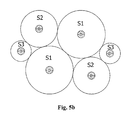
- FIG. 5 a is a longitudinal cross section view of solid state electrochemical cell device where individual battery elements within the bundle has the substrate diameter while the thickness of active layers vary e.g., thickness S 1 >S 2 >S 3 .
- FIG. 5 b is a top view of a solid state electrochemical cell device where individual battery elements within the bundle has the substrate diameter while the thickness of active layers vary e.g., thickness S 1 >S 2 >S 3 .
- FIG. 6 a is a sectioned schematic side view depicting an anode-cathode short of an individual battery element within a bundle.
- FIG. 6 b is a sectioned schematic side view depicting fail-safe battery designs where an individual battery element within a bundle opens at shorted section creating an open circuit allowing other elements of function.
- An embodiment of the present invention relates to using a thermally activated chemical vapor deposition process (TACVD) to nucleate and sequentially grow concentric layers of cathode, electrolyte, anode and anode current collector onto an electrically conductive solid substrate with a circular cross-section.
- the electrically conductive wire substrate acts as a current collector for a first electrochemical electrode, such as for the cathode, during battery charging and discharging.
- deposition of the anode layer onto the electrolyte layer allows outwardly volumetric expansion of anode constituents, for example during the intercalation—deintercalation processes.
- anode as the innermost electrode with the cathode being formed over the electrolyte layer.
- An advantage of concentric layer deposition over a circular substrate is that it minimizes mechanical stress non-uniformities within the deposited material as compared to the planar substrates used in traditional SSBS fabrication.
- the cylindrical structure eliminates the edge effects and stress concentrations common in planar anode structures (i.e., lower compressive stress level in the film stack for the cylindrical geometry as compared to the planar geometry) and thus helps minimize battery capacity fade and maximize battery cycle life.
- the conductive wire substrate may have a circular cross-section characterized by a diameter in a range between 15 ⁇ m and 150 ⁇ m, with a more preferred range between 20 ⁇ m and 40 ⁇ m.
- An (optional) adhesion and reaction/diffusion barrier layer may be formed over the substrate before growing the first electrochemical electrode (either cathode or anode).
- Such a barrier layer may be a metal or alloy material selected, for example, from any one or more of silicon (Si), tungsten (W), titanium (Ti), nickel (Ni), copper (Cu), or iron (Fe). It might also be formed as a reaction product of the wire substrate and first thin-film materials.
- the overlying material layers are composed solid-state materials that can be deposited in a reactor apparatus, either by metal vapor deposition or more preferably by thermally activated chemical vapor deposition. As lithium-ion battery technology develops and new electrochemical reaction systems are developed, or the deposition techniques develop to allow other materials to be deposited, the range of possible layer materials may expand from those currently known.
- the electrochemical active material that composes the cathode layer may be selected from a variety of known materials, including any of various compounds such as LiTiS 2 , LiFeS 2 , LiV 2 O 5 , lithium-doped M x O y , LiMO 2 , LiM 2 O 4 , LiMPO 4 , LiMSiO 4 , where M is any or a combination of the metallic elements selected from nickel (Ni), cobalt (Co), iron (Fe), manganese (Mn), vanadium (V), titanium (Ti) and aluminum (Al), and wherein x>1 and y>1.
- vanadium oxychloride VOCl 3
- oxygen may be used as the reactants.
- Vanadium oxychloride is a liquid at room temperature but is readily vaporized.
- An inert carrier gas such as argon or nitrogen, may be used with the vaporized reactant carrier.
- Lithium tert-butoxide (LiOC(CH 3 ) 3 ) powder that is sublimated may be used as the lithium source for the cathode.
- cobalt(III) acetylacetonate and oxygen may be used, along the aforementioned lithium tert-butoxide.
- triethyl phosphine ((CH 3 CH 2 ) 3 P) and an iron-containing precursor such as bis(cyclo-pentadienyl) iron can be used.
- Ion exchange material for the solid-state electrolyte layer may comprise, for example, any of LiTiS 2 , LiSiS 2 , Li 2 PO 2 N, LiBH 4 and LiBH 4 N, or indeed any solid-state ion exchange material having a room temperature ionic conductivity greater than 5 ⁇ 10 ⁇ 7 S/cm.
- the titanium or silicon precursors may comprise titanium tetrachloride or dichlorosilane, or another silane variant, while tetrabutyl disulfide may be used as the sulfur source and phosphoryl chloride (O:PCl 3 ) as the phosphorus source, together with inert carrier gas or reactant gas such as oxygen.
- phosphoryl chloride O:PCl 3
- triethyl phosphate carried by nitrogen may be used as the reactant.
- the lithium source may be the same lithium tert-butoxide used as precursor in the formation of the cathode.
- the electrochemical active material that composes the anode layer may be selected from a variety of known lithium-receptive materials, including any of carbon (C), silicon (Si), SiC, TiS 2 , V 2 O 5 , germanium (Ge), tin (Sn), antimony (Sb), bismuth (Bi), aluminum (Al), zinc (Zn) and silver (Ag).
- the anode may be a composite microstructure, e.g. of one or more pairs of alternating layers, at least one layer of each pair being the aforementioned lithium-receptive active material and the other at least functioning as a compliant layer, e.g. of boron (B) or carbon (C), that absorbs volume-induced stresses.
- the compliant layer may also be electrochemically active.
- the anode may be composed of lithium metal.
- the individual layers in such a composite anode microstructure may have thicknesses in a range between 10 nm and 5 ⁇ m, and there may be up to about 10 pairs of alternating layers. Additionally, the anode microstructure layers may be formed as any of dense, porous, spherical or nanowire microstructures over the corresponding compliant layers.
- precursors containing silicon such as dichlorosilane (SiCl 2 H 2 ) or silane (SiH 4 ), and precursors containing carbon such as cyclohexane, acetylene or methyl acetylene, or precursors containing both carbon and silicon, such as methylsilane or tetramethylsilane, may be used.
- the thicknesses of the respective thin films that form the active electrode layers (cathode and anode) and the intermediate electrolyte layer may be selected to obtain a specified charge-discharge rate for the electrochemical cell, as well as to obtain a specified ratio of cathode-to-anode capacity.
- the outer current collector may be selected from a variety of conductive materials, including, for example, any of titanium (Ti), germanium (Ge), copper (Cu), aluminum (Al), tungsten (W), a silicide or carbide thereof, or even a conductive polymer.
- conductive materials including, for example, any of titanium (Ti), germanium (Ge), copper (Cu), aluminum (Al), tungsten (W), a silicide or carbide thereof, or even a conductive polymer.
- aluminum collectors aluminum tetrachloride or tributyl aluminum may be used as reactant precursors.
- tungsten silicide based current collectors a combination of tungsten hexafluoride and silane may be used.
- the cell as a whole should, ideally have a circular cross-section (for minimum stresses and absence of edge effects) and a length-to-diameter aspect ratio in excess of 4000:1.
- the vertical TACVD tubular deposition apparatus has a circular cross section with internal diameter ranging from 5 mm to 100 mm, FIG. 1 .
- the substrate is continuously drawn through the multiple section deposition chambers 21 - 29 .
- a wire supply spool 11 holds the bare conductive wire substrate and a motor-driven take-up spool 13 at the other end of the reactor receives the wire after the various thin-film layers have been deposited.
- a tensioner 15 may be provided to keep the wire taut as it passes through the reactor.
- the unique design features of the reactor e.g. small diameter and continuously moving substrate) reduce defects and increases deposit uniformity as flow effects are minimized. This level of uniformity is not possible with traditional physical, chemical, sol-gel or spray deposition methods.
- a thin film is formed consisting of concentric layers in intimate contact.
- FIG. 2 depicts a continuous electrically conductive substrate moving through the deposition chamber(s) 21 - 29 .
- the substrate is heated by passing electrical current through the substrate.
- the deposition apparatus may have a pair of electrical contacts 17 and 18 that are positioned for contact with the conductive wire substrate between the reactor and respective wire supply and take-up spools 11 and 13 .
- the desired temperature range is controlled by varying the current through the substrate as well as varying the amount of cooling gases introduced within each section of reactor and ranges from 300 to 1000 degree Celsius, although for the desired diffusion-limited deposition, a preferred temperature range is between 400 and 800 degree Celsius.
- a long tubular CVD apparatus gives high precursor consumption and high film growth rates.
- Precursor gases supplied through inlet ports 19 are adsorbed onto the heated substrate and cracked via thermal energy.
- the desired component is deposited as a solid onto the wire, while unwanted components are desorbed and pumped out as a gas.
- the precursor compounds thermally decompose at pressures ranging from 5-500 torr.
- the thickness of the each deposited layer can be controlled by varying the length of each reactor section (typically 10 to 190 cm) and the speed of the moving substrate (typically 2 meter/minute to 200 meter/minute).
- Exhaust gasses are pumped through ports 20 , with port maintaining separation of atmosphere between chambers. The reaction is thus envisioned as starting with an input reactant, with diffusion of gas to the wire and absorption of gas onto the wire, where the chemically reaction occurs, then desorption of byproducts and diffusion out as exhaust gas.
- a CVD reactor with up to 15 sections is envisioned in order to deposit the multiple cathode, electrolyte, anode and current collector layers required for an optimized electrochemical cell.
- Different sections 21 - 29 of the reactor for the different layers may be separated by using an argon curtain.
- Argon gas is pumped in at the boundaries of the reactor chamber sections and evacuated after flowing across the reactor. Physical separators could also be used, provided they don't interfere with the drawing of coated wire through the successive sections.
- Tensioners 15 may be used to control the tension of the wire and the substrate feed and collected on reels 11 and 13 .
- a differential pressure and argon curtain or vacuum chamber based mechanism is used to provide atmospheric isolation of reaction chamber.
- Film thicknesses may be monitored by in situ laser measurement using a He—Ne laser and observing interference fringes from incident light reflecting off of the film surface and underlying surfaces.
- Post-deposition film thicknesses may be checked after the wire leaves the reactor using a micrometer or automatically using lasers, and deposition parameters of the reactor sections adjusted as needed. Film thickness is controlled by varying wire speed, reactor temperature, pressure and gas flow rates, reactant/inert gas mixtures and the like.
- the lengths of the various chamber sections are also designed in advance to obtain approximate deposition thicknesses of various layers, with the aforementioned other parameters being adjustable in process. In general, deposition rates and therefore resulting film thicknesses, increase with increasing temperature due to more thermal energy. If the deposition process is diffusion-limited (which is temperature dependent), decreasing the speed of the wire through the reactor should also thicken the coatings due to more time in the reactor.
- Electrodes may be scaled on several levels. First, the capacity for a given length of “wire” may be increased by increasing the thickness of the electrodes. However, there is a limit to the electrode thickness that is determined by the electronic and ionic conductivities and ionic diffusivities in the electrode matrix. Next, the capacity can be increased by simply increasing the length of the wire.
- the wire may be fabricated into various geometries, such as woven into a cloth or wound onto a spool.
- the positive and negative electrodes of a manufactured electrochemical cell may be tested in “puck” or pouch cells using a galvanostatic or constant current cycling method.
- Wire coated with a single electrode component (either cathode or anode) is carefully wrapped around a stainless steel wafer so that the wire forms a continuous mat across the wafer.
- the wire and wafer are then paired with a commercial counter electrode (usually lithium foil).
- the test cell also includes LiPF 6 electrolyte, separator, and a spring to apply pressure and achieve good contact.
- the mass of the active material is estimated through the density and thickness of the coating in order to determine the current at which the desired C-rate can be achieved.
- Typical C-rates of 1C, C/2, C/5 and C/10 are used to test rate capability of the electrode materials.
- the deposition process results in the continuous deposition of cathode, electrolyte, anode and current collector layers along the length of substrate without any provision for the electrical connections required for a functioning electrochemical cell.
- a unique method is presented that allows removal of deposited material exposing the substrate underneath at desired locations 31 (see FIG. 2 ). This allows attachment of electrical connections to the conductive substrate and fabrication of an electrochemical cell of the desired length.
- the thin film solid state battery consist of length to diameter ratio (L:D) greater than 4000:1. This is achieved by modifying the surface energy and chemistry of the substrate at selected locations such that coating does not adhere (bond) to the substrate.
- the surface energy of the substrate at the desired locations can be modified with traditional methods such as sand blasting to impart a tensile stress state or applying an evaporative dye.
- the distance between the debonded or exposed section along the length of the substrate can vary as per the required electrode length.
- a unique solid state electrochemical cell (see FIG. 3 ) is formed by sequentially depositing concentric layers onto the conductive wire substrate 1 consisting of an (optional) adhesion/reaction barrier 2 , a positive electrode or cathode 3 , a solid state electrolyte 4 , a negative electrode or anode 5 , and outermost current collector 6 .
- the electrolyte layer 4 performs both as an ion conductor and an electronic insulator between the positive and negative electrodes 3 and 5 .
- the cathode is formed first, while the anode is the outermost electrode.
- the anode may be formed first, while the cathode would then form the outermost of the two electrodes.
- the concentric layers of active component of solid state Li-ion battery is formed onto an electrically conductive substrate using the following steps:
- the negative electrode component 5 of a solid state Li-ion battery consisting of multiple layers is formed over electrolyte layer 4 using traditional carbon and silicon precursors using the following process steps:
- This unique solid state battery fabrication method offers the advantages of facile and reliable manufacturing processes and improved functional capability compared to traditional flat substrate based battery manufacturing methods.
- the resulting electrochemical cell shown by way of example in FIG. 4 a , comprises positive and negative electrodes (cathode and anode) 43 and 47 which store electrochemical energy, and other elements such as current collectors 41 and 49 , and electrolyte 45 , as well as separators, external terminals and packaging. Note that the anode and cathode positions can be reversed.
- a battery is an assembly of cells in series and parallel configuration to obtain the voltage and Ah capacity requirement for a given application.
- the battery voltage is equal to the cell voltage times the number of cells in series, while the battery capacity is equal to the cell capacity times the number of cells in parallel.
- one example of a battery may be assembled by connecting together the wire substrates of multiple cells and likewise their corresponding outer current collectors to assemble those cells in parallel, as seen for example in FIG. 4 a , and then connect multiple versions of such assemblies in series to obtain the required voltage.
- hundreds of low capacity battery elements are assembled together where negative current collectors 49 of individual battery elements are in electrical contact and connected to an electric terminal while the exposed substrates (i.e., positive current collectors) 41 of the individual battery elements at both ends are connected to second electric terminal ( FIG. 4 a ).
- one hundred individual battery elements each with 1 mAh energy density maybe connected as per FIG. 4 a to create a single bundle (bundle-A) with a capacity of 100 mAh.
- Ten of these individual 100 mAh battery bundle-A are then further connected in parallel to create a 1 Ah battery, FIG. 4 b .
- 1 Ah bundles can be connected in series.
- the modular nature of assembling bundles provides the capability to optimize cell design on multiple parameters simultaneously by varying the diameter D of the wire substrate 51 , thin-film coating thicknesses S 1 , S 2 , S 3 , and thin-film coating structures.
- the proposed assembling method allows use of multiple thickness of active component 53 resulting in a cascading power output with thinner battery element discharging more rapidly than thicker battery element.
- this invention enables assembly of various combinations of individual battery elements allowing a nearly infinite capability to tune capacity and charge-discharge rates for specific applications.
- the local increase in current density causes a rapid increase in the temperature of the substrate of the shorted electrochemical cell within the bundle, resulting in instantaneously melting of the substrate in the proximity of the short.
- the low resistance electrical path between the positive and negative electrode i.e. the short
- the rest of the battery elements will continue to function although with reduced capacity.
- the current carrying capacity (ampacity) of the substrate of individual battery element within the bundle, diameter of the substrate and the energy density or capacity of a electrochemical cell are critical factors that can be adjusted to utilize the teachings of this invention top make electrochemical cell as fail-safe device.
Landscapes
- Chemical & Material Sciences (AREA)
- Chemical Kinetics & Catalysis (AREA)
- General Chemical & Material Sciences (AREA)
- Engineering & Computer Science (AREA)
- Electrochemistry (AREA)
- Materials Engineering (AREA)
- Manufacturing & Machinery (AREA)
- Organic Chemistry (AREA)
- Metallurgy (AREA)
- Mechanical Engineering (AREA)
- Inorganic Chemistry (AREA)
- Physics & Mathematics (AREA)
- Condensed Matter Physics & Semiconductors (AREA)
- General Physics & Mathematics (AREA)
- Composite Materials (AREA)
- Secondary Cells (AREA)
- Battery Electrode And Active Subsutance (AREA)
Abstract
Description
- 1. Modification of the surface energy of the substrate at selected locations along the length prior to entering the deposition section of the reactor (e.g. in cleaning chamber 21);
- 2. Resistive heating of the substrate and etching of the native oxide (if any);
- 3. (Optional) Nucleation and concentric growth (in deposition chamber section 22) of an electrically conductive thin layer on to the heated substrate serving the purpose of providing an adhesion layer (bonding layer) and a reaction and diffusion barrier function between the substrate and the subsequent coating;
- 4. Nucleation and concentric growth (in deposition chamber section 23) of a positive electrode layer onto the bond layer (or directly onto the substrate if the bonding layer is not used);
- 5. An optional in-situ elevated thermal annealing of deposited positive electrode (in annealing chamber section 24) to produce the desired crystal structure or chemical composition (in this example, the positive electrode or cathode is grown inside the electrolyte layer and the negative electrode or anode);
- 6. Nucleation and concentric growth (in deposition chamber section 25) of an electrolyte layer electrode onto the positive electrode layer;
- 7. Nucleation and concentric growth (in multiple deposition chamber sections 27) of the negative electrode onto the electrolyte layer (here the anode is the outer of the two electrodes);
- 8. Deposition (in chamber 29) of a negative electrode current collector electrode onto the anode using precursors of conductive metals or alloys of elements such as Al, Ag, Ti, Cu, or W (note: this outermost layer also functions as a hermetically sealing layer);
- 9. Debonding of deposited coating from the substrate at selected location during cool down at the exit section of reactor exposing the substrate; and
- 10. Sectioning of the coated substrate at exposed sections to create a solid state battery. We define such battery as “individual battery element”.
- 1. Modification of the surface energy of the substrate at selected locations along the length prior to entering the
multi-section deposition chamber 27 ofFIG. 1 ; - 2. Resistively heating of substrate and hydrogen etching of the native oxide (if any) in
reactor section 1; - 3. Nucleation and concentric growth of an electrically conductive thin layer in
reactor section 2 on to the heated substrate serving the purpose of providing an adhesion layer (bonding layer) and a reaction and diffusion barrier function between the substrate and the subsequent coating (optional); - 4. Nucleation and concentric growth of positive electrode layer onto the bond layer (or onto the substrate), in
reactor section 3; - 5. An optional in-situ elevated thermal annealing of deposited positive electrode to induce desired level of crystallization in oxygen or desired environment, in
reactor section 4; - 6. Nucleation and concentric growth of ion exchanging electrolyte layer electrode onto the positive electrode layer,
reactor section 5; - 7. Nucleation and concentric growth of multilayer silicon-carbon based negative electrode on to the electrolyte layer using the following sub-steps and depicted in
FIG. 3 (note: as before, steps 4-5 and 7 may be reversed such that the anode microstructure is formed first, while the cathode forms the outer electrode):- a. Deposition of the carbon layer serving both as stress compliant layer as well active material layer capable of intercalating-deintercalating;
- b. Deposition of the silicon layer serving function of an active material layer capable of intercalating-deintercalating;
- c. Repeat step 7-8 in subsequent sections of reactor to create multilayer negative electrode structure as required by application consisting of alternating layers of silicon and carbon; and
- d. Final deposition of a carbon layer serving function of reaction barrier between silicon and top current collector;
- 8. Debonding of deposited coating from the substrate at selected location during cool down at the exit section of reactor exposing the substrate;
- 9. Sectioning of coated substrate at exposed section to create a solid state battery with aspect ratio greater than 4000:1. We define such battery as “individual battery element”.
Claims (20)
Priority Applications (1)
| Application Number | Priority Date | Filing Date | Title |
|---|---|---|---|
| US14/593,797 US10221485B2 (en) | 2014-01-09 | 2015-01-09 | High energy density solid state lithium ion battery with fail-safe |
Applications Claiming Priority (2)
| Application Number | Priority Date | Filing Date | Title |
|---|---|---|---|
| US201461925528P | 2014-01-09 | 2014-01-09 | |
| US14/593,797 US10221485B2 (en) | 2014-01-09 | 2015-01-09 | High energy density solid state lithium ion battery with fail-safe |
Publications (2)
| Publication Number | Publication Date |
|---|---|
| US20150221973A1 US20150221973A1 (en) | 2015-08-06 |
| US10221485B2 true US10221485B2 (en) | 2019-03-05 |
Family
ID=53755579
Family Applications (1)
| Application Number | Title | Priority Date | Filing Date |
|---|---|---|---|
| US14/593,797 Expired - Fee Related US10221485B2 (en) | 2014-01-09 | 2015-01-09 | High energy density solid state lithium ion battery with fail-safe |
Country Status (1)
| Country | Link |
|---|---|
| US (1) | US10221485B2 (en) |
Families Citing this family (5)
| Publication number | Priority date | Publication date | Assignee | Title |
|---|---|---|---|---|
| US11121409B2 (en) * | 2019-05-08 | 2021-09-14 | International Business Machines Corporation | Electrochemical energy storage |
| JP2023507160A (en) | 2019-12-20 | 2023-02-21 | シオン・パワー・コーポレーション | lithium metal electrode |
| US11731160B2 (en) | 2020-07-20 | 2023-08-22 | Rivian Ip Holdings, Llc | Systems and methods for managing sharp transitions for powder coating |
| CN113675403A (en) * | 2021-07-30 | 2021-11-19 | 华南师范大学 | Solid-state battery and preparation method and application thereof |
| CN113611969B (en) * | 2021-08-03 | 2023-02-28 | 东南大学 | Encapsulation and preparation method of a solid-state lithium-ion battery |
Citations (11)
| Publication number | Priority date | Publication date | Assignee | Title |
|---|---|---|---|---|
| US2734478A (en) | 1956-02-14 | Copper | ||
| US3542604A (en) | 1965-02-24 | 1970-11-24 | Mc Donnell Douglas Corp | Thermal battery |
| US3562002A (en) | 1968-04-24 | 1971-02-09 | Air Reduction | Method and apparatus for vapor deposition |
| US20030068559A1 (en) * | 2001-09-12 | 2003-04-10 | Armstrong Joseph H. | Apparatus and method for the design and manufacture of multifunctional composite materials with power integration |
| US7351449B2 (en) | 2000-09-22 | 2008-04-01 | N Gimat Co. | Chemical vapor deposition methods for making powders and coatings, and coatings made using these methods |
| US20080268343A1 (en) | 2007-04-27 | 2008-10-30 | Toshitada Sato | Electrochemical element and electrode thereof, method and apparatus for manufacturing the electrode, method and apparatus for lithiation treatment |
| US7717968B2 (en) | 2006-03-08 | 2010-05-18 | Yevgen Kalynushkin | Electrode for energy storage device and method of forming the same |
| JP2010129412A (en) * | 2008-11-28 | 2010-06-10 | Seiko Epson Corp | Electrochemical device |
| US20100261071A1 (en) * | 2009-04-13 | 2010-10-14 | Applied Materials, Inc. | Metallized fibers for electrochemical energy storage |
| US20140178753A1 (en) * | 2012-12-24 | 2014-06-26 | Industrial Technology Research Institute | Lithium ion battery and electrode structure thereof |
| US8993172B2 (en) | 2011-12-10 | 2015-03-31 | Kalptree Energy, Inc. | Li-ion battery and battery active components on metal wire |
-
2015
- 2015-01-09 US US14/593,797 patent/US10221485B2/en not_active Expired - Fee Related
Patent Citations (11)
| Publication number | Priority date | Publication date | Assignee | Title |
|---|---|---|---|---|
| US2734478A (en) | 1956-02-14 | Copper | ||
| US3542604A (en) | 1965-02-24 | 1970-11-24 | Mc Donnell Douglas Corp | Thermal battery |
| US3562002A (en) | 1968-04-24 | 1971-02-09 | Air Reduction | Method and apparatus for vapor deposition |
| US7351449B2 (en) | 2000-09-22 | 2008-04-01 | N Gimat Co. | Chemical vapor deposition methods for making powders and coatings, and coatings made using these methods |
| US20030068559A1 (en) * | 2001-09-12 | 2003-04-10 | Armstrong Joseph H. | Apparatus and method for the design and manufacture of multifunctional composite materials with power integration |
| US7717968B2 (en) | 2006-03-08 | 2010-05-18 | Yevgen Kalynushkin | Electrode for energy storage device and method of forming the same |
| US20080268343A1 (en) | 2007-04-27 | 2008-10-30 | Toshitada Sato | Electrochemical element and electrode thereof, method and apparatus for manufacturing the electrode, method and apparatus for lithiation treatment |
| JP2010129412A (en) * | 2008-11-28 | 2010-06-10 | Seiko Epson Corp | Electrochemical device |
| US20100261071A1 (en) * | 2009-04-13 | 2010-10-14 | Applied Materials, Inc. | Metallized fibers for electrochemical energy storage |
| US8993172B2 (en) | 2011-12-10 | 2015-03-31 | Kalptree Energy, Inc. | Li-ion battery and battery active components on metal wire |
| US20140178753A1 (en) * | 2012-12-24 | 2014-06-26 | Industrial Technology Research Institute | Lithium ion battery and electrode structure thereof |
Non-Patent Citations (1)
| Title |
|---|
| Printout: E.F. Vaage, "Transmission Properties of Laminated Clogston Type Conductor", Manuscript Dec. 8, 1952, pp. 695-713. |
Also Published As
| Publication number | Publication date |
|---|---|
| US20150221973A1 (en) | 2015-08-06 |
Similar Documents
| Publication | Publication Date | Title |
|---|---|---|
| US9559380B2 (en) | Li-ion battery and battery active components on metal wire | |
| Du et al. | Recent advances in the interface engineering of solid-state Li-ion batteries with artificial buffer layers: challenges, materials, construction, and characterization | |
| US12355072B2 (en) | Multilayer anodes for lithium-based energy storage devices | |
| US8956761B2 (en) | Lithium ion battery and method for manufacturing of such battery | |
| JP6770952B2 (en) | Protective layer in lithium-ion electrochemical cells, and related electrodes and methods | |
| US10221485B2 (en) | High energy density solid state lithium ion battery with fail-safe | |
| CN109643784B (en) | Lithium borosilicate glass as electrolyte and electrode protection layer | |
| CA2776980C (en) | Nano-structured lithium-sulfur battery and method of making same | |
| US8551656B2 (en) | Solid electrolyte cell and positive electrode active material | |
| US12191501B2 (en) | Anodes for lithium-based energy storage devices | |
| US12136726B2 (en) | Asymmetric anodes for lithium-based energy storage devices | |
| JP4850405B2 (en) | Lithium ion secondary battery and manufacturing method thereof | |
| JP2016505093A (en) | Method for forming at least one layer of film for solid phase thin film battery, plasma powder injection apparatus used for the film forming method, and solid phase thin film battery | |
| CN110870122B (en) | Thin-film lithium-ion battery with fast charging speed | |
| CN108780875B (en) | Secondary battery | |
| JP6015297B2 (en) | Lithium ion secondary battery | |
| CN115210902A (en) | Method | |
| XIA et al. | Amorphous LiSiON Thin Film Electrolyte | |
| HK1156369A (en) | High volume manufacture of electrochecmicals cells using physical vapor deposition |
Legal Events
| Date | Code | Title | Description |
|---|---|---|---|
| AS | Assignment |
Owner name: KALPTREE ENERGY, INC., CALIFORNIA Free format text: ASSIGNMENT OF ASSIGNORS INTEREST;ASSIGNORS:UPADHYAYA, DEEPAK;ISAACSON, MARK J.;REEL/FRAME:034676/0518 Effective date: 20150109 |
|
| AS | Assignment |
Owner name: ADAVOLT, INC., CALIFORNIA Free format text: CHANGE OF NAME;ASSIGNOR:KALPTREE ENERGY, INC.;REEL/FRAME:048008/0599 Effective date: 20180327 |
|
| STCF | Information on status: patent grant |
Free format text: PATENTED CASE |
|
| FEPP | Fee payment procedure |
Free format text: MAINTENANCE FEE REMINDER MAILED (ORIGINAL EVENT CODE: REM.); ENTITY STATUS OF PATENT OWNER: SMALL ENTITY |
|
| LAPS | Lapse for failure to pay maintenance fees |
Free format text: PATENT EXPIRED FOR FAILURE TO PAY MAINTENANCE FEES (ORIGINAL EVENT CODE: EXP.); ENTITY STATUS OF PATENT OWNER: SMALL ENTITY |
|
| STCH | Information on status: patent discontinuation |
Free format text: PATENT EXPIRED DUE TO NONPAYMENT OF MAINTENANCE FEES UNDER 37 CFR 1.362 |
|
| FP | Lapsed due to failure to pay maintenance fee |
Effective date: 20230305 |