US10204852B2 - Circuit substrate and semiconductor package structure - Google Patents
Circuit substrate and semiconductor package structure Download PDFInfo
- Publication number
- US10204852B2 US10204852B2 US15/423,788 US201715423788A US10204852B2 US 10204852 B2 US10204852 B2 US 10204852B2 US 201715423788 A US201715423788 A US 201715423788A US 10204852 B2 US10204852 B2 US 10204852B2
- Authority
- US
- United States
- Prior art keywords
- conductive
- circuit substrate
- conductive line
- chip
- line pattern
- Prior art date
- Legal status (The legal status is an assumption and is not a legal conclusion. Google has not performed a legal analysis and makes no representation as to the accuracy of the status listed.)
- Active
Links
Images


Classifications
-
- H—ELECTRICITY
- H10—SEMICONDUCTOR DEVICES; ELECTRIC SOLID-STATE DEVICES NOT OTHERWISE PROVIDED FOR
- H10W—GENERIC PACKAGES, INTERCONNECTIONS, CONNECTORS OR OTHER CONSTRUCTIONAL DETAILS OF DEVICES COVERED BY CLASS H10
- H10W70/00—Package substrates; Interposers; Redistribution layers [RDL]
- H10W70/60—Insulating or insulated package substrates; Interposers; Redistribution layers
- H10W70/62—Insulating or insulated package substrates; Interposers; Redistribution layers characterised by their interconnections
- H10W70/65—Shapes or dispositions of interconnections
-
- H01L23/49838—
-
- H01L23/13—
-
- H01L23/145—
-
- H01L23/49811—
-
- H01L23/49827—
-
- H01L24/00—
-
- H—ELECTRICITY
- H10—SEMICONDUCTOR DEVICES; ELECTRIC SOLID-STATE DEVICES NOT OTHERWISE PROVIDED FOR
- H10W—GENERIC PACKAGES, INTERCONNECTIONS, CONNECTORS OR OTHER CONSTRUCTIONAL DETAILS OF DEVICES COVERED BY CLASS H10
- H10W70/00—Package substrates; Interposers; Redistribution layers [RDL]
- H10W70/60—Insulating or insulated package substrates; Interposers; Redistribution layers
- H10W70/62—Insulating or insulated package substrates; Interposers; Redistribution layers characterised by their interconnections
- H10W70/63—Vias, e.g. via plugs
- H10W70/635—Through-vias
-
- H—ELECTRICITY
- H10—SEMICONDUCTOR DEVICES; ELECTRIC SOLID-STATE DEVICES NOT OTHERWISE PROVIDED FOR
- H10W—GENERIC PACKAGES, INTERCONNECTIONS, CONNECTORS OR OTHER CONSTRUCTIONAL DETAILS OF DEVICES COVERED BY CLASS H10
- H10W70/00—Package substrates; Interposers; Redistribution layers [RDL]
- H10W70/60—Insulating or insulated package substrates; Interposers; Redistribution layers
- H10W70/67—Insulating or insulated package substrates; Interposers; Redistribution layers characterised by their insulating layers or insulating parts
- H10W70/68—Shapes or dispositions thereof
-
- H—ELECTRICITY
- H10—SEMICONDUCTOR DEVICES; ELECTRIC SOLID-STATE DEVICES NOT OTHERWISE PROVIDED FOR
- H10W—GENERIC PACKAGES, INTERCONNECTIONS, CONNECTORS OR OTHER CONSTRUCTIONAL DETAILS OF DEVICES COVERED BY CLASS H10
- H10W70/00—Package substrates; Interposers; Redistribution layers [RDL]
- H10W70/60—Insulating or insulated package substrates; Interposers; Redistribution layers
- H10W70/67—Insulating or insulated package substrates; Interposers; Redistribution layers characterised by their insulating layers or insulating parts
- H10W70/69—Insulating materials thereof
- H10W70/695—Organic materials
-
- H—ELECTRICITY
- H10—SEMICONDUCTOR DEVICES; ELECTRIC SOLID-STATE DEVICES NOT OTHERWISE PROVIDED FOR
- H10W—GENERIC PACKAGES, INTERCONNECTIONS, CONNECTORS OR OTHER CONSTRUCTIONAL DETAILS OF DEVICES COVERED BY CLASS H10
- H10W72/00—Interconnections or connectors in packages
-
- H—ELECTRICITY
- H10—SEMICONDUCTOR DEVICES; ELECTRIC SOLID-STATE DEVICES NOT OTHERWISE PROVIDED FOR
- H10W—GENERIC PACKAGES, INTERCONNECTIONS, CONNECTORS OR OTHER CONSTRUCTIONAL DETAILS OF DEVICES COVERED BY CLASS H10
- H10W90/00—Package configurations
- H10W90/701—Package configurations characterised by the relative positions of pads or connectors relative to package parts
-
- H01L2224/1308—
-
- H01L2224/81—
-
- H—ELECTRICITY
- H10—SEMICONDUCTOR DEVICES; ELECTRIC SOLID-STATE DEVICES NOT OTHERWISE PROVIDED FOR
- H10W—GENERIC PACKAGES, INTERCONNECTIONS, CONNECTORS OR OTHER CONSTRUCTIONAL DETAILS OF DEVICES COVERED BY CLASS H10
- H10W72/00—Interconnections or connectors in packages
- H10W72/071—Connecting or disconnecting
- H10W72/072—Connecting or disconnecting of bump connectors
-
- H—ELECTRICITY
- H10—SEMICONDUCTOR DEVICES; ELECTRIC SOLID-STATE DEVICES NOT OTHERWISE PROVIDED FOR
- H10W—GENERIC PACKAGES, INTERCONNECTIONS, CONNECTORS OR OTHER CONSTRUCTIONAL DETAILS OF DEVICES COVERED BY CLASS H10
- H10W72/00—Interconnections or connectors in packages
- H10W72/20—Bump connectors, e.g. solder bumps or copper pillars; Dummy bumps; Thermal bumps
- H10W72/221—Structures or relative sizes
- H10W72/222—Multilayered bumps, e.g. a coating on top and side surfaces of a bump core
-
- H—ELECTRICITY
- H10—SEMICONDUCTOR DEVICES; ELECTRIC SOLID-STATE DEVICES NOT OTHERWISE PROVIDED FOR
- H10W—GENERIC PACKAGES, INTERCONNECTIONS, CONNECTORS OR OTHER CONSTRUCTIONAL DETAILS OF DEVICES COVERED BY CLASS H10
- H10W72/00—Interconnections or connectors in packages
- H10W72/20—Bump connectors, e.g. solder bumps or copper pillars; Dummy bumps; Thermal bumps
- H10W72/231—Shapes
- H10W72/232—Plan-view shape, i.e. in top view
-
- H—ELECTRICITY
- H10—SEMICONDUCTOR DEVICES; ELECTRIC SOLID-STATE DEVICES NOT OTHERWISE PROVIDED FOR
- H10W—GENERIC PACKAGES, INTERCONNECTIONS, CONNECTORS OR OTHER CONSTRUCTIONAL DETAILS OF DEVICES COVERED BY CLASS H10
- H10W72/00—Interconnections or connectors in packages
- H10W72/20—Bump connectors, e.g. solder bumps or copper pillars; Dummy bumps; Thermal bumps
- H10W72/241—Dispositions, e.g. layouts
- H10W72/247—Dispositions of multiple bumps
- H10W72/248—Top-view layouts, e.g. mirror arrays
-
- H—ELECTRICITY
- H10—SEMICONDUCTOR DEVICES; ELECTRIC SOLID-STATE DEVICES NOT OTHERWISE PROVIDED FOR
- H10W—GENERIC PACKAGES, INTERCONNECTIONS, CONNECTORS OR OTHER CONSTRUCTIONAL DETAILS OF DEVICES COVERED BY CLASS H10
- H10W72/00—Interconnections or connectors in packages
- H10W72/20—Bump connectors, e.g. solder bumps or copper pillars; Dummy bumps; Thermal bumps
- H10W72/251—Materials
- H10W72/252—Materials comprising solid metals or solid metalloids, e.g. PbSn, Ag or Cu
Definitions
- the present invention relates to a circuit substrate and a semiconductor package structure, and in particular to a circuit substrate and a semiconductor package structure with a high routing density and a high bump density.
- chip carriers are currently used to connect semiconductor integrated circuit (IC) chips to electronic devices in the lower layered-level, for example, circuit boards including motherboards or module boards.
- the circuit boards are usually used as the high pin-count chip carriers.
- the circuit boards are formed by alternately laminating a plurality of patterned conductive layers and a plurality of dielectric layers. Any two of the patterned conductive layers can be electrically connected to each other through conductive vias.
- routing density and the bump density of the circuit boards must be increased to meet the requirements of the integrated multi-chip packages and the multiple input/output (I/O) terminals chips.
- Exemplary embodiments provide a circuit substrate and a semiconductor package structure.
- An exemplary embodiment of a circuit substrate for a chip bonding thereon includes a core substrate having a chip-side surface and a bump-side surface opposite to the chip-side surface, a first through via plug passing through the core substrate, a pad disposed on the bump-side surface, in contact with the first through via plug, and a first thickness enhancing conductive pattern disposed on a surface of the pad, which is away from the bump-side surface.
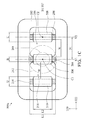
- FIG. 1A is a plan view of a circuit substrate in accordance with one embodiment of the disclosure.
- FIG. 1B is a cross-sectional view of a circuit substrate in accordance with one embodiment of the disclosure.
- FIG. 1C is a schematic view showing the diameters of the elements of a circuit substrate in accordance with one embodiment of the disclosure
- FIG. 2A is a plan view of a circuit substrate in accordance with another embodiment of the disclosure.
- FIG. 2B is a cross-sectional view of a circuit substrate in accordance with another embodiment of the disclosure.
- FIGS. 2C and 2D are schematic views showing the diameters of the elements of a circuit substrate in accordance with another embodiment of the disclosure.
- FIG. 3A is a plan view of a circuit substrate in accordance with yet another embodiment of the disclosure.
- FIG. 3B is a cross-sectional view of a circuit substrate in accordance with yet another embodiment of the disclosure.
- FIG. 3C is a schematic view showing the diameters of the elements of a circuit substrate in accordance with yet another embodiment of the disclosure.
- FIG. 4A is a plan view of a circuit substrate in accordance with still another embodiment of the disclosure.
- FIG. 4B is a cross-sectional view of a circuit substrate in accordance with still another embodiment of the disclosure.
- FIGS. 5A-5F are plan views of thickness enhancing conductive patterns on pads of circuit substrates in accordance with some embodiments of the disclosure.
- FIGS. 5G-5M are three-dimensional views of thickness enhancing conductive patterns on pads of circuit substrates in accordance with some embodiments of the disclosure.
- Embodiments provide a circuit substrate.
- a chip is flipped and bonded on the circuit substrate using the bump-on-trace (BOT) technology.
- BOT bump-on-trace
- one or more conductive line patterns are directly disposed on and directly connecting to a through via plug, which is used to transmit power/ground (GND) signals.
- the conductive line pattern and the through via plug are formed of the same materials, so that the routing density and the bump density are increased.
- the conductive line patterns respectively disposed on adjacent through via plugs may be merged as a single conductive planar pattern with one or more thickness enhancing conductive patterns disposed thereon to increase the bonding strength.
- one or more other thickness enhancing conductive patterns may be disposed on the pad, which connects to the through via plug, to increase the bonding strength between the pad and the bump.
- FIG. 1A is a plan view of a circuit substrate 500 a of a semiconductor package 600 a in accordance with one embodiment of the disclosure.
- FIG. 1B is a cross-sectional view of FIG. 1A .
- FIG. 1C is a schematic view showing the diameters of the elements of the circuit substrate 500 a in accordance with one embodiment of the disclosure.
- FIGS. 1A and 1C show conductive pillars of chips but do not show the substrate and solder bumps for conveniently illustrating the arrangement of the circuit substrate.
- the circuit substrate 500 a in accordance with one embodiment of the disclosure comprises a core substrate 200 , a through via plug 204 , conductive line patterns 206 , 208 and 210 , and a pad 212 .
- the core substrate 200 has a chip-side surface 201 and a bump-side surface 203 opposite to the chip-side surface 201 .
- the core substrate 200 may be formed of paper phenolic resin, composite epoxy, polyimide resin or composite materials, which include BT (Bismaleimide-Triazine) resin or reinforced resins including glass fibers.
- the bump-side surface 203 may serve as a ball-side surface.
- the through via plug 204 is formed through the core substrate 200 , and two terminals of the through via plug 204 are aligned the chip-side surface 201 and the bump-side surface 203 of the core substrate 200 . Additionally, the through via plug 204 is arranged between the adjacent conductive line patterns 208 and 210 . In this embodiment, the through via plug 204 is arranged corresponding to the pad 212 . In other words, the conductive line pattern 206 , the through via plug 204 and the pad 212 overlap one another in a top view ( FIG. 1A ). The pad 212 connects with the electronic devices, which is positioned in the lower layered-level, by the solder bumps or solder balls (not shown).
- the through via plug 204 is used to transmit power voltage supply and ground (GND) voltage supply, but not to transmit digital signals.
- the through via plug 204 may be formed of conductive metals including copper or copper alloy.
- the through via plug 204 may be formed by the laser drilling process and the electronic plating process.
- the conductive line patterns 206 , 208 and 210 separated from one another are disposed on the chip-side surface 201 of the core substrate 200 , respectively.
- the pad 212 is disposed on the bump-side surface 203 of the core substrate 200 .
- the conductive line patterns 206 , 208 and 210 are specially indicated as bonding segments of the conductive lines.
- the bonding segments are merely small line segments of the conductive lines, respectively.
- the thickness of the bonding segments is the same as that of the conductive lines used to form the bonding segments.
- the conductive line patterns 206 , 208 and 210 and the pad 212 may be formed of conductive metals including copper or copper alloy.
- a conductive layer is entirely formed on the chip-side surface 201 and the bump-side surface 203 of the core substrate 200 by performing the electronic plating process, the laminating process and the coating process.
- the image transfer process which includes the photoresist coating, developing, etching and stripping processes, is performed to form the conductive line patterns 206 , 208 and 210 on the chip-side surface 201 , and the pad 212 on the bump-side surface 203 .
- conductive planar layers 202 and 211 for example, copper layers, are respectively formed on the chip-side surface 201 and the bump-side surface 203 of the core substrate 200 during forming the conductive line patterns 206 , 208 and 210 and the pad 212 .
- the conductive line patterns 206 , 208 and 210 and the conductive planar layer 202 belong to the same layered-level.
- the pad 212 and the conductive planar layer 211 belong to the same layered-level.
- the conductive line pattern 206 may be electrically connected to the conductive line pattern 208 and/or the conductive line pattern 210 through the conductive planar layer 202 .
- the conductive line patterns 206 , 208 and 210 may be used to transmit the same voltage supply, such as power voltage supply or ground (GND) voltage supply, but not to transmit digital signals. As shown in FIG.
- FIG. 1A the conductive line patterns 206 , 208 and 210 and the conductive planar layer 202 , which surrounds the conductive line patterns 206 and 210 and connects to the conductive line pattern 208 , collectively from vent holes 216 and 218 on the chip-side surface 201 of the core substrate 200 .
- Different portions of the through via plug 204 are exposed at the vent holes 216 and 218 , respectively.
- the shape of the vent holes 216 and 218 may include a rectangular shape, a polygonal shape or an elliptical shape. Therefore, FIG. 1B may serve as a cross-sectional view of FIG. 1A along the width direction (the second direction 322 ) of the conductive line patterns 206 , 208 and 210 of the circuit substrate 500 a.
- the conductive line pattern 206 is designed to be a BOT conductive line pattern which directly connects to the through via plug 204 .
- the second direction 322 is defined as a direction substantially parallel to the width direction of the BOT conductive line pattern (i.e. the conductive line pattern 206 ), which directly connects to the through via plug.
- the first direction 320 is defined as a direction substantially parallel to the length direction of the conductive line pattern 206 . As shown in FIG.
- the width of the vent holes 216 and 218 along the second direction 322 is defined as W
- the length of the vent holes 216 and 218 along the first direction 320 is defined as L 1 , according to the definition of the second direction 322 and the first direction 320 . Therefore, the through via plug 204 is in direct contact with the conductive line pattern 206 , and partially overlapping the conductive line pattern 206 . Also, the through via plug 204 is not in direct contact with the conductive line patterns 208 and 210 .
- the conductive line patterns 206 , 208 and 210 may be designed to have the same width B (the minimum width of the conductive line defined by the design rule). The width B is less than or equal to the diameter D 1 of the through via plug 204 . Additionally, the width B of the conductive line patterns 206 , 208 and 210 are less than or equal to the width W of the vent holes 216 and 218 along the second direction 322 ( FIG. 1C ).
- the circuit substrate 500 a can be a two-layer circuit board. In other embodiments, the number of conductive layers on the chip-side surface 201 is different from that on the bump-side surface 203 of the core substrate 200 . Therefore, the circuit substrate 500 a can be a single-side build-up circuit substrate.
- the semiconductor package 600 a further comprises solder mask layers 215 and 214 on the chip-side surface 201 and the bump-side surface 203 of the core substrate 200 , respectively.
- the solder mask layer 215 having one or more openings covers a portion of the conductive planar layer 202 . Portions of the conductive line patterns 206 , 208 and 210 are exposed at the openings of the solder mask layer 215 . Also, the openings are separated from the conductive line patterns 206 , 208 and 210 by a distance.
- the solder mask layer 215 may prevent the underlying conductive planar layer 202 from oxidation.
- the solder mask layer 214 may have one or more openings to expose the pad 212 .
- the openings of the solder mask layer 214 are separated from the pad 212 by a distance.
- the openings are separated from separated from the pad 212 to prevent solder bumps 240 disposed on the pad 212 from short-circuiting with other conductive lines and solder bumps.
- the openings of the solder mask layer 214 may provide positions of the subsequent conductive bumps.
- the solder mask layers 214 and 215 may comprise solder-resistant materials including solder mask, or insulating materials including polyimide, ajinomoto build-up film, epoxy, polymethylmethacrylate (PMMA) resin, a composite including epoxy and PMMA resin, or polypropylene (PP).
- the solder mask layers 214 and 215 may be formed by a coating, a printing process, an adhesion process, a laminating process or other proper processes.
- the semiconductor package 600 a further comprises a solder bump 240 disposed on the pad 212 .
- the solder bump 240 may be formed of materials including a solder paste.
- the solder bump 240 may be formed on the pad 212 by a deposition process and a patterning process, or printing process/ball attachment process.
- FIGS. 1A-1C illustrate the relationship between a chip 300 a and the circuit substrate 500 a bonded thereto.
- the chip 300 a includes a substrate 302 (for example, a silicon substrate), conductive pillars 306 , 308 and 310 , and solder bumps 312 , 314 and 316 .
- the chip 300 a is flipped up-side-down by the flip-chip process, so that the conductive pillars 306 , 308 and 310 on a top surface 304 of the substrate 302 are electrically connected to the conductive line patterns 206 , 208 and 210 , respectively.
- the conductive pillar 306 may be electrically connected to the through via plug 204 and the pad 212 by the conductive line pattern 206 . That is to say, the conductive line pattern 206 partially overlaps the through via plug 204 , the pad 212 and conductive pillar 306 ( FIGS. 1A-1C ).
- the conductive pillars 306 , 308 and 310 have a width U along the second direction 322 and a length L 2 along the first direction 320 .
- the width U is not smaller than the width B of the conductive line patterns; the length L 2 of the conductive pillars is not larger than the length L 1 of the conductive line patterns.
- the conductive pillars 306 , 308 and 310 may be formed of copper.
- the materials and the formation of the solder bumps 312 , 314 and 316 may be the same as or similar to those of the solder bump 240 .
- the conductive line pattern 206 is designed not to be disposed on the through via plug 204 in the conventional technology, the chip 300 a is designed without including the arrangement of the conductive pillar 306 and the solder bump 312 .
- the circuit substrate 500 a is designed to dispose the conductive line pattern 206 on the through via plug 204 , and thus the density of the conductive pillars disposed on the chip 300 a is increased.
- FIG. 1C illustrates the relationship between the diameters of the elements (for example, the conductive line patterns 206 , 208 and 210 and the vent holes 216 and 218 ) of a circuit substrate 500 a and the diameters of the conductive pillars 306 , 308 and 310 of the chip 300 a in the semiconductor package 600 a in accordance with one embodiment of the disclosure.
- the conductive line pattern 206 which is directly disposed on the through via plug 204 , and the conductive line pattern 208 (or 210 ) adjacent thereto are extended substantially along the first direction 320 , and separated from each other substantially along the second direction 322 perpendicular to the first direction 320 .
- Equation (1) B ⁇ D 1, and B ⁇ W Equation (1)
- B is the width of the conductive line pattern 206 and the conductive line pattern 208 (or 210 ) along the second direction 322
- D 1 is the diameter of the through via plug 204
- W is the width of the vent holes 216 (or 218 ) along the second direction 322 .
- the position of the conductive line pattern 208 (or 210 ) is shifted, for example, if an extension line H 1 ′ passing through the centers of the conductive line pattern 206 and the conductive line pattern 208 (or 210 ) is not parallel to the second direction 322 , the angle ⁇ between the first extension line H 1 along the second direction 322 and passing through the first center point C 1 of the conductive line pattern 206 , and a second extension line H 1 ′ passing through the first center point C 1 and the second center point C 2 of the conductive line pattern 208 (or 210 ), satisfy the Equation (2): 0° ⁇ 45° Equation (2)
- the angle ⁇ is equal to zero degrees.
- B is the width of the conductive line pattern 206 and the width of the conductive line pattern 208 (or 210 ) along the second direction 322
- U is the width of the conductive pillars 306 , 308 and 310 along the second direction 322 .
- an angle ⁇ between a first extension line V 1 along the first direction 320 and passing through the first center point C 1 of the conductive line pattern 206 , which is directly disposed on the through via plug 204 , and a second extension line V 2 passing through the second center point C 2 of the adjacent conductive line pattern 208 (or 210 ) satisfies Equation (4): 0° ⁇ 90° Equation (4)
- the angle ⁇ is equal to zero degrees.
- FIG. 2A is a plan view of a circuit substrate 500 b of a semiconductor package 600 b in accordance with one embodiment of the disclosure.
- FIG. 2B is a cross-sectional view of FIG. 2A .
- FIG. 2B may serve as a cross-sectional view along the width direction (the second direction 322 ) of the BOT conductive line pattern (for example, the conductive line pattern 206 ), which directly connects to the through via plug, of the circuit substrate 500 b .
- FIGS. 2C and 2 D are schematic views showing the diameters of the elements of the circuit substrate 500 b and conductive pillars of a chip in accordance with one embodiment of the disclosure.
- FIGS. 1A-1C show the conductive pillars of the chip but do not show the substrate and solder bumps for conveniently illustrating the arrangement of the circuit substrate 500 b .
- the conductive planar layer 202 may have segments 202 a and 202 b .
- the segment 202 a is disposed between the conductive line pattern 206 , which is directly disposed on the through via plug 204 , and the adjacent conductive line pattern 208 .
- the segment 202 a is substantially parallel to the conductive line pattern 206 .
- the segment 202 b is disposed between the conductive line pattern 206 , which is directly disposed on the through via plug 204 , and the adjacent conductive line pattern 210 .
- the segment 202 b is substantially parallel to the conductive line pattern 206 .
- the conductive planar layer 202 , the segment 202 a and the conductive line pattern 208 collectively form a vent hole 220 on the chip-side surface 201 .
- the conductive planar layer 202 , the segment 202 a and the conductive line pattern 206 collectively form a vent hole 224 on the chip-side surface 201 .
- the conductive planar layer 202 , the segment 202 b and the conductive line pattern 210 collectively form a vent hole 222 on the chip-side surface 201 .
- the conductive planar layer 202 , the segment 202 b and the conductive line pattern 206 collectively form a vent hole 226 on the chip-side surface 201 .
- vent holes 224 and 226 Portions of the through via plug 204 are exposed at the vent holes 224 and 226 , which are adjacent to the conductive line pattern 206 , respectively.
- the shape of the vent holes 220 , 222 , 224 and 226 may include a rectangular shape, a polygonal shape or an elliptical shape.
- the conductive line patterns 206 , 208 and 210 may be designed to have the same width B (it can be the minimum width of the conductive line of the design rule). Additionally, the segments 202 a and 202 b and the conductive line pattern 206 may be designed to have the same width B.
- the vent holes 224 and 226 may be designed to have the same width W.
- the width B of the conductive line pattern 206 is less than or equal to the diameter D 1 of the through via plug 204 . Also, the width B of the conductive line pattern 206 is less than or equal to the width W of the vent holes 224 and 226 .
- FIGS. 2C and 2D illustrate the relationship between the diameters of the elements (for example, the conductive line patterns 206 , 208 and 210 , the segments 202 a and 202 b , the vent holes 220 , 222 , 224 and 226 ) of a circuit substrate 500 b and the diameters of the conductive pillars 306 , 308 and 310 of the chip 300 a in the semiconductor package 600 a in accordance with another embodiment of the disclosure.
- the elements for example, the conductive line patterns 206 , 208 and 210 , the segments 202 a and 202 b , the vent holes 220 , 222 , 224 and 226
- the conductive line pattern 206 which is directly disposed on the through via plug 204 , and the conductive line pattern 208 (or 210 ) adjacent thereto are extended substantially along the first direction 320 , and separated from each other substantially along the second direction 322 perpendicular to the first direction 320 .
- the relationship between the width of the conductive line pattern 206 , which is directly disposed on the through via plug 204 , and the width of the conductive line pattern 208 (or 210 ) satisfies Equation (5): B ⁇ D 1, and B ⁇ W Equation (5)
- B is the width of the conductive line pattern 206 and the conductive line pattern 208 (or 210 ) along the second direction 322
- D 1 is the diameter of the through via plug 204
- W is the width of the vent holes 224 and 226 adjacent to the conductive line pattern 206 along the second direction 322 .
- the position of the conductive line pattern 208 (or 210 ) is shifted, for example, if an extension line H 1 ′ passing through centers of the conductive line pattern 206 and the conductive line pattern 208 (or 210 ) is not parallel to the second direction 322 , the angle ⁇ between the first extension line H 1 the second direction 322 and passing through the first center point C 1 of the conductive line pattern 206 and a second extension line H 1 ′ passing through the first center point C 1 and the second center point C 2 of the conductive line pattern 208 (or 210 ) satisfy the Equation (6): 0° ⁇ 45° Equation (6)
- the angle ⁇ is not equal to zero degrees.
- the angle ⁇ is equal to zero degrees.
- B is the width of the conductive line pattern 206 , the width of the conductive line pattern 208 (or 210 ) and the width of the segments 202 a and 202 b along the second direction 322
- U is the width of the conductive pillars 306 , 308 and 310 along the second direction 322 .
- an angle ⁇ between a first extension line V 1 passing through the first center point C 1 of the conductive line pattern 206 , which is directly disposed on the through via plug 204 , along the first direction 320 and a second extension line V 2 passing through the second center point C 2 of the conductive line pattern 208 (or 210 ) satisfies Equation (8): 0° ⁇ 90° Equation (8)
- the angle ⁇ is equal to zero degrees.
- the conductive line pattern 206 is not parallel to the conductive line pattern 208 , the first extension line V 1 and the second extension line V 2 intersect, and the angle ⁇ satisfies Equation (8).
- FIG. 3A is a plan view of a circuit substrate 500 c of a semiconductor package 600 c in accordance with one embodiment of the disclosure.
- FIG. 3B is a cross-sectional view of FIG. 3A .
- FIG. 3B may serve as a cross-sectional view along the direction of the width of the conductive line pattern (the second direction 322 ).
- FIG. 3C is a schematic view showing the diameters of the elements of the circuit substrate 500 c and conductive pillars of a chip in accordance with one embodiment of the disclosure.
- FIGS. 3A and 3C show the conductive pillars of the chip but do not show the substrate and solder bumps for conveniently illustrating the arrangement of the circuit substrate. Elements of the embodiments hereinafter, that are the same or similar as those previously described with reference to FIGS. 1A-1C and 2A-2D , are not repeated for brevity.
- the conductive planar layer 202 may have segments 202 c and 202 d .
- the segments 202 c and 202 d are disposed between the conductive line patterns 208 and 210 and substantially parallel to the conductive line patterns 208 and 210 .
- the conductive planar layer 202 and the segments 202 c and 202 d collectively form a vent hole 232 on the chip-side surface 201 .
- the conductive planar layer 202 , the segment 202 c and the conductive line pattern 208 adjacent thereto collectively form a vent hole 228 on the chip-side surface 201 .
- the conductive planar layer 202 , the segment 202 d and the conductive line pattern 210 adjacent thereto collectively form a vent hole 230 on the chip-side surface 201 . Portions of the through via plug 204 are exposed at the vent hole 232 between the segments 202 c and 202 d .
- the shape of the vent holes 228 , 230 and 232 may include a rectangular shape, a polygonal shape or an elliptical shape.
- the segments 202 c and 202 d of the conductive planar layer 202 are designed to be BOT conductive line patterns directly connected to the through via plug. Therefore, the through via plug 204 is in direct contact with the segments 202 c and 202 d . The through via plug 204 partially overlaps the segments 202 c and 202 d . Also, the through via plug 204 is not in contact with the conductive line patterns 208 and 210 . Additionally, the segments 202 c and 202 d and the conductive line patterns 208 and 210 may be designed to have the same width B (it can be the minimum width of the conductive line of the design rule).
- the vent hole 232 between the segments 202 c and 202 d may be designed to have a width the same as the width B.
- the width B is less than or equal to the diameter D 1 of the through via plug 204 .
- the width B of the segments 202 c and 202 d and the conductive line patterns 208 and 210 is less than or equal to the width W of the vent holes 228 and 230 ( FIG. 3C ).
- FIGS. 3A-3C illustrate the relationship between a chip 300 b and the circuit substrate 500 c bonded thereto.
- the chip 300 b includes a substrate 302 , conductive pillars 308 , 310 , 318 and 320 , and solder bumps 314 , 316 , 323 and 324 .
- the conductive pillars 308 , 310 , 318 and 320 are electrically connected to the substrate 302 .
- the conductive pillars 308 , 310 , 318 and 320 are electrically connected to the conductive line pattern 208 , the conductive line pattern 210 , the segment 202 c and the segment 202 d through the solder bumps 314 , 316 , 323 and 324 , respectively. Therefore, the conductive pillars 318 and 320 may be electrically connected to the through via plug 204 and the pad 212 through the segments 202 c and 202 d . That is to say, the segments 202 c and 202 d partially overlap the through via plug 204 , the pad 212 , respectively. The segments 202 c and 202 d partially overlap the conductive pillars 318 and 320 , respectively.
- FIG. 3C illustrates the relationship between the diameters of the elements (for example, the conductive line patterns 208 and 210 , the segments 202 c and 202 d and the vent holes 228 , 230 and 232 ) of a circuit substrate 500 c and the diameters of the conductive pillars 308 , 310 , 318 and 320 of the chip 300 b in the semiconductor package 600 b in accordance with one embodiment of the disclosure.
- the elements for example, the conductive line patterns 208 and 210 , the segments 202 c and 202 d and the vent holes 228 , 230 and 232
- the segment 202 c (or 202 d ), which is directly disposed on the through via plug 204 , and the conductive line pattern 208 (or 210 ) adjacent thereto are extended substantially along the first direction 320 , and separated from each other substantially along the second direction 322 perpendicular to the first direction 320 .
- the relationship between the width of the segment 202 c (or 202 d ), which is directly disposed on the through via plug 204 , and the width of the conductive line pattern 208 (or 210 ) satisfies the Equation (1): B ⁇ D 1, and B ⁇ W Equation (1)
- B is the width of the segment 202 c (or 202 d ) and the conductive line pattern 208 (or 210 ) along the second direction 322
- D 1 is the diameter of the through via plug 204
- W is the width of the vent holes 228 (or 230 ) along the second direction 322 .
- the position of the conductive line pattern 208 (or 210 ), which is adjacent to the segment 202 c (or 202 d ), is shifted, for example, if an extension line H 1 ′ passing through centers of the segment 202 c (or 202 d ) and the conductive line pattern 208 (or 210 ) is not parallel to the second direction 322 , the angle ⁇ between the first extension line H 1 along the second direction 322 and passing through the first center point C 1 of the segment 202 c (or 202 d ) and a second extension line H 1 ′ passing through the first center point C 1 and the second center point C 2 of the conductive line pattern 208 (or 210 ) satisfy the Equation (2): 0° ⁇ 45° Equation (2)
- the angle ⁇ is equal to zero degrees.
- B is the width of the segment 202 c (or 202 d ) and the width of the conductive line pattern 208 (or 210 ) along the second direction 322
- U is the width of the conductive pillars 318 , 320 , 308 and 310 along the second direction 322 .
- an angle ⁇ between a first extension line V 1 passing through the first center point C 1 of the segment 202 c (or 202 d ), which is directly disposed on the through via plug 204 , along the first direction 320 and a second extension line V 2 passing through the second center point C 2 of the conductive line pattern 208 (or 210 ) satisfies the Equation (4): 0° ⁇ 90° Equation (4)
- the angle ⁇ is equal to zero degrees.
- the circuit substrates 500 a - 500 c as shown in FIGS. 1A-1C, 2A-2D and 3A-3D can be designed to dispose the conductive line patterns (or the segments of the conductive planar layer) directly on the through via plug, which is used to transmit power/ground (GND) voltage supplies.
- the conductive line pattern or the segments of the conductive planar layer may be used to bond the conductive pillar of the chip using the bump-on-trace (BOT) technology.
- BOT bump-on-trace
- the conductive line pattern or the segments of the conductive planar layer and the through via plug are formed of the same materials, so that their widths and spaces may be designed to conform with the design rule of the conductive line pattern adjacent thereto, and thus the routing density and the bump density of the circuit substrate may be increased.
- the conductive line patterns which include one or more being directly disposed on the through via plug, and the segments of the conductive planar layer may be used to transmit the same voltage supplies (such as power voltage supplies and ground (GND) voltage supplies) to the through via plug. It should be noted that those to be transmitted are limited to power voltage supplies and ground (GND) voltage supplies. The reason is that the conductive lines used to transmit the digital signals would be disposed in different positions according to different requirements due to the variety of the digital signals. It is difficult to dispose the conductive lines used to transmit the digital signals of the same type within the same region.
- FIG. 4A is a plan view of a circuit substrate 500 d of a semiconductor package 600 d in accordance with one embodiment of the disclosure.
- FIG. 4B is a cross-sectional view of FIG. 4A .
- FIG. 4B may serve as a cross-sectional view along the direction (the second direction 322 ) of the width of the BOT conductive line pattern (for example, a conductive planar layer 202 e ), which is in direct contact with the through via plug.
- FIG. 4A shows the conductive pillars of the chip but does not show the substrate and solder bumps for conveniently illustrating the arrangement of the circuit substrate. Elements of the embodiments hereinafter, that are the same or similar as those previously described with reference to FIGS. 1A-1C, 2A-2D and 3A-3C , are not repeated for brevity.
- any two (or more) of the conductive line patterns, which are adjacent to each other and are used to transmit the same voltage supply (such as power voltage supply or ground (GND) voltage supply), disposed on the chip-side surface can be merged as a single conductive planar layer having a larger area, in which the two adjacent conductive line patterns are in direct contact with and overlapping the through via plug.
- the width of the conductive planar layer is much larger than the sum of the widths of the two adjacent conductive line patterns.
- two or more thickness enhancing conductive patterns may be disposed on a surface of the conductive planar layer, which is away from the chip-side surface.
- Positions of the thickness enhancing conductive patterns are disposed corresponding to the positions of the corresponding through via plugs of the circuit substrate. Because the total thickness of the conductive planar layer and the thickness enhancing conductive patterns is larger than that of the conductive line patterns (the bonding segments), the bonding area between the chip and the solder bump can be increased, and the bonding strength is also improved.
- the substrate is a multi-layer circuit substrate
- conductive pillars with various sizes can be disposed between different layers. The conductive pillars with small size can help to increase the BOT design density, the conductive pillar density and the space usage.
- the circuit substrate 500 d comprises adjacent through via plugs 204 a and 204 b formed through the core substrate 200 .
- Two terminals of each of the through via plugs 204 a and 204 b are aligned with the chip-side surface 201 and the bump-side surface 203 of the core substrate 200 , respectively.
- the through via plugs 204 a and 204 b are used to transmit the same type of voltage supply (the through via plugs 204 a and 204 b are both used to transmit power voltage supply or ground (GND) voltage supply).
- a conductive planar layer 202 e is formed on the chip-side surface 201 .
- the conductive planar layer 202 e is in direct contact with and overlapping the through via plugs 204 a and 204 b .
- the conductive planar layer 202 e is separated from the conductive line pattern 208 .
- the conductive planar layer 202 e , the conductive line pattern 208 and the conductive planar layer 202 belong to the same layered-level. Therefore, the conductive planar layer 202 e , the conductive line pattern 208 and the conductive planar layer 202 e have the same thickness.
- the width C of the conductive planar layer 202 e is much larger than the width B of the conductive line pattern 208 , even larger than twice the width B of the conductive line pattern 206 , which is disposed directly on the through via plugs 204 of the circuit substrates 500 a and 500 b ( FIGS. 1A-1C and 2A-2D ).
- the conductive planar layer 202 connects to and electrically contacts the conductive planar layer 202 e and the conductive line pattern 208 . That is to say, the conductive planar layer 202 e is electrically connected to the conductive line pattern 208 through the conductive planar layer 202 .
- the conductive planar layer 202 e may be a segment of the conductive planar layer 202 . As shown in FIG. 4A , the conductive planar layer 202 e , the conductive line pattern 208 and the conductive planar layer 202 collectively form a vent hole 234 on the chip-side surface 201 .
- the shape of the vent hole 234 may include a rectangular shape, a polygonal shape or an elliptical shape.
- the circuit substrate 500 d further comprises thickness enhancing conductive patterns 208 a , 236 a and 236 b .
- the thickness enhancing conductive pattern 208 a is disposed on the conductive line pattern 208 .
- the thickness enhancing conductive pattern 208 a covers a top surface 209 a , which is away from the chip-side surface 201 , and two side surfaces 209 b of the conductive line pattern 208 . Therefore, the total width of the thickness enhancing conductive pattern 208 a and the conductive line pattern 208 is greater than the width B of the conductive line pattern 208 .
- the thickness enhancing conductive patterns 236 a and 236 b are disposed on a surface 235 of the conductive planar layer 202 e , which is away from the chip-side surface 201 .
- the thickness enhancing conductive patterns 236 a and 236 b are positioned corresponding to positions of the conductive pillars 318 and 320 of the chip 300 b .
- the width E of the thickness enhancing conductive patterns 236 a and 236 b may be less than the width C of the conductive planar layer 202 e .
- the width E can be equal to the total width of the thickness enhancing conductive pattern 208 a and the conductive line pattern 208 .
- the shape of the thickness enhancing conductive patterns 236 a and 236 b disposed on the conductive planar layer 202 e may include a rectangular shape, a square shape, an elliptical shape, a triangle shape or a polygonal shape. Because top-view areas of the thickness enhancing conductive patterns 236 a and 236 b are respectively less than a top-view area of the thickness enhancing conductive pattern 208 a ( FIG.
- the thickness enhancing conductive patterns 236 a and 236 b may increase the bonding area between the circuit substrate 500 d and the corresponding solder bumps 323 and 324 corresponding to the chip 300 b . Also, the thickness enhancing conductive patterns 236 a and 236 b may increase the bonding strength between the chip 300 b and the circuit substrate 500 d.
- the thickness enhancing conductive patterns may be disposed on a surface of the pad, which is away from the bump-side surface.
- the thickness enhancing conductive patterns can help to increase the bonding area and the bonding strength between the solder bumps and the pads.
- the circuit substrates 500 a - 500 d may comprise one or more thickness enhancing conductive patterns 238 disposed on surfaces 213 , 213 a and 213 b of pad 212 , 212 a and 212 b , which is away from the bump-side surface 203 .
- the solder bumps 240 , 240 a and 240 b are disposed on the surfaces 213 , 213 a and 213 b of pad 212 , 212 a and 212 b , encapsulating the thickness enhancing conductive patterns 238 .
- FIGS. 5A-5F are plan views of thickness enhancing conductive patterns 238 a - 238 f disposed on the pad 212 (including the pads 212 a and 212 b ) of circuit substrates 500 a - 500 d in accordance with some embodiments of the disclosure.
- each of the thickness enhancing conductive patterns 238 a - 238 f is a single thickness enhancing conductive pattern.
- each of the thickness enhancing conductive patterns 238 a - 238 f may have a plurality of protruding portions. Also, the protruding portions have rotational symmetry with one another about a rotation axis passing through the center of the thickness enhancing conductive pattern.
- An angle ⁇ between two of the adjacent protruding portions is greater than 90 degrees.
- the thickness enhancing conductive pattern is enclosed by the solder of the solder bump from sidewalls to the top of the thickness enhancing conductive pattern. Because the angle ⁇ between two of the adjacent protruding portions is greater than 90 degrees, the solder may fully enclose the thickness enhancing conductive pattern along the sidewall of the protruding portions without generating any voids. Therefore, the thickness enhancing conductive pattern may be used to increase the bonding area between the solder bumps and the pads.
- the bonding strength will be insufficient if the area of the pads is decreased.
- the routing space will be limited if the area of the pads cannot be decreased.
- the design method of the thickness enhancing conductive pattern may balance the requirements of the bonding strength and the routing space. Also, the design method of the thickness enhancing conductive pattern improves the bonding strength.
- FIGS. 5G-5M are three-dimensional (3D) views of thickness enhancing conductive patterns 238 g - 238 m on the pad 212 (or the pads 212 a and 212 b ) of circuit substrates 500 d - 500 d in accordance with some embodiments of the disclosure. In some embodiments as shown in FIGS.
- the thickness enhancing conductive pattern 238 g / 238 h / 238 i / 238 j / 238 k / 238 l each comprises one center pillar 238 g 1 / 238 h 1 / 238 i 1 / 238 j 1 / 238 k 1 / 238 l 1 and at least four peripheral pillars 238 g 2 / 238 h 2 / 238 i 2 / 238 j 2 / 238 k 2 / 238 l 2 .
- the thickness enhancing conductive pattern 238 m comprises one center pillar 238 m 1 and three peripheral pillars 238 m 2 .
- the center pillar is surrounded by the peripheral pillars.
- the peripheral pillars are separated from the center pillar by a distance, respectively.
- the center pillar may comprise a circular pillar, a triangular pillar, a four corner pillar or a polygonal pillar.
- the peripheral pillars 238 g 2 / 238 h 2 / 238 i 2 / 238 j 2 / 238 k 2 / 238 l 2 may comprise circular pillars, triangular pillars, four corner pillars or polygonal pillars. In some embodiments as shown in FIGS.
- each of the peripheral pillars 238 g 2 / 238 h 2 / 238 i 2 / 238 j 2 / 238 k 2 / 238 l 2 has one corner portion 238 g 2 - 1 / 238 h 2 - 1 / 238 i 2 - 1 / 238 j 2 - 1 / 238 k 2 - 1 / 238 l 2 - 1 close to the center pillar 238 g 1 / 238 h 1 / 238 i 1 / 238 j 1 / 238 k 1 / 238 l 1 , respectively.
- An angle ⁇ of the corner portion 238 g 2 - 1 / 238 h 2 - 1 / 238 i 2 - 1 / 238 j 2 - 1 / 238 k 2 - 1 / 238 l 2 - 1 is designed to be less than 90 degrees.
- a pair of extension lines (as shown in solid lines) along a pair of opposite sides of the peripheral pillar 238 m 2 crosses at a center of the center pillar 238 m 1 .
- An angle ⁇ of the pair of extension lines is less than 90 degrees.
- the solder of the solder bump encloses the peripheral pillars and the center pillar from the sidewalls of the peripheral pillars to tops of the peripheral pillars and the center pillar. Because the angle ⁇ of the corner portions of the peripheral pillars is designed to be less than 90 degrees, or the angle ⁇ of the pair of extension lines along a pair of opposite sides of the peripheral pillar crossing at a center of the center pillar is designed to be less than 90 degrees, the solder may fully enclose the peripheral pillars and the center pillar along the sidewalls of the peripheral pillars without generating any voids. Therefore, the thickness enhancing conductive pattern may be used to increase the bonding area between the solder bumps and the pads. Also, the thickness enhancing conductive pattern improves the bonding strength.
- Embodiments provide a circuit substrate for a chip bonding thereon using the flip-chip bonding technology.
- the circuit substrate in accordance with embodiments of the disclosure includes disposing the conductive line patterns or the segments of the conductive planar layer, which are serving as the bonding segments of the conductive lines, directly on the through via plugs, which are used to transmit power/ground (GND) voltage supplies.
- the conductive line patterns or the segments of the conductive planar layer may be bonded to the conductive pillars of the chip using the bump-on-trace (BOT) technology.
- BOT bump-on-trace
- the conductive line patterns or the conductive planar layer and the through via plug may be formed of the same materials, and their width and space may be designed to conform to the design rule of the adjacent conductive lines.
- the routing density and the bump density of the circuit substrate are increased. Also, the signal integrity of the power/ground (GND) voltage supplies transmitted by the circuit substrate is improved. Additionally, the conductive line patterns respectively disposed on the two adjacent through via plugs can be merged as a single conductive planar layer. One or more thickness enhancing conductive patterns may be disposed on the pad, which connects to the through via plug, to increase the bonding strength between the pad of the circuit substrate and the solder bumps.
Landscapes
- Physics & Mathematics (AREA)
- Geometry (AREA)
- Production Of Multi-Layered Print Wiring Board (AREA)
- Structures For Mounting Electric Components On Printed Circuit Boards (AREA)
- Internal Circuitry In Semiconductor Integrated Circuit Devices (AREA)
Abstract
A circuit substrate for a chip bonding thereon includes a core substrate having a chip-side surface and a bump-side surface opposite to the chip-side surface, a first through via plug passing through the core substrate, a pad disposed on the bump-side surface, in contact with the first through via plug, and a first thickness enhancing conductive pattern disposed on a surface of the pad, which is away from the bump-side surface.
Description
This application is a Divisional of application Ser. No. 14/828,758, filed Aug. 18, 2015, now U.S. Pat. No. 9,601,425, which claims priority of Taiwan Patent Application No. 103138138, filed on Nov. 4, 2014, the entireties of which are incorporated by reference herein.
Field of the Invention
The present invention relates to a circuit substrate and a semiconductor package structure, and in particular to a circuit substrate and a semiconductor package structure with a high routing density and a high bump density.
Description of the Related Art
In semiconductor package assembly technology, chip carriers are currently used to connect semiconductor integrated circuit (IC) chips to electronic devices in the lower layered-level, for example, circuit boards including motherboards or module boards. The circuit boards are usually used as the high pin-count chip carriers. The circuit boards are formed by alternately laminating a plurality of patterned conductive layers and a plurality of dielectric layers. Any two of the patterned conductive layers can be electrically connected to each other through conductive vias.
However, the routing density and the bump density of the circuit boards must be increased to meet the requirements of the integrated multi-chip packages and the multiple input/output (I/O) terminals chips.
Thus, a novel circuit substrate and a novel semiconductor package structure are desirable.
Exemplary embodiments provide a circuit substrate and a semiconductor package structure. An exemplary embodiment of a circuit substrate for a chip bonding thereon includes a core substrate having a chip-side surface and a bump-side surface opposite to the chip-side surface, a first through via plug passing through the core substrate, a pad disposed on the bump-side surface, in contact with the first through via plug, and a first thickness enhancing conductive pattern disposed on a surface of the pad, which is away from the bump-side surface.
A detailed description is given in the following embodiments with reference to the accompanying drawings.
The present invention can be more fully understood by reading the subsequent detailed description and examples with references made to the accompanying drawings, wherein:
This description is made for the purpose of illustrating the general principles of the invention and should not be taken in a limiting sense. The scope of the invention is best determined by reference to the appended claims.
The present invention will be described with respect to particular embodiments and with reference to certain drawings, but the invention is not limited thereto and is only limited by the claims. The drawings described are only schematic and are non-limiting. In the drawings, the size of some of the elements may be exaggerated for illustrative purposes and not drawn to scale. The dimensions and the relative dimensions do not correspond to actual dimensions in the practice of the invention.
Embodiments provide a circuit substrate. A chip is flipped and bonded on the circuit substrate using the bump-on-trace (BOT) technology. In the circuit substrate in accordance with some embodiments of the disclosure, one or more conductive line patterns are directly disposed on and directly connecting to a through via plug, which is used to transmit power/ground (GND) signals. The conductive line pattern and the through via plug are formed of the same materials, so that the routing density and the bump density are increased. Additionally, the conductive line patterns respectively disposed on adjacent through via plugs may be merged as a single conductive planar pattern with one or more thickness enhancing conductive patterns disposed thereon to increase the bonding strength. Also, one or more other thickness enhancing conductive patterns may be disposed on the pad, which connects to the through via plug, to increase the bonding strength between the pad and the bump.
As shown in FIGS. 1A-1C , the circuit substrate 500 a in accordance with one embodiment of the disclosure comprises a core substrate 200, a through via plug 204, conductive line patterns 206, 208 and 210, and a pad 212. The core substrate 200 has a chip-side surface 201 and a bump-side surface 203 opposite to the chip-side surface 201. In one embodiment, the core substrate 200 may be formed of paper phenolic resin, composite epoxy, polyimide resin or composite materials, which include BT (Bismaleimide-Triazine) resin or reinforced resins including glass fibers. In one embodiment, the bump-side surface 203 may serve as a ball-side surface.
The through via plug 204 is formed through the core substrate 200, and two terminals of the through via plug 204 are aligned the chip-side surface 201 and the bump-side surface 203 of the core substrate 200. Additionally, the through via plug 204 is arranged between the adjacent conductive line patterns 208 and 210. In this embodiment, the through via plug 204 is arranged corresponding to the pad 212. In other words, the conductive line pattern 206, the through via plug 204 and the pad 212 overlap one another in a top view (FIG. 1A ). The pad 212 connects with the electronic devices, which is positioned in the lower layered-level, by the solder bumps or solder balls (not shown). In one embodiment, the through via plug 204 is used to transmit power voltage supply and ground (GND) voltage supply, but not to transmit digital signals. The through via plug 204 may be formed of conductive metals including copper or copper alloy. The through via plug 204 may be formed by the laser drilling process and the electronic plating process.
The conductive line patterns 206, 208 and 210 separated from one another are disposed on the chip-side surface 201 of the core substrate 200, respectively. The pad 212 is disposed on the bump-side surface 203 of the core substrate 200. In one embodiment, the conductive line patterns 206, 208 and 210 are specially indicated as bonding segments of the conductive lines. The bonding segments are merely small line segments of the conductive lines, respectively. The thickness of the bonding segments is the same as that of the conductive lines used to form the bonding segments. In one embodiment, the conductive line patterns 206, 208 and 210 and the pad 212 may be formed of conductive metals including copper or copper alloy. A conductive layer is entirely formed on the chip-side surface 201 and the bump-side surface 203 of the core substrate 200 by performing the electronic plating process, the laminating process and the coating process. Next, the image transfer process, which includes the photoresist coating, developing, etching and stripping processes, is performed to form the conductive line patterns 206, 208 and 210 on the chip-side surface 201, and the pad 212 on the bump-side surface 203. Also, conductive planar layers 202 and 211, for example, copper layers, are respectively formed on the chip-side surface 201 and the bump-side surface 203 of the core substrate 200 during forming the conductive line patterns 206, 208 and 210 and the pad 212. Therefore, the conductive line patterns 206, 208 and 210 and the conductive planar layer 202 belong to the same layered-level. The pad 212 and the conductive planar layer 211 belong to the same layered-level. In one embodiment, the conductive line pattern 206 may be electrically connected to the conductive line pattern 208 and/or the conductive line pattern 210 through the conductive planar layer 202. In this embodiment, the conductive line patterns 206, 208 and 210 may be used to transmit the same voltage supply, such as power voltage supply or ground (GND) voltage supply, but not to transmit digital signals. As shown in FIG. 1A , the conductive line patterns 206, 208 and 210 and the conductive planar layer 202, which surrounds the conductive line patterns 206 and 210 and connects to the conductive line pattern 208, collectively from vent holes 216 and 218 on the chip-side surface 201 of the core substrate 200. Different portions of the through via plug 204 are exposed at the vent holes 216 and 218, respectively. In one embodiment as shown in FIG. 1C , the shape of the vent holes 216 and 218 may include a rectangular shape, a polygonal shape or an elliptical shape. Therefore, FIG. 1B may serve as a cross-sectional view of FIG. 1A along the width direction (the second direction 322) of the conductive line patterns 206, 208 and 210 of the circuit substrate 500 a.
As shown in FIGS. 1A-1C , the conductive line pattern 206 is designed to be a BOT conductive line pattern which directly connects to the through via plug 204. In the drawings, it should be noted that the second direction 322 is defined as a direction substantially parallel to the width direction of the BOT conductive line pattern (i.e. the conductive line pattern 206), which directly connects to the through via plug. The first direction 320 is defined as a direction substantially parallel to the length direction of the conductive line pattern 206. As shown in FIG. 1C , the width of the vent holes 216 and 218 along the second direction 322 is defined as W, and the length of the vent holes 216 and 218 along the first direction 320 is defined as L1, according to the definition of the second direction 322 and the first direction 320. Therefore, the through via plug 204 is in direct contact with the conductive line pattern 206, and partially overlapping the conductive line pattern 206. Also, the through via plug 204 is not in direct contact with the conductive line patterns 208 and 210. The conductive line patterns 206, 208 and 210 may be designed to have the same width B (the minimum width of the conductive line defined by the design rule). The width B is less than or equal to the diameter D1 of the through via plug 204. Additionally, the width B of the conductive line patterns 206, 208 and 210 are less than or equal to the width W of the vent holes 216 and 218 along the second direction 322 (FIG. 1C ).
In one embodiment, because the conductive line pattern 206 disposed on the chip-side surface 201 of the core substrate 200 is in direct contact with the through via plug 204, the density of the bonding segments is increased. The number of conductive layers on the chip-side surface 201 and the bump-side surface 203 of the core substrate 200 can be just one. Therefore, the circuit substrate 500 a can be a two-layer circuit board. In other embodiments, the number of conductive layers on the chip-side surface 201 is different from that on the bump-side surface 203 of the core substrate 200. Therefore, the circuit substrate 500 a can be a single-side build-up circuit substrate.
The semiconductor package 600 a further comprises solder mask layers 215 and 214 on the chip-side surface 201 and the bump-side surface 203 of the core substrate 200, respectively. The solder mask layer 215 having one or more openings covers a portion of the conductive planar layer 202. Portions of the conductive line patterns 206, 208 and 210 are exposed at the openings of the solder mask layer 215. Also, the openings are separated from the conductive line patterns 206, 208 and 210 by a distance. The solder mask layer 215 may prevent the underlying conductive planar layer 202 from oxidation. The solder mask layer 214 may have one or more openings to expose the pad 212. Also, the openings of the solder mask layer 214 are separated from the pad 212 by a distance. The openings are separated from separated from the pad 212 to prevent solder bumps 240 disposed on the pad 212 from short-circuiting with other conductive lines and solder bumps. Also, the openings of the solder mask layer 214 may provide positions of the subsequent conductive bumps. In one embodiment, the solder mask layers 214 and 215 may comprise solder-resistant materials including solder mask, or insulating materials including polyimide, ajinomoto build-up film, epoxy, polymethylmethacrylate (PMMA) resin, a composite including epoxy and PMMA resin, or polypropylene (PP). The solder mask layers 214 and 215 may be formed by a coating, a printing process, an adhesion process, a laminating process or other proper processes. The semiconductor package 600 a further comprises a solder bump 240 disposed on the pad 212. In one embodiment, the solder bump 240 may be formed of materials including a solder paste. The solder bump 240 may be formed on the pad 212 by a deposition process and a patterning process, or printing process/ball attachment process.
B≤D1, and B≤W Equation (1)
wherein B is the width of the conductive line pattern 206 and the conductive line pattern 208 (or 210) along the second direction 322, D1 is the diameter of the through via plug 204, and W is the width of the vent holes 216 (or 218) along the second direction 322.
In other embodiments, if the position of the conductive line pattern 208 (or 210) is shifted, for example, if an extension line H1′ passing through the centers of the conductive line pattern 206 and the conductive line pattern 208 (or 210) is not parallel to the second direction 322, the angle θ between the first extension line H1 along the second direction 322 and passing through the first center point C1 of the conductive line pattern 206, and a second extension line H1′ passing through the first center point C1 and the second center point C2 of the conductive line pattern 208 (or 210), satisfy the Equation (2):
0°≤θ≤45° Equation (2)
0°≤θ≤45° Equation (2)
In one embodiment as shown in FIG. 1C , because the first extension line H1 overlaps the second extension line H1′, the angle θ is equal to zero degrees.
In one embodiment, the minimum pitch P1 between the first center point C1 of the conductive line pattern 206 and the second center point C2 of the conductive line pattern 208 (or 210) along the second direction 322 satisfies Equation (3):
P1=(B+U)sec θ, and θ=0° Equation (3)
P1=(B+U)sec θ, and θ=0° Equation (3)
wherein B is the width of the conductive line pattern 206 and the width of the conductive line pattern 208 (or 210) along the second direction 322, and U is the width of the conductive pillars 306, 308 and 310 along the second direction 322.
Additionally, in one embodiment, an angle λ between a first extension line V1 along the first direction 320 and passing through the first center point C1 of the conductive line pattern 206, which is directly disposed on the through via plug 204, and a second extension line V2 passing through the second center point C2 of the adjacent conductive line pattern 208 (or 210) satisfies Equation (4):
0°≤λ≤90° Equation (4)
0°≤λ≤90° Equation (4)
In one embodiment as shown in FIG. 1C , because the first extension line V1 is substantially parallel to the second extension line V2, the angle λ is equal to zero degrees.
In one embodiment, the conductive planar layer 202 may have segments 202 a and 202 b. The segment 202 a is disposed between the conductive line pattern 206, which is directly disposed on the through via plug 204, and the adjacent conductive line pattern 208. The segment 202 a is substantially parallel to the conductive line pattern 206. The segment 202 b is disposed between the conductive line pattern 206, which is directly disposed on the through via plug 204, and the adjacent conductive line pattern 210. The segment 202 b is substantially parallel to the conductive line pattern 206. The conductive planar layer 202, the segment 202 a and the conductive line pattern 208 collectively form a vent hole 220 on the chip-side surface 201. The conductive planar layer 202, the segment 202 a and the conductive line pattern 206 collectively form a vent hole 224 on the chip-side surface 201. The conductive planar layer 202, the segment 202 b and the conductive line pattern 210 collectively form a vent hole 222 on the chip-side surface 201. The conductive planar layer 202, the segment 202 b and the conductive line pattern 206 collectively form a vent hole 226 on the chip-side surface 201. Portions of the through via plug 204 are exposed at the vent holes 224 and 226, which are adjacent to the conductive line pattern 206, respectively. In one embodiment, the shape of the vent holes 220, 222, 224 and 226 may include a rectangular shape, a polygonal shape or an elliptical shape. In one embodiment, the conductive line patterns 206, 208 and 210 may be designed to have the same width B (it can be the minimum width of the conductive line of the design rule). Additionally, the segments 202 a and 202 b and the conductive line pattern 206 may be designed to have the same width B. The vent holes 224 and 226 may be designed to have the same width W. In one embodiment, the width B of the conductive line pattern 206 is less than or equal to the diameter D1 of the through via plug 204. Also, the width B of the conductive line pattern 206 is less than or equal to the width W of the vent holes 224 and 226.
B≤D1, and B≤W Equation (5)
wherein B is the width of the conductive line pattern 206 and the conductive line pattern 208 (or 210) along the second direction 322, D1 is the diameter of the through via plug 204, and W is the width of the vent holes 224 and 226 adjacent to the conductive line pattern 206 along the second direction 322.
In other embodiments, if the position of the conductive line pattern 208 (or 210) is shifted, for example, if an extension line H1′ passing through centers of the conductive line pattern 206 and the conductive line pattern 208 (or 210) is not parallel to the second direction 322, the angle θ between the first extension line H1 the second direction 322 and passing through the first center point C1 of the conductive line pattern 206 and a second extension line H1′ passing through the first center point C1 and the second center point C2 of the conductive line pattern 208 (or 210) satisfy the Equation (6):
0°≤θ≤45° Equation (6)
0°≤θ≤45° Equation (6)
In one embodiment as shown in FIG. 2C , because the position of the conductive line pattern 208 adjacent to the conductive line pattern 206 is shifted, the first extension line H1 does not overlap the second extension line H1′, the angle θ is not equal to zero degrees. In one embodiment as shown in FIG. 2D , because the first extension line H1 overlaps the second extension line H1′ (the position of the second extension line H1′ is the same as the position of the first extension line H1), the angle θ is equal to zero degrees.
Also, the minimum pitch P2 between the first center point C1 of the conductive line pattern 206 and the second center point C2 of the conductive line pattern 208 (or 210) along the second direction 322 satisfies Equation (7):
P2=(3B+U)sec θ, and θ=0° Equation (7)
P2=(3B+U)sec θ, and θ=0° Equation (7)
wherein B is the width of the conductive line pattern 206, the width of the conductive line pattern 208 (or 210) and the width of the segments 202 a and 202 b along the second direction 322, and U is the width of the conductive pillars 306, 308 and 310 along the second direction 322.
Additionally, in one embodiment, an angle λ between a first extension line V1 passing through the first center point C1 of the conductive line pattern 206, which is directly disposed on the through via plug 204, along the first direction 320 and a second extension line V2 passing through the second center point C2 of the conductive line pattern 208 (or 210) satisfies Equation (8):
0°≤λ≤90° Equation (8)
0°≤λ≤90° Equation (8)
In one embodiment as shown in FIG. 2C , because the first extension line V1 is substantially parallel to the second extension line V2, the angle λ is equal to zero degrees. In one embodiment as shown in FIG. 2D , because the conductive line pattern 206 is not parallel to the conductive line pattern 208, the first extension line V1 and the second extension line V2 intersect, and the angle λ satisfies Equation (8).
In one embodiment, the conductive planar layer 202 may have segments 202 c and 202 d. The segments 202 c and 202 d are disposed between the conductive line patterns 208 and 210 and substantially parallel to the conductive line patterns 208 and 210. The conductive planar layer 202 and the segments 202 c and 202 d collectively form a vent hole 232 on the chip-side surface 201. The conductive planar layer 202, the segment 202 c and the conductive line pattern 208 adjacent thereto collectively form a vent hole 228 on the chip-side surface 201. The conductive planar layer 202, the segment 202 d and the conductive line pattern 210 adjacent thereto collectively form a vent hole 230 on the chip-side surface 201. Portions of the through via plug 204 are exposed at the vent hole 232 between the segments 202 c and 202 d. In one embodiment, the shape of the vent holes 228, 230 and 232 may include a rectangular shape, a polygonal shape or an elliptical shape.
In one embodiment, the segments 202 c and 202 d of the conductive planar layer 202 are designed to be BOT conductive line patterns directly connected to the through via plug. Therefore, the through via plug 204 is in direct contact with the segments 202 c and 202 d. The through via plug 204 partially overlaps the segments 202 c and 202 d. Also, the through via plug 204 is not in contact with the conductive line patterns 208 and 210. Additionally, the segments 202 c and 202 d and the conductive line patterns 208 and 210 may be designed to have the same width B (it can be the minimum width of the conductive line of the design rule). The vent hole 232 between the segments 202 c and 202 d may be designed to have a width the same as the width B. The width B is less than or equal to the diameter D1 of the through via plug 204. Further, the width B of the segments 202 c and 202 d and the conductive line patterns 208 and 210 is less than or equal to the width W of the vent holes 228 and 230 (FIG. 3C ).
B≤D1, and B≤W Equation (1)
wherein B is the width of the segment 202 c (or 202 d) and the conductive line pattern 208 (or 210) along the second direction 322, D1 is the diameter of the through via plug 204, and W is the width of the vent holes 228 (or 230) along the second direction 322.
In other embodiments, if the position of the conductive line pattern 208 (or 210), which is adjacent to the segment 202 c (or 202 d), is shifted, for example, if an extension line H1′ passing through centers of the segment 202 c (or 202 d) and the conductive line pattern 208 (or 210) is not parallel to the second direction 322, the angle θ between the first extension line H1 along the second direction 322 and passing through the first center point C1 of the segment 202 c (or 202 d) and a second extension line H1′ passing through the first center point C1 and the second center point C2 of the conductive line pattern 208 (or 210) satisfy the Equation (2):
0°≤θ≤45° Equation (2)
0°≤θ≤45° Equation (2)
In one embodiment as shown in FIG. 3C , because the first extension line H1 overlaps the second extension line H1′, the angle θ is equal to zero degrees.
In one embodiment, the minimum pitch P3 between the first center point C1 of the segment 202 c (or 202 d) and the second center point C2 of the conductive line pattern 208 (or 210) along the second direction 322 satisfies the Equation (3):
P3=(B+U)sec θ, and θ=0° Equation (3)
P3=(B+U)sec θ, and θ=0° Equation (3)
wherein B is the width of the segment 202 c (or 202 d) and the width of the conductive line pattern 208 (or 210) along the second direction 322, and U is the width of the conductive pillars 318, 320, 308 and 310 along the second direction 322.
Additionally, in one embodiment, an angle λ between a first extension line V1 passing through the first center point C1 of the segment 202 c (or 202 d), which is directly disposed on the through via plug 204, along the first direction 320 and a second extension line V2 passing through the second center point C2 of the conductive line pattern 208 (or 210) satisfies the Equation (4):
0°≤λ≤90° Equation (4)
0°≤λ≤90° Equation (4)
In one embodiment as shown in FIG. 3C , because the first extension line V1 is substantially parallel to the second extension line V2, the angle λ is equal to zero degrees.
The circuit substrates 500 a-500 c as shown in FIGS. 1A-1C, 2A-2D and 3A-3D can be designed to dispose the conductive line patterns (or the segments of the conductive planar layer) directly on the through via plug, which is used to transmit power/ground (GND) voltage supplies. The conductive line pattern or the segments of the conductive planar layer may be used to bond the conductive pillar of the chip using the bump-on-trace (BOT) technology. The conductive line pattern or the segments of the conductive planar layer and the through via plug are formed of the same materials, so that their widths and spaces may be designed to conform with the design rule of the conductive line pattern adjacent thereto, and thus the routing density and the bump density of the circuit substrate may be increased. Additionally, the conductive line patterns, which include one or more being directly disposed on the through via plug, and the segments of the conductive planar layer may be used to transmit the same voltage supplies (such as power voltage supplies and ground (GND) voltage supplies) to the through via plug. It should be noted that those to be transmitted are limited to power voltage supplies and ground (GND) voltage supplies. The reason is that the conductive lines used to transmit the digital signals would be disposed in different positions according to different requirements due to the variety of the digital signals. It is difficult to dispose the conductive lines used to transmit the digital signals of the same type within the same region.
In one embodiment as shown in FIGS. 4A and 4B , any two (or more) of the conductive line patterns, which are adjacent to each other and are used to transmit the same voltage supply (such as power voltage supply or ground (GND) voltage supply), disposed on the chip-side surface can be merged as a single conductive planar layer having a larger area, in which the two adjacent conductive line patterns are in direct contact with and overlapping the through via plug. The width of the conductive planar layer is much larger than the sum of the widths of the two adjacent conductive line patterns. Moreover, two or more thickness enhancing conductive patterns may be disposed on a surface of the conductive planar layer, which is away from the chip-side surface. Positions of the thickness enhancing conductive patterns are disposed corresponding to the positions of the corresponding through via plugs of the circuit substrate. Because the total thickness of the conductive planar layer and the thickness enhancing conductive patterns is larger than that of the conductive line patterns (the bonding segments), the bonding area between the chip and the solder bump can be increased, and the bonding strength is also improved. When the substrate is a multi-layer circuit substrate, conductive pillars with various sizes can be disposed between different layers. The conductive pillars with small size can help to increase the BOT design density, the conductive pillar density and the space usage.
As shown in FIGS. 4A and 4B , the circuit substrate 500 d comprises adjacent through via plugs 204 a and 204 b formed through the core substrate 200. Two terminals of each of the through via plugs 204 a and 204 b are aligned with the chip-side surface 201 and the bump-side surface 203 of the core substrate 200, respectively. In one embodiment, the through via plugs 204 a and 204 b are used to transmit the same type of voltage supply (the through via plugs 204 a and 204 b are both used to transmit power voltage supply or ground (GND) voltage supply).
A conductive planar layer 202 e is formed on the chip-side surface 201. The conductive planar layer 202 e is in direct contact with and overlapping the through via plugs 204 a and 204 b. Also, the conductive planar layer 202 e is separated from the conductive line pattern 208. In one embodiment, the conductive planar layer 202 e, the conductive line pattern 208 and the conductive planar layer 202 belong to the same layered-level. Therefore, the conductive planar layer 202 e, the conductive line pattern 208 and the conductive planar layer 202 e have the same thickness. It should be noted that the width C of the conductive planar layer 202 e is much larger than the width B of the conductive line pattern 208, even larger than twice the width B of the conductive line pattern 206, which is disposed directly on the through via plugs 204 of the circuit substrates 500 a and 500 b (FIGS. 1A-1C and 2A-2D ). The conductive planar layer 202 connects to and electrically contacts the conductive planar layer 202 e and the conductive line pattern 208. That is to say, the conductive planar layer 202 e is electrically connected to the conductive line pattern 208 through the conductive planar layer 202. In other embodiment, the conductive planar layer 202 e may be a segment of the conductive planar layer 202. As shown in FIG. 4A , the conductive planar layer 202 e, the conductive line pattern 208 and the conductive planar layer 202 collectively form a vent hole 234 on the chip-side surface 201. In one embodiment, the shape of the vent hole 234 may include a rectangular shape, a polygonal shape or an elliptical shape.
In one embodiment, the circuit substrate 500 d further comprises thickness enhancing conductive patterns 208 a, 236 a and 236 b. The thickness enhancing conductive pattern 208 a is disposed on the conductive line pattern 208. The thickness enhancing conductive pattern 208 a covers a top surface 209 a, which is away from the chip-side surface 201, and two side surfaces 209 b of the conductive line pattern 208. Therefore, the total width of the thickness enhancing conductive pattern 208 a and the conductive line pattern 208 is greater than the width B of the conductive line pattern 208. The thickness enhancing conductive patterns 236 a and 236 b are disposed on a surface 235 of the conductive planar layer 202 e, which is away from the chip-side surface 201. The thickness enhancing conductive patterns 236 a and 236 b are positioned corresponding to positions of the conductive pillars 318 and 320 of the chip 300 b. In one embodiment, the width E of the thickness enhancing conductive patterns 236 a and 236 b may be less than the width C of the conductive planar layer 202 e. Also, the width E can be equal to the total width of the thickness enhancing conductive pattern 208 a and the conductive line pattern 208. In one embodiment, the shape of the thickness enhancing conductive patterns 236 a and 236 b disposed on the conductive planar layer 202 e may include a rectangular shape, a square shape, an elliptical shape, a triangle shape or a polygonal shape. Because top-view areas of the thickness enhancing conductive patterns 236 a and 236 b are respectively less than a top-view area of the thickness enhancing conductive pattern 208 a (FIG. 4A ), and top surfaces and sidewalls of the thickness enhancing conductive patterns 236 a and 236 b are positioned above the conductive planar layer 202 e, the thickness enhancing conductive patterns 236 a and 236 b may increase the bonding area between the circuit substrate 500 d and the corresponding solder bumps 323 and 324 corresponding to the chip 300 b. Also, the thickness enhancing conductive patterns 236 a and 236 b may increase the bonding strength between the chip 300 b and the circuit substrate 500 d.
In the circuit substrates 500 a-500 d as shown in FIGS. 1B, 2B, 3B and 4B , the thickness enhancing conductive patterns may be disposed on a surface of the pad, which is away from the bump-side surface. The thickness enhancing conductive patterns can help to increase the bonding area and the bonding strength between the solder bumps and the pads.
As shown in FIGS. 1B, 2B, 3B and 4B , the circuit substrates 500 a-500 d may comprise one or more thickness enhancing conductive patterns 238 disposed on surfaces 213, 213 a and 213 b of pad 212, 212 a and 212 b, which is away from the bump-side surface 203. The solder bumps 240, 240 a and 240 b are disposed on the surfaces 213, 213 a and 213 b of pad 212, 212 a and 212 b, encapsulating the thickness enhancing conductive patterns 238.
Embodiments provide a circuit substrate for a chip bonding thereon using the flip-chip bonding technology. The circuit substrate in accordance with embodiments of the disclosure includes disposing the conductive line patterns or the segments of the conductive planar layer, which are serving as the bonding segments of the conductive lines, directly on the through via plugs, which are used to transmit power/ground (GND) voltage supplies. The conductive line patterns or the segments of the conductive planar layer may be bonded to the conductive pillars of the chip using the bump-on-trace (BOT) technology. The conductive line patterns or the conductive planar layer and the through via plug may be formed of the same materials, and their width and space may be designed to conform to the design rule of the adjacent conductive lines. Accordingly, the routing density and the bump density of the circuit substrate are increased. Also, the signal integrity of the power/ground (GND) voltage supplies transmitted by the circuit substrate is improved. Additionally, the conductive line patterns respectively disposed on the two adjacent through via plugs can be merged as a single conductive planar layer. One or more thickness enhancing conductive patterns may be disposed on the pad, which connects to the through via plug, to increase the bonding strength between the pad of the circuit substrate and the solder bumps.
While the invention has been described by way of example and in terms of the preferred embodiments, it is to be understood that the invention is not limited to the disclosed embodiments. To the contrary, it is intended to cover various modifications and similar arrangements (as would be apparent to those skilled in the art). Therefore, the scope of the appended claims should be accorded the broadest interpretation so as to encompass all such modifications and similar arrangements.
Claims (9)
1. A circuit substrate for a chip bonding thereon, comprising:
a core substrate having a chip-side surface and a bump-side surface opposite to the chip-side surface;
a first through via plug passing through the core substrate;
a pad disposed on the bump-side surface, in contact with the first through via plug;
a first thickness enhancing conductive pattern disposed on a surface of the pad, which is away from the bump-side surface, wherein a furthermost surface away from the bump-side surface and sidewalls of the first thickness enhancing conductive pattern are entirely covered by a solder bump which is disposed on the surface of the pad, and the first thickness enhancing conductive pattern and the solder bump are disposed at the same side of the surface of the pad;
a second through via plug passing through the core substrate; and
a single conductive planar layer disposed on the chip-side surface, wherein the single conductive planar layer is in direct contact with and overlapping the first and second through via plugs and the first and second through via plugs are used to transmit the same type of voltage supply.
2. The circuit substrate as claimed in claim 1 , wherein the first thickness enhancing conductive pattern has a plurality of protruding portions, and the protruding portions have rotational symmetry with one another about a rotation axis passing through a center of the first thickness enhancing conductive pattern.
3. The circuit substrate as claimed in claim 2 , wherein an angle between two of the adjacent protruding portions is greater than 90 degrees.
4. The circuit substrate as claimed in claim 1 , wherein the first thickness enhancing conductive pattern comprises a center pillar and at least three peripheral pillars separated from the center pillar by a distance, respectively.
5. The circuit substrate as claimed in claim 4 , wherein a corner portion of the peripheral pillars is close to the center pillar, and an angle of the corner portion is less than 90 degrees.
6. The circuit substrate as claimed in claim 4 , wherein a pair of extension lines along a pair of opposite sides of one of the peripheral pillars crosses at a center of the center pillar, and an angle of the pair of extension lines is less than 90 degrees.
7. The circuit substrate as claimed in claim 1 , further comprising:
a second thickness enhancing conductive pattern disposed on a surface of the conductive planar layer, which is away from the chip-side surface.
8. The circuit substrate as claimed in claim 7 , wherein a width of the second thickness enhancing conductive pattern is less than a width of the conductive planar layer.
9. The circuit substrate as claimed in claim 7 , further comprising a conductive line pattern disposed on the chip-side surface, wherein the first through via plug and the second through via plug do not contact with the conductive line pattern.
Priority Applications (1)
| Application Number | Priority Date | Filing Date | Title |
|---|---|---|---|
| US15/423,788 US10204852B2 (en) | 2014-11-04 | 2017-02-03 | Circuit substrate and semiconductor package structure |
Applications Claiming Priority (5)
| Application Number | Priority Date | Filing Date | Title |
|---|---|---|---|
| TW103138138A TWI554174B (en) | 2014-11-04 | 2014-11-04 | Circuit substrate and semiconductor package structure |
| TW103138138A | 2014-11-04 | ||
| TW103138138 | 2014-11-04 | ||
| US14/828,758 US9601425B2 (en) | 2014-11-04 | 2015-08-18 | Circuit substrate and semiconductor package structure |
| US15/423,788 US10204852B2 (en) | 2014-11-04 | 2017-02-03 | Circuit substrate and semiconductor package structure |
Related Parent Applications (1)
| Application Number | Title | Priority Date | Filing Date |
|---|---|---|---|
| US14/828,758 Division US9601425B2 (en) | 2014-11-04 | 2015-08-18 | Circuit substrate and semiconductor package structure |
Publications (2)
| Publication Number | Publication Date |
|---|---|
| US20170148720A1 US20170148720A1 (en) | 2017-05-25 |
| US10204852B2 true US10204852B2 (en) | 2019-02-12 |
Family
ID=52610854
Family Applications (2)
| Application Number | Title | Priority Date | Filing Date |
|---|---|---|---|
| US14/828,758 Active US9601425B2 (en) | 2014-11-04 | 2015-08-18 | Circuit substrate and semiconductor package structure |
| US15/423,788 Active US10204852B2 (en) | 2014-11-04 | 2017-02-03 | Circuit substrate and semiconductor package structure |
Family Applications Before (1)
| Application Number | Title | Priority Date | Filing Date |
|---|---|---|---|
| US14/828,758 Active US9601425B2 (en) | 2014-11-04 | 2015-08-18 | Circuit substrate and semiconductor package structure |
Country Status (3)
| Country | Link |
|---|---|
| US (2) | US9601425B2 (en) |
| CN (2) | CN104392978B (en) |
| TW (1) | TWI554174B (en) |
Cited By (4)
| Publication number | Priority date | Publication date | Assignee | Title |
|---|---|---|---|---|
| US11670601B2 (en) | 2020-07-17 | 2023-06-06 | Taiwan Semiconductor Manufacturing Co., Ltd. | Stacking via structures for stress reduction |
| US11749644B2 (en) | 2020-04-27 | 2023-09-05 | Taiwan Semiconductor Manufacturing Co., Ltd. | Semiconductor device with curved conductive lines and method of forming the same |
| US12094828B2 (en) | 2020-07-17 | 2024-09-17 | Taiwan Semiconductor Manufacturing Co., Ltd. | Eccentric via structures for stress reduction |
| US12148684B2 (en) | 2020-07-31 | 2024-11-19 | Taiwan Semiconductor Manufacturing Co., Ltd. | Package structure and method |
Families Citing this family (10)
| Publication number | Priority date | Publication date | Assignee | Title |
|---|---|---|---|---|
| DE102015114645B4 (en) * | 2015-09-02 | 2023-03-23 | Infineon Technologies Ag | SMART CARD, DEVICE AND METHOD |
| US9905519B1 (en) * | 2016-08-29 | 2018-02-27 | Via Alliance Semiconductor Co., Ltd. | Electronic structure process |
| US10002839B2 (en) * | 2016-08-29 | 2018-06-19 | Via Alliance Semiconductor Co., Ltd. | Electronic structure, and electronic structure array |
| TWI674647B (en) * | 2016-08-29 | 2019-10-11 | 上海兆芯集成電路有限公司 | Chip package array and chip package |
| TWI647805B (en) * | 2016-09-09 | 2019-01-11 | 矽品精密工業股份有限公司 | Electronic package and its manufacturing method |
| US10276465B2 (en) * | 2016-09-29 | 2019-04-30 | Mediatek Inc. | Semiconductor package assembly |
| US10937735B2 (en) * | 2018-09-20 | 2021-03-02 | International Business Machines Corporation | Hybrid under-bump metallization component |
| TWI765307B (en) | 2020-07-28 | 2022-05-21 | 立積電子股份有限公司 | Electronic package and fabrication method thereof |
| KR20230028009A (en) * | 2021-08-20 | 2023-02-28 | 엘지이노텍 주식회사 | Flexible printed circuit board, cof module and electronic device comprising the same |
| US20230070275A1 (en) * | 2021-09-09 | 2023-03-09 | Qualcomm Incorporated | Package comprising a substrate with a pad interconnect comprising a protrusion |
Citations (105)
| Publication number | Priority date | Publication date | Assignee | Title |
|---|---|---|---|---|
| US5172473A (en) * | 1990-05-07 | 1992-12-22 | International Business Machines Corporation | Method of making cone electrical contact |
| US5474458A (en) * | 1993-07-13 | 1995-12-12 | Fujitsu Limited | Interconnect carriers having high-density vertical connectors and methods for making the same |
| US5607488A (en) * | 1990-05-21 | 1997-03-04 | Wiand; Ronald C. | Molded abrasive article and process |
| US5672912A (en) * | 1995-11-21 | 1997-09-30 | Sharp Kabushiki Kaisha | Resin-sealed type semiconductor device and method for manufacturing the same |
| US5736790A (en) * | 1995-09-21 | 1998-04-07 | Kabushiki Kaisha Toshiba | Semiconductor chip, package and semiconductor device |
| US5929521A (en) * | 1997-03-26 | 1999-07-27 | Micron Technology, Inc. | Projected contact structure for bumped semiconductor device and resulting articles and assemblies |
| US6018197A (en) * | 1996-10-28 | 2000-01-25 | Ngk Spark Plug Co., Ltd. | Wired board with improved bonding pads |
| US6218736B1 (en) * | 1998-06-15 | 2001-04-17 | Matsushita Electric Industrial Co., Ltd. | Circuit board and semiconductor device, and method of manufacturing the same |
| US20010004130A1 (en) * | 1999-12-16 | 2001-06-21 | Mitsutoshi Higashi | Semiconductor device and production method thereof |
| US6376908B1 (en) | 1997-12-10 | 2002-04-23 | Mitsubishi Gas Chemical Company, Inc. | Semiconductor plastic package and process for the production thereof |
| US6396143B1 (en) * | 1999-04-30 | 2002-05-28 | Mitsubishi Gas Chemical Company, Inc. | Ball grid array type printed wiring board having exellent heat diffusibility and printed wiring board |
| US6442039B1 (en) * | 1999-12-03 | 2002-08-27 | Delphi Technologies, Inc. | Metallic microstructure springs and method of making same |
| US20030086248A1 (en) | 2000-05-12 | 2003-05-08 | Naohiro Mashino | Interposer for semiconductor, method for manufacturing same, and semiconductor device using same |
| US20030136577A1 (en) | 2002-01-24 | 2003-07-24 | Fujitsu Limited | Circuit board and method for fabricating the same, and electronic device |
| US20030215619A1 (en) | 2002-05-14 | 2003-11-20 | Shinko Electric Industries Co., Ltd. | Metal core substrate and process for manufacturing same |
| US20030230801A1 (en) * | 2002-06-18 | 2003-12-18 | Tongbi Jiang | Semiconductor device assemblies and packages including multiple semiconductor devices and methods |
| US20040034996A1 (en) * | 2000-03-23 | 2004-02-26 | Salman Akram | Method for fabricating an interposer |
| US20040084206A1 (en) * | 2002-11-06 | 2004-05-06 | I-Chung Tung | Fine pad pitch organic circuit board for flip chip joints and board to board solder joints and method |
| US20040089936A1 (en) * | 2002-11-12 | 2004-05-13 | Yoshinori Shizuno | Semiconductor device |
| US20040154163A1 (en) * | 2003-02-06 | 2004-08-12 | Shinichi Miyazaki | Method of forming a connecting conductor and wirings of a semiconductor chip |
| US20040173891A1 (en) * | 2003-03-07 | 2004-09-09 | Ngk Spark Plug Co., Ltd. | Intermediate board, intermediate board with a semiconductor device, substrate board with an intermediate board, structural member including a semiconductor device, an intermediate board and a substrate board, and method of producing an intermediate board |
| US20040178508A1 (en) | 2003-03-11 | 2004-09-16 | Fujitsu Limited | Stacked semiconductor device |
| US20040197979A1 (en) * | 2003-01-10 | 2004-10-07 | Jeong Se-Young | Reinforced solder bump structure and method for forming a reinforced solder bump |
| US20040246690A1 (en) | 2002-06-26 | 2004-12-09 | Nec Toppan Circuit Solutions, Inc. | Printed circuit board, method for producing same and semiconductor device |
| US20040256717A1 (en) * | 2003-05-22 | 2004-12-23 | Hiroshi Suenaga | LSI package |
| US20050012217A1 (en) | 2002-12-11 | 2005-01-20 | Toshiaki Mori | Multilayer wiring board and manufacture method thereof |
| US20050023033A1 (en) * | 2003-06-24 | 2005-02-03 | Ngk Spark Plug Co., Ltd. | Intermediate substrate, intermediate substrate with semiconductor element, substrate with intermediate substrate, and structure having semiconductor element, intermediate substrate and substrate |
| CN1645604A (en) | 2004-01-20 | 2005-07-27 | 松下电器产业株式会社 | Semiconductor device and method for manufacturing the same |
| US6952049B1 (en) * | 1999-03-30 | 2005-10-04 | Ngk Spark Plug Co., Ltd. | Capacitor-built-in type printed wiring substrate, printed wiring substrate, and capacitor |
| US20060051952A1 (en) | 2004-09-09 | 2006-03-09 | Phoenix Precision Technology Corporation | Method for fabricating conductive bump of circuit board |
| US20060125094A1 (en) | 2004-09-20 | 2006-06-15 | Mou-Shiung Lin | Solder interconnect on IC chip |
| US20060125080A1 (en) * | 2004-12-09 | 2006-06-15 | Phoenix Precision Technology Corporation | Semiconductor package structure and method for fabricating the same |
| US20060163740A1 (en) * | 2004-02-24 | 2006-07-27 | Ibiden Co., Ltd. | Semiconductor mounting board |
| US20060170098A1 (en) | 2005-02-01 | 2006-08-03 | Shih-Ping Hsu | Module structure having embedded chips |
| US20060192282A1 (en) | 2005-02-25 | 2006-08-31 | Motoo Suwa | Semiconductor device |
| US7122901B2 (en) | 2004-04-20 | 2006-10-17 | Shinko Electric Industries Co., Ltd. | Semiconductor device |
| US20060231290A1 (en) | 2004-04-28 | 2006-10-19 | Ibiden Co., Ltd. | Multilayer printed wiring board |
| US20060243478A1 (en) | 2004-02-04 | 2006-11-02 | Ibiden Co., Ltd | Multilayer printed wiring board |
| US20060261451A1 (en) * | 2005-05-09 | 2006-11-23 | Shinichi Nakatsu | Semiconductor circuit |
| US20070030628A1 (en) | 2005-08-05 | 2007-02-08 | Ngk Spark Plug Co., Ltd. | Capacitor for incorporation in wiring board, wiring board, method of manufacturing wiring board, and ceramic chip for embedment |
| US20070076392A1 (en) | 2005-09-01 | 2007-04-05 | Ngk Spark Plug Co., Ltd. | Wiring board and capacitor |
| US20070085203A1 (en) | 2004-05-27 | 2007-04-19 | Ibiden Co., Ltd. | Multilayer printed wiring board |
| US20070137887A1 (en) | 1998-08-13 | 2007-06-21 | Itsuo Watanabe | Adhesive for bonding circuit members, circuit board and process for its production |
| US20070200249A1 (en) * | 2004-09-29 | 2007-08-30 | Rohm Co., Ltd. | Wiring Board And Semiconductor Device |
| US20070242440A1 (en) | 2005-02-03 | 2007-10-18 | Yasuhiro Sugaya | Multilayer Wiring Board, Method for Manufacturing Such Multilayer Wiring Board, and Semiconductor Device and Electronic Device Using Multilayer Wiring Board |
| US20070263364A1 (en) | 2006-04-25 | 2007-11-15 | Ngk Spark Plug Co., Ltd. | Wiring board |
| US20070281394A1 (en) | 2006-04-25 | 2007-12-06 | Ngk Spark Plug Co., Ltd. | Method for manufacturing wiring board |
| US20070298546A1 (en) * | 2006-06-21 | 2007-12-27 | Samsung Electro-Mechanics Co., Ltd. | Manufacturing method package substrate |
| US20080011507A1 (en) | 2006-07-14 | 2008-01-17 | Vasoya Kalu K | Build-up printed wiring board substrate having a core layer that is part of a circuit |
| US20080149384A1 (en) | 2006-12-21 | 2008-06-26 | Ngk Spark Plug Co., Ltd. | Multilayer wiring board and power supply structure to be embedded in multilayer wiring board |
| US20080258300A1 (en) * | 2007-04-13 | 2008-10-23 | Shinko Electric Industries Co., Ltd. | Wiring board manufacturing method, semiconductor device manufacturing method and wiring board |
| US20080277150A1 (en) | 2007-05-07 | 2008-11-13 | Ngk Spark Plug Co., Ltd. | Wiring board with built-in component and method for manufacturing the same |
| US20080277776A1 (en) | 2006-01-27 | 2008-11-13 | Ibiden Co., Ltd. | Substrate and multilayer circuit board |
| US20080314618A1 (en) | 2004-08-05 | 2008-12-25 | Kaneka Corporation | Solution, Component for Plating, Insulating Sheet, Laminate, and Printed Circuit Board |
| US20090080168A1 (en) | 2007-09-25 | 2009-03-26 | Fujitsu Limited | Printed circuit board, fabrication method and apparatus |
| US20090107710A1 (en) * | 2007-10-26 | 2009-04-30 | Force10 Networks, Inc. | Differential trace profile for printed circult boards |
| US20090145648A1 (en) * | 2007-11-30 | 2009-06-11 | Shinko Electric Industries Co., Ltd. | Multilayer wiring board, manufacturing method thereof, and semiconductor device |
| US20090145636A1 (en) * | 2007-12-05 | 2009-06-11 | Shinko Electric Industries Co., Ltd. | Electronic component mounting package |
| US20090152742A1 (en) | 2007-12-18 | 2009-06-18 | Samsung Electro-Mechanics Co., Ltd. | Method of manufacturing semiconductor package and semiconductor plastic package using the same |
| US20090196001A1 (en) | 2008-01-31 | 2009-08-06 | Shinko Electric Industries Co., Ltd. | Wiring board with switching function and method of manufacturing the same |
| US20090242261A1 (en) | 2008-03-25 | 2009-10-01 | Ibiden Co., Ltd | Printed wiring board and associated manufacturing methodology |
| US20090273073A1 (en) | 2007-03-30 | 2009-11-05 | Kenya Tachibana | Connecting structure for flip-chip semiconductor package, build-up layer material, sealing resin composition, and circuit board |
| US20090315190A1 (en) | 2006-06-30 | 2009-12-24 | Nec Corporation | Wiring board, semiconductor device using wiring board and their manufacturing methods |
| US20100019382A1 (en) | 2008-07-23 | 2010-01-28 | Renesas Technology Corp. | Semiconductor device and method for manufacturing the same |
| US20100032196A1 (en) * | 2008-08-11 | 2010-02-11 | Shinko Electric Industries Co., Ltd. | Multilayer wiring board, semiconductor package and method of manufacturing the same |
| US20100084163A1 (en) * | 2008-10-03 | 2010-04-08 | Shinko Electric Industries Co., Ltd. | Wiring board and method of fabricating the same |
| US20100117779A1 (en) | 2006-05-08 | 2010-05-13 | Ibiden Co., Ltd. | Inductor and electric power supply using it |
| US20100147574A1 (en) | 2008-12-17 | 2010-06-17 | Shinko Electric Industries Co., Ltd. | Wiring board and method of manufacturing the same |
| US20100163290A1 (en) | 2008-12-29 | 2010-07-01 | Ibiden Co., Ltd. | Printed wiring board and method for manufacturing the same |
| US20100314254A1 (en) | 2009-06-11 | 2010-12-16 | Shinko Electric Industries Co., Ltd. | Method of manufacturing wiring substrate |
| US20110095918A1 (en) | 2009-10-22 | 2011-04-28 | Samsung Electronics Co. Ltd. | Key input device |
| US20110147951A1 (en) * | 2009-12-18 | 2011-06-23 | Shinko Electric Industries Co., Ltd. | Wiring substrate and semiconductor device |
| US20110304016A1 (en) * | 2010-06-09 | 2011-12-15 | Shinko Electric Industries Co., Ltd. | Wiring board, method of manufacturing the same, and semiconductor device |
| US20120067635A1 (en) * | 2010-09-16 | 2012-03-22 | Fujitsu Limited | Package substrate unit and method for manufacturing package substrate unit |
| US20120152606A1 (en) * | 2010-12-16 | 2012-06-21 | Ibiden Co., Ltd. | Printed wiring board |
| US20120186863A1 (en) * | 2011-01-24 | 2012-07-26 | Ngk Spark Plug Co., Ltd. | Multilayer wiring board |
| US20120199967A1 (en) * | 2010-08-18 | 2012-08-09 | Cambridge Silicon Radio Limited | Interconnection Structure |
| US20120211897A1 (en) * | 2009-11-11 | 2012-08-23 | Canon Kabushiki Kaisha | Semiconductor apparatus |
| US20120327574A1 (en) | 2011-06-21 | 2012-12-27 | Shinko Electric Industries Co., Ltd. | Electronic component |
| US20130020711A1 (en) * | 2011-07-21 | 2013-01-24 | Qualcomm Incorporated | Interconnect Pillars with Directed Compliance Geometry |
| US20130098670A1 (en) * | 2011-10-25 | 2013-04-25 | Ngk Spark Plug Co., Ltd. | Wiring substrate and manufacturing method of the same |
| US20130100626A1 (en) * | 2011-10-25 | 2013-04-25 | Ngk Spark Plug Co., Ltd. | Wiring substrate and manufacturing method of the same |
| US20130100624A1 (en) * | 2011-10-25 | 2013-04-25 | David G. Carpenter | Circuit board contact pads |
| CN202917477U (en) | 2012-11-08 | 2013-05-01 | 南通富士通微电子股份有限公司 | Semiconductor device |
| US20130161813A1 (en) * | 2011-12-22 | 2013-06-27 | Shinko Electric Industries Co., Ltd. | Semiconductor device, semiconductor package, and method for manufacturing semiconductor device |
| US20130180772A1 (en) * | 2011-12-20 | 2013-07-18 | Ngk Spark Plug Co., Ltd. | Wiring board and method of manufacturing the same |
| US20130277829A1 (en) | 2012-04-20 | 2013-10-24 | Taiwan Semiconductor Manufacturing Company, Ltd. | Method of Fabricating Three Dimensional Integrated Circuit |
| US20140043783A1 (en) | 2012-08-08 | 2014-02-13 | Canon Kabushiki Kaisha | Printed wiring board, printed circuit board, and printed circuit board manufacturing method |
| US20140055956A1 (en) | 2012-08-21 | 2014-02-27 | Taiyo Yuden Co., Ltd. | High-Frequency Circuit Module |
| TWM474262U (en) | 2013-08-29 | 2014-03-11 | Unistars Corp | Optoelectronic semiconductor device and fabricating method thereof |
| US20140104802A1 (en) | 2012-10-16 | 2014-04-17 | Renesas Electronics Corporation | Semiconductor device and circuit board |
| US8710657B2 (en) | 2010-10-06 | 2014-04-29 | Samsung Electronics Co., Ltd. | Semiconductor assembly and semiconductor package including a solder channel |
| US20140147970A1 (en) * | 2012-11-20 | 2014-05-29 | Amkor Technology, Inc. | Semiconductor device using emc wafer support system and fabricating method thereof |
| US8835773B2 (en) | 2009-04-06 | 2014-09-16 | Shinko Electric Industries Co., Ltd. | Wiring board and method of manufacturing the same |
| US20140360768A1 (en) * | 2013-06-07 | 2014-12-11 | Samsung Electro-Mechanics Co., Ltd. | Semiconductor package board and method for manufacturing the same |
| US20140363927A1 (en) * | 2013-06-07 | 2014-12-11 | Zhuhai Advanced Chip Carriers & Electronic Substrate Solutions Technologies Co., Ltd. | Novel Terminations and Couplings Between Chips and Substrates |
| US20140360767A1 (en) | 2013-06-05 | 2014-12-11 | Ibiden Co., Ltd. | Wiring board and method for manufacturing the same |
| US20150014027A1 (en) * | 2013-07-11 | 2015-01-15 | Shinko Electric Industries Co., Ltd. | Wiring board and method for manufacturing the same |
| US20150014020A1 (en) * | 2013-07-11 | 2015-01-15 | Shinko Electric Industries Co., Ltd. | Wiring substrate and method for manufacturing the same |
| US8945329B2 (en) | 2011-06-24 | 2015-02-03 | Ibiden Co., Ltd. | Printed wiring board and method for manufacturing printed wiring board |
| US20150062851A1 (en) | 2013-09-02 | 2015-03-05 | Shinko Electric Industries Co., Ltd. | Wiring board, semiconductor device, and method of manufacturing wiring board |
| US20150077963A1 (en) * | 2013-09-19 | 2015-03-19 | Ibiden Co., Ltd. | Printed wiring board with metal post and method for manufacturing printed wiring board with metal post |
| US20150279799A1 (en) * | 2014-03-31 | 2015-10-01 | Maxim Integrated Products, Inc. | Wafer level device and method with cantilever pillar structure |
| US20150357277A1 (en) * | 2013-03-26 | 2015-12-10 | Ngk Spark Plug Co., Ltd. | Wiring substrate |
| US20160064356A1 (en) * | 2014-09-01 | 2016-03-03 | Freescale Semiconductor, Inc. | Semiconductor device package with organic interposer |
Family Cites Families (5)
| Publication number | Priority date | Publication date | Assignee | Title |
|---|---|---|---|---|
| JP2007019473A (en) * | 2005-06-10 | 2007-01-25 | Nec Electronics Corp | Semiconductor device |
| JP2010238691A (en) * | 2009-03-30 | 2010-10-21 | Fujitsu Ltd | Relay member and printed circuit board unit |
| CN103681365B (en) * | 2012-08-31 | 2016-08-10 | 宏启胜精密电子(秦皇岛)有限公司 | Package-on-package structure and preparation method thereof |
| TWI440419B (en) * | 2012-09-14 | 2014-06-01 | 威盛電子股份有限公司 | Circuit substrate and process for fabricating the same |
| TWI514530B (en) * | 2013-08-28 | 2015-12-21 | 威盛電子股份有限公司 | Circuit substrate, semiconductor package structure and circuit substrate process |
-
2014
- 2014-11-04 TW TW103138138A patent/TWI554174B/en active
- 2014-12-10 CN CN201410752828.2A patent/CN104392978B/en active Active
- 2014-12-10 CN CN201410752742.XA patent/CN104409439B/en active Active
-
2015
- 2015-08-18 US US14/828,758 patent/US9601425B2/en active Active
-
2017
- 2017-02-03 US US15/423,788 patent/US10204852B2/en active Active
Patent Citations (106)
| Publication number | Priority date | Publication date | Assignee | Title |
|---|---|---|---|---|
| US5172473A (en) * | 1990-05-07 | 1992-12-22 | International Business Machines Corporation | Method of making cone electrical contact |
| US5607488A (en) * | 1990-05-21 | 1997-03-04 | Wiand; Ronald C. | Molded abrasive article and process |
| US5474458A (en) * | 1993-07-13 | 1995-12-12 | Fujitsu Limited | Interconnect carriers having high-density vertical connectors and methods for making the same |
| US5736790A (en) * | 1995-09-21 | 1998-04-07 | Kabushiki Kaisha Toshiba | Semiconductor chip, package and semiconductor device |
| US5672912A (en) * | 1995-11-21 | 1997-09-30 | Sharp Kabushiki Kaisha | Resin-sealed type semiconductor device and method for manufacturing the same |
| US6018197A (en) * | 1996-10-28 | 2000-01-25 | Ngk Spark Plug Co., Ltd. | Wired board with improved bonding pads |
| US5929521A (en) * | 1997-03-26 | 1999-07-27 | Micron Technology, Inc. | Projected contact structure for bumped semiconductor device and resulting articles and assemblies |
| US6376908B1 (en) | 1997-12-10 | 2002-04-23 | Mitsubishi Gas Chemical Company, Inc. | Semiconductor plastic package and process for the production thereof |
| US6218736B1 (en) * | 1998-06-15 | 2001-04-17 | Matsushita Electric Industrial Co., Ltd. | Circuit board and semiconductor device, and method of manufacturing the same |
| US20070137887A1 (en) | 1998-08-13 | 2007-06-21 | Itsuo Watanabe | Adhesive for bonding circuit members, circuit board and process for its production |
| US6952049B1 (en) * | 1999-03-30 | 2005-10-04 | Ngk Spark Plug Co., Ltd. | Capacitor-built-in type printed wiring substrate, printed wiring substrate, and capacitor |
| US6396143B1 (en) * | 1999-04-30 | 2002-05-28 | Mitsubishi Gas Chemical Company, Inc. | Ball grid array type printed wiring board having exellent heat diffusibility and printed wiring board |
| US6442039B1 (en) * | 1999-12-03 | 2002-08-27 | Delphi Technologies, Inc. | Metallic microstructure springs and method of making same |
| US20010004130A1 (en) * | 1999-12-16 | 2001-06-21 | Mitsutoshi Higashi | Semiconductor device and production method thereof |
| US20040034996A1 (en) * | 2000-03-23 | 2004-02-26 | Salman Akram | Method for fabricating an interposer |
| US20030086248A1 (en) | 2000-05-12 | 2003-05-08 | Naohiro Mashino | Interposer for semiconductor, method for manufacturing same, and semiconductor device using same |
| US20030136577A1 (en) | 2002-01-24 | 2003-07-24 | Fujitsu Limited | Circuit board and method for fabricating the same, and electronic device |
| US20030215619A1 (en) | 2002-05-14 | 2003-11-20 | Shinko Electric Industries Co., Ltd. | Metal core substrate and process for manufacturing same |
| US20030230801A1 (en) * | 2002-06-18 | 2003-12-18 | Tongbi Jiang | Semiconductor device assemblies and packages including multiple semiconductor devices and methods |
| US20040246690A1 (en) | 2002-06-26 | 2004-12-09 | Nec Toppan Circuit Solutions, Inc. | Printed circuit board, method for producing same and semiconductor device |
| US20040084206A1 (en) * | 2002-11-06 | 2004-05-06 | I-Chung Tung | Fine pad pitch organic circuit board for flip chip joints and board to board solder joints and method |
| US20040089936A1 (en) * | 2002-11-12 | 2004-05-13 | Yoshinori Shizuno | Semiconductor device |
| US20050012217A1 (en) | 2002-12-11 | 2005-01-20 | Toshiaki Mori | Multilayer wiring board and manufacture method thereof |
| US20040197979A1 (en) * | 2003-01-10 | 2004-10-07 | Jeong Se-Young | Reinforced solder bump structure and method for forming a reinforced solder bump |
| US20040154163A1 (en) * | 2003-02-06 | 2004-08-12 | Shinichi Miyazaki | Method of forming a connecting conductor and wirings of a semiconductor chip |
| US20040173891A1 (en) * | 2003-03-07 | 2004-09-09 | Ngk Spark Plug Co., Ltd. | Intermediate board, intermediate board with a semiconductor device, substrate board with an intermediate board, structural member including a semiconductor device, an intermediate board and a substrate board, and method of producing an intermediate board |
| US20040178508A1 (en) | 2003-03-11 | 2004-09-16 | Fujitsu Limited | Stacked semiconductor device |
| US20040256717A1 (en) * | 2003-05-22 | 2004-12-23 | Hiroshi Suenaga | LSI package |
| US20050023033A1 (en) * | 2003-06-24 | 2005-02-03 | Ngk Spark Plug Co., Ltd. | Intermediate substrate, intermediate substrate with semiconductor element, substrate with intermediate substrate, and structure having semiconductor element, intermediate substrate and substrate |
| CN1645604A (en) | 2004-01-20 | 2005-07-27 | 松下电器产业株式会社 | Semiconductor device and method for manufacturing the same |
| US20070072405A1 (en) | 2004-01-20 | 2007-03-29 | Matsushita Electric Industrial Co., Ltd. | Semiconductor device and method for manufacturing the same |
| US20060243478A1 (en) | 2004-02-04 | 2006-11-02 | Ibiden Co., Ltd | Multilayer printed wiring board |
| US20060163740A1 (en) * | 2004-02-24 | 2006-07-27 | Ibiden Co., Ltd. | Semiconductor mounting board |
| US7122901B2 (en) | 2004-04-20 | 2006-10-17 | Shinko Electric Industries Co., Ltd. | Semiconductor device |
| US20060231290A1 (en) | 2004-04-28 | 2006-10-19 | Ibiden Co., Ltd. | Multilayer printed wiring board |
| US20070085203A1 (en) | 2004-05-27 | 2007-04-19 | Ibiden Co., Ltd. | Multilayer printed wiring board |
| US20080314618A1 (en) | 2004-08-05 | 2008-12-25 | Kaneka Corporation | Solution, Component for Plating, Insulating Sheet, Laminate, and Printed Circuit Board |
| US20060051952A1 (en) | 2004-09-09 | 2006-03-09 | Phoenix Precision Technology Corporation | Method for fabricating conductive bump of circuit board |
| US20060125094A1 (en) | 2004-09-20 | 2006-06-15 | Mou-Shiung Lin | Solder interconnect on IC chip |
| US20070200249A1 (en) * | 2004-09-29 | 2007-08-30 | Rohm Co., Ltd. | Wiring Board And Semiconductor Device |
| US20060125080A1 (en) * | 2004-12-09 | 2006-06-15 | Phoenix Precision Technology Corporation | Semiconductor package structure and method for fabricating the same |
| US20060170098A1 (en) | 2005-02-01 | 2006-08-03 | Shih-Ping Hsu | Module structure having embedded chips |
| US20070242440A1 (en) | 2005-02-03 | 2007-10-18 | Yasuhiro Sugaya | Multilayer Wiring Board, Method for Manufacturing Such Multilayer Wiring Board, and Semiconductor Device and Electronic Device Using Multilayer Wiring Board |
| US20060192282A1 (en) | 2005-02-25 | 2006-08-31 | Motoo Suwa | Semiconductor device |
| US20060261451A1 (en) * | 2005-05-09 | 2006-11-23 | Shinichi Nakatsu | Semiconductor circuit |
| US20070030628A1 (en) | 2005-08-05 | 2007-02-08 | Ngk Spark Plug Co., Ltd. | Capacitor for incorporation in wiring board, wiring board, method of manufacturing wiring board, and ceramic chip for embedment |
| US20070076392A1 (en) | 2005-09-01 | 2007-04-05 | Ngk Spark Plug Co., Ltd. | Wiring board and capacitor |
| US20080277776A1 (en) | 2006-01-27 | 2008-11-13 | Ibiden Co., Ltd. | Substrate and multilayer circuit board |
| US20070263364A1 (en) | 2006-04-25 | 2007-11-15 | Ngk Spark Plug Co., Ltd. | Wiring board |
| US20070281394A1 (en) | 2006-04-25 | 2007-12-06 | Ngk Spark Plug Co., Ltd. | Method for manufacturing wiring board |
| US20100117779A1 (en) | 2006-05-08 | 2010-05-13 | Ibiden Co., Ltd. | Inductor and electric power supply using it |
| US20070298546A1 (en) * | 2006-06-21 | 2007-12-27 | Samsung Electro-Mechanics Co., Ltd. | Manufacturing method package substrate |
| US20090315190A1 (en) | 2006-06-30 | 2009-12-24 | Nec Corporation | Wiring board, semiconductor device using wiring board and their manufacturing methods |
| US20080011507A1 (en) | 2006-07-14 | 2008-01-17 | Vasoya Kalu K | Build-up printed wiring board substrate having a core layer that is part of a circuit |
| US20080149384A1 (en) | 2006-12-21 | 2008-06-26 | Ngk Spark Plug Co., Ltd. | Multilayer wiring board and power supply structure to be embedded in multilayer wiring board |
| US20090273073A1 (en) | 2007-03-30 | 2009-11-05 | Kenya Tachibana | Connecting structure for flip-chip semiconductor package, build-up layer material, sealing resin composition, and circuit board |
| US20080258300A1 (en) * | 2007-04-13 | 2008-10-23 | Shinko Electric Industries Co., Ltd. | Wiring board manufacturing method, semiconductor device manufacturing method and wiring board |
| US20080277150A1 (en) | 2007-05-07 | 2008-11-13 | Ngk Spark Plug Co., Ltd. | Wiring board with built-in component and method for manufacturing the same |
| US20090080168A1 (en) | 2007-09-25 | 2009-03-26 | Fujitsu Limited | Printed circuit board, fabrication method and apparatus |
| US20090107710A1 (en) * | 2007-10-26 | 2009-04-30 | Force10 Networks, Inc. | Differential trace profile for printed circult boards |
| US20090145648A1 (en) * | 2007-11-30 | 2009-06-11 | Shinko Electric Industries Co., Ltd. | Multilayer wiring board, manufacturing method thereof, and semiconductor device |
| US20090145636A1 (en) * | 2007-12-05 | 2009-06-11 | Shinko Electric Industries Co., Ltd. | Electronic component mounting package |
| US20090152742A1 (en) | 2007-12-18 | 2009-06-18 | Samsung Electro-Mechanics Co., Ltd. | Method of manufacturing semiconductor package and semiconductor plastic package using the same |
| US20090196001A1 (en) | 2008-01-31 | 2009-08-06 | Shinko Electric Industries Co., Ltd. | Wiring board with switching function and method of manufacturing the same |
| US20090242261A1 (en) | 2008-03-25 | 2009-10-01 | Ibiden Co., Ltd | Printed wiring board and associated manufacturing methodology |
| US20100019382A1 (en) | 2008-07-23 | 2010-01-28 | Renesas Technology Corp. | Semiconductor device and method for manufacturing the same |
| US20100032196A1 (en) * | 2008-08-11 | 2010-02-11 | Shinko Electric Industries Co., Ltd. | Multilayer wiring board, semiconductor package and method of manufacturing the same |
| US20100084163A1 (en) * | 2008-10-03 | 2010-04-08 | Shinko Electric Industries Co., Ltd. | Wiring board and method of fabricating the same |
| US20100147574A1 (en) | 2008-12-17 | 2010-06-17 | Shinko Electric Industries Co., Ltd. | Wiring board and method of manufacturing the same |
| US20100163290A1 (en) | 2008-12-29 | 2010-07-01 | Ibiden Co., Ltd. | Printed wiring board and method for manufacturing the same |
| US8835773B2 (en) | 2009-04-06 | 2014-09-16 | Shinko Electric Industries Co., Ltd. | Wiring board and method of manufacturing the same |
| US20100314254A1 (en) | 2009-06-11 | 2010-12-16 | Shinko Electric Industries Co., Ltd. | Method of manufacturing wiring substrate |
| US20110095918A1 (en) | 2009-10-22 | 2011-04-28 | Samsung Electronics Co. Ltd. | Key input device |
| US20120211897A1 (en) * | 2009-11-11 | 2012-08-23 | Canon Kabushiki Kaisha | Semiconductor apparatus |
| US20110147951A1 (en) * | 2009-12-18 | 2011-06-23 | Shinko Electric Industries Co., Ltd. | Wiring substrate and semiconductor device |
| US20110304016A1 (en) * | 2010-06-09 | 2011-12-15 | Shinko Electric Industries Co., Ltd. | Wiring board, method of manufacturing the same, and semiconductor device |
| US20120199967A1 (en) * | 2010-08-18 | 2012-08-09 | Cambridge Silicon Radio Limited | Interconnection Structure |
| US20120067635A1 (en) * | 2010-09-16 | 2012-03-22 | Fujitsu Limited | Package substrate unit and method for manufacturing package substrate unit |
| US8710657B2 (en) | 2010-10-06 | 2014-04-29 | Samsung Electronics Co., Ltd. | Semiconductor assembly and semiconductor package including a solder channel |
| US20120152606A1 (en) * | 2010-12-16 | 2012-06-21 | Ibiden Co., Ltd. | Printed wiring board |
| US20120186863A1 (en) * | 2011-01-24 | 2012-07-26 | Ngk Spark Plug Co., Ltd. | Multilayer wiring board |
| US20120327574A1 (en) | 2011-06-21 | 2012-12-27 | Shinko Electric Industries Co., Ltd. | Electronic component |
| US8945329B2 (en) | 2011-06-24 | 2015-02-03 | Ibiden Co., Ltd. | Printed wiring board and method for manufacturing printed wiring board |
| US20130020711A1 (en) * | 2011-07-21 | 2013-01-24 | Qualcomm Incorporated | Interconnect Pillars with Directed Compliance Geometry |
| US20130098670A1 (en) * | 2011-10-25 | 2013-04-25 | Ngk Spark Plug Co., Ltd. | Wiring substrate and manufacturing method of the same |
| US20130100624A1 (en) * | 2011-10-25 | 2013-04-25 | David G. Carpenter | Circuit board contact pads |
| US20130100626A1 (en) * | 2011-10-25 | 2013-04-25 | Ngk Spark Plug Co., Ltd. | Wiring substrate and manufacturing method of the same |
| US20130180772A1 (en) * | 2011-12-20 | 2013-07-18 | Ngk Spark Plug Co., Ltd. | Wiring board and method of manufacturing the same |
| US20130161813A1 (en) * | 2011-12-22 | 2013-06-27 | Shinko Electric Industries Co., Ltd. | Semiconductor device, semiconductor package, and method for manufacturing semiconductor device |
| US20130277829A1 (en) | 2012-04-20 | 2013-10-24 | Taiwan Semiconductor Manufacturing Company, Ltd. | Method of Fabricating Three Dimensional Integrated Circuit |
| US20140043783A1 (en) | 2012-08-08 | 2014-02-13 | Canon Kabushiki Kaisha | Printed wiring board, printed circuit board, and printed circuit board manufacturing method |
| US20140055956A1 (en) | 2012-08-21 | 2014-02-27 | Taiyo Yuden Co., Ltd. | High-Frequency Circuit Module |
| US20140104802A1 (en) | 2012-10-16 | 2014-04-17 | Renesas Electronics Corporation | Semiconductor device and circuit board |
| CN202917477U (en) | 2012-11-08 | 2013-05-01 | 南通富士通微电子股份有限公司 | Semiconductor device |
| US20140147970A1 (en) * | 2012-11-20 | 2014-05-29 | Amkor Technology, Inc. | Semiconductor device using emc wafer support system and fabricating method thereof |
| US20150357277A1 (en) * | 2013-03-26 | 2015-12-10 | Ngk Spark Plug Co., Ltd. | Wiring substrate |
| US20140360767A1 (en) | 2013-06-05 | 2014-12-11 | Ibiden Co., Ltd. | Wiring board and method for manufacturing the same |
| US20140360768A1 (en) * | 2013-06-07 | 2014-12-11 | Samsung Electro-Mechanics Co., Ltd. | Semiconductor package board and method for manufacturing the same |
| US20140363927A1 (en) * | 2013-06-07 | 2014-12-11 | Zhuhai Advanced Chip Carriers & Electronic Substrate Solutions Technologies Co., Ltd. | Novel Terminations and Couplings Between Chips and Substrates |
| US20150014027A1 (en) * | 2013-07-11 | 2015-01-15 | Shinko Electric Industries Co., Ltd. | Wiring board and method for manufacturing the same |
| US20150014020A1 (en) * | 2013-07-11 | 2015-01-15 | Shinko Electric Industries Co., Ltd. | Wiring substrate and method for manufacturing the same |
| TWM474262U (en) | 2013-08-29 | 2014-03-11 | Unistars Corp | Optoelectronic semiconductor device and fabricating method thereof |
| US20150062851A1 (en) | 2013-09-02 | 2015-03-05 | Shinko Electric Industries Co., Ltd. | Wiring board, semiconductor device, and method of manufacturing wiring board |
| US20150077963A1 (en) * | 2013-09-19 | 2015-03-19 | Ibiden Co., Ltd. | Printed wiring board with metal post and method for manufacturing printed wiring board with metal post |
| US20150279799A1 (en) * | 2014-03-31 | 2015-10-01 | Maxim Integrated Products, Inc. | Wafer level device and method with cantilever pillar structure |
| US20160064356A1 (en) * | 2014-09-01 | 2016-03-03 | Freescale Semiconductor, Inc. | Semiconductor device package with organic interposer |
Cited By (8)
| Publication number | Priority date | Publication date | Assignee | Title |
|---|---|---|---|---|
| US11749644B2 (en) | 2020-04-27 | 2023-09-05 | Taiwan Semiconductor Manufacturing Co., Ltd. | Semiconductor device with curved conductive lines and method of forming the same |
| US12100664B2 (en) | 2020-04-27 | 2024-09-24 | Taiwan Semiconductor Manufacturing Co., Ltd. | Semiconductor device with curved conductive lines and method of forming the same |
| US11670601B2 (en) | 2020-07-17 | 2023-06-06 | Taiwan Semiconductor Manufacturing Co., Ltd. | Stacking via structures for stress reduction |
| US11855008B2 (en) | 2020-07-17 | 2023-12-26 | Taiwan Semiconductor Manufacturing Co., Ltd. | Stacking via structures for stress reduction |
| US12094828B2 (en) | 2020-07-17 | 2024-09-17 | Taiwan Semiconductor Manufacturing Co., Ltd. | Eccentric via structures for stress reduction |
| US12322703B2 (en) | 2020-07-17 | 2025-06-03 | Taiwan Semiconductor Manufacturing Co., Ltd. | Eccentric via structures for stress reduction |
| US12557656B2 (en) | 2020-07-17 | 2026-02-17 | Taiwan Semiconductor Manufacturing Co., Ltd. | Stacking via structures for stress reduction |
| US12148684B2 (en) | 2020-07-31 | 2024-11-19 | Taiwan Semiconductor Manufacturing Co., Ltd. | Package structure and method |
Also Published As
| Publication number | Publication date |
|---|---|
| CN104392978B (en) | 2017-04-12 |
| CN104409439A (en) | 2015-03-11 |
| CN104409439B (en) | 2017-05-10 |
| TWI554174B (en) | 2016-10-11 |
| CN104392978A (en) | 2015-03-04 |
| US20170148720A1 (en) | 2017-05-25 |
| TW201618626A (en) | 2016-05-16 |
| US9601425B2 (en) | 2017-03-21 |
| US20160126175A1 (en) | 2016-05-05 |
Similar Documents
| Publication | Publication Date | Title |
|---|---|---|
| US10204852B2 (en) | Circuit substrate and semiconductor package structure | |
| US20230245975A1 (en) | Semiconductor package and method of fabricating the same | |
| US11469201B2 (en) | Semiconductor package and method for fabricating base for semiconductor package | |
| TWI758320B (en) | Semiconductor package | |
| US9177899B2 (en) | Semiconductor package and method for fabricating base for semiconductor package | |
| US12557215B2 (en) | Semiconductor package using flip-chip technology | |
| US20160307863A1 (en) | Semiconductor package | |
| US10312210B2 (en) | Semiconductor package | |
| US9786588B2 (en) | Circuit substrate and package structure | |
| KR102511832B1 (en) | Semiconductor package device | |
| US12211777B2 (en) | Semiconductor package including a dummy pattern | |
| KR20240017393A (en) | Semiconductor device and manufacturing method thereof | |
| CN103227164A (en) | Semiconductor package structure and manufacturing method thereof | |
| US11948873B2 (en) | Semiconductor package including a support solder ball | |
| US10008441B2 (en) | Semiconductor package | |
| US11670574B2 (en) | Semiconductor device | |
| US20260130246A1 (en) | Package substrate and semiconductor package including the same |
Legal Events
| Date | Code | Title | Description |
|---|---|---|---|
| AS | Assignment |
Owner name: VIA ALLIANCE SEMICONDUCTOR CO., LTD., CHINA Free format text: ASSIGNMENT OF ASSIGNORS INTEREST;ASSIGNORS:HSU, YEH-CHI;KUNG, CHEN-YUEH;REEL/FRAME:041165/0916 Effective date: 20150728 |
|
| STCF | Information on status: patent grant |
Free format text: PATENTED CASE |
|
| MAFP | Maintenance fee payment |
Free format text: PAYMENT OF MAINTENANCE FEE, 4TH YEAR, LARGE ENTITY (ORIGINAL EVENT CODE: M1551); ENTITY STATUS OF PATENT OWNER: LARGE ENTITY Year of fee payment: 4 |