US10193082B2 - Condensed-cyclic compound and organic light emitting device including the same - Google Patents
Condensed-cyclic compound and organic light emitting device including the same Download PDFInfo
- Publication number
- US10193082B2 US10193082B2 US15/093,412 US201615093412A US10193082B2 US 10193082 B2 US10193082 B2 US 10193082B2 US 201615093412 A US201615093412 A US 201615093412A US 10193082 B2 US10193082 B2 US 10193082B2
- Authority
- US
- United States
- Prior art keywords
- group
- condensed
- formulae
- cyclic compound
- formula
- Prior art date
- Legal status (The legal status is an assumption and is not a legal conclusion. Google has not performed a legal analysis and makes no representation as to the accuracy of the status listed.)
- Active, expires
Links
- 0 */C1=C2C(=C\CC1)/C1=C(C=CC=C1)[Y]/2[Y][Y][Y][Y][Y][Y][Y][Y][Y][Y].*/C1=C2\C3=C(C=CC=C3)[Y]([Y][Y][Y][Y][Y][Y][Y][Y][Y][Y])\C2=C\CC1.*C1/C=C2/C3=C(C=CC=C3)[Y]([Y][Y][Y][Y][Y][Y][Y][Y][Y][Y])/C2=C/C1.*C1=C/C=C2\C3=C(C=CC=C3)[Y]([Y][Y][Y][Y][Y][Y][Y][Y][Y][Y])\C2=C\1 Chemical compound */C1=C2C(=C\CC1)/C1=C(C=CC=C1)[Y]/2[Y][Y][Y][Y][Y][Y][Y][Y][Y][Y].*/C1=C2\C3=C(C=CC=C3)[Y]([Y][Y][Y][Y][Y][Y][Y][Y][Y][Y])\C2=C\CC1.*C1/C=C2/C3=C(C=CC=C3)[Y]([Y][Y][Y][Y][Y][Y][Y][Y][Y][Y])/C2=C/C1.*C1=C/C=C2\C3=C(C=CC=C3)[Y]([Y][Y][Y][Y][Y][Y][Y][Y][Y][Y])\C2=C\1 0.000 description 95
- UXKGXTKEGMXXHV-UHFFFAOYSA-N [Ar].[Ar].[Ar].[Ar].[Ar].[Ar].[Ar].[Ar].[Ar].[Ar].[Ar]C1=CC(N2C3=C(C=CC=C3)C3=C2C=CC=C3)=CC=C1 Chemical compound [Ar].[Ar].[Ar].[Ar].[Ar].[Ar].[Ar].[Ar].[Ar].[Ar].[Ar]C1=CC(N2C3=C(C=CC=C3)C3=C2C=CC=C3)=CC=C1 UXKGXTKEGMXXHV-UHFFFAOYSA-N 0.000 description 4
- MZYDBGLUVPLRKR-UHFFFAOYSA-N C1=CC(N2C3=C(C=CC=C3)C3=C2C=CC=C3)=CC(N2C3=C(C=CC=C3)C3=C2C=CC=C3)=C1 Chemical compound C1=CC(N2C3=C(C=CC=C3)C3=C2C=CC=C3)=CC(N2C3=C(C=CC=C3)C3=C2C=CC=C3)=C1 MZYDBGLUVPLRKR-UHFFFAOYSA-N 0.000 description 2
- VNEHTPBIWAXRSN-UHFFFAOYSA-N CC1=C(C)C(C)=C(N2C3=C(C=C(C#N)C=C3)C3=C2C=CC(C#N)=C3)N=C1C1=C/C=C2C(=C/1)\C1=C(C=CC=C1)[Y]\2[Y][Y][Y][Y][Y][Y][Y][Y][Y][Y].CC1=C(C)C(C)=C(N2C3=C(C=C(C#N)C=C3)C3=C2C=CC(C#N)=C3)N=C1C1=C2C(=CC=C1)[Y]([Y][Y][Y][Y][Y][Y][Y][Y][Y][Y])C1=C2C=CC=C1.CC1=C(C)C(C)=C(N2C3=C(C=C(C#N)C=C3)C3=C2C=CC(C#N)=C3)N=C1C1=C2C(=C\C=C/1)/C1=C(C=CC=C1)[Y]/2[Y][Y][Y][Y][Y][Y][Y][Y][Y][Y].CC1=C(C)C(C)=C(N2C3=C(C=C(C#N)C=C3)C3=C2C=CC(C#N)=C3)N=C1C1=CC=C2C(=C1)[Y]([Y][Y][Y][Y][Y][Y][Y][Y][Y][Y])C1=C2C=CC=C1 Chemical compound CC1=C(C)C(C)=C(N2C3=C(C=C(C#N)C=C3)C3=C2C=CC(C#N)=C3)N=C1C1=C/C=C2C(=C/1)\C1=C(C=CC=C1)[Y]\2[Y][Y][Y][Y][Y][Y][Y][Y][Y][Y].CC1=C(C)C(C)=C(N2C3=C(C=C(C#N)C=C3)C3=C2C=CC(C#N)=C3)N=C1C1=C2C(=CC=C1)[Y]([Y][Y][Y][Y][Y][Y][Y][Y][Y][Y])C1=C2C=CC=C1.CC1=C(C)C(C)=C(N2C3=C(C=C(C#N)C=C3)C3=C2C=CC(C#N)=C3)N=C1C1=C2C(=C\C=C/1)/C1=C(C=CC=C1)[Y]/2[Y][Y][Y][Y][Y][Y][Y][Y][Y][Y].CC1=C(C)C(C)=C(N2C3=C(C=C(C#N)C=C3)C3=C2C=CC(C#N)=C3)N=C1C1=CC=C2C(=C1)[Y]([Y][Y][Y][Y][Y][Y][Y][Y][Y][Y])C1=C2C=CC=C1 VNEHTPBIWAXRSN-UHFFFAOYSA-N 0.000 description 2
- IRNMWEKUVWNUMT-UHFFFAOYSA-N CC1=C(C)C(C)=C(N2C3=C(C=CC=C3)C3=C2C=CC=C3)N=C1C1=C/C=C2C(=C/1)\C1=C(C=CC=C1)[Y]\2[Y][Y][Y][Y][Y][Y][Y][Y][Y][Y].CC1=C(C)C(C)=C(N2C3=C(C=CC=C3)C3=C2C=CC=C3)N=C1C1=C2C(=CC=C1)[Y]([Y][Y][Y][Y][Y][Y][Y][Y][Y][Y])C1=C2C=CC=C1.CC1=C(C)C(C)=C(N2C3=C(C=CC=C3)C3=C2C=CC=C3)N=C1C1=C2C(=C\C=C/1)/C1=C(C=CC=C1)[Y]/2[Y][Y][Y][Y][Y][Y][Y][Y][Y][Y].CC1=C(C)C(C)=C(N2C3=C(C=CC=C3)C3=C2C=CC=C3)N=C1C1=CC=C2C(=C1)[Y]([Y][Y][Y][Y][Y][Y][Y][Y][Y][Y])C1=C2C=CC=C1 Chemical compound CC1=C(C)C(C)=C(N2C3=C(C=CC=C3)C3=C2C=CC=C3)N=C1C1=C/C=C2C(=C/1)\C1=C(C=CC=C1)[Y]\2[Y][Y][Y][Y][Y][Y][Y][Y][Y][Y].CC1=C(C)C(C)=C(N2C3=C(C=CC=C3)C3=C2C=CC=C3)N=C1C1=C2C(=CC=C1)[Y]([Y][Y][Y][Y][Y][Y][Y][Y][Y][Y])C1=C2C=CC=C1.CC1=C(C)C(C)=C(N2C3=C(C=CC=C3)C3=C2C=CC=C3)N=C1C1=C2C(=C\C=C/1)/C1=C(C=CC=C1)[Y]/2[Y][Y][Y][Y][Y][Y][Y][Y][Y][Y].CC1=C(C)C(C)=C(N2C3=C(C=CC=C3)C3=C2C=CC=C3)N=C1C1=CC=C2C(=C1)[Y]([Y][Y][Y][Y][Y][Y][Y][Y][Y][Y])C1=C2C=CC=C1 IRNMWEKUVWNUMT-UHFFFAOYSA-N 0.000 description 2
- SFPKMNDZVOCPJY-UHFFFAOYSA-N CC1=C(C)C(C)=C(N2C3=C(C=CC=C3)C3=C2C=CC=C3)N=C1C1=C2C(=C\C=C/1)/C1=C(C=CC=C1)[Y]/2[Y][Y][Y][Y][Y][Y][Y][Y][Y][Y].CC1=C(C)C(C2=C/C=C3C(=C/2)\C2=C(C=CC=C2)[Y]\3[Y][Y][Y][Y][Y][Y][Y][Y][Y][Y])=C(C)C(N2C3=C(C=CC=C3)C3=C2C=CC=C3)=C1C.CC1=C(C)C(C2=C3C(=CC=C2)[Y]([Y][Y][Y][Y][Y][Y][Y][Y][Y][Y])C2=C3C=CC=C2)=C(C)C(N2C3=C(C=CC=C3)C3=C2C=CC=C3)=C1C.CC1=C(C)C(C2=C3C(=C\C=C/2)/C2=C(C=CC=C2)[Y]/3[Y][Y][Y][Y][Y][Y][Y][Y][Y][Y])=C(C)C(N2C3=C(C=CC=C3)C3=C2C=CC=C3)=C1C.CC1=C(C)C(C2=CC=C3C(=C2)[Y]([Y][Y][Y][Y][Y][Y][Y][Y][Y][Y])C2=C3C=CC=C2)=C(C)C(N2C3=C(C=CC=C3)C3=C2C=CC=C3)=C1C Chemical compound CC1=C(C)C(C)=C(N2C3=C(C=CC=C3)C3=C2C=CC=C3)N=C1C1=C2C(=C\C=C/1)/C1=C(C=CC=C1)[Y]/2[Y][Y][Y][Y][Y][Y][Y][Y][Y][Y].CC1=C(C)C(C2=C/C=C3C(=C/2)\C2=C(C=CC=C2)[Y]\3[Y][Y][Y][Y][Y][Y][Y][Y][Y][Y])=C(C)C(N2C3=C(C=CC=C3)C3=C2C=CC=C3)=C1C.CC1=C(C)C(C2=C3C(=CC=C2)[Y]([Y][Y][Y][Y][Y][Y][Y][Y][Y][Y])C2=C3C=CC=C2)=C(C)C(N2C3=C(C=CC=C3)C3=C2C=CC=C3)=C1C.CC1=C(C)C(C2=C3C(=C\C=C/2)/C2=C(C=CC=C2)[Y]/3[Y][Y][Y][Y][Y][Y][Y][Y][Y][Y])=C(C)C(N2C3=C(C=CC=C3)C3=C2C=CC=C3)=C1C.CC1=C(C)C(C2=CC=C3C(=C2)[Y]([Y][Y][Y][Y][Y][Y][Y][Y][Y][Y])C2=C3C=CC=C2)=C(C)C(N2C3=C(C=CC=C3)C3=C2C=CC=C3)=C1C SFPKMNDZVOCPJY-UHFFFAOYSA-N 0.000 description 2
- FGWKKRLXRRYNEK-UHFFFAOYSA-N CC1=C(C)C(C2=C/C=C3C(=C/2)\C2=C(C=CC=C2)[Y]\3[Y][Y][Y][Y][Y][Y][Y][Y][Y][Y])=C(C)C(N2C3=C(C=CC=C3)C3=C2C=CC=C3)=C1C.CC1=C(C)C(C2=C3C(=CC=C2)[Y]([Y][Y][Y][Y][Y][Y][Y][Y][Y][Y])C2=C3C=CC=C2)=C(C)C(N2C3=C(C=CC=C3)C3=C2C=CC=C3)=C1C.CC1=C(C)C(C2=C3C(=C\C=C/2)/C2=C(C=CC=C2)[Y]/3[Y][Y][Y][Y][Y][Y][Y][Y][Y][Y])=C(C)C(N2C3=C(C=CC=C3)C3=C2C=CC=C3)=C1C.CC1=C(C)C(C2=CC=C3C(=C2)[Y]([Y][Y][Y][Y][Y][Y][Y][Y][Y][Y])C2=C3C=CC=C2)=C(C)C(N2C3=C(C=CC=C3)C3=C2C=CC=C3)=C1C Chemical compound CC1=C(C)C(C2=C/C=C3C(=C/2)\C2=C(C=CC=C2)[Y]\3[Y][Y][Y][Y][Y][Y][Y][Y][Y][Y])=C(C)C(N2C3=C(C=CC=C3)C3=C2C=CC=C3)=C1C.CC1=C(C)C(C2=C3C(=CC=C2)[Y]([Y][Y][Y][Y][Y][Y][Y][Y][Y][Y])C2=C3C=CC=C2)=C(C)C(N2C3=C(C=CC=C3)C3=C2C=CC=C3)=C1C.CC1=C(C)C(C2=C3C(=C\C=C/2)/C2=C(C=CC=C2)[Y]/3[Y][Y][Y][Y][Y][Y][Y][Y][Y][Y])=C(C)C(N2C3=C(C=CC=C3)C3=C2C=CC=C3)=C1C.CC1=C(C)C(C2=CC=C3C(=C2)[Y]([Y][Y][Y][Y][Y][Y][Y][Y][Y][Y])C2=C3C=CC=C2)=C(C)C(N2C3=C(C=CC=C3)C3=C2C=CC=C3)=C1C FGWKKRLXRRYNEK-UHFFFAOYSA-N 0.000 description 2
- RUHADRJMBBLJAQ-UHFFFAOYSA-N CC1=CC(C2=C/C=C3C(=C/2)\C2=C(C=CC=C2)[Y]\3[Y][Y][Y][Y][Y][Y][Y][Y][Y][Y])=NC(N2C3=C(C=C(C#N)C=C3)C3=C2C=CC(C#N)=C3)=C1.CC1=CC(C2=C3C(=CC=C2)[Y]([Y][Y][Y][Y][Y][Y][Y][Y][Y][Y])C2=C3C=CC=C2)=NC(N2C3=C(C=C(C#N)C=C3)C3=C2C=CC(C#N)=C3)=C1.CC1=CC(C2=C3C(=C\C=C/2)/C2=C(C=CC=C2)[Y]/3[Y][Y][Y][Y][Y][Y][Y][Y][Y][Y])=NC(N2C3=C(C=C(C#N)C=C3)C3=C2C=CC(C#N)=C3)=C1.CC1=CC(C2=CC=C3C(=C2)[Y]([Y][Y][Y][Y][Y][Y][Y][Y][Y][Y])C2=C3C=CC=C2)=NC(N2C3=C(C=C(C#N)C=C3)C3=C2C=CC(C#N)=C3)=C1 Chemical compound CC1=CC(C2=C/C=C3C(=C/2)\C2=C(C=CC=C2)[Y]\3[Y][Y][Y][Y][Y][Y][Y][Y][Y][Y])=NC(N2C3=C(C=C(C#N)C=C3)C3=C2C=CC(C#N)=C3)=C1.CC1=CC(C2=C3C(=CC=C2)[Y]([Y][Y][Y][Y][Y][Y][Y][Y][Y][Y])C2=C3C=CC=C2)=NC(N2C3=C(C=C(C#N)C=C3)C3=C2C=CC(C#N)=C3)=C1.CC1=CC(C2=C3C(=C\C=C/2)/C2=C(C=CC=C2)[Y]/3[Y][Y][Y][Y][Y][Y][Y][Y][Y][Y])=NC(N2C3=C(C=C(C#N)C=C3)C3=C2C=CC(C#N)=C3)=C1.CC1=CC(C2=CC=C3C(=C2)[Y]([Y][Y][Y][Y][Y][Y][Y][Y][Y][Y])C2=C3C=CC=C2)=NC(N2C3=C(C=C(C#N)C=C3)C3=C2C=CC(C#N)=C3)=C1 RUHADRJMBBLJAQ-UHFFFAOYSA-N 0.000 description 2
- QQAGBGZINJVHGU-HGUGXOTLSA-N BN=P.C.C1=CC=C(N(C2=CC=C(C3=CC=C(N(C4=CC=CC=C4)C4=C5C=CC=CC5=CC=C4)C=C3)C=C2)C2=CC=CC3=C2C=CC=C3)C=C1.C1=CC=C(N(C2=CC=C(C3=CC=C(N(C4=CC=CC=C4)C4=CC5=C(C=CC=C5)C=C4)C=C3)C=C2)C2=CC3=C(C=CC=C3)C=C2)C=C1.C1=CC=C(N(C2=CC=C(N(C3=CC=C(N(C4=CC=CC=C4)C4=CC=C5C=CC=CC5=C4)C=C3)C3=CC=C(N(C4=CC=CC=C4)C4=CC=C5C=CC=CC5=C4)C=C3)C=C2)C2=CC=C3C=CC=CC3=C2)C=C1.CC1=CC=CC(N(C2=CC=CC=C2)C2=CC=C(C3=CC=C(N(C4=CC=CC=C4)C4=CC=CC(C)=C4)C=C3)C=C2)=C1.[2H]P[3H] Chemical compound BN=P.C.C1=CC=C(N(C2=CC=C(C3=CC=C(N(C4=CC=CC=C4)C4=C5C=CC=CC5=CC=C4)C=C3)C=C2)C2=CC=CC3=C2C=CC=C3)C=C1.C1=CC=C(N(C2=CC=C(C3=CC=C(N(C4=CC=CC=C4)C4=CC5=C(C=CC=C5)C=C4)C=C3)C=C2)C2=CC3=C(C=CC=C3)C=C2)C=C1.C1=CC=C(N(C2=CC=C(N(C3=CC=C(N(C4=CC=CC=C4)C4=CC=C5C=CC=CC5=C4)C=C3)C3=CC=C(N(C4=CC=CC=C4)C4=CC=C5C=CC=CC5=C4)C=C3)C=C2)C2=CC=C3C=CC=CC3=C2)C=C1.CC1=CC=CC(N(C2=CC=CC=C2)C2=CC=C(C3=CC=C(N(C4=CC=CC=C4)C4=CC=CC(C)=C4)C=C3)C=C2)=C1.[2H]P[3H] QQAGBGZINJVHGU-HGUGXOTLSA-N 0.000 description 1
- COCWKIZMRIKJFY-UHFFFAOYSA-N C.C1=CC=C(C2=CC=NC3=C2C=CC2=C3N=CC=C2C2=CC=CC=C2)C=C1.CBP.CC1=NC2=C(C=CC3=C2N=C(C)C=C3C2=CC=CC=C2)C(C2=CC=CC=C2)=C1 Chemical compound C.C1=CC=C(C2=CC=NC3=C2C=CC2=C3N=CC=C2C2=CC=CC=C2)C=C1.CBP.CC1=NC2=C(C=CC3=C2N=C(C)C=C3C2=CC=CC=C2)C(C2=CC=CC=C2)=C1 COCWKIZMRIKJFY-UHFFFAOYSA-N 0.000 description 1
- SPIMJMXXURNGIQ-UHFFFAOYSA-N C1=CC(C2=CC3=C(C=C2)OC2=C3C=CC=C2)=CC(N2C3=C(C=CC=C3)C3=C2C=CC=C3)=C1.C1=CC(N2C3=C(C=CC=C3)C3=C2C=CC=C3)=CC(N2C3=C(C=CC=C3)C3=C2C=CC=C3)=C1.C1=CC=C(N2C3=C(C=CC=C3)C3=C2C=CC(C2=CC(N4C5=C(C=CC=C5)C5=C4C=CC=C5)=CC=C2)=C3)C=C1.N#CC1=CC(C2=CC(N3C4=C(C=CC=C4)C4=C3C=CC=C4)=CC(N3C4=C(C=CC=C4)C4=C3C=CC=C4)=C2)=CC=C1 Chemical compound C1=CC(C2=CC3=C(C=C2)OC2=C3C=CC=C2)=CC(N2C3=C(C=CC=C3)C3=C2C=CC=C3)=C1.C1=CC(N2C3=C(C=CC=C3)C3=C2C=CC=C3)=CC(N2C3=C(C=CC=C3)C3=C2C=CC=C3)=C1.C1=CC=C(N2C3=C(C=CC=C3)C3=C2C=CC(C2=CC(N4C5=C(C=CC=C5)C5=C4C=CC=C5)=CC=C2)=C3)C=C1.N#CC1=CC(C2=CC(N3C4=C(C=CC=C4)C4=C3C=CC=C4)=CC(N3C4=C(C=CC=C4)C4=C3C=CC=C4)=C2)=CC=C1 SPIMJMXXURNGIQ-UHFFFAOYSA-N 0.000 description 1
- HNMYNKINOHVMPY-UHFFFAOYSA-N C1=CC(C2=CC3=C(C=C2)OC2=C3C=CC=C2)=CC(N2C3=C(C=CC=C3)C3=C2C=CC=C3)=C1.C1=CC=C(N2C3=C(C=CC=C3)C3=C2C=CC(C2=CC(N4C5=C(C=CC=C5)C5=C4C=CC=C5)=CC=C2)=C3)C=C1 Chemical compound C1=CC(C2=CC3=C(C=C2)OC2=C3C=CC=C2)=CC(N2C3=C(C=CC=C3)C3=C2C=CC=C3)=C1.C1=CC=C(N2C3=C(C=CC=C3)C3=C2C=CC(C2=CC(N4C5=C(C=CC=C5)C5=C4C=CC=C5)=CC=C2)=C3)C=C1 HNMYNKINOHVMPY-UHFFFAOYSA-N 0.000 description 1
- STAINBIAWLIXPY-UHFFFAOYSA-M C1=CC2=C(C=C1)C1=N(CO2)C2=C(C=CC=C2)S1.[Li]1OC2=CC=CC3=C2/N1=C\C=C/3 Chemical compound C1=CC2=C(C=C1)C1=N(CO2)C2=C(C=CC=C2)S1.[Li]1OC2=CC=CC3=C2/N1=C\C=C/3 STAINBIAWLIXPY-UHFFFAOYSA-M 0.000 description 1
- WHXLBEILGGTIKL-UHFFFAOYSA-M C1=CC2=C3C(=C1)OC1=N4C(=CC=C1)C1=CC=CC5=N1[Pt]34C1=C2/C=C/C=C\1O5.C1=CC=C(C2=CC3=C4C(=C2)N(C2=CC=CC=C2)C2=C5C(=CC(C6=CC=CC=C6)=C2)C2=CC=CC=N2[Pt]45N2=C3C=CC=C2)C=C1.C1=CC=C(N(C2=CC=CC=C2)C2=CC=C(N3C4=CC=CC5=C4[Pt]4(C6=C3C=CC=C6C3=CC=CC=N34)N3=C5C=CC=C3)C=C2)C=C1.C1=CC=C2C(=C1)C1=CC=CC3=N1[Pt@@]21OC2=C(SC=C2)C2=CC=CC3=N21.O=C1C2=CC=CC3=C2[Pt]2(C4=C1C=CC=C4C1=CC=CC=N12)N1=C3C=CC=C1 Chemical compound C1=CC2=C3C(=C1)OC1=N4C(=CC=C1)C1=CC=CC5=N1[Pt]34C1=C2/C=C/C=C\1O5.C1=CC=C(C2=CC3=C4C(=C2)N(C2=CC=CC=C2)C2=C5C(=CC(C6=CC=CC=C6)=C2)C2=CC=CC=N2[Pt]45N2=C3C=CC=C2)C=C1.C1=CC=C(N(C2=CC=CC=C2)C2=CC=C(N3C4=CC=CC5=C4[Pt]4(C6=C3C=CC=C6C3=CC=CC=N34)N3=C5C=CC=C3)C=C2)C=C1.C1=CC=C2C(=C1)C1=CC=CC3=N1[Pt@@]21OC2=C(SC=C2)C2=CC=CC3=N21.O=C1C2=CC=CC3=C2[Pt]2(C4=C1C=CC=C4C1=CC=CC=N12)N1=C3C=CC=C1 WHXLBEILGGTIKL-UHFFFAOYSA-M 0.000 description 1
- FRGPQKXWSHJYFK-UHFFFAOYSA-H C1=CC2=C3C(=C1)O[Al]14(OC5=CC=CC6=C5N1=CC=C6)(O/C1=C/C=C\C5=C1N4=CC=C5)N3=CC=C2.C1=CC=C(C2=NN=C(C3=CC=CC=C3)N2C2=C3C=CC=CC3=CC=C2)C=C1.CC(C)(C)C1=CC=C(C2=NN=C(C3=CC=C(C4=CC=CC=C4)C=C3)N2C2=CC=CC=C2)C=C1.CC1=N2C3=C(C=CC=C3C=C1)O[AlH]21(OC2=CC=C(C3=CC=CC=C3)C=C2)OC2=C3C(=CC=C2)C=CC(C)=N31 Chemical compound C1=CC2=C3C(=C1)O[Al]14(OC5=CC=CC6=C5N1=CC=C6)(O/C1=C/C=C\C5=C1N4=CC=C5)N3=CC=C2.C1=CC=C(C2=NN=C(C3=CC=CC=C3)N2C2=C3C=CC=CC3=CC=C2)C=C1.CC(C)(C)C1=CC=C(C2=NN=C(C3=CC=C(C4=CC=CC=C4)C=C3)N2C2=CC=CC=C2)C=C1.CC1=N2C3=C(C=CC=C3C=C1)O[AlH]21(OC2=CC=C(C3=CC=CC=C3)C=C2)OC2=C3C(=CC=C2)C=CC(C)=N31 FRGPQKXWSHJYFK-UHFFFAOYSA-H 0.000 description 1
- ROUYRZULPOOWSB-UHFFFAOYSA-N C1=CC2=CC=C(C3=NC(C4=CC5=C(C=CC=C5)C=C4)=NC(C4=CC=C(C5=C6N=CC=CC6=CC=C5)C=C4)=N3)C=C2C=C1.C1=CC=C2C(=C1)C(C1=CC3=C(C=CC=C3)C=C1)=C1C=CC(C3=CC=C(C4=CC5=C(C=CC=C5)N=C4)N=C3)=CC1=C2C1=CC2=C(C=CC=C2)C=C1.C1=CC=N(C2C(C3=CC=C(C4=CC5=C(C6=CC7=C(C=CC=C7)C=C6)C6=CC=CC=C6C(C6=CC7=C(C=CC=C7)C=C6)=C5C=C4)C=C3)=NC3=C2C=CC=C3)C=C1 Chemical compound C1=CC2=CC=C(C3=NC(C4=CC5=C(C=CC=C5)C=C4)=NC(C4=CC=C(C5=C6N=CC=CC6=CC=C5)C=C4)=N3)C=C2C=C1.C1=CC=C2C(=C1)C(C1=CC3=C(C=CC=C3)C=C1)=C1C=CC(C3=CC=C(C4=CC5=C(C=CC=C5)N=C4)N=C3)=CC1=C2C1=CC2=C(C=CC=C2)C=C1.C1=CC=N(C2C(C3=CC=C(C4=CC5=C(C6=CC7=C(C=CC=C7)C=C6)C6=CC=CC=C6C(C6=CC7=C(C=CC=C7)C=C6)=C5C=C4)C=C3)=NC3=C2C=CC=C3)C=C1 ROUYRZULPOOWSB-UHFFFAOYSA-N 0.000 description 1
- XITLRHDRDKIPKZ-UHFFFAOYSA-N C1=CC2=CC=N3C(=C2C=C1)OC1=CC=CC2=C1[Pt]31C3=C2C=CC=C3OC2=C3C=CC=CC3=CC=N21.C1=CC=N2C(=C1)CC1=CC=CC3=C1[Pt]21C2=C3C=CC=C2CC2=CC=CC=N21.CC1(C)C2=CC=CC3=C2[Pt]2(C4=C3C=CC=C4C(C)(C)C3=CC=CC=N32)N2=CC=CC=C21.FC1=CC(F)=C2C/C3=C(F)/C=C(/F)C4=C3[Pt]3(C2=C1C1=CC=CC=N13)N1=C4C=CC=C1.O=C1C2=CC=C3/C=C\C4=CC=C5C(=O)C6=CC=CC=N6[Pt]6(C2=C3C4=C56)N2=CC=CC=C12.O=C1C2=CC=CC3=C2[Pt]2(C4=C(/C=C\C=C\14)C1=N2C=CC2=C1C=CC=C2)N1=CC=C2C=CC=CC2=C31 Chemical compound C1=CC2=CC=N3C(=C2C=C1)OC1=CC=CC2=C1[Pt]31C3=C2C=CC=C3OC2=C3C=CC=CC3=CC=N21.C1=CC=N2C(=C1)CC1=CC=CC3=C1[Pt]21C2=C3C=CC=C2CC2=CC=CC=N21.CC1(C)C2=CC=CC3=C2[Pt]2(C4=C3C=CC=C4C(C)(C)C3=CC=CC=N32)N2=CC=CC=C21.FC1=CC(F)=C2C/C3=C(F)/C=C(/F)C4=C3[Pt]3(C2=C1C1=CC=CC=N13)N1=C4C=CC=C1.O=C1C2=CC=C3/C=C\C4=CC=C5C(=O)C6=CC=CC=N6[Pt]6(C2=C3C4=C56)N2=CC=CC=C12.O=C1C2=CC=CC3=C2[Pt]2(C4=C(/C=C\C=C\14)C1=N2C=CC2=C1C=CC=C2)N1=CC=C2C=CC=CC2=C31 XITLRHDRDKIPKZ-UHFFFAOYSA-N 0.000 description 1
- KSVYTHKJNZDRBP-UHFFFAOYSA-N C1=CC=C(C2=C(N3C4=CC=CC5=C4[Pt]4(C6=C3C=CC=C6C3=CC=CC=N34)N3=C5C=CC=C3)C=CC=C2)C=C1.C1=CC=C(N2C3=CC=CC4=C3[Pt@@]3(C5=C2/C=C\C=C/5C2=N3C=CS2)N2=C4SC=C2)C=C1.CC12CCC(C3=C4C5=N(C=CC6=CC=CC=C65)[Pt]5(N4C=C31)N1N=C3C(=C1C1=N5C=CC4=CC=CC=C41)C1CCC3(C)C1(C)C)C2(C)C.CC12CCC(C3=C4C5=N(C=CC=C5)[Pt]5(N4C=C31)N1N=C3C(=C1C1=N5C=CCC1)C1CCC3(C)C1(C)C)C2(C)C.CCCCCCCCC1=CC=C(N2C3=CC=CC4=C3[Pt@]3(C5=C2C=CC=C5C2=CC=CC=N23)N2=C4C=CC=C2)C=C1 Chemical compound C1=CC=C(C2=C(N3C4=CC=CC5=C4[Pt]4(C6=C3C=CC=C6C3=CC=CC=N34)N3=C5C=CC=C3)C=CC=C2)C=C1.C1=CC=C(N2C3=CC=CC4=C3[Pt@@]3(C5=C2/C=C\C=C/5C2=N3C=CS2)N2=C4SC=C2)C=C1.CC12CCC(C3=C4C5=N(C=CC6=CC=CC=C65)[Pt]5(N4C=C31)N1N=C3C(=C1C1=N5C=CC4=CC=CC=C41)C1CCC3(C)C1(C)C)C2(C)C.CC12CCC(C3=C4C5=N(C=CC=C5)[Pt]5(N4C=C31)N1N=C3C(=C1C1=N5C=CCC1)C1CCC3(C)C1(C)C)C2(C)C.CCCCCCCCC1=CC=C(N2C3=CC=CC4=C3[Pt@]3(C5=C2C=CC=C5C2=CC=CC=N23)N2=C4C=CC=C2)C=C1 KSVYTHKJNZDRBP-UHFFFAOYSA-N 0.000 description 1
- USQQCQHEQKJSBC-UHFFFAOYSA-N C1=CC=C(C2=C3C=CC=CC3=C(C3=CC4=C(C=C3)C=C(C3=CN=CC(C5=CC=NC=C5)=C3)C=C4)C3=CC=CC=C32)C=C1.CC(C)(C)C1=C/C2=C3C4=C(/C=C/C3=C/1)C(C1=CC(C3C5=C(C=CC=C5)C5=C3C=CC=C5)=CC=C1)=CC(C1=CC=C(C3=CC=CC=N3)C=C1)=C4C=C2.CC(C)(C)C1=C/C2=C3C4=C(/C=C/C3=C/1)C(C1=CC=C(C3=NC=CC=C3)C=C1)=CC(C1=CC=C(C3=CC=CC=N3)C=C1)=C4C=C2 Chemical compound C1=CC=C(C2=C3C=CC=CC3=C(C3=CC4=C(C=C3)C=C(C3=CN=CC(C5=CC=NC=C5)=C3)C=C4)C3=CC=CC=C32)C=C1.CC(C)(C)C1=C/C2=C3C4=C(/C=C/C3=C/1)C(C1=CC(C3C5=C(C=CC=C5)C5=C3C=CC=C5)=CC=C1)=CC(C1=CC=C(C3=CC=CC=N3)C=C1)=C4C=C2.CC(C)(C)C1=C/C2=C3C4=C(/C=C/C3=C/1)C(C1=CC=C(C3=NC=CC=C3)C=C1)=CC(C1=CC=C(C3=CC=CC=N3)C=C1)=C4C=C2 USQQCQHEQKJSBC-UHFFFAOYSA-N 0.000 description 1
- NAKKLZZEPSZOJX-UHFFFAOYSA-N C1=CC=C(C2=CC(C3=CC=C(C4=NC=CC=C4)C=C3)=CC(C3=NC(C4=CC(C5=CC=C(C6=CC=CC=N6)C=C5)=CC(C5=CC=CC=C5)=C4)=NC(C4=CC=CC=C4)=N3)=C2)C=C1.C1=CC=C(C2=NC3=C(C=CC4=CC=C(C5=CC(C6=NC7=C(C=C6)C=CC6=C7N=C(C7=CC=CC=C7)C=C6)=CC=C5)N=C43)C=C2)C=C1.CC(C)(C)C1=CC2=C3C(=C1)C=CC1=C3C(=C(C3=CC=C(C4=CC=CC=N4)C=C3)C=C1C1=CC(C3=CC=C4C=CC=CC4=C3)=CC=C1)/C=C\2 Chemical compound C1=CC=C(C2=CC(C3=CC=C(C4=NC=CC=C4)C=C3)=CC(C3=NC(C4=CC(C5=CC=C(C6=CC=CC=N6)C=C5)=CC(C5=CC=CC=C5)=C4)=NC(C4=CC=CC=C4)=N3)=C2)C=C1.C1=CC=C(C2=NC3=C(C=CC4=CC=C(C5=CC(C6=NC7=C(C=C6)C=CC6=C7N=C(C7=CC=CC=C7)C=C6)=CC=C5)N=C43)C=C2)C=C1.CC(C)(C)C1=CC2=C3C(=C1)C=CC1=C3C(=C(C3=CC=C(C4=CC=CC=N4)C=C3)C=C1C1=CC(C3=CC=C4C=CC=CC4=C3)=CC=C1)/C=C\2 NAKKLZZEPSZOJX-UHFFFAOYSA-N 0.000 description 1
- RVPAFQYDMJWDLC-UHFFFAOYSA-N C1=CC=C(C2=CC=C(C3=NC(C4=CC=CC=C4)=NC(C4=CC(N5C6=C(C=CC=C6)C6=C5C=CC=C6)=CC(N5C6=C(C=CC=C6)C6=C5C=CC=C6)=C4)=C3)C=C2)C=C1.CCC1=NC2=C(C=CC=C2)N1C1=CC=C(C2=C3C=CC=CC3=C(C3=CC=C(C4=CC=CC=C4)C=C3)C3=CC=CC=C32)C=C1.O=P(C1=CC=CC=C1)(C1=CC=CC=C1)C1=CC=C(C2=C3C=CC4=C(C=CC=C4)C3=NC3=C2C=CC2=C3C=CC=C2)C=C1 Chemical compound C1=CC=C(C2=CC=C(C3=NC(C4=CC=CC=C4)=NC(C4=CC(N5C6=C(C=CC=C6)C6=C5C=CC=C6)=CC(N5C6=C(C=CC=C6)C6=C5C=CC=C6)=C4)=C3)C=C2)C=C1.CCC1=NC2=C(C=CC=C2)N1C1=CC=C(C2=C3C=CC=CC3=C(C3=CC=C(C4=CC=CC=C4)C=C3)C3=CC=CC=C32)C=C1.O=P(C1=CC=CC=C1)(C1=CC=CC=C1)C1=CC=C(C2=C3C=CC4=C(C=CC=C4)C3=NC3=C2C=CC2=C3C=CC=C2)C=C1 RVPAFQYDMJWDLC-UHFFFAOYSA-N 0.000 description 1
- IWWYDWKVDWUBFK-UHFFFAOYSA-N C1=CC=C(C2=CC=C(N(C3=CC=C(C4=C/C5=C(\C=C/4)N(C4=CC=CC=C4)C4=C5C=CC=C4)C=C3)C3=CC=C4C(=C3)C(C3=CC=CC=C3)(C3=CC=CC=C3)C3=C4C=CC=C3)C=C2)C=C1.C1=CC=C(C2=CC=C(N(C3=CC=C(C4=C/C5=C(\C=C/4)N(C4=CC=CC=C4)C4=C5C=CC=C4)C=C3)C3=CC=C4C(=C3)C3(C5=C4C=CC=C5)C4=C(C=CC=C4)C4=C3C=CC=C4)C=C2)C=C1.CC1(C)C2=CC(N(C3=CC=CC=C3)C3=CC=C(C4=C/C5=C(\C=C/4)N(C4=CC=C(C6=CC=CC=C6)C=C4)C4=C5C=CC=C4)C=C3)=CC=C2C2=C1C=CC=C2 Chemical compound C1=CC=C(C2=CC=C(N(C3=CC=C(C4=C/C5=C(\C=C/4)N(C4=CC=CC=C4)C4=C5C=CC=C4)C=C3)C3=CC=C4C(=C3)C(C3=CC=CC=C3)(C3=CC=CC=C3)C3=C4C=CC=C3)C=C2)C=C1.C1=CC=C(C2=CC=C(N(C3=CC=C(C4=C/C5=C(\C=C/4)N(C4=CC=CC=C4)C4=C5C=CC=C4)C=C3)C3=CC=C4C(=C3)C3(C5=C4C=CC=C5)C4=C(C=CC=C4)C4=C3C=CC=C4)C=C2)C=C1.CC1(C)C2=CC(N(C3=CC=CC=C3)C3=CC=C(C4=C/C5=C(\C=C/4)N(C4=CC=C(C6=CC=CC=C6)C=C4)C4=C5C=CC=C4)C=C3)=CC=C2C2=C1C=CC=C2 IWWYDWKVDWUBFK-UHFFFAOYSA-N 0.000 description 1
- GWAQMFGWUPNACP-UHFFFAOYSA-N C1=CC=C(C2=CC=C(N(C3=CC=C(C4=CC=C(N(C5=CC=C(C6=CC=CC=C6)C=C5)C5=CC6=C(C=C5)N(C5=CC=CC=C5)C5=C6C=CC=C5)C=C4)C=C3)C3=CC=C4C(=C3)C3=C(C=CC=C3)N4C3=CC=CC=C3)C=C2)C=C1.C1=CC=C(C2=CC=CC(N(C3=CC=C(C4=CC=C(N(C5=CC=CC(C6=CC=CC=C6)=C5)C5=CC6=C(C=C5)N(C5=CC=CC=C5)C5=C6C=CC=C5)C=C4)C=C3)C3=CC=C4C(=C3)C3=C(C=CC=C3)N4C3=CC=CC=C3)=C2)C=C1.C1=CC=C(N2C3=CC=C(N(C4=CC=C(C5=CC=C(N(C6=CC7=C(C=C6)N(C6=CC=CC=C6)C6=C7C=CC=C6)C6=CC=CC7=C6C=CC=C7)C=C5)C=C4)C4=C5C=CC=CC5=CC=C4)C=C3C3=C2C=CC=C3)C=C1.FC1=CC=C(N2C3=CC=C(N(C4=CC=CC=C4)C4=CC=C(C5=CC=C(N(C6=CC=CC=C6)C6=CC7=C(C=C6)N(C6=CC=C(F)C=C6)C6=C7C=CC=C6)C=C5)C=C4)C=C3C3=C2C=CC=C3)C=C1 Chemical compound C1=CC=C(C2=CC=C(N(C3=CC=C(C4=CC=C(N(C5=CC=C(C6=CC=CC=C6)C=C5)C5=CC6=C(C=C5)N(C5=CC=CC=C5)C5=C6C=CC=C5)C=C4)C=C3)C3=CC=C4C(=C3)C3=C(C=CC=C3)N4C3=CC=CC=C3)C=C2)C=C1.C1=CC=C(C2=CC=CC(N(C3=CC=C(C4=CC=C(N(C5=CC=CC(C6=CC=CC=C6)=C5)C5=CC6=C(C=C5)N(C5=CC=CC=C5)C5=C6C=CC=C5)C=C4)C=C3)C3=CC=C4C(=C3)C3=C(C=CC=C3)N4C3=CC=CC=C3)=C2)C=C1.C1=CC=C(N2C3=CC=C(N(C4=CC=C(C5=CC=C(N(C6=CC7=C(C=C6)N(C6=CC=CC=C6)C6=C7C=CC=C6)C6=CC=CC7=C6C=CC=C7)C=C5)C=C4)C4=C5C=CC=CC5=CC=C4)C=C3C3=C2C=CC=C3)C=C1.FC1=CC=C(N2C3=CC=C(N(C4=CC=CC=C4)C4=CC=C(C5=CC=C(N(C6=CC=CC=C6)C6=CC7=C(C=C6)N(C6=CC=C(F)C=C6)C6=C7C=CC=C6)C=C5)C=C4)C=C3C3=C2C=CC=C3)C=C1 GWAQMFGWUPNACP-UHFFFAOYSA-N 0.000 description 1
- ITPSVSZCQYUYEA-UHFFFAOYSA-N C1=CC=C(C2=NC3=C(C=CC=C3)N2C2=CC=C(C3=C4C=CC=CC4=C(C4=CC5=C(C=CC=C5)C=C4)C4=CC=CC=C43)C=C2)C=C1.C1=CC=C(N2C(C3=CC=C(C4=C5C=CC6=C(C=CC=C6)C5=NC5=C4C=CC4=C5C=CC=C4)C=C3)=NC3=C2C=CC=C3)C=C1.C1=CC=C(N2C(C3=CC=C(C4=C5C=CC=CC5=C(C5=CC6=C(C=CC=C6)C=C5)C5=CC=CC=C54)C=C3)=NC3=C2C=CC=C3)C=C1 Chemical compound C1=CC=C(C2=NC3=C(C=CC=C3)N2C2=CC=C(C3=C4C=CC=CC4=C(C4=CC5=C(C=CC=C5)C=C4)C4=CC=CC=C43)C=C2)C=C1.C1=CC=C(N2C(C3=CC=C(C4=C5C=CC6=C(C=CC=C6)C5=NC5=C4C=CC4=C5C=CC=C4)C=C3)=NC3=C2C=CC=C3)C=C1.C1=CC=C(N2C(C3=CC=C(C4=C5C=CC=CC5=C(C5=CC6=C(C=CC=C6)C=C5)C5=CC=CC=C54)C=C3)=NC3=C2C=CC=C3)C=C1 ITPSVSZCQYUYEA-UHFFFAOYSA-N 0.000 description 1
- HEAMGMZBIJWTIJ-UHFFFAOYSA-N C1=CC=C(N(C2=CC3=C(C=C2)C2=C(C=C(N(C4=CC=CC=C4)C4=C5C=CC=CC5=CC=C4)C=C2)C32C3=CC=CC=C3C3=C2C=CC=C3)C2=C3C=CC=CC3=CC=C2)C=C1.CC1=CC(N(C2=CC=CC=C2)C2=C3C=CC=CC3=CC=C2)=CC=C1C1=C(C)C=C(N(C2=CC=CC=C2)C2=C3C=CC=CC3=CC=C2)C=C1.CC1=CC(N(C2=CC=CC=C2)C2=CC3=C(C=C2)C2=C(C=C(N(C4=CC=CC=C4)C4=CC=CC(C)=C4)C=C2)C32C3=CC=CC=C3C3=C2C=CC=C3)=CC=C1.CC1=CC=C(N(C2=CC=C(C)C=C2)C2=CC=C(C3(C4=CC=C(N(C5=CC=C(C)C=C5)C5=CC=C(C)C=C5)C=C4)CCCCC3)C=C2)C=C1.CC1=CC=CC(N(C2=CC=C(C3=C(C)C=C(N(C4=CC(C)=CC=C4)C4=CC(C)=CC=C4)C=C3)C(C)=C2)C2=CC(C)=CC=C2)=C1 Chemical compound C1=CC=C(N(C2=CC3=C(C=C2)C2=C(C=C(N(C4=CC=CC=C4)C4=C5C=CC=CC5=CC=C4)C=C2)C32C3=CC=CC=C3C3=C2C=CC=C3)C2=C3C=CC=CC3=CC=C2)C=C1.CC1=CC(N(C2=CC=CC=C2)C2=C3C=CC=CC3=CC=C2)=CC=C1C1=C(C)C=C(N(C2=CC=CC=C2)C2=C3C=CC=CC3=CC=C2)C=C1.CC1=CC(N(C2=CC=CC=C2)C2=CC3=C(C=C2)C2=C(C=C(N(C4=CC=CC=C4)C4=CC=CC(C)=C4)C=C2)C32C3=CC=CC=C3C3=C2C=CC=C3)=CC=C1.CC1=CC=C(N(C2=CC=C(C)C=C2)C2=CC=C(C3(C4=CC=C(N(C5=CC=C(C)C=C5)C5=CC=C(C)C=C5)C=C4)CCCCC3)C=C2)C=C1.CC1=CC=CC(N(C2=CC=C(C3=C(C)C=C(N(C4=CC(C)=CC=C4)C4=CC(C)=CC=C4)C=C3)C(C)=C2)C2=CC(C)=CC=C2)=C1 HEAMGMZBIJWTIJ-UHFFFAOYSA-N 0.000 description 1
- ZKTUYRIYOICJCT-UHFFFAOYSA-N C1=CC=C(N(C2=CC=C(C3=CC=C(N(C4=CC=CC=C4)C4=CC5=C(C=C4)N(C4=CC=CC=C4)C4=C5C=CC=C4)C=C3)C=C2)C2=CC=C3C(=C2)C2=C(C=CC=C2)N3C2=CC=CC=C2)C=C1.CC1=CC=C(N(C2=CC=C(C3=CC=C(N(C4=CC=C(C)C=C4)C4=CC5=C(C=C4)N(C4=CC=CC=C4)C4=C5C=CC=C4)C=C3)C=C2)C2=CC=C3C(=C2)C2=C(C=CC=C2)N3C2=CC=CC=C2)C=C1.FC1=CC=C(N(C2=CC=C(C3=CC=C(N(C4=CC=C(F)C=C4)C4=CC5=C(C=C4)N(C4=CC=CC=C4)C4=C5C=CC=C4)C=C3)C=C2)C2=CC=C3C(=C2)C2=C(C=CC=C2)N3C2=CC=CC=C2)C=C1.[C-]#[N+]C1=CC=C(N(C2=CC=C(C3=CC=C(N(C4=CC=C(C#N)C=C4)C4=CC5=C(C=C4)N(C4=CC=CC=C4)C4=C5C=CC=C4)C=C3)C=C2)C2=CC=C3C(=C2)C2=C(C=CC=C2)N3C2=CC=CC=C2)C=C1 Chemical compound C1=CC=C(N(C2=CC=C(C3=CC=C(N(C4=CC=CC=C4)C4=CC5=C(C=C4)N(C4=CC=CC=C4)C4=C5C=CC=C4)C=C3)C=C2)C2=CC=C3C(=C2)C2=C(C=CC=C2)N3C2=CC=CC=C2)C=C1.CC1=CC=C(N(C2=CC=C(C3=CC=C(N(C4=CC=C(C)C=C4)C4=CC5=C(C=C4)N(C4=CC=CC=C4)C4=C5C=CC=C4)C=C3)C=C2)C2=CC=C3C(=C2)C2=C(C=CC=C2)N3C2=CC=CC=C2)C=C1.FC1=CC=C(N(C2=CC=C(C3=CC=C(N(C4=CC=C(F)C=C4)C4=CC5=C(C=C4)N(C4=CC=CC=C4)C4=C5C=CC=C4)C=C3)C=C2)C2=CC=C3C(=C2)C2=C(C=CC=C2)N3C2=CC=CC=C2)C=C1.[C-]#[N+]C1=CC=C(N(C2=CC=C(C3=CC=C(N(C4=CC=C(C#N)C=C4)C4=CC5=C(C=C4)N(C4=CC=CC=C4)C4=C5C=CC=C4)C=C3)C=C2)C2=CC=C3C(=C2)C2=C(C=CC=C2)N3C2=CC=CC=C2)C=C1 ZKTUYRIYOICJCT-UHFFFAOYSA-N 0.000 description 1
- HXLVTAUCQGZNFG-UHFFFAOYSA-F C1=CC=C(N2=CC3=N4C2C2N(C5=CC=CC=C5)=CC5=N2[Pt]4(OC2=CC=CC=C23)OC2=C5C=CC=C2)C=C1.C1=CC=C(N2C3=CC=CC4=N3[Pt@]3(OC5=CC=CC=C54)OC4=C(C=CC=C4)C4=N3C2=CC=C4)C=C1.C1=CC=C2C(=C1)S[Pt]13SC4=C(C=CC=C4)C4=CC=NC(=N41)C1=N3C2=CC=N1.CN(C)[Pt]12N(C)C3=CC=CC=C3C3=N1C1=C(C=CC4=C1N2=C(C1=CC=CC=C1)C=C4C1=CC=CC=C1)C(C1=CC=CC=C1)=C3.CN1=C2C=CC=C3C(=O)O[Pt]45OC(=O)C6=CC=CC7=N(C)C(C1N4=C32)N5=C67 Chemical compound C1=CC=C(N2=CC3=N4C2C2N(C5=CC=CC=C5)=CC5=N2[Pt]4(OC2=CC=CC=C23)OC2=C5C=CC=C2)C=C1.C1=CC=C(N2C3=CC=CC4=N3[Pt@]3(OC5=CC=CC=C54)OC4=C(C=CC=C4)C4=N3C2=CC=C4)C=C1.C1=CC=C2C(=C1)S[Pt]13SC4=C(C=CC=C4)C4=CC=NC(=N41)C1=N3C2=CC=N1.CN(C)[Pt]12N(C)C3=CC=CC=C3C3=N1C1=C(C=CC4=C1N2=C(C1=CC=CC=C1)C=C4C1=CC=CC=C1)C(C1=CC=CC=C1)=C3.CN1=C2C=CC=C3C(=O)O[Pt]45OC(=O)C6=CC=CC7=N(C)C(C1N4=C32)N5=C67 HXLVTAUCQGZNFG-UHFFFAOYSA-F 0.000 description 1
- RZZFZSHBWNJEMW-UHFFFAOYSA-N C1=CC=C(N2C3=CC=CC4=C3[Pt]3(C5=C2C=CC=C5C2=CC=CC=N23)N2=C4C=CC=C2)C=C1.C1=CC=C2C(=C1)C1=C(C=CC=C1)N2C1=CC=C(N2C3=CC=CC4=C3[Pt]3(C5=C2C=CC=C5C2=CC=CC=N23)N2=C4C=CC=C2)C=C1.C1=CC=C2C(=C1)C1=CC=CC3=N1[Pt]21C2=C(C=CC=C2)C2=N1C(=CC=C2)O3.CC(C)(C)C1=CC(N2C3=CC=CC4=C3[Pt]3(C5=C2C=CC=C5C2=CC=CC=N23)N2=C4C=CC=C2)=CC(C(C)(C)C)=C1.CC(C)(C)C1=CC(N2C3=CC=CC4=N3[Pt]3(C5=CC=CC=C5C5=CC=CC2=N53)C2=C4C=CC=C2)=CC(C(C)(C)C)=C1.CC1=CC(C)=C(N2C3=CC=CC4=C3[Pt]3(C5=C2C=CC=C5C2=CC=CC=N23)N2=C4C=CC=C2)C(C)=C1 Chemical compound C1=CC=C(N2C3=CC=CC4=C3[Pt]3(C5=C2C=CC=C5C2=CC=CC=N23)N2=C4C=CC=C2)C=C1.C1=CC=C2C(=C1)C1=C(C=CC=C1)N2C1=CC=C(N2C3=CC=CC4=C3[Pt]3(C5=C2C=CC=C5C2=CC=CC=N23)N2=C4C=CC=C2)C=C1.C1=CC=C2C(=C1)C1=CC=CC3=N1[Pt]21C2=C(C=CC=C2)C2=N1C(=CC=C2)O3.CC(C)(C)C1=CC(N2C3=CC=CC4=C3[Pt]3(C5=C2C=CC=C5C2=CC=CC=N23)N2=C4C=CC=C2)=CC(C(C)(C)C)=C1.CC(C)(C)C1=CC(N2C3=CC=CC4=N3[Pt]3(C5=CC=CC=C5C5=CC=CC2=N53)C2=C4C=CC=C2)=CC(C(C)(C)C)=C1.CC1=CC(C)=C(N2C3=CC=CC4=C3[Pt]3(C5=C2C=CC=C5C2=CC=CC=N23)N2=C4C=CC=C2)C(C)=C1 RZZFZSHBWNJEMW-UHFFFAOYSA-N 0.000 description 1
- BPHPEVAKQJBKKF-UHFFFAOYSA-L C1=CC=C(N2C3=CC=CC4=N3[Pt@@]3(C5=CC=CC=C54)C4=C(C=CC=C4)C4=N3C2=CC=C4)C=C1.CC1(C)C2=CC=CC3=N2[Pt@@]2(C4=CC(F)=CC(F)=C43)C3=C(C(F)=CC(F)=C3)C3=N2C1=CC=C3.CC1(C)C2=CC=CC3=N2[Pt@@]2(C4=NC=CC=C43)C3=C(C=CC=N3)C3=N2C1=CC=C3.CC1=O[Pt]23/O=C(/C)C4=CC=CC=C4N2C2=CC=CC=C2N3C2=CC=CC=C21.FC1=CC(F)=C2C(=C1)[Pt@]13C4=C(C(F)=CC(F)=C4)C4=N1C(=CC=C4)N(C1=CC=CC=C1)C1=CC=CC2=N13 Chemical compound C1=CC=C(N2C3=CC=CC4=N3[Pt@@]3(C5=CC=CC=C54)C4=C(C=CC=C4)C4=N3C2=CC=C4)C=C1.CC1(C)C2=CC=CC3=N2[Pt@@]2(C4=CC(F)=CC(F)=C43)C3=C(C(F)=CC(F)=C3)C3=N2C1=CC=C3.CC1(C)C2=CC=CC3=N2[Pt@@]2(C4=NC=CC=C43)C3=C(C=CC=N3)C3=N2C1=CC=C3.CC1=O[Pt]23/O=C(/C)C4=CC=CC=C4N2C2=CC=CC=C2N3C2=CC=CC=C21.FC1=CC(F)=C2C(=C1)[Pt@]13C4=C(C(F)=CC(F)=C4)C4=N1C(=CC=C4)N(C1=CC=CC=C1)C1=CC=CC2=N13 BPHPEVAKQJBKKF-UHFFFAOYSA-L 0.000 description 1
- ZBBVGXHJCYAQGO-JJWMQWRXSA-G C1=CC=C(N2C3=CC=CC=C3N3/C2=C\C2=CC=CC4=N2[Pt]32N3C5=C(C=CC=C5)N(C5=CC=CC=C5)/C3=C/C3=CC=CC4=N32)C=C1.C1=CC=C2C(=C1)O[Pd]13OC4=C(C=CC=C4)C4=CC=CC(=N41)C1=N3C2=CC=C1.C1=CC=C2C(=C1)O[Pt]13OC4=C(C=CC=C4)C4=C5C(=CC=C4)OC(=N51)C1=N3C3=C2C=CC=C3O1.CC(C)(C)C1=CC2=N3C(=C1)C1=CC=CC=C1O[Pd]31OC3=C(C=CC=C3)C3=CC(C(C)(C)C)=CC2=N31.CC1=CC(C)=O[Ir@]2(O1)C1=CC3=C(C=C1C1=N2/C=C\C2=C1C=CC=C2)C(C)(C)C1=C3C=CC=C1 Chemical compound C1=CC=C(N2C3=CC=CC=C3N3/C2=C\C2=CC=CC4=N2[Pt]32N3C5=C(C=CC=C5)N(C5=CC=CC=C5)/C3=C/C3=CC=CC4=N32)C=C1.C1=CC=C2C(=C1)O[Pd]13OC4=C(C=CC=C4)C4=CC=CC(=N41)C1=N3C2=CC=C1.C1=CC=C2C(=C1)O[Pt]13OC4=C(C=CC=C4)C4=C5C(=CC=C4)OC(=N51)C1=N3C3=C2C=CC=C3O1.CC(C)(C)C1=CC2=N3C(=C1)C1=CC=CC=C1O[Pd]31OC3=C(C=CC=C3)C3=CC(C(C)(C)C)=CC2=N31.CC1=CC(C)=O[Ir@]2(O1)C1=CC3=C(C=C1C1=N2/C=C\C2=C1C=CC=C2)C(C)(C)C1=C3C=CC=C1 ZBBVGXHJCYAQGO-JJWMQWRXSA-G 0.000 description 1
- HFRPWPNMTVVERX-HMCBTUMNSA-J C1=CC=C2C(=C1)[Ir]N1=C2C2=C(C=CC=C2)C=C1.CC1=CC(C)=O[Ir@]2(O1)C1=C3C=CC=CC3=[SH]C1C1=C\C=C/C=N\12.CC1=CC2=N(C=C1)[Ir@@]1(OC(=O)C3=N1N(C)C(C)=C3)C1=CC(F)=CC(F)=C12.CC1=CC2=N(N1C)[Ir@]1(OC2=O)C2=CC(F)=CC(F)=C2C2=N1C=CC=C2.CNCC1=CC2=N(C=C1)[Ir@@]1(OC(=O)C3=N1N(C)C(C)=C3)C1=CC(F)=CC(F)=C12 Chemical compound C1=CC=C2C(=C1)[Ir]N1=C2C2=C(C=CC=C2)C=C1.CC1=CC(C)=O[Ir@]2(O1)C1=C3C=CC=CC3=[SH]C1C1=C\C=C/C=N\12.CC1=CC2=N(C=C1)[Ir@@]1(OC(=O)C3=N1N(C)C(C)=C3)C1=CC(F)=CC(F)=C12.CC1=CC2=N(N1C)[Ir@]1(OC2=O)C2=CC(F)=CC(F)=C2C2=N1C=CC=C2.CNCC1=CC2=N(C=C1)[Ir@@]1(OC(=O)C3=N1N(C)C(C)=C3)C1=CC(F)=CC(F)=C12 HFRPWPNMTVVERX-HMCBTUMNSA-J 0.000 description 1
- FHAZNBJVOXQLKD-BNAGMJKZSA-J C1=CC=C2C(=C1)[Ir]N1=C2C=CC2=C1C=CC=C2.CC1=CC(C)=O[Ir@]2(O1)C1=CC=CC=C1C1=N2C2=C(C=CC=C2)C=C1.CC1=CC(C)=O[Ir@]2(O1)C1=CC=CC=C1C1=N2C=CC2=C1C=CC=C2.CC1=CC(C)=O[Ir]2(O1)C1=C3C=CC=CC3=[SH]C1C1=CC=CC=N12.CC1=CC(C)=O[Ir]2(O1)C1=CC3=C(C=C1C1=N2C2C=CC=CC2C=C1)C(C)(C)C1=C3C=CC=C1 Chemical compound C1=CC=C2C(=C1)[Ir]N1=C2C=CC2=C1C=CC=C2.CC1=CC(C)=O[Ir@]2(O1)C1=CC=CC=C1C1=N2C2=C(C=CC=C2)C=C1.CC1=CC(C)=O[Ir@]2(O1)C1=CC=CC=C1C1=N2C=CC2=C1C=CC=C2.CC1=CC(C)=O[Ir]2(O1)C1=C3C=CC=CC3=[SH]C1C1=CC=CC=N12.CC1=CC(C)=O[Ir]2(O1)C1=CC3=C(C=C1C1=N2C2C=CC=CC2C=C1)C(C)(C)C1=C3C=CC=C1 FHAZNBJVOXQLKD-BNAGMJKZSA-J 0.000 description 1
- NOSSDKZFXHGVBP-MHXULXQRSA-L C1=CC=C2C(=C1)[Ir]N1=C2C=CC=C1.CC(C)(C)C1=CC(C(C)(C)C)=O[Ir]2(O1)C1=CC(F)=CC(F)=C1C1=N2C=CC(CO)=C1.CN(C)C1=CC2=N(C=C1)[Ir]C1=CC(F)=NC(F)=C12.FC1=C\C(F)=C2C(=C/1)/[Ir]N1=CC=CN/21.O=C1O[Ir]2(C3=CC(F)=CC(F)=C3C3=N2C=CC=C3)N2=C1C=CC=C2 Chemical compound C1=CC=C2C(=C1)[Ir]N1=C2C=CC=C1.CC(C)(C)C1=CC(C(C)(C)C)=O[Ir]2(O1)C1=CC(F)=CC(F)=C1C1=N2C=CC(CO)=C1.CN(C)C1=CC2=N(C=C1)[Ir]C1=CC(F)=NC(F)=C12.FC1=C\C(F)=C2C(=C/1)/[Ir]N1=CC=CN/21.O=C1O[Ir]2(C3=CC(F)=CC(F)=C3C3=N2C=CC=C3)N2=C1C=CC=C2 NOSSDKZFXHGVBP-MHXULXQRSA-L 0.000 description 1
- RMZPWYVGKDAJSU-UHFFFAOYSA-N CC(C)(C)C1=C/C2=C3C4=C(/C=C/C3=C/1)C(C1=CC(N3C5=C(C=CC=C5)C5=C3C=CC=C5)=CC=C1)=CC(C1=CC=C(C3=CC=CN=C3)C=C1)=C4C=C2 Chemical compound CC(C)(C)C1=C/C2=C3C4=C(/C=C/C3=C/1)C(C1=CC(N3C5=C(C=CC=C5)C5=C3C=CC=C5)=CC=C1)=CC(C1=CC=C(C3=CC=CN=C3)C=C1)=C4C=C2 RMZPWYVGKDAJSU-UHFFFAOYSA-N 0.000 description 1
- YUONZWOKNXDGJR-UHFFFAOYSA-N CC(C)(C)C1=CC2=C3C(=C1)C=CC1=C3C(=C(C3=CC=C(C4=CC=CC=N4)C=C3)C=C1C1=CC=C(C3=CC=C(C4=CC=NC=C4)C=C3)C=C1)/C=C\2.CC(C)(C)C1=CC2=C3C(=C1)C=CC1=C3C(=C(C3=CC=C(C4=CC=CN=C4)C=C3)C=C1C1=CC3=C(C=C1)N(C1=CC=CC=C1)C1=C3C=CC=C1)/C=C\2.CC(C)(C)C1=CC2=C3C(=C1)C=CC1=C3C(=C(C3=CC=C(C4=CC=CN=C4)C=C3)C=C1C1=CC=C(C3=C4C=CC=CC4=CC=C3)C=C1)/C=C\2 Chemical compound CC(C)(C)C1=CC2=C3C(=C1)C=CC1=C3C(=C(C3=CC=C(C4=CC=CC=N4)C=C3)C=C1C1=CC=C(C3=CC=C(C4=CC=NC=C4)C=C3)C=C1)/C=C\2.CC(C)(C)C1=CC2=C3C(=C1)C=CC1=C3C(=C(C3=CC=C(C4=CC=CN=C4)C=C3)C=C1C1=CC3=C(C=C1)N(C1=CC=CC=C1)C1=C3C=CC=C1)/C=C\2.CC(C)(C)C1=CC2=C3C(=C1)C=CC1=C3C(=C(C3=CC=C(C4=CC=CN=C4)C=C3)C=C1C1=CC=C(C3=C4C=CC=CC4=CC=C3)C=C1)/C=C\2 YUONZWOKNXDGJR-UHFFFAOYSA-N 0.000 description 1
- XFRVGVFRKGAKIM-UHFFFAOYSA-N CC.CC.CC1[Y][Y]([Y])[Y]([Y][Y])[Y]1[Y][Y][Y].C[Y].[Y]C[Y] Chemical compound CC.CC.CC1[Y][Y]([Y])[Y]([Y][Y])[Y]1[Y][Y][Y].C[Y].[Y]C[Y] XFRVGVFRKGAKIM-UHFFFAOYSA-N 0.000 description 1
- NZMJFPYDFCNDBY-UHFFFAOYSA-N CC1(C)C2=CC(N(C3=CC=C(C4=C/C5=C(\C=C/4)N(C4=CC=CC=C4)C4=C5C=CC=C4)C=C3)C3=CC=C4C(=C3)C(C)(C)C3=C4C=CC=C3)=CC=C2C2=C1C=CC=C2.CC1(C)C2=CC(N(C3=CC=C4C(=C3)C(C)(C)C3=C4C=CC=C3)C3=C/C4=C(\C=C/3)N(C3=CC=CC=C3)C3=C4C=CC=C3)=CC=C2C2=C1C=CC=C2.CC1(C)C2=CC(N(C3=CC=CC=C3)C3=CC=C(C4=C/C5=C(\C=C/4)N(C4=CC=CC=C4)C4=C5C=CC=C4)C4=C3C=CC=C4)=CC=C2C2=C1C=CC=C2 Chemical compound CC1(C)C2=CC(N(C3=CC=C(C4=C/C5=C(\C=C/4)N(C4=CC=CC=C4)C4=C5C=CC=C4)C=C3)C3=CC=C4C(=C3)C(C)(C)C3=C4C=CC=C3)=CC=C2C2=C1C=CC=C2.CC1(C)C2=CC(N(C3=CC=C4C(=C3)C(C)(C)C3=C4C=CC=C3)C3=C/C4=C(\C=C/3)N(C3=CC=CC=C3)C3=C4C=CC=C3)=CC=C2C2=C1C=CC=C2.CC1(C)C2=CC(N(C3=CC=CC=C3)C3=CC=C(C4=C/C5=C(\C=C/4)N(C4=CC=CC=C4)C4=C5C=CC=C4)C4=C3C=CC=C4)=CC=C2C2=C1C=CC=C2 NZMJFPYDFCNDBY-UHFFFAOYSA-N 0.000 description 1
- AWTZLCWHVLPJCP-UHFFFAOYSA-N CC1(C)C2=CC(N(C3=CC=C(C4=C/C5=C(\C=C/4)N(C4=CC=CC=C4)C4=C5C=CC=C4)C=C3)C3=CC=CC(C4=CC=CC=C4)=C3)=CC=C2C2=C1C=CC=C2.CC1(C)C2=CC(N(C3=CC=C(C4=CC=CC=C4)C=C3)C3=CC=C(C4=C/C5=C(\C=C/4)N(C4=CC=CC=C4)C4=C5C=CC=C4)C=C3)=CC=C2C2=C1C=CC=C2.CC1(C)C2=CC(N(C3=CC=CC=C3)C3=CC=C(C4=C/C5=C(\C=C/4)N(C4=CC=CC=C4)C4=C5C=CC=C4)C=C3)=CC=C2C2=C1C=CC=C2 Chemical compound CC1(C)C2=CC(N(C3=CC=C(C4=C/C5=C(\C=C/4)N(C4=CC=CC=C4)C4=C5C=CC=C4)C=C3)C3=CC=CC(C4=CC=CC=C4)=C3)=CC=C2C2=C1C=CC=C2.CC1(C)C2=CC(N(C3=CC=C(C4=CC=CC=C4)C=C3)C3=CC=C(C4=C/C5=C(\C=C/4)N(C4=CC=CC=C4)C4=C5C=CC=C4)C=C3)=CC=C2C2=C1C=CC=C2.CC1(C)C2=CC(N(C3=CC=CC=C3)C3=CC=C(C4=C/C5=C(\C=C/4)N(C4=CC=CC=C4)C4=C5C=CC=C4)C=C3)=CC=C2C2=C1C=CC=C2 AWTZLCWHVLPJCP-UHFFFAOYSA-N 0.000 description 1
- PXRGZACZEWWSGG-UHFFFAOYSA-N CC1(C)C2=CC(N(C3=CC=C(C4=C/C5=C(\C=C/4)N(C4=CC=CC=C4)C4=C5C=CC=C4)C=C3)C3=CC=CC(C4=CC=CN=C4)=C3)=CC=C2C2=C1C=CC=C2.CC1(C)C2=CC(N(C3=CC=C(C4=C/C5=C(\C=C/4)N(C4=CC=CC=C4)C4=C5C=CC=C4)C=C3)C3=CC=CC=N3)=CC=C2C2=C1C=CC=C2.CC1(C)C2=CC(N(C3=CC=C(C4=CN=CC=C4)C=C3)C3=CC=C(C4=C/C5=C(\C=C/4)N(C4=CC=CC=C4)C4=C5C=CC=C4)C=C3)=CC=C2C2=C1C=CC=C2 Chemical compound CC1(C)C2=CC(N(C3=CC=C(C4=C/C5=C(\C=C/4)N(C4=CC=CC=C4)C4=C5C=CC=C4)C=C3)C3=CC=CC(C4=CC=CN=C4)=C3)=CC=C2C2=C1C=CC=C2.CC1(C)C2=CC(N(C3=CC=C(C4=C/C5=C(\C=C/4)N(C4=CC=CC=C4)C4=C5C=CC=C4)C=C3)C3=CC=CC=N3)=CC=C2C2=C1C=CC=C2.CC1(C)C2=CC(N(C3=CC=C(C4=CN=CC=C4)C=C3)C3=CC=C(C4=C/C5=C(\C=C/4)N(C4=CC=CC=C4)C4=C5C=CC=C4)C=C3)=CC=C2C2=C1C=CC=C2 PXRGZACZEWWSGG-UHFFFAOYSA-N 0.000 description 1
- VVUSDFCEISDCMN-HDJFVBPPSA-L CC1(C)C2=CC=CC3=N2[Pt@]2(OC4=CC=CC=C43)OC3=C(C=CC=C3)C3=N2C1=CC=C3.CC1C2=C(C=CC=C2)N2=C1C1=N3C(=CC=C1)C/C1=C/C=C\C4=N1[Pt@@]32N1=C4C(C)C2=C1C=CC=C2.CCC1=C2C=C3=C(CC)C(CC)/C4=C/C5=N(C=CC=C5)[Pt@@]5(N2C(=C1CC)/C=C1/C(C)=C(C)C(C)=N15)N34.CN1C2=C(C=CC=C2)C2=C1C1=N3C(=CC=C1)C/C1=C/C=C\C4=N1[Pt@]23C1=C4N(C)C2=C1C=CC=C2.FC1=CC(F)=C2C(=C1)[Pt@@]13C4=C(C(F)=CC(F)=C4)C4=N1/C(=C\C=C/4)CC1=CC=CC2=N13 Chemical compound CC1(C)C2=CC=CC3=N2[Pt@]2(OC4=CC=CC=C43)OC3=C(C=CC=C3)C3=N2C1=CC=C3.CC1C2=C(C=CC=C2)N2=C1C1=N3C(=CC=C1)C/C1=C/C=C\C4=N1[Pt@@]32N1=C4C(C)C2=C1C=CC=C2.CCC1=C2C=C3=C(CC)C(CC)/C4=C/C5=N(C=CC=C5)[Pt@@]5(N2C(=C1CC)/C=C1/C(C)=C(C)C(C)=N15)N34.CN1C2=C(C=CC=C2)C2=C1C1=N3C(=CC=C1)C/C1=C/C=C\C4=N1[Pt@]23C1=C4N(C)C2=C1C=CC=C2.FC1=CC(F)=C2C(=C1)[Pt@@]13C4=C(C(F)=CC(F)=C4)C4=N1/C(=C\C=C/4)CC1=CC=CC2=N13 VVUSDFCEISDCMN-HDJFVBPPSA-L 0.000 description 1
- SVWROLYPDIQDGI-UHFFFAOYSA-N CC1(C)OB(C2=C/C3=C(\C=C/2)N(C2=CC=CC=C2)C2=C3C=CC=C2)OC1(C)C.N#CC1=C(C2=CC(Br)=CC(N3C4=C(C=CC=C4)C4=C3C=CC=C4)=C2)C=CC=C1.N#CC1=C(C2=CC(C3=CC=C4C(=C3)C3=C(C=CC=C3)N4C3=CC=CC=C3)=CC(N3C4=C(C=CC=C4)C4=C3C=CC=C4)=C2)C=CC=C1 Chemical compound CC1(C)OB(C2=C/C3=C(\C=C/2)N(C2=CC=CC=C2)C2=C3C=CC=C2)OC1(C)C.N#CC1=C(C2=CC(Br)=CC(N3C4=C(C=CC=C4)C4=C3C=CC=C4)=C2)C=CC=C1.N#CC1=C(C2=CC(C3=CC=C4C(=C3)C3=C(C=CC=C3)N4C3=CC=CC=C3)=CC(N3C4=C(C=CC=C4)C4=C3C=CC=C4)=C2)C=CC=C1 SVWROLYPDIQDGI-UHFFFAOYSA-N 0.000 description 1
- SYQMRYQBVHFJTB-UHFFFAOYSA-N CC12CCC(C3=C4C5=N(C=C6C=CC=CC6=C5)[Pt]5(N4N=C31)N1N=C3C(=C1C1=N5C=C4C=CC=CC4=C1)C1CCC3(C)C1(C)C)C2(C)C.CC1=NN2C(=C1)C1=N(C=CC=C1)[Pt]21N2N=C(C)C=C2C2=N1C=CC=C2.CC1=NN2C(=C1)C1=N(C=CC=C1)[Pt]21N2N=C(C)C=C2C2=N1C=CC=C2.CC1=NN2C(=C1)C1=N(C=CN=C1)[Pt]21N2N=C(C)C=C2C2=N1C=CN=C2.CC1=NN2C(=N1)C1=N(C=CC=C1)[Pt]21N2N=C(C)N=C2C2=N1C=CC=C2 Chemical compound CC12CCC(C3=C4C5=N(C=C6C=CC=CC6=C5)[Pt]5(N4N=C31)N1N=C3C(=C1C1=N5C=C4C=CC=CC4=C1)C1CCC3(C)C1(C)C)C2(C)C.CC1=NN2C(=C1)C1=N(C=CC=C1)[Pt]21N2N=C(C)C=C2C2=N1C=CC=C2.CC1=NN2C(=C1)C1=N(C=CC=C1)[Pt]21N2N=C(C)C=C2C2=N1C=CC=C2.CC1=NN2C(=C1)C1=N(C=CN=C1)[Pt]21N2N=C(C)C=C2C2=N1C=CN=C2.CC1=NN2C(=N1)C1=N(C=CC=C1)[Pt]21N2N=C(C)N=C2C2=N1C=CC=C2 SYQMRYQBVHFJTB-UHFFFAOYSA-N 0.000 description 1
- FJSFXFBVWKOWMD-UHFFFAOYSA-O CC12CCC(C3=C4C5=N(C=CC6=CC=CC=C65)[Pt]5(OC(=O)C6=N5C=CC=C6)N4N=C31)C2(C)C.CC1=NN2C(=C1)C1=N(C=CC=C1)[Os]21(C=O)(C=O)N2N=C(C)C=C2C2=N1C=CC=C2.CC1=NN2C(=C1)C1=N(C=CC=C1)[Os]21([PH](C)(C2=CC=CC=C2)C2=CC=CC=C2)([PH](C)(C2=CC=CC=C2)C2=CC=CC=C2)N2N=C(C(F)(F)F)C=C2C2=N1C=CC=C2.CC1=NN2C(=C1)C1=N(C=CC=C1)[Os]21([PH](C2=CC=CC=C2)(C2=CC=CC=C2)C2=CC=CC=C2)([PH](C2=CC=CC=C2)(C2=CC=CC=C2)C2=CC=CC=C2)N2N=C(C)C=C2C2=N1C=CC=C2.CC1=NN2C(=C1)C1=N(C=CC=C1)[Pt]2(Cl)Cl Chemical compound CC12CCC(C3=C4C5=N(C=CC6=CC=CC=C65)[Pt]5(OC(=O)C6=N5C=CC=C6)N4N=C31)C2(C)C.CC1=NN2C(=C1)C1=N(C=CC=C1)[Os]21(C=O)(C=O)N2N=C(C)C=C2C2=N1C=CC=C2.CC1=NN2C(=C1)C1=N(C=CC=C1)[Os]21([PH](C)(C2=CC=CC=C2)C2=CC=CC=C2)([PH](C)(C2=CC=CC=C2)C2=CC=CC=C2)N2N=C(C(F)(F)F)C=C2C2=N1C=CC=C2.CC1=NN2C(=C1)C1=N(C=CC=C1)[Os]21([PH](C2=CC=CC=C2)(C2=CC=CC=C2)C2=CC=CC=C2)([PH](C2=CC=CC=C2)(C2=CC=CC=C2)C2=CC=CC=C2)N2N=C(C)C=C2C2=N1C=CC=C2.CC1=NN2C(=C1)C1=N(C=CC=C1)[Pt]2(Cl)Cl FJSFXFBVWKOWMD-UHFFFAOYSA-O 0.000 description 1
- JGJPYUFPLZFIOR-UHFFFAOYSA-N CC1=C(C)C(C)=C(N2C3=C(C=CC=C3)C3=C2C=CC(C#N)=C3)N=C1C1=C/C=C2C(=C/1)\C1=C(C=CC=C1)[Y]\2[Y][Y][Y][Y][Y][Y][Y][Y][Y][Y].CC1=C(C)C(C)=C(N2C3=C(C=CC=C3)C3=C2C=CC(C#N)=C3)N=C1C1=C2C(=CC=C1)C1=C(C=CC=C1)[Y]2[Y][Y][Y][Y][Y][Y][Y][Y][Y][Y].CC1=C(C)C(C)=C(N2C3=C(C=CC=C3)C3=C2C=CC(C#N)=C3)N=C1C1=C2\C3=C(C=CC=C3)[Y]([Y][Y][Y][Y][Y][Y][Y][Y][Y][Y])\C2=C\C=C\1.CC1=C(C)C(C)=C(N2C3=C(C=CC=C3)C3=C2C=CC(C#N)=C3)N=C1C1=CC=C2C(=C1)[Y]([Y][Y][Y][Y][Y][Y][Y][Y][Y][Y])C1=C2C=CC=C1 Chemical compound CC1=C(C)C(C)=C(N2C3=C(C=CC=C3)C3=C2C=CC(C#N)=C3)N=C1C1=C/C=C2C(=C/1)\C1=C(C=CC=C1)[Y]\2[Y][Y][Y][Y][Y][Y][Y][Y][Y][Y].CC1=C(C)C(C)=C(N2C3=C(C=CC=C3)C3=C2C=CC(C#N)=C3)N=C1C1=C2C(=CC=C1)C1=C(C=CC=C1)[Y]2[Y][Y][Y][Y][Y][Y][Y][Y][Y][Y].CC1=C(C)C(C)=C(N2C3=C(C=CC=C3)C3=C2C=CC(C#N)=C3)N=C1C1=C2\C3=C(C=CC=C3)[Y]([Y][Y][Y][Y][Y][Y][Y][Y][Y][Y])\C2=C\C=C\1.CC1=C(C)C(C)=C(N2C3=C(C=CC=C3)C3=C2C=CC(C#N)=C3)N=C1C1=CC=C2C(=C1)[Y]([Y][Y][Y][Y][Y][Y][Y][Y][Y][Y])C1=C2C=CC=C1 JGJPYUFPLZFIOR-UHFFFAOYSA-N 0.000 description 1
- NHTNKJABGUQBAP-UHFFFAOYSA-N CC1=C(C)C(C)=C(N2C3=C(C=CC=C3)C3=C2C=CC(C#N)=C3)N=C1C1=C/C=C2C(=C/1)\C1=C(C=CC=C1)[Y]\2[Y][Y][Y][Y][Y][Y][Y][Y][Y][Y].CC1=C(C)C(C)=C(N2C3=C(C=CC=C3)C3=C2C=CC(C#N)=C3)N=C1C1=C2C(=C\C=C/1)/C1=C(C=CC=C1)[Y]/2[Y][Y][Y][Y][Y][Y][Y][Y][Y][Y].CC1=C(C)C(C)=C(N2C3=C(C=CC=C3)C3=C2C=CC(C#N)=C3)N=C1C1=CC=C2C(=C1)[Y]([Y][Y][Y][Y][Y][Y][Y][Y][Y][Y])C1=C2C=CC=C1.CC1=C(C)C(C2=C/C=C3C(=C/2)\C2=C(C=CC=C2)[Y]\3[Y][Y][Y][Y][Y][Y][Y][Y][Y][Y])=C(C)C(N2C3=C(C=CC=C3)C3=C2C=CC(C#N)=C3)=C1C.CC1=C(C)C(C2=C3C(=CC=C2)[Y]([Y][Y][Y][Y][Y][Y][Y][Y][Y][Y])C2=C3C=CC=C2)=C(C)C(N2C3=C(C=CC=C3)C3=C2C=CC(C#N)=C3)=C1C Chemical compound CC1=C(C)C(C)=C(N2C3=C(C=CC=C3)C3=C2C=CC(C#N)=C3)N=C1C1=C/C=C2C(=C/1)\C1=C(C=CC=C1)[Y]\2[Y][Y][Y][Y][Y][Y][Y][Y][Y][Y].CC1=C(C)C(C)=C(N2C3=C(C=CC=C3)C3=C2C=CC(C#N)=C3)N=C1C1=C2C(=C\C=C/1)/C1=C(C=CC=C1)[Y]/2[Y][Y][Y][Y][Y][Y][Y][Y][Y][Y].CC1=C(C)C(C)=C(N2C3=C(C=CC=C3)C3=C2C=CC(C#N)=C3)N=C1C1=CC=C2C(=C1)[Y]([Y][Y][Y][Y][Y][Y][Y][Y][Y][Y])C1=C2C=CC=C1.CC1=C(C)C(C2=C/C=C3C(=C/2)\C2=C(C=CC=C2)[Y]\3[Y][Y][Y][Y][Y][Y][Y][Y][Y][Y])=C(C)C(N2C3=C(C=CC=C3)C3=C2C=CC(C#N)=C3)=C1C.CC1=C(C)C(C2=C3C(=CC=C2)[Y]([Y][Y][Y][Y][Y][Y][Y][Y][Y][Y])C2=C3C=CC=C2)=C(C)C(N2C3=C(C=CC=C3)C3=C2C=CC(C#N)=C3)=C1C NHTNKJABGUQBAP-UHFFFAOYSA-N 0.000 description 1
- RDHYNPIDOHKSQL-UHFFFAOYSA-N CC1=C(C)C(C)=C(N2C3=C(C=CC=C3)C3=C2C=CC(C#N)=C3)N=C1C1=C2C(=CC=C1)[Y]([Y][Y][Y][Y][Y][Y][Y][Y][Y][Y])C1=C2C=CC=C1.CC1=C(C)C(C2=C/C=C3C(=C/2)\C2=C(C=CC=C2)[Y]\3[Y][Y][Y][Y][Y][Y][Y][Y][Y][Y])=C(C)C(N2C3=C(C=C(C#N)C=C3)C3=C2C=CC(C#N)=C3)=C1C.CC1=C(C)C(C2=C3C(=CC=C2)[Y]([Y][Y][Y][Y][Y][Y][Y][Y][Y][Y])C2=C3C=CC=C2)=C(C)C(N2C3=C(C=C(C#N)C=C3)C3=C2C=CC(C#N)=C3)=C1C.CC1=C(C)C(C2=C3C(=C\C=C/2)/C2=C(C=CC=C2)[Y]/3[Y][Y][Y][Y][Y][Y][Y][Y][Y][Y])=C(C)C(N2C3=C(C=C(C#N)C=C3)C3=C2C=CC(C#N)=C3)=C1C.CC1=C(C)C(C2=CC=C3C(=C2)[Y]([Y][Y][Y][Y][Y][Y][Y][Y][Y][Y])C2=C3C=CC=C2)=C(C)C(N2C3=C(C=C(C#N)C=C3)C3=C2C=CC(C#N)=C3)=C1C Chemical compound CC1=C(C)C(C)=C(N2C3=C(C=CC=C3)C3=C2C=CC(C#N)=C3)N=C1C1=C2C(=CC=C1)[Y]([Y][Y][Y][Y][Y][Y][Y][Y][Y][Y])C1=C2C=CC=C1.CC1=C(C)C(C2=C/C=C3C(=C/2)\C2=C(C=CC=C2)[Y]\3[Y][Y][Y][Y][Y][Y][Y][Y][Y][Y])=C(C)C(N2C3=C(C=C(C#N)C=C3)C3=C2C=CC(C#N)=C3)=C1C.CC1=C(C)C(C2=C3C(=CC=C2)[Y]([Y][Y][Y][Y][Y][Y][Y][Y][Y][Y])C2=C3C=CC=C2)=C(C)C(N2C3=C(C=C(C#N)C=C3)C3=C2C=CC(C#N)=C3)=C1C.CC1=C(C)C(C2=C3C(=C\C=C/2)/C2=C(C=CC=C2)[Y]/3[Y][Y][Y][Y][Y][Y][Y][Y][Y][Y])=C(C)C(N2C3=C(C=C(C#N)C=C3)C3=C2C=CC(C#N)=C3)=C1C.CC1=C(C)C(C2=CC=C3C(=C2)[Y]([Y][Y][Y][Y][Y][Y][Y][Y][Y][Y])C2=C3C=CC=C2)=C(C)C(N2C3=C(C=C(C#N)C=C3)C3=C2C=CC(C#N)=C3)=C1C RDHYNPIDOHKSQL-UHFFFAOYSA-N 0.000 description 1
- GFSSJBCPZVBFIZ-UHFFFAOYSA-N CC1=C(C)C(C)=C(N2C3=C(C=CC=C3)C3=C2C=CC=C3)N=C1C1=C/C=C2C(=C/1)\C1=C(C=CC=C1)[Y]\2[Y][Y][Y][Y][Y][Y][Y][Y][Y][Y].CC1=C(C)C(C)=C(N2C3=C(C=CC=C3)C3=C2C=CC=C3)N=C1C1=C2C(=CC=C1)[Y]([Y][Y][Y][Y][Y][Y][Y][Y][Y][Y])C1=C2C=CC=C1.CC1=C(C)C(C)=C(N2C3=C(C=CC=C3)C3=C2C=CC=C3)N=C1C1=CC=C2C(=C1)[Y]([Y][Y][Y][Y][Y][Y][Y][Y][Y][Y])C1=C2C=CC=C1.CC1=C(C)C(C2=C3C(=C\C=C/2)/C2=C(C=CC=C2)[Y]/3[Y][Y][Y][Y][Y][Y][Y][Y][Y][Y])=C(C)C(N2C3=C(C=CC=C3)C3=C2C=CC(C#N)=C3)=C1C.CC1=C(C)C(C2=CC=C3C(=C2)[Y]([Y][Y][Y][Y][Y][Y][Y][Y][Y][Y])C2=C3C=CC=C2)=C(C)C(N2C3=C(C=CC=C3)C3=C2C=CC(C#N)=C3)=C1C Chemical compound CC1=C(C)C(C)=C(N2C3=C(C=CC=C3)C3=C2C=CC=C3)N=C1C1=C/C=C2C(=C/1)\C1=C(C=CC=C1)[Y]\2[Y][Y][Y][Y][Y][Y][Y][Y][Y][Y].CC1=C(C)C(C)=C(N2C3=C(C=CC=C3)C3=C2C=CC=C3)N=C1C1=C2C(=CC=C1)[Y]([Y][Y][Y][Y][Y][Y][Y][Y][Y][Y])C1=C2C=CC=C1.CC1=C(C)C(C)=C(N2C3=C(C=CC=C3)C3=C2C=CC=C3)N=C1C1=CC=C2C(=C1)[Y]([Y][Y][Y][Y][Y][Y][Y][Y][Y][Y])C1=C2C=CC=C1.CC1=C(C)C(C2=C3C(=C\C=C/2)/C2=C(C=CC=C2)[Y]/3[Y][Y][Y][Y][Y][Y][Y][Y][Y][Y])=C(C)C(N2C3=C(C=CC=C3)C3=C2C=CC(C#N)=C3)=C1C.CC1=C(C)C(C2=CC=C3C(=C2)[Y]([Y][Y][Y][Y][Y][Y][Y][Y][Y][Y])C2=C3C=CC=C2)=C(C)C(N2C3=C(C=CC=C3)C3=C2C=CC(C#N)=C3)=C1C GFSSJBCPZVBFIZ-UHFFFAOYSA-N 0.000 description 1
- ZXWPJGCOZYKNDH-UHFFFAOYSA-N CC1=C(C)C(C)=C(N2C3=C(C=CC=C3)C3=C2C=CC=C3)N=C1C1=C/C=C2C(=C/1)\C1=C(C=CC=C1)[Y]\2[Y][Y][Y][Y][Y][Y][Y][Y][Y][Y].CC1=C(C)C(C)=C(N2C3=C(C=CC=C3)C3=C2C=CC=C3)N=C1C1=C2\C3=C(C=CC=C3)[Y]([Y][Y][Y][Y][Y][Y][Y][Y][Y][Y])\C2=C\C=C\1.CC1=C(C)C(C)=C(N2C3=C(C=CC=C3)C3=C2C=CC=C3)N=C1C1=CC=C2C(=C1)[Y]([Y][Y][Y][Y][Y][Y][Y][Y][Y][Y])C1=C2C=CC=C1 Chemical compound CC1=C(C)C(C)=C(N2C3=C(C=CC=C3)C3=C2C=CC=C3)N=C1C1=C/C=C2C(=C/1)\C1=C(C=CC=C1)[Y]\2[Y][Y][Y][Y][Y][Y][Y][Y][Y][Y].CC1=C(C)C(C)=C(N2C3=C(C=CC=C3)C3=C2C=CC=C3)N=C1C1=C2\C3=C(C=CC=C3)[Y]([Y][Y][Y][Y][Y][Y][Y][Y][Y][Y])\C2=C\C=C\1.CC1=C(C)C(C)=C(N2C3=C(C=CC=C3)C3=C2C=CC=C3)N=C1C1=CC=C2C(=C1)[Y]([Y][Y][Y][Y][Y][Y][Y][Y][Y][Y])C1=C2C=CC=C1 ZXWPJGCOZYKNDH-UHFFFAOYSA-N 0.000 description 1
- POOPMUOWGXHKOB-UHFFFAOYSA-N CC1=C(C)C(C2=C/C=C3C(=C/2)\C2=C(C=CC=C2)[Y]\3[Y][Y][Y][Y][Y][Y][Y][Y][Y][Y])=C(C)C(N2C3=C(C=C(C#N)C=C3)C3=C2C=CC(C#N)=C3)=C1C.CC1=C(C)C(C2=C3C(=CC=C2)C2=C(C=CC=C2)[Y]3[Y][Y][Y][Y][Y][Y][Y][Y][Y][Y])=C(C)C(N2C3=C(C=C(C#N)C=C3)C3=C2C=CC(C#N)=C3)=C1C.CC1=C(C)C(C2=C3\C4=C(C=CC=C4)[Y]([Y][Y][Y][Y][Y][Y][Y][Y][Y][Y])\C3=C\C=C\2)=C(C)C(N2C3=C(C=C(C#N)C=C3)C3=C2C=CC(C#N)=C3)=C1C.CC1=C(C)C(C2=CC=C3C(=C2)[Y]([Y][Y][Y][Y][Y][Y][Y][Y][Y][Y])C2=C3C=CC=C2)=C(C)C(N2C3=C(C=C(C#N)C=C3)C3=C2C=CC(C#N)=C3)=C1C Chemical compound CC1=C(C)C(C2=C/C=C3C(=C/2)\C2=C(C=CC=C2)[Y]\3[Y][Y][Y][Y][Y][Y][Y][Y][Y][Y])=C(C)C(N2C3=C(C=C(C#N)C=C3)C3=C2C=CC(C#N)=C3)=C1C.CC1=C(C)C(C2=C3C(=CC=C2)C2=C(C=CC=C2)[Y]3[Y][Y][Y][Y][Y][Y][Y][Y][Y][Y])=C(C)C(N2C3=C(C=C(C#N)C=C3)C3=C2C=CC(C#N)=C3)=C1C.CC1=C(C)C(C2=C3\C4=C(C=CC=C4)[Y]([Y][Y][Y][Y][Y][Y][Y][Y][Y][Y])\C3=C\C=C\2)=C(C)C(N2C3=C(C=C(C#N)C=C3)C3=C2C=CC(C#N)=C3)=C1C.CC1=C(C)C(C2=CC=C3C(=C2)[Y]([Y][Y][Y][Y][Y][Y][Y][Y][Y][Y])C2=C3C=CC=C2)=C(C)C(N2C3=C(C=C(C#N)C=C3)C3=C2C=CC(C#N)=C3)=C1C POOPMUOWGXHKOB-UHFFFAOYSA-N 0.000 description 1
- ZXIFGYDZEVOIFE-UHFFFAOYSA-N CC1=C(C)C(C2=C/C=C3C(=C/2)\C2=C(C=CC=C2)[Y]\3[Y][Y][Y][Y][Y][Y][Y][Y][Y][Y])=C(C)C(N2C3=C(C=CC=C3)C3=C2C=CC(C#N)=C3)=C1C.CC1=C(C)C(C2=C3C(=CC=C2)C2=C(C=CC=C2)[Y]3[Y][Y][Y][Y][Y][Y][Y][Y][Y][Y])=C(C)C(N2C3=C(C=CC=C3)C3=C2C=CC(C#N)=C3)=C1C.CC1=C(C)C(C2=C3\C4=C(C=CC=C4)[Y]([Y][Y][Y][Y][Y][Y][Y][Y][Y][Y])\C3=C\C=C\2)=C(C)C(N2C3=C(C=CC=C3)C3=C2C=CC(C#N)=C3)=C1C.CC1=C(C)C(C2=CC=C3C(=C2)[Y]([Y][Y][Y][Y][Y][Y][Y][Y][Y][Y])C2=C3C=CC=C2)=C(C)C(N2C3=C(C=CC=C3)C3=C2C=CC(C#N)=C3)=C1C Chemical compound CC1=C(C)C(C2=C/C=C3C(=C/2)\C2=C(C=CC=C2)[Y]\3[Y][Y][Y][Y][Y][Y][Y][Y][Y][Y])=C(C)C(N2C3=C(C=CC=C3)C3=C2C=CC(C#N)=C3)=C1C.CC1=C(C)C(C2=C3C(=CC=C2)C2=C(C=CC=C2)[Y]3[Y][Y][Y][Y][Y][Y][Y][Y][Y][Y])=C(C)C(N2C3=C(C=CC=C3)C3=C2C=CC(C#N)=C3)=C1C.CC1=C(C)C(C2=C3\C4=C(C=CC=C4)[Y]([Y][Y][Y][Y][Y][Y][Y][Y][Y][Y])\C3=C\C=C\2)=C(C)C(N2C3=C(C=CC=C3)C3=C2C=CC(C#N)=C3)=C1C.CC1=C(C)C(C2=CC=C3C(=C2)[Y]([Y][Y][Y][Y][Y][Y][Y][Y][Y][Y])C2=C3C=CC=C2)=C(C)C(N2C3=C(C=CC=C3)C3=C2C=CC(C#N)=C3)=C1C ZXIFGYDZEVOIFE-UHFFFAOYSA-N 0.000 description 1
- DUXHXUKTAWHPTM-UHFFFAOYSA-N CC1=CC(C2=C/C=C3C(=C/2)\C2=C(C=CC=C2)[Y]\3[Y][Y][Y][Y][Y][Y][Y][Y][Y][Y])=CC(N2C3=C(C=C(C#N)C=C3)C3=C2C=CC(C#N)=C3)=C1.CC1=CC(C2=C3C(=CC=C2)C2=C(C=CC=C2)[Y]3[Y][Y][Y][Y][Y][Y][Y][Y][Y][Y])=CC(N2C3=C(C=C(C#N)C=C3)C3=C2C=CC(C#N)=C3)=C1.CC1=CC(C2=C3\C4=C(C=CC=C4)[Y]([Y][Y][Y][Y][Y][Y][Y][Y][Y][Y])\C3=C\C=C\2)=CC(N2C3=C(C=C(C#N)C=C3)C3=C2C=CC(C#N)=C3)=C1.CC1=CC(C2=CC=C3C(=C2)[Y]([Y][Y][Y][Y][Y][Y][Y][Y][Y][Y])C2=C3C=CC=C2)=CC(N2C3=C(C=C(C#N)C=C3)C3=C2C=CC(C#N)=C3)=C1 Chemical compound CC1=CC(C2=C/C=C3C(=C/2)\C2=C(C=CC=C2)[Y]\3[Y][Y][Y][Y][Y][Y][Y][Y][Y][Y])=CC(N2C3=C(C=C(C#N)C=C3)C3=C2C=CC(C#N)=C3)=C1.CC1=CC(C2=C3C(=CC=C2)C2=C(C=CC=C2)[Y]3[Y][Y][Y][Y][Y][Y][Y][Y][Y][Y])=CC(N2C3=C(C=C(C#N)C=C3)C3=C2C=CC(C#N)=C3)=C1.CC1=CC(C2=C3\C4=C(C=CC=C4)[Y]([Y][Y][Y][Y][Y][Y][Y][Y][Y][Y])\C3=C\C=C\2)=CC(N2C3=C(C=C(C#N)C=C3)C3=C2C=CC(C#N)=C3)=C1.CC1=CC(C2=CC=C3C(=C2)[Y]([Y][Y][Y][Y][Y][Y][Y][Y][Y][Y])C2=C3C=CC=C2)=CC(N2C3=C(C=C(C#N)C=C3)C3=C2C=CC(C#N)=C3)=C1 DUXHXUKTAWHPTM-UHFFFAOYSA-N 0.000 description 1
- QUFZAMAJABMPTL-UHFFFAOYSA-N CC1=CC(C2=C/C=C3C(=C/2)\C2=C(C=CC=C2)[Y]\3[Y][Y][Y][Y][Y][Y][Y][Y][Y][Y])=CC(N2C3=C(C=C(C#N)C=C3)C3=C2C=CC(C#N)=C3)=C1.CC1=CC(C2=C3C(=CC=C2)[Y]([Y][Y][Y][Y][Y][Y][Y][Y][Y][Y])C2=C3C=CC=C2)=CC(N2C3=C(C=C(C#N)C=C3)C3=C2C=CC(C#N)=C3)=C1.CC1=CC(C2=C3C(=CC=C2)[Y]([Y][Y][Y][Y][Y][Y][Y][Y][Y][Y])C2=C3C=CC=C2)=NC(N2C3=C(C=CC=C3)C3=C2C=CC(C#N)=C3)=C1.CC1=CC(C2=C3C(=C\C=C/2)/C2=C(C=CC=C2)[Y]/3[Y][Y][Y][Y][Y][Y][Y][Y][Y][Y])=CC(N2C3=C(C=C(C#N)C=C3)C3=C2C=CC(C#N)=C3)=C1.CC1=CC(C2=CC=C3C(=C2)[Y]([Y][Y][Y][Y][Y][Y][Y][Y][Y][Y])C2=C3C=CC=C2)=CC(N2C3=C(C=C(C#N)C=C3)C3=C2C=CC(C#N)=C3)=C1 Chemical compound CC1=CC(C2=C/C=C3C(=C/2)\C2=C(C=CC=C2)[Y]\3[Y][Y][Y][Y][Y][Y][Y][Y][Y][Y])=CC(N2C3=C(C=C(C#N)C=C3)C3=C2C=CC(C#N)=C3)=C1.CC1=CC(C2=C3C(=CC=C2)[Y]([Y][Y][Y][Y][Y][Y][Y][Y][Y][Y])C2=C3C=CC=C2)=CC(N2C3=C(C=C(C#N)C=C3)C3=C2C=CC(C#N)=C3)=C1.CC1=CC(C2=C3C(=CC=C2)[Y]([Y][Y][Y][Y][Y][Y][Y][Y][Y][Y])C2=C3C=CC=C2)=NC(N2C3=C(C=CC=C3)C3=C2C=CC(C#N)=C3)=C1.CC1=CC(C2=C3C(=C\C=C/2)/C2=C(C=CC=C2)[Y]/3[Y][Y][Y][Y][Y][Y][Y][Y][Y][Y])=CC(N2C3=C(C=C(C#N)C=C3)C3=C2C=CC(C#N)=C3)=C1.CC1=CC(C2=CC=C3C(=C2)[Y]([Y][Y][Y][Y][Y][Y][Y][Y][Y][Y])C2=C3C=CC=C2)=CC(N2C3=C(C=C(C#N)C=C3)C3=C2C=CC(C#N)=C3)=C1 QUFZAMAJABMPTL-UHFFFAOYSA-N 0.000 description 1
- DBKOUWDSJZUOKC-UHFFFAOYSA-N CC1=CC(C2=C/C=C3C(=C/2)\C2=C(C=CC=C2)[Y]\3[Y][Y][Y][Y][Y][Y][Y][Y][Y][Y])=CC(N2C3=C(C=CC=C3)C3=C2C=CC(C#N)=C3)=C1.CC1=CC(C2=C/C=C3C(=C/2)\C2=C(C=CC=C2)[Y]\3[Y][Y][Y][Y][Y][Y][Y][Y][Y][Y])=NC(N2C3=C(C=CC=C3)C3=C2C=CC(C#N)=C3)=C1.CC1=CC(C2=C3C(=CC=C2)[Y]([Y][Y][Y][Y][Y][Y][Y][Y][Y][Y])C2=C3C=CC=C2)=CC(N2C3=C(C=CC=C3)C3=C2C=CC(C#N)=C3)=C1.CC1=CC(C2=C3C(=C\C=C/2)/C2=C(C=CC=C2)[Y]/3[Y][Y][Y][Y][Y][Y][Y][Y][Y][Y])=NC(N2C3=C(C=CC=C3)C3=C2C=CC(C#N)=C3)=C1.CC1=CC(C2=CC=C3C(=C2)[Y]([Y][Y][Y][Y][Y][Y][Y][Y][Y][Y])C2=C3C=CC=C2)=NC(N2C3=C(C=CC=C3)C3=C2C=CC(C#N)=C3)=C1 Chemical compound CC1=CC(C2=C/C=C3C(=C/2)\C2=C(C=CC=C2)[Y]\3[Y][Y][Y][Y][Y][Y][Y][Y][Y][Y])=CC(N2C3=C(C=CC=C3)C3=C2C=CC(C#N)=C3)=C1.CC1=CC(C2=C/C=C3C(=C/2)\C2=C(C=CC=C2)[Y]\3[Y][Y][Y][Y][Y][Y][Y][Y][Y][Y])=NC(N2C3=C(C=CC=C3)C3=C2C=CC(C#N)=C3)=C1.CC1=CC(C2=C3C(=CC=C2)[Y]([Y][Y][Y][Y][Y][Y][Y][Y][Y][Y])C2=C3C=CC=C2)=CC(N2C3=C(C=CC=C3)C3=C2C=CC(C#N)=C3)=C1.CC1=CC(C2=C3C(=C\C=C/2)/C2=C(C=CC=C2)[Y]/3[Y][Y][Y][Y][Y][Y][Y][Y][Y][Y])=NC(N2C3=C(C=CC=C3)C3=C2C=CC(C#N)=C3)=C1.CC1=CC(C2=CC=C3C(=C2)[Y]([Y][Y][Y][Y][Y][Y][Y][Y][Y][Y])C2=C3C=CC=C2)=NC(N2C3=C(C=CC=C3)C3=C2C=CC(C#N)=C3)=C1 DBKOUWDSJZUOKC-UHFFFAOYSA-N 0.000 description 1
- UQWLFPXTXMUJCW-UHFFFAOYSA-N CC1=CC(C2=C/C=C3C(=C/2)\C2=C(C=CC=C2)[Y]\3[Y][Y][Y][Y][Y][Y][Y][Y][Y][Y])=CC(N2C3=C(C=CC=C3)C3=C2C=CC(C#N)=C3)=C1.CC1=CC(C2=C3C(=CC=C2)C2=C(C=CC=C2)[Y]3[Y][Y][Y][Y][Y][Y][Y][Y][Y][Y])=CC(N2C3=C(C=CC=C3)C3=C2C=CC(C#N)=C3)=C1.CC1=CC(C2=C3\C4=C(C=CC=C4)[Y]([Y][Y][Y][Y][Y][Y][Y][Y][Y][Y])\C3=C\C=C\2)=CC(N2C3=C(C=CC=C3)C3=C2C=CC(C#N)=C3)=C1.CC1=CC(C2=CC=C3C(=C2)[Y]([Y][Y][Y][Y][Y][Y][Y][Y][Y][Y])C2=C3C=CC=C2)=CC(N2C3=C(C=CC=C3)C3=C2C=CC(C#N)=C3)=C1 Chemical compound CC1=CC(C2=C/C=C3C(=C/2)\C2=C(C=CC=C2)[Y]\3[Y][Y][Y][Y][Y][Y][Y][Y][Y][Y])=CC(N2C3=C(C=CC=C3)C3=C2C=CC(C#N)=C3)=C1.CC1=CC(C2=C3C(=CC=C2)C2=C(C=CC=C2)[Y]3[Y][Y][Y][Y][Y][Y][Y][Y][Y][Y])=CC(N2C3=C(C=CC=C3)C3=C2C=CC(C#N)=C3)=C1.CC1=CC(C2=C3\C4=C(C=CC=C4)[Y]([Y][Y][Y][Y][Y][Y][Y][Y][Y][Y])\C3=C\C=C\2)=CC(N2C3=C(C=CC=C3)C3=C2C=CC(C#N)=C3)=C1.CC1=CC(C2=CC=C3C(=C2)[Y]([Y][Y][Y][Y][Y][Y][Y][Y][Y][Y])C2=C3C=CC=C2)=CC(N2C3=C(C=CC=C3)C3=C2C=CC(C#N)=C3)=C1 UQWLFPXTXMUJCW-UHFFFAOYSA-N 0.000 description 1
- XBJGUUCMHVRADH-UHFFFAOYSA-N CC1=CC(C2=C/C=C3C(=C/2)\C2=C(C=CC=C2)[Y]\3[Y][Y][Y][Y][Y][Y][Y][Y][Y][Y])=CC(N2C3=C(C=CC=C3)C3=C2C=CC=C3)=C1.CC1=CC(C2=C3C(=CC=C2)C2=C(C=CC=C2)[Y]3[Y][Y][Y][Y][Y][Y][Y][Y][Y][Y])=CC(N2C3=C(C=CC=C3)C3=C2C=CC=C3)=C1.CC1=CC(C2=C3\C4=C(C=CC=C4)[Y]([Y][Y][Y][Y][Y][Y][Y][Y][Y][Y])\C3=C\C=C\2)=CC(N2C3=C(C=CC=C3)C3=C2C=CC=C3)=C1.CC1=CC(C2=CC=C3C(=C2)[Y]([Y][Y][Y][Y][Y][Y][Y][Y][Y][Y])C2=C3C=CC=C2)=CC(N2C3=C(C=CC=C3)C3=C2C=CC=C3)=C1 Chemical compound CC1=CC(C2=C/C=C3C(=C/2)\C2=C(C=CC=C2)[Y]\3[Y][Y][Y][Y][Y][Y][Y][Y][Y][Y])=CC(N2C3=C(C=CC=C3)C3=C2C=CC=C3)=C1.CC1=CC(C2=C3C(=CC=C2)C2=C(C=CC=C2)[Y]3[Y][Y][Y][Y][Y][Y][Y][Y][Y][Y])=CC(N2C3=C(C=CC=C3)C3=C2C=CC=C3)=C1.CC1=CC(C2=C3\C4=C(C=CC=C4)[Y]([Y][Y][Y][Y][Y][Y][Y][Y][Y][Y])\C3=C\C=C\2)=CC(N2C3=C(C=CC=C3)C3=C2C=CC=C3)=C1.CC1=CC(C2=CC=C3C(=C2)[Y]([Y][Y][Y][Y][Y][Y][Y][Y][Y][Y])C2=C3C=CC=C2)=CC(N2C3=C(C=CC=C3)C3=C2C=CC=C3)=C1 XBJGUUCMHVRADH-UHFFFAOYSA-N 0.000 description 1
- OBMOYQPECYTTAZ-UHFFFAOYSA-N CC1=CC(C2=C/C=C3C(=C/2)\C2=C(C=CC=C2)[Y]\3[Y][Y][Y][Y][Y][Y][Y][Y][Y][Y])=CC(N2C3=C(C=CC=C3)C3=C2C=CC=C3)=C1.CC1=CC(C2=C3C(=CC=C2)[Y]([Y][Y][Y][Y][Y][Y][Y][Y][Y][Y])C2=C3C=CC=C2)=CC(N2C3=C(C=CC=C3)C3=C2C=CC=C3)=C1.CC1=CC(C2=C3C(=C\C=C/2)/C2=C(C=CC=C2)[Y]/3[Y][Y][Y][Y][Y][Y][Y][Y][Y][Y])=CC(N2C3=C(C=CC=C3)C3=C2C=CC=C3)=C1.CC1=CC(C2=C3C(=C\C=C/2)/C2=C(C=CC=C2)[Y]/3[Y][Y][Y][Y][Y][Y][Y][Y][Y][Y])=NC(N2C3=C(C=CC=C3)C3=C2C=CC=C3)=C1.CC1=CC(C2=CC=C3C(=C2)[Y]([Y][Y][Y][Y][Y][Y][Y][Y][Y][Y])C2=C3C=CC=C2)=CC(N2C3=C(C=CC=C3)C3=C2C=CC=C3)=C1 Chemical compound CC1=CC(C2=C/C=C3C(=C/2)\C2=C(C=CC=C2)[Y]\3[Y][Y][Y][Y][Y][Y][Y][Y][Y][Y])=CC(N2C3=C(C=CC=C3)C3=C2C=CC=C3)=C1.CC1=CC(C2=C3C(=CC=C2)[Y]([Y][Y][Y][Y][Y][Y][Y][Y][Y][Y])C2=C3C=CC=C2)=CC(N2C3=C(C=CC=C3)C3=C2C=CC=C3)=C1.CC1=CC(C2=C3C(=C\C=C/2)/C2=C(C=CC=C2)[Y]/3[Y][Y][Y][Y][Y][Y][Y][Y][Y][Y])=CC(N2C3=C(C=CC=C3)C3=C2C=CC=C3)=C1.CC1=CC(C2=C3C(=C\C=C/2)/C2=C(C=CC=C2)[Y]/3[Y][Y][Y][Y][Y][Y][Y][Y][Y][Y])=NC(N2C3=C(C=CC=C3)C3=C2C=CC=C3)=C1.CC1=CC(C2=CC=C3C(=C2)[Y]([Y][Y][Y][Y][Y][Y][Y][Y][Y][Y])C2=C3C=CC=C2)=CC(N2C3=C(C=CC=C3)C3=C2C=CC=C3)=C1 OBMOYQPECYTTAZ-UHFFFAOYSA-N 0.000 description 1
- OCXGCAUWSTYHKL-UHFFFAOYSA-N CC1=CC(C2=C/C=C3C(=C/2)\C2=C(C=CC=C2)[Y]\3[Y][Y][Y][Y][Y][Y][Y][Y][Y][Y])=NC(N2C3=C(C=CC=C3)C3=C2C=CC(C#N)=C3)=C1.CC1=CC(C2=C3C(=CC=C2)C2=C(C=CC=C2)[Y]3[Y][Y][Y][Y][Y][Y][Y][Y][Y][Y])=NC(N2C3=C(C=CC=C3)C3=C2C=CC(C#N)=C3)=C1.CC1=CC(C2=C3\C4=C(C=CC=C4)[Y]([Y][Y][Y][Y][Y][Y][Y][Y][Y][Y])\C3=C\C=C\2)=NC(N2C3=C(C=CC=C3)C3=C2C=CC(C#N)=C3)=C1.CC1=CC(C2=CC=C3C(=C2)[Y]([Y][Y][Y][Y][Y][Y][Y][Y][Y][Y])C2=C3C=CC=C2)=NC(N2C3=C(C=CC=C3)C3=C2C=CC(C#N)=C3)=C1 Chemical compound CC1=CC(C2=C/C=C3C(=C/2)\C2=C(C=CC=C2)[Y]\3[Y][Y][Y][Y][Y][Y][Y][Y][Y][Y])=NC(N2C3=C(C=CC=C3)C3=C2C=CC(C#N)=C3)=C1.CC1=CC(C2=C3C(=CC=C2)C2=C(C=CC=C2)[Y]3[Y][Y][Y][Y][Y][Y][Y][Y][Y][Y])=NC(N2C3=C(C=CC=C3)C3=C2C=CC(C#N)=C3)=C1.CC1=CC(C2=C3\C4=C(C=CC=C4)[Y]([Y][Y][Y][Y][Y][Y][Y][Y][Y][Y])\C3=C\C=C\2)=NC(N2C3=C(C=CC=C3)C3=C2C=CC(C#N)=C3)=C1.CC1=CC(C2=CC=C3C(=C2)[Y]([Y][Y][Y][Y][Y][Y][Y][Y][Y][Y])C2=C3C=CC=C2)=NC(N2C3=C(C=CC=C3)C3=C2C=CC(C#N)=C3)=C1 OCXGCAUWSTYHKL-UHFFFAOYSA-N 0.000 description 1
- GYXFDXRLHWYEMT-UHFFFAOYSA-N CC1=CC(C2=C/C=C3C(=C/2)\C2=C(C=CC=C2)[Y]\3[Y][Y][Y][Y][Y][Y][Y][Y][Y][Y])=NC(N2C3=C(C=CC=C3)C3=C2C=CC=C3)=C1.CC1=CC(C2=C3C(=CC=C2)C2=C(C=CC=C2)[Y]3[Y][Y][Y][Y][Y][Y][Y][Y][Y][Y])=NC(N2C3=C(C=CC=C3)C3=C2C=CC=C3)=C1.CC1=CC(C2=C3\C4=C(C=CC=C4)[Y]([Y][Y][Y][Y][Y][Y][Y][Y][Y][Y])\C3=C\C=C\2)=NC(N2C3=C(C=CC=C3)C3=C2C=CC=C3)=C1.CC1=CC(C2=CC=C3C(=C2)[Y]([Y][Y][Y][Y][Y][Y][Y][Y][Y][Y])C2=C3C=CC=C2)=NC(N2C3=C(C=CC=C3)C3=C2C=CC=C3)=C1 Chemical compound CC1=CC(C2=C/C=C3C(=C/2)\C2=C(C=CC=C2)[Y]\3[Y][Y][Y][Y][Y][Y][Y][Y][Y][Y])=NC(N2C3=C(C=CC=C3)C3=C2C=CC=C3)=C1.CC1=CC(C2=C3C(=CC=C2)C2=C(C=CC=C2)[Y]3[Y][Y][Y][Y][Y][Y][Y][Y][Y][Y])=NC(N2C3=C(C=CC=C3)C3=C2C=CC=C3)=C1.CC1=CC(C2=C3\C4=C(C=CC=C4)[Y]([Y][Y][Y][Y][Y][Y][Y][Y][Y][Y])\C3=C\C=C\2)=NC(N2C3=C(C=CC=C3)C3=C2C=CC=C3)=C1.CC1=CC(C2=CC=C3C(=C2)[Y]([Y][Y][Y][Y][Y][Y][Y][Y][Y][Y])C2=C3C=CC=C2)=NC(N2C3=C(C=CC=C3)C3=C2C=CC=C3)=C1 GYXFDXRLHWYEMT-UHFFFAOYSA-N 0.000 description 1
- IQWHQYBUIYNFBL-UHFFFAOYSA-N CC1=CC(C2=C/C=C3C(=C/2)\C2=C(C=CC=C2)[Y]\3[Y][Y][Y][Y][Y][Y][Y][Y][Y][Y])=NC(N2C3=C(C=CC=C3)C3=C2C=CC=C3)=C1.CC1=CC(C2=C3C(=CC=C2)[Y]([Y][Y][Y][Y][Y][Y][Y][Y][Y][Y])C2=C3C=CC=C2)=NC(N2C3=C(C=CC=C3)C3=C2C=CC=C3)=C1.CC1=CC(C2=C3C(=C\C=C/2)/C2=C(C=CC=C2)[Y]/3[Y][Y][Y][Y][Y][Y][Y][Y][Y][Y])=CC(N2C3=C(C=CC=C3)C3=C2C=CC(C#N)=C3)=C1.CC1=CC(C2=CC=C3C(=C2)[Y]([Y][Y][Y][Y][Y][Y][Y][Y][Y][Y])C2=C3C=CC=C2)=CC(N2C3=C(C=CC=C3)C3=C2C=CC(C#N)=C3)=C1.CC1=CC(C2=CC=C3C(=C2)[Y]([Y][Y][Y][Y][Y][Y][Y][Y][Y][Y])C2=C3C=CC=C2)=NC(N2C3=C(C=CC=C3)C3=C2C=CC=C3)=C1 Chemical compound CC1=CC(C2=C/C=C3C(=C/2)\C2=C(C=CC=C2)[Y]\3[Y][Y][Y][Y][Y][Y][Y][Y][Y][Y])=NC(N2C3=C(C=CC=C3)C3=C2C=CC=C3)=C1.CC1=CC(C2=C3C(=CC=C2)[Y]([Y][Y][Y][Y][Y][Y][Y][Y][Y][Y])C2=C3C=CC=C2)=NC(N2C3=C(C=CC=C3)C3=C2C=CC=C3)=C1.CC1=CC(C2=C3C(=C\C=C/2)/C2=C(C=CC=C2)[Y]/3[Y][Y][Y][Y][Y][Y][Y][Y][Y][Y])=CC(N2C3=C(C=CC=C3)C3=C2C=CC(C#N)=C3)=C1.CC1=CC(C2=CC=C3C(=C2)[Y]([Y][Y][Y][Y][Y][Y][Y][Y][Y][Y])C2=C3C=CC=C2)=CC(N2C3=C(C=CC=C3)C3=C2C=CC(C#N)=C3)=C1.CC1=CC(C2=CC=C3C(=C2)[Y]([Y][Y][Y][Y][Y][Y][Y][Y][Y][Y])C2=C3C=CC=C2)=NC(N2C3=C(C=CC=C3)C3=C2C=CC=C3)=C1 IQWHQYBUIYNFBL-UHFFFAOYSA-N 0.000 description 1
- BBJAZXKDFWYNKH-UHFFFAOYSA-R CC1=CC2=C(C=C1)C1=N(C=CC=C1)[Ir]2.CC1=CC=CC2=C1C1=N(C=CC=C1)[Ir]2.CC1=CC=CN2=C1C1=C(C=CC=C1)[Ir]2.CC1=NN2C(=N1)C1=N(C=CC=C1)[Os]21([PH](C)(C2=CC=CC=C2)C2=CC=CC=C2)([PH](C)(C2=CC=CC=C2)C2=CC=CC=C2)N2N=C(C(F)(F)F)N=C2C2=N1C=CC=C2.C[PH](C)(C1=CC=CC=C1)[Os]12([PH](C)(C)C3=CC=CC=C3)(N3N=C(C#CC(F)(F)(F)(F)(F)(F)F)C=C3C3=N1C=CC=C3)N1N=C(C#CC(F)(F)(F)(F)(F)(F)F)C=C1C1=N2C=CC=C1 Chemical compound CC1=CC2=C(C=C1)C1=N(C=CC=C1)[Ir]2.CC1=CC=CC2=C1C1=N(C=CC=C1)[Ir]2.CC1=CC=CN2=C1C1=C(C=CC=C1)[Ir]2.CC1=NN2C(=N1)C1=N(C=CC=C1)[Os]21([PH](C)(C2=CC=CC=C2)C2=CC=CC=C2)([PH](C)(C2=CC=CC=C2)C2=CC=CC=C2)N2N=C(C(F)(F)F)N=C2C2=N1C=CC=C2.C[PH](C)(C1=CC=CC=C1)[Os]12([PH](C)(C)C3=CC=CC=C3)(N3N=C(C#CC(F)(F)(F)(F)(F)(F)F)C=C3C3=N1C=CC=C3)N1N=C(C#CC(F)(F)(F)(F)(F)(F)F)C=C1C1=N2C=CC=C1 BBJAZXKDFWYNKH-UHFFFAOYSA-R 0.000 description 1
- CCGQGZHVFBZZJI-UHFFFAOYSA-N CC1=CC2=C(C=C1)N(C1=CC(C3=CC4=C(C=C3)N(C3=CC=CC=C3)C3=C4C=CC=C3)=CC(C3=NC(C4=CC=C(C#N)C=C4)=CC=C3)=C1)C1=C2C=C(C#N)C=C1.N#CC1=CC(C2=CC=CC(C3=CC(N4C5=C(C=C(C#N)C=C5)C5=C4C=CC(C#N)=C5)=CC(C4=CC5=C(C=C4)N(C4=CC=CC=C4)C4=C5C=CC=C4)=C3)=N2)=CC=C1 Chemical compound CC1=CC2=C(C=C1)N(C1=CC(C3=CC4=C(C=C3)N(C3=CC=CC=C3)C3=C4C=CC=C3)=CC(C3=NC(C4=CC=C(C#N)C=C4)=CC=C3)=C1)C1=C2C=C(C#N)C=C1.N#CC1=CC(C2=CC=CC(C3=CC(N4C5=C(C=C(C#N)C=C5)C5=C4C=CC(C#N)=C5)=CC(C4=CC5=C(C=C4)N(C4=CC=CC=C4)C4=C5C=CC=C4)=C3)=N2)=CC=C1 CCGQGZHVFBZZJI-UHFFFAOYSA-N 0.000 description 1
- BGNKNTARQAIJAV-UHFFFAOYSA-N CC1=CC2=C(C=C1)N(C1=CC(C3=CC4=C(C=C3)N(C3=CC=CC=C3)C3=C4C=CC=C3)=CC(C3=NC(C4=CC=C(C#N)C=C4)=CC=C3)=C1)C1=C2C=C(C#N)C=C1.N#CC1=CC(C2=CC=CC(C3=CC(N4C5=C(C=C(C#N)C=C5)C5=C4C=CC(C#N)=C5)=CC(C4=CC5=C(C=C4)N(C4=CC=CC=C4)C4=C5C=CC=C4)=C3)=N2)=CC=C1.[C-]#[N+]C1=CC=CC=C1C1=CC=CC(C2=CC(N3C4=C(C=C(C#N)C=C4)C4=C3C=CC(C#N)=C4)=CC(C3=CC4=C(C=C3)N(C3=CC=CC=C3)C3=C4C=CC=C3)=C2)=N1 Chemical compound CC1=CC2=C(C=C1)N(C1=CC(C3=CC4=C(C=C3)N(C3=CC=CC=C3)C3=C4C=CC=C3)=CC(C3=NC(C4=CC=C(C#N)C=C4)=CC=C3)=C1)C1=C2C=C(C#N)C=C1.N#CC1=CC(C2=CC=CC(C3=CC(N4C5=C(C=C(C#N)C=C5)C5=C4C=CC(C#N)=C5)=CC(C4=CC5=C(C=C4)N(C4=CC=CC=C4)C4=C5C=CC=C4)=C3)=N2)=CC=C1.[C-]#[N+]C1=CC=CC=C1C1=CC=CC(C2=CC(N3C4=C(C=C(C#N)C=C4)C4=C3C=CC(C#N)=C4)=CC(C3=CC4=C(C=C3)N(C3=CC=CC=C3)C3=C4C=CC=C3)=C2)=N1 BGNKNTARQAIJAV-UHFFFAOYSA-N 0.000 description 1
- JOFNDDKPTNFXMI-UHFFFAOYSA-L CC1=CC2=N(C=C1)[Ir@@]1(OC(=O)C3=N1N(C)C(C)=C3)C1=CC(F)=NC(F)=C12.CC1=CC2=N(C=C1)[Ir]1(OC(=O)C3=N1C=CC=C3)C1=CC(F)=NC(F)=C12.CC1=CC2=N(C=C1)[Ir]C1=CC(F)=NC(F)=C12.FC1=NC(F)=C2C(=C1)[Ir]N1=C2C=CC=C1.[C-]#[N+]C1=C(F)/C=C2\[Ir]N3=C(C=C(C)C=C3)\C2=C\1F Chemical compound CC1=CC2=N(C=C1)[Ir@@]1(OC(=O)C3=N1N(C)C(C)=C3)C1=CC(F)=NC(F)=C12.CC1=CC2=N(C=C1)[Ir]1(OC(=O)C3=N1C=CC=C3)C1=CC(F)=NC(F)=C12.CC1=CC2=N(C=C1)[Ir]C1=CC(F)=NC(F)=C12.FC1=NC(F)=C2C(=C1)[Ir]N1=C2C=CC=C1.[C-]#[N+]C1=C(F)/C=C2\[Ir]N3=C(C=C(C)C=C3)\C2=C\1F JOFNDDKPTNFXMI-UHFFFAOYSA-L 0.000 description 1
- OKIMYVRVSZAPOI-UHFFFAOYSA-N CC1=CN2=C(C=C1)C1=C(C=CC=C1)[Ir]2.FC1=CC(F)=C2C(=C1)[Ir]1(C3=C2C=CC=C3)N2=CC=CN2B(N2C=CC=N2)(N2C=CC=N2)N2C=CC=N21 Chemical compound CC1=CN2=C(C=C1)C1=C(C=CC=C1)[Ir]2.FC1=CC(F)=C2C(=C1)[Ir]1(C3=C2C=CC=C3)N2=CC=CN2B(N2C=CC=N2)(N2C=CC=N2)N2C=CC=N21 OKIMYVRVSZAPOI-UHFFFAOYSA-N 0.000 description 1
- PRCUBEMUDNRNSY-XTPDIVBZSA-N CCC1=C(CC)/C2=C/C3=C(CC)C(CC)=C4/C=C5/C(CC)=C(CC)/C6=C/C7=C(CC)C(CC)=C8C=C1N2[Pt@](N87)(N65)[N@]34 Chemical compound CCC1=C(CC)/C2=C/C3=C(CC)C(CC)=C4/C=C5/C(CC)=C(CC)/C6=C/C7=C(CC)C(CC)=C8C=C1N2[Pt@](N87)(N65)[N@]34 PRCUBEMUDNRNSY-XTPDIVBZSA-N 0.000 description 1
- PNZAPHWWJCKQAY-BTJFOMQUSA-N N#CC(C#N)=C1C(F)=C(F)C(=C(C#N)C#N)C(F)=C1F.[C-]#[N+]C1=C(F)C(F)=C(/C(C#N)=C2C(=C(/C#N)C3=C(F)C(F)=C(C#N)C(C)=C3F)C/2=C(/[N+]#[C-])C2=C(F)C(F)=C(C#N)C(F)=C2F)C(F)=C1F.[C-]#[N+]C1=NC2=C(N=C1C#N)C1=C(N=C(C#N)C(C#N)=N1)C1=C2N=C([N+]#[C-])C(C#N)=N1 Chemical compound N#CC(C#N)=C1C(F)=C(F)C(=C(C#N)C#N)C(F)=C1F.[C-]#[N+]C1=C(F)C(F)=C(/C(C#N)=C2C(=C(/C#N)C3=C(F)C(F)=C(C#N)C(C)=C3F)C/2=C(/[N+]#[C-])C2=C(F)C(F)=C(C#N)C(F)=C2F)C(F)=C1F.[C-]#[N+]C1=NC2=C(N=C1C#N)C1=C(N=C(C#N)C(C#N)=N1)C1=C2N=C([N+]#[C-])C(C#N)=N1 PNZAPHWWJCKQAY-BTJFOMQUSA-N 0.000 description 1
- YIUMVVNPWPMEGT-UHFFFAOYSA-N N#CC1=C(C2=CC(N3C4=C(C=CC=C4)C4=C3C=CC=C4)=CC(Br)=C2)C=CC=C1.N#CC1=C(C2=CC(N3C4=C(C=CC=C4)C4=C3C=CC=C4)=CC(C3=CC4=C(C=C3)OC3=C4C=CC=C3)=C2)C=CC=C1.OB(O)C1=CC2=C(C=C1)OC1=C2C=CC=C1 Chemical compound N#CC1=C(C2=CC(N3C4=C(C=CC=C4)C4=C3C=CC=C4)=CC(Br)=C2)C=CC=C1.N#CC1=C(C2=CC(N3C4=C(C=CC=C4)C4=C3C=CC=C4)=CC(C3=CC4=C(C=C3)OC3=C4C=CC=C3)=C2)C=CC=C1.OB(O)C1=CC2=C(C=C1)OC1=C2C=CC=C1 YIUMVVNPWPMEGT-UHFFFAOYSA-N 0.000 description 1
- WTQKFMXJNVWJHX-UHFFFAOYSA-N N#CC1=C(C2=CC(N3C4=C(C=CC=C4)C4=C3C=CC=C4)=CC(C3=CC4=C(C=C3)N(C3=CC=CC=C3)C3=C4C=CC=C3)=C2)C=CC=C1.N#CC1=CC=C(C2=C(C3=CC(N4C5=C(C=C(C#N)C=C5)C5=C4C=CC(C#N)=C5)=CC(C4=CC5=C(C=C4)SC4=C5C=CC=C4)=C3)C=CC=C2)C=C1.N#CC1=CC=CC(C2=C(C3=CC(N4C5=C(C=C(C#N)C=C5)C5=C4C=CC(C#N)=C5)=CC(C4=CC5=C(C=C4)SC4=C5C=CC=C4)=C3)C=CC=C2)=C1.[C-]#[N+]C1=C(C2=C(C3=CC(N4C5=C(C=C(C#N)C=C5)C5=C4C=CC(C#N)=C5)=CC(C4=CC5=C(C=C4)SC4=C5C=CC=C4)=C3)C=CC=C2)C=CC=C1 Chemical compound N#CC1=C(C2=CC(N3C4=C(C=CC=C4)C4=C3C=CC=C4)=CC(C3=CC4=C(C=C3)N(C3=CC=CC=C3)C3=C4C=CC=C3)=C2)C=CC=C1.N#CC1=CC=C(C2=C(C3=CC(N4C5=C(C=C(C#N)C=C5)C5=C4C=CC(C#N)=C5)=CC(C4=CC5=C(C=C4)SC4=C5C=CC=C4)=C3)C=CC=C2)C=C1.N#CC1=CC=CC(C2=C(C3=CC(N4C5=C(C=C(C#N)C=C5)C5=C4C=CC(C#N)=C5)=CC(C4=CC5=C(C=C4)SC4=C5C=CC=C4)=C3)C=CC=C2)=C1.[C-]#[N+]C1=C(C2=C(C3=CC(N4C5=C(C=C(C#N)C=C5)C5=C4C=CC(C#N)=C5)=CC(C4=CC5=C(C=C4)SC4=C5C=CC=C4)=C3)C=CC=C2)C=CC=C1 WTQKFMXJNVWJHX-UHFFFAOYSA-N 0.000 description 1
- GAINWNIMHMZOCR-UHFFFAOYSA-N N#CC1=C(C2=CC(N3C4=C(C=CC=C4)C4=C3C=CC=C4)=CC(C3=CC4=C(C=C3)N(C3=CC=CC=C3)C3=C4C=CC=C3)=C2)C=CC=C1.N#CC1=CC=C(C2=CC(N3C4=C(C=CC=C4)C4=C3C=CC=C4)=CC(C3=CC4=C(C=C3)N(C3=CC=CC=C3)C3=C4C=CC=C3)=C2)C=C1.N#CC1=CC=CC(C2=CC(N3C4=C(C=CC=C4)C4=C3C=CC=C4)=CC(C3=CC4=C(C=C3)N(C3=CC=CC=C3)C3=C4C=CC=C3)=C2)=C1 Chemical compound N#CC1=C(C2=CC(N3C4=C(C=CC=C4)C4=C3C=CC=C4)=CC(C3=CC4=C(C=C3)N(C3=CC=CC=C3)C3=C4C=CC=C3)=C2)C=CC=C1.N#CC1=CC=C(C2=CC(N3C4=C(C=CC=C4)C4=C3C=CC=C4)=CC(C3=CC4=C(C=C3)N(C3=CC=CC=C3)C3=C4C=CC=C3)=C2)C=C1.N#CC1=CC=CC(C2=CC(N3C4=C(C=CC=C4)C4=C3C=CC=C4)=CC(C3=CC4=C(C=C3)N(C3=CC=CC=C3)C3=C4C=CC=C3)=C2)=C1 GAINWNIMHMZOCR-UHFFFAOYSA-N 0.000 description 1
- KVDRUOMCONYKFB-UHFFFAOYSA-N N#CC1=C(C2=CC(N3C4=C(C=CC=C4)C4=C3C=CC=C4)=CC(C3=CC4=C(C=C3)OC3=C4C=CC=C3)=C2)C=CC=C1.N#CC1=CC2=C(C=C1)N(C1=CC(C3=CC4=C(C=C3)OC3=C4C=CC=C3)=CC(C3=C(C#N)C=CC=C3)=C1)C1=C2C=CC=C1.N#CC1=CC=C(C2=CC(N3C4=C(C=CC=C4)C4=C3C=CC=C4)=CC(C3=CC4=C(C=C3)OC3=C4C=CC=C3)=C2)C=C1.N#CC1=CC=CC(C2=CC(N3C4=C(C=CC=C4)C4=C3C=CC=C4)=CC(C3=CC4=C(C=C3)OC3=C4C=CC=C3)=C2)=C1 Chemical compound N#CC1=C(C2=CC(N3C4=C(C=CC=C4)C4=C3C=CC=C4)=CC(C3=CC4=C(C=C3)OC3=C4C=CC=C3)=C2)C=CC=C1.N#CC1=CC2=C(C=C1)N(C1=CC(C3=CC4=C(C=C3)OC3=C4C=CC=C3)=CC(C3=C(C#N)C=CC=C3)=C1)C1=C2C=CC=C1.N#CC1=CC=C(C2=CC(N3C4=C(C=CC=C4)C4=C3C=CC=C4)=CC(C3=CC4=C(C=C3)OC3=C4C=CC=C3)=C2)C=C1.N#CC1=CC=CC(C2=CC(N3C4=C(C=CC=C4)C4=C3C=CC=C4)=CC(C3=CC4=C(C=C3)OC3=C4C=CC=C3)=C2)=C1 KVDRUOMCONYKFB-UHFFFAOYSA-N 0.000 description 1
- ZHQYXERENGBZEF-UHFFFAOYSA-N N#CC1=C(C2=CC(N3C4=C(C=CC=C4)C4=C3C=CC=C4)=CC(C3=CC4=C(C=C3)OC3=C4C=CC=C3)=C2)C=CC=C1.N#CC1=CC=C(C2=CC(N3C4=C(C=CC=C4)C4=C3C=CC=C4)=CC(C3=CC4=C(C=C3)OC3=C4C=CC=C3)=C2)C=C1.N#CC1=CC=CC(C2=CC(N3C4=C(C=CC=C4)C4=C3C=CC=C4)=CC(C3=CC4=C(C=C3)OC3=C4C=CC=C3)=C2)=C1 Chemical compound N#CC1=C(C2=CC(N3C4=C(C=CC=C4)C4=C3C=CC=C4)=CC(C3=CC4=C(C=C3)OC3=C4C=CC=C3)=C2)C=CC=C1.N#CC1=CC=C(C2=CC(N3C4=C(C=CC=C4)C4=C3C=CC=C4)=CC(C3=CC4=C(C=C3)OC3=C4C=CC=C3)=C2)C=C1.N#CC1=CC=CC(C2=CC(N3C4=C(C=CC=C4)C4=C3C=CC=C4)=CC(C3=CC4=C(C=C3)OC3=C4C=CC=C3)=C2)=C1 ZHQYXERENGBZEF-UHFFFAOYSA-N 0.000 description 1
- JYIAFUIQCNVSAU-UHFFFAOYSA-N N#CC1=C(C2=CC(N3C4=C(C=CC=C4)C4=C3C=CC=C4)=CC(C3=CC4=C(C=C3)SC3=C4C=CC=C3)=C2)C=CC=C1.N#CC1=CC=C(C2=CC(N3C4=C(C=CC=C4)C4=C3C=CC=C4)=CC(C3=CC4=C(C=C3)OC3=C4C=CC=C3)=C2)C=C1.N#CC1=CC=CC(C2=CC(N3C4=C(C=CC=C4)C4=C3C=CC=C4)=CC(C3=CC4=C(C=C3)SC3=C4C=CC=C3)=C2)=C1 Chemical compound N#CC1=C(C2=CC(N3C4=C(C=CC=C4)C4=C3C=CC=C4)=CC(C3=CC4=C(C=C3)SC3=C4C=CC=C3)=C2)C=CC=C1.N#CC1=CC=C(C2=CC(N3C4=C(C=CC=C4)C4=C3C=CC=C4)=CC(C3=CC4=C(C=C3)OC3=C4C=CC=C3)=C2)C=C1.N#CC1=CC=CC(C2=CC(N3C4=C(C=CC=C4)C4=C3C=CC=C4)=CC(C3=CC4=C(C=C3)SC3=C4C=CC=C3)=C2)=C1 JYIAFUIQCNVSAU-UHFFFAOYSA-N 0.000 description 1
- UXZNWWHTKJLEEX-UHFFFAOYSA-N N#CC1=C(C2=CC(N3C4=C(C=CC=C4)C4=C3C=CC=C4)=CC(C3=CC4=C(C=C3)SC3=C4C=CC=C3)=C2)C=CC=C1.N#CC1=CC=C(C2=CC(N3C4=C(C=CC=C4)C4=C3C=CC=C4)=CC(C3=CC4=C(C=C3)SC3=C4C=CC=C3)=C2)C=C1.N#CC1=CC=C(C2=CC=CC(C3=CC(N4C5=C(C=C(C#N)C=C5)C5=C4C=CC(C#N)=C5)=CC(C4=CC5=C(C=C4)OC4=C5C=CC=C4)=C3)=N2)C=C1.N#CC1=CC=CC(C2=CC(N3C4=C(C=CC=C4)C4=C3C=CC=C4)=CC(C3=CC4=C(C=C3)SC3=C4C=CC=C3)=C2)=C1 Chemical compound N#CC1=C(C2=CC(N3C4=C(C=CC=C4)C4=C3C=CC=C4)=CC(C3=CC4=C(C=C3)SC3=C4C=CC=C3)=C2)C=CC=C1.N#CC1=CC=C(C2=CC(N3C4=C(C=CC=C4)C4=C3C=CC=C4)=CC(C3=CC4=C(C=C3)SC3=C4C=CC=C3)=C2)C=C1.N#CC1=CC=C(C2=CC=CC(C3=CC(N4C5=C(C=C(C#N)C=C5)C5=C4C=CC(C#N)=C5)=CC(C4=CC5=C(C=C4)OC4=C5C=CC=C4)=C3)=N2)C=C1.N#CC1=CC=CC(C2=CC(N3C4=C(C=CC=C4)C4=C3C=CC=C4)=CC(C3=CC4=C(C=C3)SC3=C4C=CC=C3)=C2)=C1 UXZNWWHTKJLEEX-UHFFFAOYSA-N 0.000 description 1
- WMOOBAOOFNKCII-UHFFFAOYSA-N N#CC1=CC(C2=C(C3=CC(N4C5=C(C=C(C#N)C=C5)C5=C4C=CC(C#N)=C5)=CC(C4=CC5=C(C=C4)OC4=C5C=CC=C4)=C3)C=CC=C2)=CC=C1.N#CC1=CC(C2=CC=CC(C3=CC(N4C5=C(C=CC=C5)C5=C4C=CC=C5)=CC(C4=CC5=C(C=C4)OC4=C5C=CC=C4)=C3)=C2)=CC=C1.N#CC1=CC=C(C2=C(C3=CC(N4C5=C(C=C(C#N)C=C5)C5=C4C=CC(C#N)=C5)=CC(C4=CC5=C(C=C4)OC4=C5C=CC=C4)=C3)C=CC=C2)C=C1.N#CC1=CC=CC=C1C1=CC=CC(C2=CC(N3C4=C(C=CC=C4)C4=C3C=CC=C4)=CC(C3=CC4=C(C=C3)OC3=C4C=CC=C3)=C2)=C1 Chemical compound N#CC1=CC(C2=C(C3=CC(N4C5=C(C=C(C#N)C=C5)C5=C4C=CC(C#N)=C5)=CC(C4=CC5=C(C=C4)OC4=C5C=CC=C4)=C3)C=CC=C2)=CC=C1.N#CC1=CC(C2=CC=CC(C3=CC(N4C5=C(C=CC=C5)C5=C4C=CC=C5)=CC(C4=CC5=C(C=C4)OC4=C5C=CC=C4)=C3)=C2)=CC=C1.N#CC1=CC=C(C2=C(C3=CC(N4C5=C(C=C(C#N)C=C5)C5=C4C=CC(C#N)=C5)=CC(C4=CC5=C(C=C4)OC4=C5C=CC=C4)=C3)C=CC=C2)C=C1.N#CC1=CC=CC=C1C1=CC=CC(C2=CC(N3C4=C(C=CC=C4)C4=C3C=CC=C4)=CC(C3=CC4=C(C=C3)OC3=C4C=CC=C3)=C2)=C1 WMOOBAOOFNKCII-UHFFFAOYSA-N 0.000 description 1
- ZJAGQHNNOKRCQX-UHFFFAOYSA-N N#CC1=CC(C2=C(C3=CC(N4C5=C(C=C(C#N)C=C5)C5=C4C=CC(C#N)=C5)=CC(C4=CC5=C(C=C4)OC4=C5C=CC=C4)=C3)C=CC=C2)=CC=C1.N#CC1=CC2=C(C=C1)N(C1=CC(C3=CC4=C(C=C3)OC3=C4C=CC=C3)=CC(C3=C(C4=CC=CC=C4C#N)C=CC=C3)=C1)C1=C2C=C(C#N)C=C1.N#CC1=CC=C(C2=C(C3=CC(N4C5=C(C=C(C#N)C=C5)C5=C4C=CC(C#N)=C5)=CC(C4=CC5=C(C=C4)OC4=C5C=CC=C4)=C3)C=CC=C2)C=C1 Chemical compound N#CC1=CC(C2=C(C3=CC(N4C5=C(C=C(C#N)C=C5)C5=C4C=CC(C#N)=C5)=CC(C4=CC5=C(C=C4)OC4=C5C=CC=C4)=C3)C=CC=C2)=CC=C1.N#CC1=CC2=C(C=C1)N(C1=CC(C3=CC4=C(C=C3)OC3=C4C=CC=C3)=CC(C3=C(C4=CC=CC=C4C#N)C=CC=C3)=C1)C1=C2C=C(C#N)C=C1.N#CC1=CC=C(C2=C(C3=CC(N4C5=C(C=C(C#N)C=C5)C5=C4C=CC(C#N)=C5)=CC(C4=CC5=C(C=C4)OC4=C5C=CC=C4)=C3)C=CC=C2)C=C1 ZJAGQHNNOKRCQX-UHFFFAOYSA-N 0.000 description 1
- HKZBHEGKKBPMSJ-UHFFFAOYSA-N N#CC1=CC(C2=C(C3=CC(N4C5=C(C=CC=C5)C5=C4C=CC(C#N)=C5)=CC(C4=CC5=C(C=C4)OC4=C5C=CC=C4)=C3)C=CC=C2)=CC=C1.N#CC1=CC2=C(C=C1)N(C1=CC(C3=CC4=C(C=C3)OC3=C4C=CC=C3)=CC(C3=C(C4=CC=CC=C4C#N)C=CC=C3)=C1)C1=C2C=C(C#N)C=C1.N#CC1=CC2=C(C=C1)N(C1=CC(C3=CC4=C(C=C3)OC3=C4C=CC=C3)=CC(C3=C(C4=CC=CC=C4C#N)C=CC=C3)=C1)C1=C2C=CC=C1.N#CC1=CC=C(C2=C(C3=CC(N4C5=C(C=CC=C5)C5=C4C=CC(C#N)=C5)=CC(C4=CC5=C(C=C4)OC4=C5C=CC=C4)=C3)C=CC=C2)C=C1 Chemical compound N#CC1=CC(C2=C(C3=CC(N4C5=C(C=CC=C5)C5=C4C=CC(C#N)=C5)=CC(C4=CC5=C(C=C4)OC4=C5C=CC=C4)=C3)C=CC=C2)=CC=C1.N#CC1=CC2=C(C=C1)N(C1=CC(C3=CC4=C(C=C3)OC3=C4C=CC=C3)=CC(C3=C(C4=CC=CC=C4C#N)C=CC=C3)=C1)C1=C2C=C(C#N)C=C1.N#CC1=CC2=C(C=C1)N(C1=CC(C3=CC4=C(C=C3)OC3=C4C=CC=C3)=CC(C3=C(C4=CC=CC=C4C#N)C=CC=C3)=C1)C1=C2C=CC=C1.N#CC1=CC=C(C2=C(C3=CC(N4C5=C(C=CC=C5)C5=C4C=CC(C#N)=C5)=CC(C4=CC5=C(C=C4)OC4=C5C=CC=C4)=C3)C=CC=C2)C=C1 HKZBHEGKKBPMSJ-UHFFFAOYSA-N 0.000 description 1
- PRRJUOQPWILPKA-UHFFFAOYSA-N N#CC1=CC(C2=C(C3=CC(N4C5=C(C=CC=C5)C5=C4C=CC(C#N)=C5)=CC(C4=CC5=C(C=C4)OC4=C5C=CC=C4)=C3)C=CC=C2)=CC=C1.N#CC1=CC2=C(C=C1)N(C1=CC(C3=CC4=C(C=C3)OC3=C4C=CC=C3)=CC(C3=C(C4=CC=CC=C4C#N)C=CC=C3)=C1)C1=C2C=CC=C1.N#CC1=CC=C(C2=C(C3=CC(N4C5=C(C=CC=C5)C5=C4C=CC(C#N)=C5)=CC(C4=CC5=C(C=C4)OC4=C5C=CC=C4)=C3)C=CC=C2)C=C1 Chemical compound N#CC1=CC(C2=C(C3=CC(N4C5=C(C=CC=C5)C5=C4C=CC(C#N)=C5)=CC(C4=CC5=C(C=C4)OC4=C5C=CC=C4)=C3)C=CC=C2)=CC=C1.N#CC1=CC2=C(C=C1)N(C1=CC(C3=CC4=C(C=C3)OC3=C4C=CC=C3)=CC(C3=C(C4=CC=CC=C4C#N)C=CC=C3)=C1)C1=C2C=CC=C1.N#CC1=CC=C(C2=C(C3=CC(N4C5=C(C=CC=C5)C5=C4C=CC(C#N)=C5)=CC(C4=CC5=C(C=C4)OC4=C5C=CC=C4)=C3)C=CC=C2)C=C1 PRRJUOQPWILPKA-UHFFFAOYSA-N 0.000 description 1
- PRWSQWJRXOEAKK-UHFFFAOYSA-N N#CC1=CC(C2=C(C3=CC(N4C5=C(C=CC=C5)C5=C4C=CC=C5)=CC(C4=CC5=C(C=C4)OC4=C5C=CC=C4)=C3)C=CC=C2)=CC=C1.N#CC1=CC=C(C2=C(C3=CC(N4C5=C(C=CC=C5)C5=C4C=CC=C5)=CC(C4=CC5=C(C=C4)OC4=C5C=CC=C4)=C3)C=CC=C2)C=C1.N#CC1=CC=C(C2=CC(N3C4=C(C=C(C#N)C=C4)C4=C3C=CC(C#N)=C4)=CC(C3=CC4=C(C=C3)OC3=C4C=CC=C3)=C2)C=C1.N#CC1=CC=CC=C1C1=C(C2=CC(N3C4=C(C=CC=C4)C4=C3C=CC=C4)=CC(C3=CC4=C(C=C3)OC3=C4C=CC=C3)=C2)C=CC=C1 Chemical compound N#CC1=CC(C2=C(C3=CC(N4C5=C(C=CC=C5)C5=C4C=CC=C5)=CC(C4=CC5=C(C=C4)OC4=C5C=CC=C4)=C3)C=CC=C2)=CC=C1.N#CC1=CC=C(C2=C(C3=CC(N4C5=C(C=CC=C5)C5=C4C=CC=C5)=CC(C4=CC5=C(C=C4)OC4=C5C=CC=C4)=C3)C=CC=C2)C=C1.N#CC1=CC=C(C2=CC(N3C4=C(C=C(C#N)C=C4)C4=C3C=CC(C#N)=C4)=CC(C3=CC4=C(C=C3)OC3=C4C=CC=C3)=C2)C=C1.N#CC1=CC=CC=C1C1=C(C2=CC(N3C4=C(C=CC=C4)C4=C3C=CC=C4)=CC(C3=CC4=C(C=C3)OC3=C4C=CC=C3)=C2)C=CC=C1 PRWSQWJRXOEAKK-UHFFFAOYSA-N 0.000 description 1
- CTPMSXNBOWZUKW-UHFFFAOYSA-N N#CC1=CC(C2=C(C3=CC(N4C5=C(C=CC=C5)C5=C4C=CC=C5)=CC(C4=CC5=C(C=C4)OC4=C5C=CC=C4)=C3)C=CC=C2)=CC=C1.N#CC1=CC=C(C2=C(C3=CC(N4C5=C(C=CC=C5)C5=C4C=CC=C5)=CC(C4=CC5=C(C=C4)OC4=C5C=CC=C4)=C3)C=CC=C2)C=C1.N#CC1=CC=CC=C1C1=C(C2=CC(N3C4=C(C=CC=C4)C4=C3C=CC=C4)=CC(C3=CC4=C(C=C3)OC3=C4C=CC=C3)=C2)C=CC=C1 Chemical compound N#CC1=CC(C2=C(C3=CC(N4C5=C(C=CC=C5)C5=C4C=CC=C5)=CC(C4=CC5=C(C=C4)OC4=C5C=CC=C4)=C3)C=CC=C2)=CC=C1.N#CC1=CC=C(C2=C(C3=CC(N4C5=C(C=CC=C5)C5=C4C=CC=C5)=CC(C4=CC5=C(C=C4)OC4=C5C=CC=C4)=C3)C=CC=C2)C=C1.N#CC1=CC=CC=C1C1=C(C2=CC(N3C4=C(C=CC=C4)C4=C3C=CC=C4)=CC(C3=CC4=C(C=C3)OC3=C4C=CC=C3)=C2)C=CC=C1 CTPMSXNBOWZUKW-UHFFFAOYSA-N 0.000 description 1
- YDOYVPYUNHWYHA-UHFFFAOYSA-N N#CC1=CC(C2=CC(N3C4=C(C=CC=C4)C4=C3C=CC=C4)=CC(N3C4=C(C=CC=C4)C4=C3C=CC=C4)=C2)=CC=C1 Chemical compound N#CC1=CC(C2=CC(N3C4=C(C=CC=C4)C4=C3C=CC=C4)=CC(N3C4=C(C=CC=C4)C4=C3C=CC=C4)=C2)=CC=C1 YDOYVPYUNHWYHA-UHFFFAOYSA-N 0.000 description 1
- HCKXZKGREWPIDW-UHFFFAOYSA-N N#CC1=CC(C2=CC=CC(C3=CC(N4C5=C(C=C(C#N)C=C5)C5=C4C=CC(C#N)=C5)=CC(C4=CC5=C(C=C4)N(C4=CC=CC=C4)C4=C5C=CC=C4)=C3)=C2)=CC=C1.N#CC1=CC=C(C2=CC=CC(C3=CC(N4C5=C(C=C(C#N)C=C5)C5=C4C=CC(C#N)=C5)=CC(C4=CC5=C(C=C4)N(C4=CC=CC=C4)C4=C5C=CC=C4)=C3)=C2)C=C1.[C-]#[N+]C1=CC=CC=C1C1=CC=CC(C2=CC(N3C4=C(C=C(C#N)C=C4)C4=C3C=CC(C#N)=C4)=CC(C3=CC4=C(C=C3)N(C3=CC=CC=C3)C3=C4C=CC=C3)=C2)=C1 Chemical compound N#CC1=CC(C2=CC=CC(C3=CC(N4C5=C(C=C(C#N)C=C5)C5=C4C=CC(C#N)=C5)=CC(C4=CC5=C(C=C4)N(C4=CC=CC=C4)C4=C5C=CC=C4)=C3)=C2)=CC=C1.N#CC1=CC=C(C2=CC=CC(C3=CC(N4C5=C(C=C(C#N)C=C5)C5=C4C=CC(C#N)=C5)=CC(C4=CC5=C(C=C4)N(C4=CC=CC=C4)C4=C5C=CC=C4)=C3)=C2)C=C1.[C-]#[N+]C1=CC=CC=C1C1=CC=CC(C2=CC(N3C4=C(C=C(C#N)C=C4)C4=C3C=CC(C#N)=C4)=CC(C3=CC4=C(C=C3)N(C3=CC=CC=C3)C3=C4C=CC=C3)=C2)=C1 HCKXZKGREWPIDW-UHFFFAOYSA-N 0.000 description 1
- OWXSHOYDIXXLJV-UHFFFAOYSA-N N#CC1=CC(C2=CC=CC(C3=CC(N4C5=C(C=C(C#N)C=C5)C5=C4C=CC(C#N)=C5)=CC(C4=CC5=C(C=C4)N(C4=CC=CC=C4)C4=C5C=CC=C4)=C3)=C2)=CC=C1.N#CC1=CC=C(C2=CC=CC(C3=CC(N4C5=C(C=C(C#N)C=C5)C5=C4C=CC(C#N)=C5)=CC(C4=CC5=C(C=C4)N(C4=CC=CC=C4)C4=C5C=CC=C4)=C3)=C2)C=C1.[C-]#[N+]C1=CC=CC=C1C1=CC=CC(C2=CC(N3C4=C(C=CC=C4)C4=C3C=CC=C4)=CC(C3=CC4=C(C=C3)N(C3=CC=CC=C3)C3=C4C=CC=C3)=C2)=N1 Chemical compound N#CC1=CC(C2=CC=CC(C3=CC(N4C5=C(C=C(C#N)C=C5)C5=C4C=CC(C#N)=C5)=CC(C4=CC5=C(C=C4)N(C4=CC=CC=C4)C4=C5C=CC=C4)=C3)=C2)=CC=C1.N#CC1=CC=C(C2=CC=CC(C3=CC(N4C5=C(C=C(C#N)C=C5)C5=C4C=CC(C#N)=C5)=CC(C4=CC5=C(C=C4)N(C4=CC=CC=C4)C4=C5C=CC=C4)=C3)=C2)C=C1.[C-]#[N+]C1=CC=CC=C1C1=CC=CC(C2=CC(N3C4=C(C=CC=C4)C4=C3C=CC=C4)=CC(C3=CC4=C(C=C3)N(C3=CC=CC=C3)C3=C4C=CC=C3)=C2)=N1 OWXSHOYDIXXLJV-UHFFFAOYSA-N 0.000 description 1
- YDEIHWGHZNJFDD-UHFFFAOYSA-N N#CC1=CC(C2=CC=CC(C3=CC(N4C5=C(C=C(C#N)C=C5)C5=C4C=CC(C#N)=C5)=CC(C4=CC5=C(C=C4)OC4=C5C=CC=C4)=C3)=C2)=CC=C1.N#CC1=CC2=C(C=C1)N(C1=CC(C3=CC4=C(C=C3)OC3=C4C=CC=C3)=CC(C3=CC(C4=CC=CC=C4C#N)=CC=C3)=C1)C1=C2C=C(C#N)C=C1.N#CC1=CC=C(C2=CC=CC(C3=CC(N4C5=C(C=C(C#N)C=C5)C5=C4C=CC(C#N)=C5)=CC(C4=CC5=C(C=C4)OC4=C5C=CC=C4)=C3)=C2)C=C1 Chemical compound N#CC1=CC(C2=CC=CC(C3=CC(N4C5=C(C=C(C#N)C=C5)C5=C4C=CC(C#N)=C5)=CC(C4=CC5=C(C=C4)OC4=C5C=CC=C4)=C3)=C2)=CC=C1.N#CC1=CC2=C(C=C1)N(C1=CC(C3=CC4=C(C=C3)OC3=C4C=CC=C3)=CC(C3=CC(C4=CC=CC=C4C#N)=CC=C3)=C1)C1=C2C=C(C#N)C=C1.N#CC1=CC=C(C2=CC=CC(C3=CC(N4C5=C(C=C(C#N)C=C5)C5=C4C=CC(C#N)=C5)=CC(C4=CC5=C(C=C4)OC4=C5C=CC=C4)=C3)=C2)C=C1 YDEIHWGHZNJFDD-UHFFFAOYSA-N 0.000 description 1
- CBICNLZWBSTWAB-UHFFFAOYSA-N N#CC1=CC(C2=CC=CC(C3=CC(N4C5=C(C=C(C#N)C=C5)C5=C4C=CC(C#N)=C5)=CC(C4=CC5=C(C=C4)OC4=C5C=CC=C4)=C3)=C2)=CC=C1.N#CC1=CC2=C(C=C1)N(C1=CC(C3=CC4=C(C=C3)OC3=C4C=CC=C3)=CC(C3=CC(C4=CC=CC=C4C#N)=CC=C3)=C1)C1=C2C=C(C#N)C=C1.N#CC1=CC=C(C2=CC=CC(C3=CC(N4C5=C(C=CC=C5)C5=C4C=CC(C#N)=C5)=CC(C4=CC5=C(C=C4)OC4=C5C=CC=C4)=C3)=C2)C=C1 Chemical compound N#CC1=CC(C2=CC=CC(C3=CC(N4C5=C(C=C(C#N)C=C5)C5=C4C=CC(C#N)=C5)=CC(C4=CC5=C(C=C4)OC4=C5C=CC=C4)=C3)=C2)=CC=C1.N#CC1=CC2=C(C=C1)N(C1=CC(C3=CC4=C(C=C3)OC3=C4C=CC=C3)=CC(C3=CC(C4=CC=CC=C4C#N)=CC=C3)=C1)C1=C2C=C(C#N)C=C1.N#CC1=CC=C(C2=CC=CC(C3=CC(N4C5=C(C=CC=C5)C5=C4C=CC(C#N)=C5)=CC(C4=CC5=C(C=C4)OC4=C5C=CC=C4)=C3)=C2)C=C1 CBICNLZWBSTWAB-UHFFFAOYSA-N 0.000 description 1
- ZYOJTPWCACRIDV-UHFFFAOYSA-N N#CC1=CC(C2=CC=CC(C3=CC(N4C5=C(C=C(C#N)C=C5)C5=C4C=CC(C#N)=C5)=CC(C4=CC5=C(C=C4)OC4=C5C=CC=C4)=C3)=N2)=CC=C1.N#CC1=CC2=C(C=C1)N(C1=CC(C3=CC4=C(C=C3)OC3=C4C=CC=C3)=CC(C3=NC(C4=CC=CC=C4C#N)=CC=C3)=C1)C1=C2C=C(C#N)C=C1.N#CC1=CC=C(C2=CC=CC(C3=CC(N4C5=C(C=C(C#N)C=C5)C5=C4C=CC(C#N)=C5)=CC(C4=CC5=C(C=C4)OC4=C5C=CC=C4)=C3)=N2)C=C1 Chemical compound N#CC1=CC(C2=CC=CC(C3=CC(N4C5=C(C=C(C#N)C=C5)C5=C4C=CC(C#N)=C5)=CC(C4=CC5=C(C=C4)OC4=C5C=CC=C4)=C3)=N2)=CC=C1.N#CC1=CC2=C(C=C1)N(C1=CC(C3=CC4=C(C=C3)OC3=C4C=CC=C3)=CC(C3=NC(C4=CC=CC=C4C#N)=CC=C3)=C1)C1=C2C=C(C#N)C=C1.N#CC1=CC=C(C2=CC=CC(C3=CC(N4C5=C(C=C(C#N)C=C5)C5=C4C=CC(C#N)=C5)=CC(C4=CC5=C(C=C4)OC4=C5C=CC=C4)=C3)=N2)C=C1 ZYOJTPWCACRIDV-UHFFFAOYSA-N 0.000 description 1
- LCAYLUJTMYIIAD-UHFFFAOYSA-N N#CC1=CC(C2=CC=CC(C3=CC(N4C5=C(C=C(C#N)C=C5)C5=C4C=CC(C#N)=C5)=CC(C4=CC5=C(C=C4)OC4=C5C=CC=C4)=C3)=N2)=CC=C1.N#CC1=CC2=C(C=C1)N(C1=CC(C3=CC4=C(C=C3)OC3=C4C=CC=C3)=CC(C3=NC(C4=CC=CC=C4C#N)=CC=C3)=C1)C1=C2C=C(C#N)C=C1.N#CC1=CC=C(C2=CC=CC(C3=CC(N4C5=C(C=CC=C5)C5=C4C=CC(C#N)=C5)=CC(C4=CC5=C(C=C4)OC4=C5C=CC=C4)=C3)=N2)C=C1 Chemical compound N#CC1=CC(C2=CC=CC(C3=CC(N4C5=C(C=C(C#N)C=C5)C5=C4C=CC(C#N)=C5)=CC(C4=CC5=C(C=C4)OC4=C5C=CC=C4)=C3)=N2)=CC=C1.N#CC1=CC2=C(C=C1)N(C1=CC(C3=CC4=C(C=C3)OC3=C4C=CC=C3)=CC(C3=NC(C4=CC=CC=C4C#N)=CC=C3)=C1)C1=C2C=C(C#N)C=C1.N#CC1=CC=C(C2=CC=CC(C3=CC(N4C5=C(C=CC=C5)C5=C4C=CC(C#N)=C5)=CC(C4=CC5=C(C=C4)OC4=C5C=CC=C4)=C3)=N2)C=C1 LCAYLUJTMYIIAD-UHFFFAOYSA-N 0.000 description 1
- KMWMUTHHONAHJU-UHFFFAOYSA-N N#CC1=CC(C2=CC=CC(C3=CC(N4C5=C(C=CC=C5)C5=C4C=CC(C#N)=C5)=CC(C4=CC5=C(C=C4)N(C4=CC=CC=C4)C4=C5C=CC=C4)=C3)=C2)=CC=C1.N#CC1=CC=C(C2=CC=CC(C3=CC(N4C5=C(C=CC=C5)C5=C4C=CC(C#N)=C5)=CC(C4=CC5=C(C=C4)N(C4=CC=CC=C4)C4=C5C=CC=C4)=C3)=C2)C=C1.[C-]#[N+]C1=CC=CC=C1C1=CC=CC(C2=CC(N3C4=C(C=C(C#N)C=C4)C4=C3C=CC(C#N)=C4)=CC(C3=CC4=C(C=C3)N(C3=CC=CC=C3)C3=C4C=CC=C3)=C2)=C1 Chemical compound N#CC1=CC(C2=CC=CC(C3=CC(N4C5=C(C=CC=C5)C5=C4C=CC(C#N)=C5)=CC(C4=CC5=C(C=C4)N(C4=CC=CC=C4)C4=C5C=CC=C4)=C3)=C2)=CC=C1.N#CC1=CC=C(C2=CC=CC(C3=CC(N4C5=C(C=CC=C5)C5=C4C=CC(C#N)=C5)=CC(C4=CC5=C(C=C4)N(C4=CC=CC=C4)C4=C5C=CC=C4)=C3)=C2)C=C1.[C-]#[N+]C1=CC=CC=C1C1=CC=CC(C2=CC(N3C4=C(C=C(C#N)C=C4)C4=C3C=CC(C#N)=C4)=CC(C3=CC4=C(C=C3)N(C3=CC=CC=C3)C3=C4C=CC=C3)=C2)=C1 KMWMUTHHONAHJU-UHFFFAOYSA-N 0.000 description 1
- CAZVWLFXPGPPAN-UHFFFAOYSA-N N#CC1=CC(C2=CC=CC(C3=CC(N4C5=C(C=CC=C5)C5=C4C=CC(C#N)=C5)=CC(C4=CC5=C(C=C4)N(C4=CC=CC=C4)C4=C5C=CC=C4)=C3)=C2)=CC=C1.N#CC1=CC=C(C2=CC=CC(C3=CC(N4C5=C(C=CC=C5)C5=C4C=CC(C#N)=C5)=CC(C4=CC5=C(C=C4)N(C4=CC=CC=C4)C4=C5C=CC=C4)=C3)=C2)C=C1.[C-]#[N+]C1=CC=CC=C1C1=CC=CC(C2=CC(N3C4=C(C=CC=C4)C4=C3C=CC(C#N)=C4)=CC(C3=CC4=C(C=C3)N(C3=CC=CC=C3)C3=C4C=CC=C3)=C2)=C1 Chemical compound N#CC1=CC(C2=CC=CC(C3=CC(N4C5=C(C=CC=C5)C5=C4C=CC(C#N)=C5)=CC(C4=CC5=C(C=C4)N(C4=CC=CC=C4)C4=C5C=CC=C4)=C3)=C2)=CC=C1.N#CC1=CC=C(C2=CC=CC(C3=CC(N4C5=C(C=CC=C5)C5=C4C=CC(C#N)=C5)=CC(C4=CC5=C(C=C4)N(C4=CC=CC=C4)C4=C5C=CC=C4)=C3)=C2)C=C1.[C-]#[N+]C1=CC=CC=C1C1=CC=CC(C2=CC(N3C4=C(C=CC=C4)C4=C3C=CC(C#N)=C4)=CC(C3=CC4=C(C=C3)N(C3=CC=CC=C3)C3=C4C=CC=C3)=C2)=C1 CAZVWLFXPGPPAN-UHFFFAOYSA-N 0.000 description 1
- LIXNNSYEULHGTM-UHFFFAOYSA-N N#CC1=CC(C2=CC=CC(C3=CC(N4C5=C(C=CC=C5)C5=C4C=CC(C#N)=C5)=CC(C4=CC5=C(C=C4)N(C4=CC=CC=C4)C4=C5C=CC=C4)=C3)=N2)=CC=C1.N#CC1=CC=C(C2=CC=CC(C3=CC(N4C5=C(C=CC=C5)C5=C4C=CC(C#N)=C5)=CC(C4=CC5=C(C=C4)N(C4=CC=CC=C4)C4=C5C=CC=C4)=C3)=N2)C=C1.[C-]#[N+]C1=CC=CC=C1C1=CC=CC(C2=CC(N3C4=C(C=C(C#N)C=C4)C4=C3C=CC(C#N)=C4)=CC(C3=CC4=C(C=C3)N(C3=CC=CC=C3)C3=C4C=CC=C3)=C2)=N1 Chemical compound N#CC1=CC(C2=CC=CC(C3=CC(N4C5=C(C=CC=C5)C5=C4C=CC(C#N)=C5)=CC(C4=CC5=C(C=C4)N(C4=CC=CC=C4)C4=C5C=CC=C4)=C3)=N2)=CC=C1.N#CC1=CC=C(C2=CC=CC(C3=CC(N4C5=C(C=CC=C5)C5=C4C=CC(C#N)=C5)=CC(C4=CC5=C(C=C4)N(C4=CC=CC=C4)C4=C5C=CC=C4)=C3)=N2)C=C1.[C-]#[N+]C1=CC=CC=C1C1=CC=CC(C2=CC(N3C4=C(C=C(C#N)C=C4)C4=C3C=CC(C#N)=C4)=CC(C3=CC4=C(C=C3)N(C3=CC=CC=C3)C3=C4C=CC=C3)=C2)=N1 LIXNNSYEULHGTM-UHFFFAOYSA-N 0.000 description 1
- XZAJYRZPRASJDY-UHFFFAOYSA-N N#CC1=CC(C2=CC=CC(C3=CC(N4C5=C(C=CC=C5)C5=C4C=CC(C#N)=C5)=CC(C4=CC5=C(C=C4)N(C4=CC=CC=C4)C4=C5C=CC=C4)=C3)=N2)=CC=C1.N#CC1=CC=C(C2=CC=CC(C3=CC(N4C5=C(C=CC=C5)C5=C4C=CC(C#N)=C5)=CC(C4=CC5=C(C=C4)N(C4=CC=CC=C4)C4=C5C=CC=C4)=C3)=N2)C=C1.[C-]#[N+]C1=CC=CC=C1C1=CC=CC(C2=CC(N3C4=C(C=CC=C4)C4=C3C=CC(C#N)=C4)=CC(C3=CC4=C(C=C3)N(C3=CC=CC=C3)C3=C4C=CC=C3)=C2)=N1 Chemical compound N#CC1=CC(C2=CC=CC(C3=CC(N4C5=C(C=CC=C5)C5=C4C=CC(C#N)=C5)=CC(C4=CC5=C(C=C4)N(C4=CC=CC=C4)C4=C5C=CC=C4)=C3)=N2)=CC=C1.N#CC1=CC=C(C2=CC=CC(C3=CC(N4C5=C(C=CC=C5)C5=C4C=CC(C#N)=C5)=CC(C4=CC5=C(C=C4)N(C4=CC=CC=C4)C4=C5C=CC=C4)=C3)=N2)C=C1.[C-]#[N+]C1=CC=CC=C1C1=CC=CC(C2=CC(N3C4=C(C=CC=C4)C4=C3C=CC(C#N)=C4)=CC(C3=CC4=C(C=C3)N(C3=CC=CC=C3)C3=C4C=CC=C3)=C2)=N1 XZAJYRZPRASJDY-UHFFFAOYSA-N 0.000 description 1
- JPTNTQFGTQTWTJ-UHFFFAOYSA-N N#CC1=CC(C2=CC=CC(C3=CC(N4C5=C(C=CC=C5)C5=C4C=CC(C#N)=C5)=CC(C4=CC5=C(C=C4)OC4=C5C=CC=C4)=C3)=C2)=CC=C1.N#CC1=CC2=C(C=C1)N(C1=CC(C3=CC4=C(C=C3)OC3=C4C=CC=C3)=CC(C3=CC(C4=CC=CC=C4C#N)=CC=C3)=C1)C1=C2C=CC=C1.N#CC1=CC=C(C2=CC=CC(C3=CC(N4C5=C(C=CC=C5)C5=C4C=CC(C#N)=C5)=CC(C4=CC5=C(C=C4)OC4=C5C=CC=C4)=C3)=C2)C=C1 Chemical compound N#CC1=CC(C2=CC=CC(C3=CC(N4C5=C(C=CC=C5)C5=C4C=CC(C#N)=C5)=CC(C4=CC5=C(C=C4)OC4=C5C=CC=C4)=C3)=C2)=CC=C1.N#CC1=CC2=C(C=C1)N(C1=CC(C3=CC4=C(C=C3)OC3=C4C=CC=C3)=CC(C3=CC(C4=CC=CC=C4C#N)=CC=C3)=C1)C1=C2C=CC=C1.N#CC1=CC=C(C2=CC=CC(C3=CC(N4C5=C(C=CC=C5)C5=C4C=CC(C#N)=C5)=CC(C4=CC5=C(C=C4)OC4=C5C=CC=C4)=C3)=C2)C=C1 JPTNTQFGTQTWTJ-UHFFFAOYSA-N 0.000 description 1
- JYLMYWIVRHUPAV-UHFFFAOYSA-N N#CC1=CC(C2=CC=CC(C3=CC(N4C5=C(C=CC=C5)C5=C4C=CC(C#N)=C5)=CC(C4=CC5=C(C=C4)OC4=C5C=CC=C4)=C3)=C2)=CC=C1.N#CC1=CC2=C(C=C1)N(C1=CC(C3=CC4=C(C=C3)OC3=C4C=CC=C3)=CC(C3=CC(C4=CC=CC=C4C#N)=CC=C3)=C1)C1=C2C=CC=C1.N#CC1=CC=C(C2=CC=CC(C3=CC(N4C5=C(C=CC=C5)C5=C4C=CC=C5)=CC(C4=CC5=C(C=C4)OC4=C5C=CC=C4)=C3)=C2)C=C1 Chemical compound N#CC1=CC(C2=CC=CC(C3=CC(N4C5=C(C=CC=C5)C5=C4C=CC(C#N)=C5)=CC(C4=CC5=C(C=C4)OC4=C5C=CC=C4)=C3)=C2)=CC=C1.N#CC1=CC2=C(C=C1)N(C1=CC(C3=CC4=C(C=C3)OC3=C4C=CC=C3)=CC(C3=CC(C4=CC=CC=C4C#N)=CC=C3)=C1)C1=C2C=CC=C1.N#CC1=CC=C(C2=CC=CC(C3=CC(N4C5=C(C=CC=C5)C5=C4C=CC=C5)=CC(C4=CC5=C(C=C4)OC4=C5C=CC=C4)=C3)=C2)C=C1 JYLMYWIVRHUPAV-UHFFFAOYSA-N 0.000 description 1
- SPAXIUBMAJLGHA-UHFFFAOYSA-N N#CC1=CC(C2=CC=CC(C3=CC(N4C5=C(C=CC=C5)C5=C4C=CC(C#N)=C5)=CC(C4=CC5=C(C=C4)OC4=C5C=CC=C4)=C3)=N2)=CC=C1.N#CC1=CC2=C(C=C1)N(C1=CC(C3=CC4=C(C=C3)OC3=C4C=CC=C3)=CC(C3=NC(C4=CC=CC=C4C#N)=CC=C3)=C1)C1=C2C=CC=C1.N#CC1=CC=C(C2=CC=CC(C3=CC(N4C5=C(C=CC=C5)C5=C4C=CC(C#N)=C5)=CC(C4=CC5=C(C=C4)OC4=C5C=CC=C4)=C3)=N2)C=C1 Chemical compound N#CC1=CC(C2=CC=CC(C3=CC(N4C5=C(C=CC=C5)C5=C4C=CC(C#N)=C5)=CC(C4=CC5=C(C=C4)OC4=C5C=CC=C4)=C3)=N2)=CC=C1.N#CC1=CC2=C(C=C1)N(C1=CC(C3=CC4=C(C=C3)OC3=C4C=CC=C3)=CC(C3=NC(C4=CC=CC=C4C#N)=CC=C3)=C1)C1=C2C=CC=C1.N#CC1=CC=C(C2=CC=CC(C3=CC(N4C5=C(C=CC=C5)C5=C4C=CC(C#N)=C5)=CC(C4=CC5=C(C=C4)OC4=C5C=CC=C4)=C3)=N2)C=C1 SPAXIUBMAJLGHA-UHFFFAOYSA-N 0.000 description 1
- LQUKILWIEAXHOJ-UHFFFAOYSA-N N#CC1=CC(C2=CC=CC(C3=CC(N4C5=C(C=CC=C5)C5=C4C=CC(C#N)=C5)=CC(C4=CC5=C(C=C4)OC4=C5C=CC=C4)=C3)=N2)=CC=C1.N#CC1=CC2=C(C=C1)N(C1=CC(C3=CC4=C(C=C3)OC3=C4C=CC=C3)=CC(C3=NC(C4=CC=CC=C4C#N)=CC=C3)=C1)C1=C2C=CC=C1.N#CC1=CC=C(C2=CC=CC(C3=CC(N4C5=C(C=CC=C5)C5=C4C=CC=C5)=CC(C4=CC5=C(C=C4)OC4=C5C=CC=C4)=C3)=N2)C=C1 Chemical compound N#CC1=CC(C2=CC=CC(C3=CC(N4C5=C(C=CC=C5)C5=C4C=CC(C#N)=C5)=CC(C4=CC5=C(C=C4)OC4=C5C=CC=C4)=C3)=N2)=CC=C1.N#CC1=CC2=C(C=C1)N(C1=CC(C3=CC4=C(C=C3)OC3=C4C=CC=C3)=CC(C3=NC(C4=CC=CC=C4C#N)=CC=C3)=C1)C1=C2C=CC=C1.N#CC1=CC=C(C2=CC=CC(C3=CC(N4C5=C(C=CC=C5)C5=C4C=CC=C5)=CC(C4=CC5=C(C=C4)OC4=C5C=CC=C4)=C3)=N2)C=C1 LQUKILWIEAXHOJ-UHFFFAOYSA-N 0.000 description 1
- YAXHNSVRMFZMFM-UHFFFAOYSA-N N#CC1=CC(C2=CC=CC(C3=CC(N4C5=C(C=CC=C5)C5=C4C=CC=C5)=CC(C4=CC5=C(C=C4)N(C4=CC=CC=C4)C4=C5C=CC=C4)=C3)=C2)=CC=C1.N#CC1=CC=C(C2=CC=CC(C3=CC(N4C5=C(C=CC=C5)C5=C4C=CC=C5)=CC(C4=CC5=C(C=C4)N(C4=CC=CC=C4)C4=C5C=CC=C4)=C3)=C2)C=C1.[C-]#[N+]C1=CC=CC=C1C1=CC=CC(C2=CC(N3C4=C(C=CC=C4)C4=C3C=CC(C#N)=C4)=CC(C3=CC4=C(C=C3)N(C3=CC=CC=C3)C3=C4C=CC=C3)=C2)=C1 Chemical compound N#CC1=CC(C2=CC=CC(C3=CC(N4C5=C(C=CC=C5)C5=C4C=CC=C5)=CC(C4=CC5=C(C=C4)N(C4=CC=CC=C4)C4=C5C=CC=C4)=C3)=C2)=CC=C1.N#CC1=CC=C(C2=CC=CC(C3=CC(N4C5=C(C=CC=C5)C5=C4C=CC=C5)=CC(C4=CC5=C(C=C4)N(C4=CC=CC=C4)C4=C5C=CC=C4)=C3)=C2)C=C1.[C-]#[N+]C1=CC=CC=C1C1=CC=CC(C2=CC(N3C4=C(C=CC=C4)C4=C3C=CC(C#N)=C4)=CC(C3=CC4=C(C=C3)N(C3=CC=CC=C3)C3=C4C=CC=C3)=C2)=C1 YAXHNSVRMFZMFM-UHFFFAOYSA-N 0.000 description 1
- KQVIFRASQXBULH-UHFFFAOYSA-N N#CC1=CC(C2=CC=CC(C3=CC(N4C5=C(C=CC=C5)C5=C4C=CC=C5)=CC(C4=CC5=C(C=C4)N(C4=CC=CC=C4)C4=C5C=CC=C4)=C3)=C2)=CC=C1.N#CC1=CC=C(C2=CC=CC(C3=CC(N4C5=C(C=CC=C5)C5=C4C=CC=C5)=CC(C4=CC5=C(C=C4)N(C4=CC=CC=C4)C4=C5C=CC=C4)=C3)=C2)C=C1.[C-]#[N+]C1=CC=CC=C1C1=CC=CC(C2=CC(N3C4=C(C=CC=C4)C4=C3C=CC=C4)=CC(C3=CC4=C(C=C3)N(C3=CC=CC=C3)C3=C4C=CC=C3)=C2)=C1 Chemical compound N#CC1=CC(C2=CC=CC(C3=CC(N4C5=C(C=CC=C5)C5=C4C=CC=C5)=CC(C4=CC5=C(C=C4)N(C4=CC=CC=C4)C4=C5C=CC=C4)=C3)=C2)=CC=C1.N#CC1=CC=C(C2=CC=CC(C3=CC(N4C5=C(C=CC=C5)C5=C4C=CC=C5)=CC(C4=CC5=C(C=C4)N(C4=CC=CC=C4)C4=C5C=CC=C4)=C3)=C2)C=C1.[C-]#[N+]C1=CC=CC=C1C1=CC=CC(C2=CC(N3C4=C(C=CC=C4)C4=C3C=CC=C4)=CC(C3=CC4=C(C=C3)N(C3=CC=CC=C3)C3=C4C=CC=C3)=C2)=C1 KQVIFRASQXBULH-UHFFFAOYSA-N 0.000 description 1
- BXXFYJJKBMZEOZ-UHFFFAOYSA-N N#CC1=CC(C2=CC=CC(C3=CC(N4C5=C(C=CC=C5)C5=C4C=CC=C5)=CC(C4=CC5=C(C=C4)N(C4=CC=CC=C4)C4=C5C=CC=C4)=C3)=N2)=CC=C1.N#CC1=CC=C(C2=CC=CC(C3=CC(N4C5=C(C=CC=C5)C5=C4C=CC=C5)=CC(C4=CC5=C(C=C4)N(C4=CC=CC=C4)C4=C5C=CC=C4)=C3)=N2)C=C1.[C-]#[N+]C1=CC=CC=C1C1=CC=CC(C2=CC(N3C4=C(C=CC=C4)C4=C3C=CC(C#N)=C4)=CC(C3=CC4=C(C=C3)N(C3=CC=CC=C3)C3=C4C=CC=C3)=C2)=N1 Chemical compound N#CC1=CC(C2=CC=CC(C3=CC(N4C5=C(C=CC=C5)C5=C4C=CC=C5)=CC(C4=CC5=C(C=C4)N(C4=CC=CC=C4)C4=C5C=CC=C4)=C3)=N2)=CC=C1.N#CC1=CC=C(C2=CC=CC(C3=CC(N4C5=C(C=CC=C5)C5=C4C=CC=C5)=CC(C4=CC5=C(C=C4)N(C4=CC=CC=C4)C4=C5C=CC=C4)=C3)=N2)C=C1.[C-]#[N+]C1=CC=CC=C1C1=CC=CC(C2=CC(N3C4=C(C=CC=C4)C4=C3C=CC(C#N)=C4)=CC(C3=CC4=C(C=C3)N(C3=CC=CC=C3)C3=C4C=CC=C3)=C2)=N1 BXXFYJJKBMZEOZ-UHFFFAOYSA-N 0.000 description 1
- GMDMXMXJPJKWHA-UHFFFAOYSA-N N#CC1=CC(C2=CC=CC(C3=CC(N4C5=C(C=CC=C5)C5=C4C=CC=C5)=CC(C4=CC5=C(C=C4)N(C4=CC=CC=C4)C4=C5C=CC=C4)=C3)=N2)=CC=C1.N#CC1=CC=C(C2=CC=CC(C3=CC(N4C5=C(C=CC=C5)C5=C4C=CC=C5)=CC(C4=CC5=C(C=C4)N(C4=CC=CC=C4)C4=C5C=CC=C4)=C3)=N2)C=C1.[C-]#[N+]C1=CC=CC=C1C1=CC=CC(C2=CC(N3C4=C(C=CC=C4)C4=C3C=CC=C4)=CC(C3=CC4=C(C=C3)N(C3=CC=CC=C3)C3=C4C=CC=C3)=C2)=N1 Chemical compound N#CC1=CC(C2=CC=CC(C3=CC(N4C5=C(C=CC=C5)C5=C4C=CC=C5)=CC(C4=CC5=C(C=C4)N(C4=CC=CC=C4)C4=C5C=CC=C4)=C3)=N2)=CC=C1.N#CC1=CC=C(C2=CC=CC(C3=CC(N4C5=C(C=CC=C5)C5=C4C=CC=C5)=CC(C4=CC5=C(C=C4)N(C4=CC=CC=C4)C4=C5C=CC=C4)=C3)=N2)C=C1.[C-]#[N+]C1=CC=CC=C1C1=CC=CC(C2=CC(N3C4=C(C=CC=C4)C4=C3C=CC=C4)=CC(C3=CC4=C(C=C3)N(C3=CC=CC=C3)C3=C4C=CC=C3)=C2)=N1 GMDMXMXJPJKWHA-UHFFFAOYSA-N 0.000 description 1
- ZRSFHAVYQJERIO-UHFFFAOYSA-N N#CC1=CC(C2=CC=CC(C3=CC(N4C5=C(C=CC=C5)C5=C4C=CC=C5)=CC(C4=CC5=C(C=C4)OC4=C5C=CC=C4)=C3)=C2)=CC=C1.N#CC1=CC=C(C2=CC=CC(C3=CC(N4C5=C(C=CC=C5)C5=C4C=CC=C5)=CC(C4=CC5=C(C=C4)OC4=C5C=CC=C4)=C3)=C2)C=C1.N#CC1=CC=CC=C1C1=CC=CC(C2=CC(N3C4=C(C=CC=C4)C4=C3C=CC=C4)=CC(C3=CC4=C(C=C3)OC3=C4C=CC=C3)=C2)=C1 Chemical compound N#CC1=CC(C2=CC=CC(C3=CC(N4C5=C(C=CC=C5)C5=C4C=CC=C5)=CC(C4=CC5=C(C=C4)OC4=C5C=CC=C4)=C3)=C2)=CC=C1.N#CC1=CC=C(C2=CC=CC(C3=CC(N4C5=C(C=CC=C5)C5=C4C=CC=C5)=CC(C4=CC5=C(C=C4)OC4=C5C=CC=C4)=C3)=C2)C=C1.N#CC1=CC=CC=C1C1=CC=CC(C2=CC(N3C4=C(C=CC=C4)C4=C3C=CC=C4)=CC(C3=CC4=C(C=C3)OC3=C4C=CC=C3)=C2)=C1 ZRSFHAVYQJERIO-UHFFFAOYSA-N 0.000 description 1
- RLOKRSJVOMZHMH-UHFFFAOYSA-N N#CC1=CC(C2=CC=CC(C3=CC(N4C5=C(C=CC=C5)C5=C4C=CC=C5)=CC(C4=CC5=C(C=C4)OC4=C5C=CC=C4)=C3)=N2)=CC=C1.N#CC1=CC=C(C2=CC=CC(C3=CC(N4C5=C(C=C(C#N)C=C5)C5=C4C=CC(C#N)=C5)=CC(C4=CC5=C(C=C4)OC4=C5C=CC=C4)=C3)=C2)C=C1.N#CC1=CC=CC=C1C1=CC=CC(C2=CC(N3C4=C(C=CC=C4)C4=C3C=CC=C4)=CC(C3=CC4=C(C=C3)OC3=C4C=CC=C3)=C2)=N1 Chemical compound N#CC1=CC(C2=CC=CC(C3=CC(N4C5=C(C=CC=C5)C5=C4C=CC=C5)=CC(C4=CC5=C(C=C4)OC4=C5C=CC=C4)=C3)=N2)=CC=C1.N#CC1=CC=C(C2=CC=CC(C3=CC(N4C5=C(C=C(C#N)C=C5)C5=C4C=CC(C#N)=C5)=CC(C4=CC5=C(C=C4)OC4=C5C=CC=C4)=C3)=C2)C=C1.N#CC1=CC=CC=C1C1=CC=CC(C2=CC(N3C4=C(C=CC=C4)C4=C3C=CC=C4)=CC(C3=CC4=C(C=C3)OC3=C4C=CC=C3)=C2)=N1 RLOKRSJVOMZHMH-UHFFFAOYSA-N 0.000 description 1
- LHOLWZXHLFGVFS-UHFFFAOYSA-N N#CC1=CC(C2=CC=CC(C3=CC(N4C5=C(C=CC=C5)C5=C4C=CC=C5)=CC(C4=CC5=C(C=C4)OC4=C5C=CC=C4)=C3)=N2)=CC=C1.N#CC1=CC=C(C2=CC=CC(C3=CC(N4C5=C(C=CC=C5)C5=C4C=CC=C5)=CC(C4=CC5=C(C=C4)OC4=C5C=CC=C4)=C3)=N2)C=C1.N#CC1=CC=CC=C1C1=CC=CC(C2=CC(N3C4=C(C=CC=C4)C4=C3C=CC=C4)=CC(C3=CC4=C(C=C3)OC3=C4C=CC=C3)=C2)=N1 Chemical compound N#CC1=CC(C2=CC=CC(C3=CC(N4C5=C(C=CC=C5)C5=C4C=CC=C5)=CC(C4=CC5=C(C=C4)OC4=C5C=CC=C4)=C3)=N2)=CC=C1.N#CC1=CC=C(C2=CC=CC(C3=CC(N4C5=C(C=CC=C5)C5=C4C=CC=C5)=CC(C4=CC5=C(C=C4)OC4=C5C=CC=C4)=C3)=N2)C=C1.N#CC1=CC=CC=C1C1=CC=CC(C2=CC(N3C4=C(C=CC=C4)C4=C3C=CC=C4)=CC(C3=CC4=C(C=C3)OC3=C4C=CC=C3)=C2)=N1 LHOLWZXHLFGVFS-UHFFFAOYSA-N 0.000 description 1
- YHPKRXAAVHOZHR-UHFFFAOYSA-N N#CC1=CC2=C(C=C1)N(C1=CC(C3=CC4=C(C=C3)N(C3=CC=CC=C3)C3=C4C=CC=C3)=CC(C3=C(C#N)C=CC=C3)=C1)C1=C2C=C(C#N)C=C1.N#CC1=CC=C(C2=CC(N3C4=C(C=C(C#N)C=C4)C4=C3C=CC(C#N)=C4)=CC(C3=CC4=C(C=C3)N(C3=CC=CC=C3)C3=C4C=CC=C3)=C2)C=C1.N#CC1=CC=CC(C2=CC(N3C4=C(C=C(C#N)C=C4)C4=C3C=CC(C#N)=C4)=CC(C3=CC4=C(C=C3)N(C3=CC=CC=C3)C3=C4C=CC=C3)=C2)=C1 Chemical compound N#CC1=CC2=C(C=C1)N(C1=CC(C3=CC4=C(C=C3)N(C3=CC=CC=C3)C3=C4C=CC=C3)=CC(C3=C(C#N)C=CC=C3)=C1)C1=C2C=C(C#N)C=C1.N#CC1=CC=C(C2=CC(N3C4=C(C=C(C#N)C=C4)C4=C3C=CC(C#N)=C4)=CC(C3=CC4=C(C=C3)N(C3=CC=CC=C3)C3=C4C=CC=C3)=C2)C=C1.N#CC1=CC=CC(C2=CC(N3C4=C(C=C(C#N)C=C4)C4=C3C=CC(C#N)=C4)=CC(C3=CC4=C(C=C3)N(C3=CC=CC=C3)C3=C4C=CC=C3)=C2)=C1 YHPKRXAAVHOZHR-UHFFFAOYSA-N 0.000 description 1
- LPPNTSYUNDEREC-UHFFFAOYSA-N N#CC1=CC2=C(C=C1)N(C1=CC(C3=CC4=C(C=C3)N(C3=CC=CC=C3)C3=C4C=CC=C3)=CC(C3=C(C#N)C=CC=C3)=C1)C1=C2C=C(C#N)C=C1.N#CC1=CC=C(C2=CC(N3C4=C(C=CC=C4)C4=C3C=CC(C#N)=C4)=CC(C3=CC4=C(C=C3)N(C3=CC=CC=C3)C3=C4C=CC=C3)=C2)C=C1.N#CC1=CC=CC(C2=CC(N3C4=C(C=C(C#N)C=C4)C4=C3C=CC(C#N)=C4)=CC(C3=CC4=C(C=C3)N(C3=CC=CC=C3)C3=C4C=CC=C3)=C2)=C1 Chemical compound N#CC1=CC2=C(C=C1)N(C1=CC(C3=CC4=C(C=C3)N(C3=CC=CC=C3)C3=C4C=CC=C3)=CC(C3=C(C#N)C=CC=C3)=C1)C1=C2C=C(C#N)C=C1.N#CC1=CC=C(C2=CC(N3C4=C(C=CC=C4)C4=C3C=CC(C#N)=C4)=CC(C3=CC4=C(C=C3)N(C3=CC=CC=C3)C3=C4C=CC=C3)=C2)C=C1.N#CC1=CC=CC(C2=CC(N3C4=C(C=C(C#N)C=C4)C4=C3C=CC(C#N)=C4)=CC(C3=CC4=C(C=C3)N(C3=CC=CC=C3)C3=C4C=CC=C3)=C2)=C1 LPPNTSYUNDEREC-UHFFFAOYSA-N 0.000 description 1
- SNBAUJJLWQHNTL-UHFFFAOYSA-N N#CC1=CC2=C(C=C1)N(C1=CC(C3=CC4=C(C=C3)N(C3=CC=CC=C3)C3=C4C=CC=C3)=CC(C3=C(C#N)C=CC=C3)=C1)C1=C2C=CC=C1.N#CC1=CC=C(C2=CC(N3C4=C(C=CC=C4)C4=C3C=CC(C#N)=C4)=CC(C3=CC4=C(C=C3)N(C3=CC=CC=C3)C3=C4C=CC=C3)=C2)C=C1.N#CC1=CC=CC(C2=CC(N3C4=C(C=CC=C4)C4=C3C=CC(C#N)=C4)=CC(C3=CC4=C(C=C3)N(C3=CC=CC=C3)C3=C4C=CC=C3)=C2)=C1 Chemical compound N#CC1=CC2=C(C=C1)N(C1=CC(C3=CC4=C(C=C3)N(C3=CC=CC=C3)C3=C4C=CC=C3)=CC(C3=C(C#N)C=CC=C3)=C1)C1=C2C=CC=C1.N#CC1=CC=C(C2=CC(N3C4=C(C=CC=C4)C4=C3C=CC(C#N)=C4)=CC(C3=CC4=C(C=C3)N(C3=CC=CC=C3)C3=C4C=CC=C3)=C2)C=C1.N#CC1=CC=CC(C2=CC(N3C4=C(C=CC=C4)C4=C3C=CC(C#N)=C4)=CC(C3=CC4=C(C=C3)N(C3=CC=CC=C3)C3=C4C=CC=C3)=C2)=C1 SNBAUJJLWQHNTL-UHFFFAOYSA-N 0.000 description 1
- UVTCLXZIHZEABJ-UHFFFAOYSA-N N#CC1=CC2=C(C=C1)N(C1=CC(C3=CC4=C(C=C3)N(C3=CC=CC=C3)C3=C4C=CC=C3)=CC(C3=C(C#N)C=CC=C3)=C1)C1=C2C=CC=C1.N#CC1=CC=C(C2=CC(N3C4=C(C=CC=C4)C4=C3C=CC=C4)=CC(C3=CC4=C(C=C3)N(C3=CC=CC=C3)C3=C4C=CC=C3)=C2)C=C1.N#CC1=CC=CC(C2=CC(N3C4=C(C=CC=C4)C4=C3C=CC(C#N)=C4)=CC(C3=CC4=C(C=C3)N(C3=CC=CC=C3)C3=C4C=CC=C3)=C2)=C1.N#CC1=CC=CC(C2=CC(N3C4=C(C=CC=C4)C4=C3C=CC=C4)=CC(C3=CC4=C(C=C3)N(C3=CC=CC=C3)C3=C4C=CC=C3)=C2)=C1 Chemical compound N#CC1=CC2=C(C=C1)N(C1=CC(C3=CC4=C(C=C3)N(C3=CC=CC=C3)C3=C4C=CC=C3)=CC(C3=C(C#N)C=CC=C3)=C1)C1=C2C=CC=C1.N#CC1=CC=C(C2=CC(N3C4=C(C=CC=C4)C4=C3C=CC=C4)=CC(C3=CC4=C(C=C3)N(C3=CC=CC=C3)C3=C4C=CC=C3)=C2)C=C1.N#CC1=CC=CC(C2=CC(N3C4=C(C=CC=C4)C4=C3C=CC(C#N)=C4)=CC(C3=CC4=C(C=C3)N(C3=CC=CC=C3)C3=C4C=CC=C3)=C2)=C1.N#CC1=CC=CC(C2=CC(N3C4=C(C=CC=C4)C4=C3C=CC=C4)=CC(C3=CC4=C(C=C3)N(C3=CC=CC=C3)C3=C4C=CC=C3)=C2)=C1 UVTCLXZIHZEABJ-UHFFFAOYSA-N 0.000 description 1
- VHQRASPUWRFSJL-UHFFFAOYSA-N N#CC1=CC2=C(C=C1)N(C1=CC(C3=CC4=C(C=C3)OC3=C4C=CC=C3)=CC(C3=C(C#N)C=CC=C3)=C1)C1=C2C=C(C#N)C=C1.N#CC1=CC=C(C2=CC(N3C4=C(C=C(C#N)C=C4)C4=C3C=CC(C#N)=C4)=CC(C3=CC4=C(C=C3)OC3=C4C=CC=C3)=C2)C=C1.N#CC1=CC=CC(C2=CC(N3C4=C(C=C(C#N)C=C4)C4=C3C=CC(C#N)=C4)=CC(C3=CC4=C(C=C3)OC3=C4C=CC=C3)=C2)=C1 Chemical compound N#CC1=CC2=C(C=C1)N(C1=CC(C3=CC4=C(C=C3)OC3=C4C=CC=C3)=CC(C3=C(C#N)C=CC=C3)=C1)C1=C2C=C(C#N)C=C1.N#CC1=CC=C(C2=CC(N3C4=C(C=C(C#N)C=C4)C4=C3C=CC(C#N)=C4)=CC(C3=CC4=C(C=C3)OC3=C4C=CC=C3)=C2)C=C1.N#CC1=CC=CC(C2=CC(N3C4=C(C=C(C#N)C=C4)C4=C3C=CC(C#N)=C4)=CC(C3=CC4=C(C=C3)OC3=C4C=CC=C3)=C2)=C1 VHQRASPUWRFSJL-UHFFFAOYSA-N 0.000 description 1
- PBZBNSQWVWXUSA-UHFFFAOYSA-N N#CC1=CC2=C(C=C1)N(C1=CC(C3=CC4=C(C=C3)OC3=C4C=CC=C3)=CC(C3=C(C#N)C=CC=C3)=C1)C1=C2C=C(C#N)C=C1.N#CC1=CC=C(C2=CC(N3C4=C(C=CC=C4)C4=C3C=CC(C#N)=C4)=CC(C3=CC4=C(C=C3)OC3=C4C=CC=C3)=C2)C=C1.N#CC1=CC=CC(C2=CC(N3C4=C(C=C(C#N)C=C4)C4=C3C=CC(C#N)=C4)=CC(C3=CC4=C(C=C3)OC3=C4C=CC=C3)=C2)=C1.N#CC1=CC=CC(C2=CC(N3C4=C(C=CC=C4)C4=C3C=CC(C#N)=C4)=CC(C3=CC4=C(C=C3)OC3=C4C=CC=C3)=C2)=C1 Chemical compound N#CC1=CC2=C(C=C1)N(C1=CC(C3=CC4=C(C=C3)OC3=C4C=CC=C3)=CC(C3=C(C#N)C=CC=C3)=C1)C1=C2C=C(C#N)C=C1.N#CC1=CC=C(C2=CC(N3C4=C(C=CC=C4)C4=C3C=CC(C#N)=C4)=CC(C3=CC4=C(C=C3)OC3=C4C=CC=C3)=C2)C=C1.N#CC1=CC=CC(C2=CC(N3C4=C(C=C(C#N)C=C4)C4=C3C=CC(C#N)=C4)=CC(C3=CC4=C(C=C3)OC3=C4C=CC=C3)=C2)=C1.N#CC1=CC=CC(C2=CC(N3C4=C(C=CC=C4)C4=C3C=CC(C#N)=C4)=CC(C3=CC4=C(C=C3)OC3=C4C=CC=C3)=C2)=C1 PBZBNSQWVWXUSA-UHFFFAOYSA-N 0.000 description 1
- MDODDAXDPQEELO-UHFFFAOYSA-N N#CC1=CC2=C(C=C1)N(C1=CC(C3=CC4=C(C=C3)OC3=C4C=CC=C3)=CC(C3=C(C#N)C=CC=C3)=C1)C1=C2C=CC=C1.N#CC1=CC=C(C2=CC(N3C4=C(C=CC=C4)C4=C3C=CC(C#N)=C4)=CC(C3=CC4=C(C=C3)OC3=C4C=CC=C3)=C2)C=C1.N#CC1=CC=CC(C2=CC(N3C4=C(C=CC=C4)C4=C3C=CC(C#N)=C4)=CC(C3=CC4=C(C=C3)OC3=C4C=CC=C3)=C2)=C1 Chemical compound N#CC1=CC2=C(C=C1)N(C1=CC(C3=CC4=C(C=C3)OC3=C4C=CC=C3)=CC(C3=C(C#N)C=CC=C3)=C1)C1=C2C=CC=C1.N#CC1=CC=C(C2=CC(N3C4=C(C=CC=C4)C4=C3C=CC(C#N)=C4)=CC(C3=CC4=C(C=C3)OC3=C4C=CC=C3)=C2)C=C1.N#CC1=CC=CC(C2=CC(N3C4=C(C=CC=C4)C4=C3C=CC(C#N)=C4)=CC(C3=CC4=C(C=C3)OC3=C4C=CC=C3)=C2)=C1 MDODDAXDPQEELO-UHFFFAOYSA-N 0.000 description 1
- QMSBJICTIXFOPS-UHFFFAOYSA-N N#CC1=CC2=C(C=C1)N(C1=CC(C3=CC4=C(C=C3)SC3=C4C=CC=C3)=CC(C3=C(C#N)C=CC=C3)=C1)C1=C2C=C(C#N)C=C1.N#CC1=CC2=C(C=C1)N(C1=CC(C3=CC4=C(C=C3)SC3=C4C=CC=C3)=CC(C3=C(C#N)C=CC=C3)=C1)C1=C2C=CC=C1.N#CC1=CC=C(C2=CC(N3C4=C(C=CC=C4)C4=C3C=CC(C#N)=C4)=CC(C3=CC4=C(C=C3)SC3=C4C=CC=C3)=C2)C=C1.N#CC1=CC=CC(C2=CC(N3C4=C(C=CC=C4)C4=C3C=CC(C#N)=C4)=CC(C3=CC4=C(C=C3)SC3=C4C=CC=C3)=C2)=C1 Chemical compound N#CC1=CC2=C(C=C1)N(C1=CC(C3=CC4=C(C=C3)SC3=C4C=CC=C3)=CC(C3=C(C#N)C=CC=C3)=C1)C1=C2C=C(C#N)C=C1.N#CC1=CC2=C(C=C1)N(C1=CC(C3=CC4=C(C=C3)SC3=C4C=CC=C3)=CC(C3=C(C#N)C=CC=C3)=C1)C1=C2C=CC=C1.N#CC1=CC=C(C2=CC(N3C4=C(C=CC=C4)C4=C3C=CC(C#N)=C4)=CC(C3=CC4=C(C=C3)SC3=C4C=CC=C3)=C2)C=C1.N#CC1=CC=CC(C2=CC(N3C4=C(C=CC=C4)C4=C3C=CC(C#N)=C4)=CC(C3=CC4=C(C=C3)SC3=C4C=CC=C3)=C2)=C1 QMSBJICTIXFOPS-UHFFFAOYSA-N 0.000 description 1
- WRKXUWBOFQQNBV-UHFFFAOYSA-N N#CC1=CC2=C(C=C1)N(C1=CC(C3=CC4=C(C=C3)SC3=C4C=CC=C3)=CC(C3=C(C#N)C=CC=C3)=C1)C1=C2C=C(C#N)C=C1.N#CC1=CC=C(C2=CC(N3C4=C(C=C(C#N)C=C4)C4=C3C=CC(C#N)=C4)=CC(C3=CC4=C(C=C3)SC3=C4C=CC=C3)=C2)C=C1.N#CC1=CC=CC(C2=CC(N3C4=C(C=C(C#N)C=C4)C4=C3C=CC(C#N)=C4)=CC(C3=CC4=C(C=C3)SC3=C4C=CC=C3)=C2)=C1 Chemical compound N#CC1=CC2=C(C=C1)N(C1=CC(C3=CC4=C(C=C3)SC3=C4C=CC=C3)=CC(C3=C(C#N)C=CC=C3)=C1)C1=C2C=C(C#N)C=C1.N#CC1=CC=C(C2=CC(N3C4=C(C=C(C#N)C=C4)C4=C3C=CC(C#N)=C4)=CC(C3=CC4=C(C=C3)SC3=C4C=CC=C3)=C2)C=C1.N#CC1=CC=CC(C2=CC(N3C4=C(C=C(C#N)C=C4)C4=C3C=CC(C#N)=C4)=CC(C3=CC4=C(C=C3)SC3=C4C=CC=C3)=C2)=C1 WRKXUWBOFQQNBV-UHFFFAOYSA-N 0.000 description 1
- FMYBZCJZEPDALQ-UHFFFAOYSA-N N#CC1=CC2=C(C=C1)N(C1=CC(C3=CC4=C(C=C3)SC3=C4C=CC=C3)=CC(C3=C(C#N)C=CC=C3)=C1)C1=C2C=CC=C1.N#CC1=CC=C(C2=CC(N3C4=C(C=CC=C4)C4=C3C=CC(C#N)=C4)=CC(C3=CC4=C(C=C3)SC3=C4C=CC=C3)=C2)C=C1.N#CC1=CC=CC(C2=CC(N3C4=C(C=CC=C4)C4=C3C=CC(C#N)=C4)=CC(C3=CC4=C(C=C3)SC3=C4C=CC=C3)=C2)=C1 Chemical compound N#CC1=CC2=C(C=C1)N(C1=CC(C3=CC4=C(C=C3)SC3=C4C=CC=C3)=CC(C3=C(C#N)C=CC=C3)=C1)C1=C2C=CC=C1.N#CC1=CC=C(C2=CC(N3C4=C(C=CC=C4)C4=C3C=CC(C#N)=C4)=CC(C3=CC4=C(C=C3)SC3=C4C=CC=C3)=C2)C=C1.N#CC1=CC=CC(C2=CC(N3C4=C(C=CC=C4)C4=C3C=CC(C#N)=C4)=CC(C3=CC4=C(C=C3)SC3=C4C=CC=C3)=C2)=C1 FMYBZCJZEPDALQ-UHFFFAOYSA-N 0.000 description 1
- ZHMHJOMEDPGLJX-UHFFFAOYSA-N N#CC1=CC=C(C2=C(C3=CC(N4C5=C(C=C(C#N)C=C5)C5=C4C=CC(C#N)=C5)=CC(C4=CC5=C(C=C4)N(C4=CC=CC=C4)C4=C5C=CC=C4)=C3)C=CC=C2)C=C1.N#CC1=CC=CC(C2=C(C3=CC(N4C5=C(C=C(C#N)C=C5)C5=C4C=CC(C#N)=C5)=CC(C4=CC5=C(C=C4)N(C4=CC=CC=C4)C4=C5C=CC=C4)=C3)C=CC=C2)=C1.[C-]#[N+]C1=C(C2=C(C3=CC(N4C5=C(C=C(C#N)C=C5)C5=C4C=CC(C#N)=C5)=CC(C4=CC5=C(C=C4)N(C4=CC=CC=C4)C4=C5C=CC=C4)=C3)C=CC=C2)C=CC=C1 Chemical compound N#CC1=CC=C(C2=C(C3=CC(N4C5=C(C=C(C#N)C=C5)C5=C4C=CC(C#N)=C5)=CC(C4=CC5=C(C=C4)N(C4=CC=CC=C4)C4=C5C=CC=C4)=C3)C=CC=C2)C=C1.N#CC1=CC=CC(C2=C(C3=CC(N4C5=C(C=C(C#N)C=C5)C5=C4C=CC(C#N)=C5)=CC(C4=CC5=C(C=C4)N(C4=CC=CC=C4)C4=C5C=CC=C4)=C3)C=CC=C2)=C1.[C-]#[N+]C1=C(C2=C(C3=CC(N4C5=C(C=C(C#N)C=C5)C5=C4C=CC(C#N)=C5)=CC(C4=CC5=C(C=C4)N(C4=CC=CC=C4)C4=C5C=CC=C4)=C3)C=CC=C2)C=CC=C1 ZHMHJOMEDPGLJX-UHFFFAOYSA-N 0.000 description 1
- VKLLGGNPKQICFD-UHFFFAOYSA-N N#CC1=CC=C(C2=C(C3=CC(N4C5=C(C=C(C#N)C=C5)C5=C4C=CC(C#N)=C5)=CC(C4=CC5=C(C=C4)N(C4=CC=CC=C4)C4=C5C=CC=C4)=C3)C=CC=C2)C=C1.N#CC1=CC=CC(C2=C(C3=CC(N4C5=C(C=C(C#N)C=C5)C5=C4C=CC(C#N)=C5)=CC(C4=CC5=C(C=C4)N(C4=CC=CC=C4)C4=C5C=CC=C4)=C3)C=CC=C2)=C1.[C-]#[N+]C1=CC=CC=C1C1=CC=CC(C2=CC(N3C4=C(C=CC=C4)C4=C3C=CC=C4)=CC(C3=CC4=C(C=C3)N(C3=CC=CC=C3)C3=C4C=CC=C3)=C2)=C1 Chemical compound N#CC1=CC=C(C2=C(C3=CC(N4C5=C(C=C(C#N)C=C5)C5=C4C=CC(C#N)=C5)=CC(C4=CC5=C(C=C4)N(C4=CC=CC=C4)C4=C5C=CC=C4)=C3)C=CC=C2)C=C1.N#CC1=CC=CC(C2=C(C3=CC(N4C5=C(C=C(C#N)C=C5)C5=C4C=CC(C#N)=C5)=CC(C4=CC5=C(C=C4)N(C4=CC=CC=C4)C4=C5C=CC=C4)=C3)C=CC=C2)=C1.[C-]#[N+]C1=CC=CC=C1C1=CC=CC(C2=CC(N3C4=C(C=CC=C4)C4=C3C=CC=C4)=CC(C3=CC4=C(C=C3)N(C3=CC=CC=C3)C3=C4C=CC=C3)=C2)=C1 VKLLGGNPKQICFD-UHFFFAOYSA-N 0.000 description 1
- DXVXOFXYFMKGEW-UHFFFAOYSA-N N#CC1=CC=C(C2=C(C3=CC(N4C5=C(C=C(C#N)C=C5)C5=C4C=CC(C#N)=C5)=CC(C4=CC5=C(C=C4)SC4=C5C=CC=C4)=C3)C=CC=C2)C=C1.N#CC1=CC=CC(C2=C(C3=CC(N4C5=C(C=C(C#N)C=C5)C5=C4C=CC(C#N)=C5)=CC(C4=CC5=C(C=C4)SC4=C5C=CC=C4)=C3)C=CC=C2)=C1.[C-]#[N+]C1=C(C2=C(C3=CC(N4C5=C(C=C(C#N)C=C5)C5=C4C=CC(C#N)=C5)=CC(C4=CC5=C(C=C4)SC4=C5C=CC=C4)=C3)C=CC=C2)C=CC=C1 Chemical compound N#CC1=CC=C(C2=C(C3=CC(N4C5=C(C=C(C#N)C=C5)C5=C4C=CC(C#N)=C5)=CC(C4=CC5=C(C=C4)SC4=C5C=CC=C4)=C3)C=CC=C2)C=C1.N#CC1=CC=CC(C2=C(C3=CC(N4C5=C(C=C(C#N)C=C5)C5=C4C=CC(C#N)=C5)=CC(C4=CC5=C(C=C4)SC4=C5C=CC=C4)=C3)C=CC=C2)=C1.[C-]#[N+]C1=C(C2=C(C3=CC(N4C5=C(C=C(C#N)C=C5)C5=C4C=CC(C#N)=C5)=CC(C4=CC5=C(C=C4)SC4=C5C=CC=C4)=C3)C=CC=C2)C=CC=C1 DXVXOFXYFMKGEW-UHFFFAOYSA-N 0.000 description 1
- LSJHVZQSYCYYLT-UHFFFAOYSA-N N#CC1=CC=C(C2=C(C3=CC(N4C5=C(C=CC=C5)C5=C4C=CC(C#N)=C5)=CC(C4=CC5=C(C=C4)N(C4=CC=CC=C4)C4=C5C=CC=C4)=C3)C=CC=C2)C=C1.N#CC1=CC=CC(C2=C(C3=CC(N4C5=C(C=CC=C5)C5=C4C=CC(C#N)=C5)=CC(C4=CC5=C(C=C4)N(C4=CC=CC=C4)C4=C5C=CC=C4)=C3)C=CC=C2)=C1.[C-]#[N+]C1=C(C2=C(C3=CC(N4C5=C(C=C(C#N)C=C5)C5=C4C=CC(C#N)=C5)=CC(C4=CC5=C(C=C4)N(C4=CC=CC=C4)C4=C5C=CC=C4)=C3)C=CC=C2)C=CC=C1.[C-]#[N+]C1=C(C2=C(C3=CC(N4C5=C(C=CC=C5)C5=C4C=CC(C#N)=C5)=CC(C4=CC5=C(C=C4)N(C4=CC=CC=C4)C4=C5C=CC=C4)=C3)C=CC=C2)C=CC=C1 Chemical compound N#CC1=CC=C(C2=C(C3=CC(N4C5=C(C=CC=C5)C5=C4C=CC(C#N)=C5)=CC(C4=CC5=C(C=C4)N(C4=CC=CC=C4)C4=C5C=CC=C4)=C3)C=CC=C2)C=C1.N#CC1=CC=CC(C2=C(C3=CC(N4C5=C(C=CC=C5)C5=C4C=CC(C#N)=C5)=CC(C4=CC5=C(C=C4)N(C4=CC=CC=C4)C4=C5C=CC=C4)=C3)C=CC=C2)=C1.[C-]#[N+]C1=C(C2=C(C3=CC(N4C5=C(C=C(C#N)C=C5)C5=C4C=CC(C#N)=C5)=CC(C4=CC5=C(C=C4)N(C4=CC=CC=C4)C4=C5C=CC=C4)=C3)C=CC=C2)C=CC=C1.[C-]#[N+]C1=C(C2=C(C3=CC(N4C5=C(C=CC=C5)C5=C4C=CC(C#N)=C5)=CC(C4=CC5=C(C=C4)N(C4=CC=CC=C4)C4=C5C=CC=C4)=C3)C=CC=C2)C=CC=C1 LSJHVZQSYCYYLT-UHFFFAOYSA-N 0.000 description 1
- NQMDLQNFRBFCFL-UHFFFAOYSA-N N#CC1=CC=C(C2=C(C3=CC(N4C5=C(C=CC=C5)C5=C4C=CC(C#N)=C5)=CC(C4=CC5=C(C=C4)N(C4=CC=CC=C4)C4=C5C=CC=C4)=C3)C=CC=C2)C=C1.N#CC1=CC=CC(C2=C(C3=CC(N4C5=C(C=CC=C5)C5=C4C=CC(C#N)=C5)=CC(C4=CC5=C(C=C4)N(C4=CC=CC=C4)C4=C5C=CC=C4)=C3)C=CC=C2)=C1.[C-]#[N+]C1=C(C2=C(C3=CC(N4C5=C(C=CC=C5)C5=C4C=CC(C#N)=C5)=CC(C4=CC5=C(C=C4)N(C4=CC=CC=C4)C4=C5C=CC=C4)=C3)C=CC=C2)C=CC=C1 Chemical compound N#CC1=CC=C(C2=C(C3=CC(N4C5=C(C=CC=C5)C5=C4C=CC(C#N)=C5)=CC(C4=CC5=C(C=C4)N(C4=CC=CC=C4)C4=C5C=CC=C4)=C3)C=CC=C2)C=C1.N#CC1=CC=CC(C2=C(C3=CC(N4C5=C(C=CC=C5)C5=C4C=CC(C#N)=C5)=CC(C4=CC5=C(C=C4)N(C4=CC=CC=C4)C4=C5C=CC=C4)=C3)C=CC=C2)=C1.[C-]#[N+]C1=C(C2=C(C3=CC(N4C5=C(C=CC=C5)C5=C4C=CC(C#N)=C5)=CC(C4=CC5=C(C=C4)N(C4=CC=CC=C4)C4=C5C=CC=C4)=C3)C=CC=C2)C=CC=C1 NQMDLQNFRBFCFL-UHFFFAOYSA-N 0.000 description 1
- YYXQTIBYMTUKBX-UHFFFAOYSA-N N#CC1=CC=C(C2=C(C3=CC(N4C5=C(C=CC=C5)C5=C4C=CC(C#N)=C5)=CC(C4=CC5=C(C=C4)SC4=C5C=CC=C4)=C3)C=CC=C2)C=C1.N#CC1=CC=C(C2=C(C3=CC(N4C5=C(C=CC=C5)C5=C4C=CC=C5)=CC(C4=CC5=C(C=C4)SC4=C5C=CC=C4)=C3)C=CC=C2)C=C1.N#CC1=CC=CC(C2=C(C3=CC(N4C5=C(C=CC=C5)C5=C4C=CC(C#N)=C5)=CC(C4=CC5=C(C=C4)SC4=C5C=CC=C4)=C3)C=CC=C2)=C1.[C-]#[N+]C1=C(C2=C(C3=CC(N4C5=C(C=CC=C5)C5=C4C=CC(C#N)=C5)=CC(C4=CC5=C(C=C4)SC4=C5C=CC=C4)=C3)C=CC=C2)C=CC=C1 Chemical compound N#CC1=CC=C(C2=C(C3=CC(N4C5=C(C=CC=C5)C5=C4C=CC(C#N)=C5)=CC(C4=CC5=C(C=C4)SC4=C5C=CC=C4)=C3)C=CC=C2)C=C1.N#CC1=CC=C(C2=C(C3=CC(N4C5=C(C=CC=C5)C5=C4C=CC=C5)=CC(C4=CC5=C(C=C4)SC4=C5C=CC=C4)=C3)C=CC=C2)C=C1.N#CC1=CC=CC(C2=C(C3=CC(N4C5=C(C=CC=C5)C5=C4C=CC(C#N)=C5)=CC(C4=CC5=C(C=C4)SC4=C5C=CC=C4)=C3)C=CC=C2)=C1.[C-]#[N+]C1=C(C2=C(C3=CC(N4C5=C(C=CC=C5)C5=C4C=CC(C#N)=C5)=CC(C4=CC5=C(C=C4)SC4=C5C=CC=C4)=C3)C=CC=C2)C=CC=C1 YYXQTIBYMTUKBX-UHFFFAOYSA-N 0.000 description 1
- MGHYMWYNDDJKHQ-UHFFFAOYSA-N N#CC1=CC=C(C2=C(C3=CC(N4C5=C(C=CC=C5)C5=C4C=CC(C#N)=C5)=CC(C4=CC5=C(C=C4)SC4=C5C=CC=C4)=C3)C=CC=C2)C=C1.N#CC1=CC=CC(C2=C(C3=CC(N4C5=C(C=CC=C5)C5=C4C=CC(C#N)=C5)=CC(C4=CC5=C(C=C4)SC4=C5C=CC=C4)=C3)C=CC=C2)=C1.[C-]#[N+]C1=C(C2=C(C3=CC(N4C5=C(C=CC=C5)C5=C4C=CC(C#N)=C5)=CC(C4=CC5=C(C=C4)SC4=C5C=CC=C4)=C3)C=CC=C2)C=CC=C1 Chemical compound N#CC1=CC=C(C2=C(C3=CC(N4C5=C(C=CC=C5)C5=C4C=CC(C#N)=C5)=CC(C4=CC5=C(C=C4)SC4=C5C=CC=C4)=C3)C=CC=C2)C=C1.N#CC1=CC=CC(C2=C(C3=CC(N4C5=C(C=CC=C5)C5=C4C=CC(C#N)=C5)=CC(C4=CC5=C(C=C4)SC4=C5C=CC=C4)=C3)C=CC=C2)=C1.[C-]#[N+]C1=C(C2=C(C3=CC(N4C5=C(C=CC=C5)C5=C4C=CC(C#N)=C5)=CC(C4=CC5=C(C=C4)SC4=C5C=CC=C4)=C3)C=CC=C2)C=CC=C1 MGHYMWYNDDJKHQ-UHFFFAOYSA-N 0.000 description 1
- ZUCXMIJPAYAWQN-UHFFFAOYSA-N N#CC1=CC=C(C2=C(C3=CC(N4C5=C(C=CC=C5)C5=C4C=CC=C5)=CC(C4=CC5=C(C=C4)N(C4=CC=CC=C4)C4=C5C=CC=C4)=C3)C=CC=C2)C=C1.N#CC1=CC=C(C2=CC(N3C4=C(C=C(C#N)C=C4)C4=C3C=CC(C#N)=C4)=CC(C3=CC4=C(C=C3)N(C3=CC=CC=C3)C3=C4C=CC=C3)=C2)C=C1.N#CC1=CC=CC(C2=C(C3=CC(N4C5=C(C=CC=C5)C5=C4C=CC=C5)=CC(C4=CC5=C(C=C4)N(C4=CC=CC=C4)C4=C5C=CC=C4)=C3)C=CC=C2)=C1.[C-]#[N+]C1=C(C2=C(C3=CC(N4C5=C(C=CC=C5)C5=C4C=CC=C5)=CC(C4=CC5=C(C=C4)N(C4=CC=CC=C4)C4=C5C=CC=C4)=C3)C=CC=C2)C=CC=C1 Chemical compound N#CC1=CC=C(C2=C(C3=CC(N4C5=C(C=CC=C5)C5=C4C=CC=C5)=CC(C4=CC5=C(C=C4)N(C4=CC=CC=C4)C4=C5C=CC=C4)=C3)C=CC=C2)C=C1.N#CC1=CC=C(C2=CC(N3C4=C(C=C(C#N)C=C4)C4=C3C=CC(C#N)=C4)=CC(C3=CC4=C(C=C3)N(C3=CC=CC=C3)C3=C4C=CC=C3)=C2)C=C1.N#CC1=CC=CC(C2=C(C3=CC(N4C5=C(C=CC=C5)C5=C4C=CC=C5)=CC(C4=CC5=C(C=C4)N(C4=CC=CC=C4)C4=C5C=CC=C4)=C3)C=CC=C2)=C1.[C-]#[N+]C1=C(C2=C(C3=CC(N4C5=C(C=CC=C5)C5=C4C=CC=C5)=CC(C4=CC5=C(C=C4)N(C4=CC=CC=C4)C4=C5C=CC=C4)=C3)C=CC=C2)C=CC=C1 ZUCXMIJPAYAWQN-UHFFFAOYSA-N 0.000 description 1
- SFVQVPHOUXEPNE-UHFFFAOYSA-N N#CC1=CC=C(C2=C(C3=CC(N4C5=C(C=CC=C5)C5=C4C=CC=C5)=CC(C4=CC5=C(C=C4)N(C4=CC=CC=C4)C4=C5C=CC=C4)=C3)C=CC=C2)C=C1.N#CC1=CC=CC(C2=C(C3=CC(N4C5=C(C=CC=C5)C5=C4C=CC=C5)=CC(C4=CC5=C(C=C4)N(C4=CC=CC=C4)C4=C5C=CC=C4)=C3)C=CC=C2)=C1.[C-]#[N+]C1=C(C2=C(C3=CC(N4C5=C(C=CC=C5)C5=C4C=CC=C5)=CC(C4=CC5=C(C=C4)N(C4=CC=CC=C4)C4=C5C=CC=C4)=C3)C=CC=C2)C=CC=C1 Chemical compound N#CC1=CC=C(C2=C(C3=CC(N4C5=C(C=CC=C5)C5=C4C=CC=C5)=CC(C4=CC5=C(C=C4)N(C4=CC=CC=C4)C4=C5C=CC=C4)=C3)C=CC=C2)C=C1.N#CC1=CC=CC(C2=C(C3=CC(N4C5=C(C=CC=C5)C5=C4C=CC=C5)=CC(C4=CC5=C(C=C4)N(C4=CC=CC=C4)C4=C5C=CC=C4)=C3)C=CC=C2)=C1.[C-]#[N+]C1=C(C2=C(C3=CC(N4C5=C(C=CC=C5)C5=C4C=CC=C5)=CC(C4=CC5=C(C=C4)N(C4=CC=CC=C4)C4=C5C=CC=C4)=C3)C=CC=C2)C=CC=C1 SFVQVPHOUXEPNE-UHFFFAOYSA-N 0.000 description 1
- LBHJUZFIXCRNQB-UHFFFAOYSA-N N#CC1=CC=C(C2=C(C3=CC(N4C5=C(C=CC=C5)C5=C4C=CC=C5)=CC(C4=CC5=C(C=C4)SC4=C5C=CC=C4)=C3)C=CC=C2)C=C1.N#CC1=CC=CC(C2=C(C3=CC(N4C5=C(C=CC=C5)C5=C4C=CC=C5)=CC(C4=CC5=C(C=C4)SC4=C5C=CC=C4)=C3)C=CC=C2)=C1.[C-]#[N+]C1=C(C2=C(C3=CC(N4C5=C(C=CC=C5)C5=C4C=CC=C5)=CC(C4=CC5=C(C=C4)SC4=C5C=CC=C4)=C3)C=CC=C2)C=CC=C1 Chemical compound N#CC1=CC=C(C2=C(C3=CC(N4C5=C(C=CC=C5)C5=C4C=CC=C5)=CC(C4=CC5=C(C=C4)SC4=C5C=CC=C4)=C3)C=CC=C2)C=C1.N#CC1=CC=CC(C2=C(C3=CC(N4C5=C(C=CC=C5)C5=C4C=CC=C5)=CC(C4=CC5=C(C=C4)SC4=C5C=CC=C4)=C3)C=CC=C2)=C1.[C-]#[N+]C1=C(C2=C(C3=CC(N4C5=C(C=CC=C5)C5=C4C=CC=C5)=CC(C4=CC5=C(C=C4)SC4=C5C=CC=C4)=C3)C=CC=C2)C=CC=C1 LBHJUZFIXCRNQB-UHFFFAOYSA-N 0.000 description 1
- BMIRUGZGZDQJKU-UHFFFAOYSA-N N#CC1=CC=C(C2=CC(N3C4=C(C=C(C#N)C=C4)C4=C3C=CC(C#N)=C4)=CC(C3=CC4=C(C=C3)SC3=C4C=CC=C3)=C2)C=C1.N#CC1=CC=CC(C2=C(C3=CC(N4C5=C(C=CC=C5)C5=C4C=CC=C5)=CC(C4=CC5=C(C=C4)SC4=C5C=CC=C4)=C3)C=CC=C2)=C1.N#CC1=CC=CC(C2=CC(N3C4=C(C=C(C#N)C=C4)C4=C3C=CC(C#N)=C4)=CC(C3=CC4=C(C=C3)SC3=C4C=CC=C3)=C2)=C1.[C-]#[N+]C1=C(C2=C(C3=CC(N4C5=C(C=CC=C5)C5=C4C=CC=C5)=CC(C4=CC5=C(C=C4)SC4=C5C=CC=C4)=C3)C=CC=C2)C=CC=C1 Chemical compound N#CC1=CC=C(C2=CC(N3C4=C(C=C(C#N)C=C4)C4=C3C=CC(C#N)=C4)=CC(C3=CC4=C(C=C3)SC3=C4C=CC=C3)=C2)C=C1.N#CC1=CC=CC(C2=C(C3=CC(N4C5=C(C=CC=C5)C5=C4C=CC=C5)=CC(C4=CC5=C(C=C4)SC4=C5C=CC=C4)=C3)C=CC=C2)=C1.N#CC1=CC=CC(C2=CC(N3C4=C(C=C(C#N)C=C4)C4=C3C=CC(C#N)=C4)=CC(C3=CC4=C(C=C3)SC3=C4C=CC=C3)=C2)=C1.[C-]#[N+]C1=C(C2=C(C3=CC(N4C5=C(C=CC=C5)C5=C4C=CC=C5)=CC(C4=CC5=C(C=C4)SC4=C5C=CC=C4)=C3)C=CC=C2)C=CC=C1 BMIRUGZGZDQJKU-UHFFFAOYSA-N 0.000 description 1
- UTQXPHBRJBUADX-UHFFFAOYSA-N N#Cc1ccccc1-c1cc(-c(cc2)cc3c2[o]c2ccccc32)cc(-[n]2c3ccccc3c3c2cccc3)c1 Chemical compound N#Cc1ccccc1-c1cc(-c(cc2)cc3c2[o]c2ccccc32)cc(-[n]2c3ccccc3c3c2cccc3)c1 UTQXPHBRJBUADX-UHFFFAOYSA-N 0.000 description 1
- LPBDQVVAWLMQHY-UHFFFAOYSA-N N#Cc1ccccc1-c1cc(Br)cc(-[n]2c3ccccc3c3c2cccc3)c1 Chemical compound N#Cc1ccccc1-c1cc(Br)cc(-[n]2c3ccccc3c3c2cccc3)c1 LPBDQVVAWLMQHY-UHFFFAOYSA-N 0.000 description 1
- DSSBJZCMMKRJTF-UHFFFAOYSA-N OB(c(cc1)cc2c1[o]c1c2cccc1)O Chemical compound OB(c(cc1)cc2c1[o]c1c2cccc1)O DSSBJZCMMKRJTF-UHFFFAOYSA-N 0.000 description 1
- DSMFQKYETLWUHU-UHFFFAOYSA-N c(cc1)cc(cc2)c1cc2-c1c(cccc2)c2c(-c2cc3ccccc3cc2)c2c1ccc(-c(cc1)cnc1-c1cc(cccc3)c3nc1)c2 Chemical compound c(cc1)cc(cc2)c1cc2-c1c(cccc2)c2c(-c2cc3ccccc3cc2)c2c1ccc(-c(cc1)cnc1-c1cc(cccc3)c3nc1)c2 DSMFQKYETLWUHU-UHFFFAOYSA-N 0.000 description 1
- AOQKGYRILLEVJV-UHFFFAOYSA-N c(cc1)ccc1-c1nnc(-c2ccccc2)[n]1-c1cccc2ccccc12 Chemical compound c(cc1)ccc1-c1nnc(-c2ccccc2)[n]1-c1cccc2ccccc12 AOQKGYRILLEVJV-UHFFFAOYSA-N 0.000 description 1
- JUUBLVLOFUPMOY-UHFFFAOYSA-N c(ccc1c2)cc1ccc2-c1nc(-c2cc3ccccc3cc2)nc(-c(cc2)ccc2-c2cccc3c2nccc3)n1 Chemical compound c(ccc1c2)cc1ccc2-c1nc(-c2cc3ccccc3cc2)nc(-c(cc2)ccc2-c2cccc3c2nccc3)n1 JUUBLVLOFUPMOY-UHFFFAOYSA-N 0.000 description 1
Images


Classifications
-
- H—ELECTRICITY
- H10—SEMICONDUCTOR DEVICES; ELECTRIC SOLID-STATE DEVICES NOT OTHERWISE PROVIDED FOR
- H10K—ORGANIC ELECTRIC SOLID-STATE DEVICES
- H10K85/00—Organic materials used in the body or electrodes of devices covered by this subclass
- H10K85/60—Organic compounds having low molecular weight
- H10K85/649—Aromatic compounds comprising a hetero atom
- H10K85/657—Polycyclic condensed heteroaromatic hydrocarbons
- H10K85/6572—Polycyclic condensed heteroaromatic hydrocarbons comprising only nitrogen in the heteroaromatic polycondensed ring system, e.g. phenanthroline or carbazole
-
- H01L51/0072—
-
- C—CHEMISTRY; METALLURGY
- C07—ORGANIC CHEMISTRY
- C07D—HETEROCYCLIC COMPOUNDS
- C07D401/00—Heterocyclic compounds containing two or more hetero rings, having nitrogen atoms as the only ring hetero atoms, at least one ring being a six-membered ring with only one nitrogen atom
- C07D401/02—Heterocyclic compounds containing two or more hetero rings, having nitrogen atoms as the only ring hetero atoms, at least one ring being a six-membered ring with only one nitrogen atom containing two hetero rings
- C07D401/10—Heterocyclic compounds containing two or more hetero rings, having nitrogen atoms as the only ring hetero atoms, at least one ring being a six-membered ring with only one nitrogen atom containing two hetero rings linked by a carbon chain containing aromatic rings
-
- C—CHEMISTRY; METALLURGY
- C07—ORGANIC CHEMISTRY
- C07D—HETEROCYCLIC COMPOUNDS
- C07D405/00—Heterocyclic compounds containing both one or more hetero rings having oxygen atoms as the only ring hetero atoms, and one or more rings having nitrogen as the only ring hetero atom
- C07D405/02—Heterocyclic compounds containing both one or more hetero rings having oxygen atoms as the only ring hetero atoms, and one or more rings having nitrogen as the only ring hetero atom containing two hetero rings
- C07D405/10—Heterocyclic compounds containing both one or more hetero rings having oxygen atoms as the only ring hetero atoms, and one or more rings having nitrogen as the only ring hetero atom containing two hetero rings linked by a carbon chain containing aromatic rings
-
- C—CHEMISTRY; METALLURGY
- C09—DYES; PAINTS; POLISHES; NATURAL RESINS; ADHESIVES; COMPOSITIONS NOT OTHERWISE PROVIDED FOR; APPLICATIONS OF MATERIALS NOT OTHERWISE PROVIDED FOR
- C09K—MATERIALS FOR MISCELLANEOUS APPLICATIONS, NOT PROVIDED FOR ELSEWHERE
- C09K11/00—Luminescent, e.g. electroluminescent, chemiluminescent materials
- C09K11/02—Use of particular materials as binders, particle coatings or suspension media therefor
- C09K11/025—Use of particular materials as binders, particle coatings or suspension media therefor non-luminescent particle coatings or suspension media
-
- H01L51/0073—
-
- H—ELECTRICITY
- H10—SEMICONDUCTOR DEVICES; ELECTRIC SOLID-STATE DEVICES NOT OTHERWISE PROVIDED FOR
- H10K—ORGANIC ELECTRIC SOLID-STATE DEVICES
- H10K85/00—Organic materials used in the body or electrodes of devices covered by this subclass
- H10K85/60—Organic compounds having low molecular weight
- H10K85/649—Aromatic compounds comprising a hetero atom
- H10K85/657—Polycyclic condensed heteroaromatic hydrocarbons
- H10K85/6574—Polycyclic condensed heteroaromatic hydrocarbons comprising only oxygen in the heteroaromatic polycondensed ring system, e.g. cumarine dyes
-
- H01L51/5016—
-
- H—ELECTRICITY
- H10—SEMICONDUCTOR DEVICES; ELECTRIC SOLID-STATE DEVICES NOT OTHERWISE PROVIDED FOR
- H10K—ORGANIC ELECTRIC SOLID-STATE DEVICES
- H10K2101/00—Properties of the organic materials covered by group H10K85/00
- H10K2101/10—Triplet emission
-
- H—ELECTRICITY
- H10—SEMICONDUCTOR DEVICES; ELECTRIC SOLID-STATE DEVICES NOT OTHERWISE PROVIDED FOR
- H10K—ORGANIC ELECTRIC SOLID-STATE DEVICES
- H10K50/00—Organic light-emitting devices
- H10K50/10—OLEDs or polymer light-emitting diodes [PLED]
- H10K50/11—OLEDs or polymer light-emitting diodes [PLED] characterised by the electroluminescent [EL] layers
Definitions
- the present disclosure relates to a condensed-cyclic compound and an organic light-emitting device including the same.
- OLEDs Organic light-emitting devices
- OLEDs are self-emission devices that have wide viewing angles, high contrast ratios, and short response times.
- the OLEDs exhibit high luminance, driving voltage, and response speed characteristics, and produce full-color images.
- a typical organic light-emitting device includes an anode, a cathode, and an organic layer that is disposed between the anode and the cathode, wherein the organic layer includes an emission layer.
- a hole transport region may be between the anode and the emission layer, and an electron transport region may be disposed between the emission layer and the cathode.
- Holes provided from the anode may move toward the emission layer through the hole transport region, and electrons provided from the cathode may move toward the emission layer through the electron transport region.
- the holes and the electrons recombine in the emission layer to produce excitons. These excitons change from an excited state to a ground state to thereby generate light.
- a condensed-cyclic compound and an organic light-emitting device including the same.
- a condensed-cyclic compound represented by Formula 1 is provided:
- Ar 11 is represented by one of Formulae 10-1 to 10-4:
- X 1 is N or C(R 1 ), X 2 is N or C(R 2 ), X 3 is N or C(R 3 ), X 4 is N or C(R 4 ), X 5 is N or C(R 5 ), X 6 is N or C(R 6 ), X 7 is N or C(R 7 ), X 8 is N or C(R 8 ), X 11 , is N or C(R 11 ), X 12 is N or C(R 12 ), X 13 is N or C(R 13 ), X 14 is N or C(R 14 ), X 15 is N or C(R 15 ), X 16 is N or C(R 16 ), X 17 is N or C(R 17 ), and X 18 is N or C(R 18 );
- Y 11 is O, S, N(R 101 ), C(R 101 )(R 102 ), or Si(R 101 )(R 102 );
- Z 11 to Z 14 are each independently selected from N, C(A 11 ), and C(A 12 ); and at least one of Z 11 to Z 14 is C(A 11 ); and
- a 11 may include at least one cyano group (CN); and A 11 is represented by one of Formulae 2-1 to 2-10:
- X 21 is N or C(R 21 ), X 22 is N or C(R 22 ), X 23 is N or C(R 23 ), X 24 is N or C(R 24 ), and X 25 is N or C(R 25 );
- a 12 , R 1 to R 8 , R 11 to R 18 , R 101 , R 102 , R 21 to R 25 , and R 201 to R 203 are each independently selected from
- a C 1 -C 20 alkyl group and a C 1 -C 20 alkoxy group each substituted with at least one selected from a deuterium, —F, a hydroxyl group, a cyano group (CN), a nitro group, an amino group, an amidino group, a hydrazine group, a hydrazone group, a carboxylic acid group or a salt thereof, a sulfonic acid group or a salt thereof, and a phosphoric acid group or a salt thereof;
- a phenyl group a pyridinyl group, a fluorenyl group, a dibenzofuranyl group, and a dibenzothiophenyl group;
- a phenyl group, a pyridinyl group, a fluorenyl group, a dibenzofuranyl group, and a dibenzothiophenyl group each substituted with at least one selected from a deuterium, —F, a hydroxyl group, a nitro group, an amino group, an amidino group, a hydrazine group, a hydrazone group, a carboxylic acid group or a salt thereof, a sulfonic acid group or a salt thereof, a phosphoric acid group or a salt thereof, a C 1 -C 20 alkyl group, a C 1 -C 20 alkoxy group, a phenyl group, a pyridinyl group, a fluorenyl group, a dibenzofuranyl group, a dibenzothiophenyl group, and —Si(Q 1 )(Q 2 )(Q 3 ); and
- b201 is selected from 1, 2, 3, 4, and 5;
- b202 and b203 are each independently selected from 1, 2, 3, and 4;
- Q 1 to Q 3 and Q 11 to Q 13 are each independently selected from a hydrogen, a C 1 -C 20 alkyl group, a C 1 -C 20 alkoxy group, a phenyl group, a naphthyl group, a pyridinyl group, a fluorenyl group, a dibenzofuranyl group, and a dibenzothiophenyl group.
- an organic light-emitting device includes:
- organic layer includes an emission layer and at least one condensed-cyclic compound represented by Formula 1.
- FIG. 1 is a schematic cross-sectional view illustrating an organic light-emitting device according to an embodiment
- FIG. 2 is a graph of efficiency/y (arbitrary units, a. u.) versus luminance (candelas per square meter, cd/m 2 ) of organic light-emitting devices manufactured in Example 1 and Comparative Examples 1 and 2;
- FIG. 3 is a graph of luminance (cd/m 2 ) versus time (hours) of organic light-emitting devices manufactured in Example 1 and Comparative Examples 1 and 2;
- FIG. 4 is a graph of external quantum efficiency (percent) versus luminance (cd/m 2 ) of organic light-emitting devices manufactured in Example 1 and Comparative Examples 1 and 2.
- first, second, third etc. may be used herein to describe various elements, components, regions, layers, and/or sections, these elements, components, regions, layers, and/or sections should not be limited by these terms. These terms are only used to distinguish one element, component, region, layer, or section from another element, component, region, layer, or section. Thus, a first element, component, region, layer, or section discussed below could be termed a second element, component, region, layer, or section without departing from the teachings of the present embodiments.
- Exemplary embodiments are described herein with reference to cross section illustrations that are schematic illustrations of idealized embodiments. As such, variations from the shapes of the illustrations as a result, for example, of manufacturing techniques and/or tolerances, are to be expected. Thus, embodiments described herein should not be construed as limited to the particular shapes of regions as illustrated herein but are to include deviations in shapes that result, for example, from manufacturing. For example, a region illustrated or described as flat may, typically, have rough and/or nonlinear features. Moreover, sharp angles that are illustrated may be rounded. Thus, the regions illustrated in the figures are schematic in nature and their shapes are not intended to illustrate the precise shape of a region and are not intended to limit the scope of the present claims.
- a condensed-cyclic compound may be represented by Formula 1:
- Ar 11 may be represented by one of Formulae 10-1 to 10-4:
- Y 11 and X 11 to X 18 may be understood by referring to descriptions thereof provided herein.
- Ar 11 may be represented by one of Formulae 10-2 and 10-3, but embodiments are not limited thereto.
- X 1 may be N
- X 2 may be C(R 2 )
- X 3 may be C(R 3 )
- X 4 may be C(R 4 )
- X 5 may be C(R 5 )
- X 6 may be C(R 6 )
- X 7 may be C(R 7 )
- X 8 may be C(R 8 )
- X 11 may be C(R 11 )
- X 12 may be C(R 12
- X 13 may be C(R 13 )
- X 14 may be C(R 14 )
- X 15 may be C(R 15 )
- X 16 may be C(R 16 )
- X 17 may be C(R 17 )
- X 18 may be C(R 18 ), but embodiments are not limited thereto.
- X 1 may be C(R 1 ), X 2 may be N, X 3 may be C(R 3 ), X 4 may be C(R 4 ), X 5 may be C(R 5 ), X 6 may be C(R 6 ), X 7 may be C(R 7 ), X 8 may be C(R 8 ), X 11 may be C(R 11 ), X 12 may be C(R 12 ), X 13 may be C(R 13 ), X 14 may be C(R 14 ), X 15 may be C(R 15 ), X 16 may be C(R 16 ), X 17 may be C(R 17 ), and X 18 may be C(R 18 ), but embodiments are not limited thereto.
- Y 11 may be O, S, N(R 101 ), C(R 101 )(R 102 ), or Si(R 101 )(R 102 ), and R 101 and R 102 may be understood by referring to descriptions thereof provided herein.
- Y 11 may be O, S, or N(R 101 ), but embodiments are not limited thereto.
- Z 11 to Z 14 may be each independently selected from N, C(A 11 ), and C(A 12 ); at least one of Z 11 to Z 14 may be C(A 11 ); and A 11 and A 12 may be understood by referring to descriptions thereof provided herein.
- Z 11 may be N
- Z 12 may be C(A 12 )
- Z 13 may be C(A 11 )
- Z 14 may be C(A 12 );
- Z 11 may be C(A 12 ), Z 12 may be N, Z 13 may be C(A 11 ), and Z 14 may be C(A 12 );
- Z 11 may be C(A 12 ), Z 12 may be C(A 12 ), Z 13 may be C(A 11 ), and Z 14 may be N; or
- Z 11 may be C(A 12 ), Z 12 may be C(A 12 ), Z 13 may be C(A 11 ), and Z 14 may be C(A 12 ), but embodiments are not limited thereto.
- Z 11 may be C(A 12 ), Z 12 may be C(A 12 ), Z 13 may be C(A 11 ), and Z 14 may be C(A 12 ), but embodiments are not limited thereto.
- Z 11 may be N
- Z 12 may be CH
- Z 13 may be C(A 11 )
- Z 14 may be CH;
- Z 11 may be CH
- Z 12 may be N
- Z 13 may be C(A 11 )
- Z 14 may be CH;
- Z 11 may be CH
- Z 12 may be CH
- Z 13 may be C(A 11 )
- Z 14 may be N;
- Z 11 may be CH
- Z 12 may be CH
- Z 13 may be C(A 11 )
- Z 14 may be CH, but embodiments are not limited thereto.
- Z 11 may be CH
- Z 12 may be CH
- Z 13 may be C(A 11 )
- Z 14 may be CH, but embodiments are not limited thereto.
- a 11 may include at least one cyano group (CN); and A 11 may be represented by one of Formulae 2-1 to 2-10, but embodiments are not limited thereto:
- R 21 to R 25 , R 201 to R 203 , and b201 to b203 may be understood by referring to descriptions thereof provided herein.
- a 11 may be represented by one of Formulae 2-1 to 2-7, but embodiments are not limited thereto.
- a 11 may be represented by one of Formulae 2-2, 2-5, and 2-8,
- X 22 may be N, X 23 may be C(R 23 ), X 24 may be C(R 24 ), and X 25 may be C(R 25 );
- X 22 may be C(R 22 ), X 23 may be N, X 24 may be C(R 24 ), and X 25 may be C(R 25 );
- X 22 may be C(R 22 ), X 23 may be C(R 23 ), X 24 may be N, and X 25 may be C(R 25 ); or
- X 22 may be C(R 22 ), X 23 may be C(R 23 ), X 24 may be C(R 24 ), and X 25 may be N, but embodiments are not limited thereto.
- a 11 may be represented by one of Formulae 2-3, 2-6, and 2-9,
- X 21 may be N, X 23 may be C(R 23 ), X 24 may be C(R 24 ), and X 25 may be C(R 25 );
- X 21 may be C(R 21 ), X 23 may be N, X 24 may be C(R 24 ), and X 25 may be C(R 25 );
- X 21 may be C(R 21 ), X 23 may be C(R 23 ), X 24 may be N, and X 25 may be C(R 25 ); or
- X 21 may be C(R 21 ), X 23 may be C(R 23 ), X 24 may be C(R 24 ), and X 25 may be N, but embodiments are not limited thereto.
- a 11 may be represented by one of Formulae 2-4, 2-7, and 2-10,
- X 21 may be N
- X 22 may be C(R 22 )
- X 24 may be C(R 24 )
- X 25 may be C(R 25 );
- X 21 may be C(R 21 ), X 22 may be N, X 24 may be C(R 24 ), and X 25 may be C(R 25 );
- X 21 may be C(R 21 ), X 22 may be C(R 22 ), X 24 may be N, and X 25 may be C(R 25 ); or
- X 21 may be C(R 21 ), X 22 may be C(R 22 ), X 24 may be C(R 24 ), and X 25 may be N, but embodiments are not limited thereto.
- a 11 may be represented by one of Formulae 3-1 to 3-110, but embodiments are not limited thereto:
- X 21 to X 25 , R 21 to R 25 , R 202 , R 203 , b202, and b203 may be understood by referring to descriptions thereof provided herein.
- X 22 may be N, X 23 may be C(R 23 ), X 24 may be C(R 24 ), and X 25 may be C(R 25 );
- X 22 may be C(R 22 ), X 23 may be N, X 24 may be C(R 24 ), and X 25 may be C(R 25 );
- X 22 may be C(R 22 ), X 23 may be C(R 23 ), X 24 may be N, and X 25 may be C(R 25 ); or
- X 22 may be C(R 22 ), X 23 may be C(R 23 ), X 24 may be C(R 24 ), and X 25 may be N, but embodiments are not limited thereto.
- X 21 may be N, X 23 may be C(R 23 ), X 24 may be C(R 24 ), and X 25 may be C(R 25 );
- X 21 may be C(R 21 ), X 23 may be N, X 24 may be C(R 24 ), and X 25 may be C(R 25 );
- X 21 may be C(R 21 ), X 23 may be C(R 23 ), X 24 may be N, and X 25 may be C(R 25 ); or
- X 21 may be C(R 21 ), X 23 may be C(R 23 ), X 24 may be C(R 24 ), and X 25 may be N, but embodiments are not limited thereto.
- X 21 may be N
- X 22 may be C(R 22 )
- X 24 may be C(R 24 )
- X 25 may be C(R 25 );
- X 21 may be C(R 21 ), X 22 may be N, X 24 may be C(R 24 ), and X 25 may be C(R 25 );
- X 21 may be C(R 21 ), X 22 may be C(R 22 ), X 24 may be N, and X 25 may be C(R 25 ); or
- X 21 may be C(R 21 ), X 22 may be C(R 22 ), X 24 may be C(R 24 ), and X 25 may be N, but embodiments are not limited thereto.
- a 11 may be represented by one of Formulae 4-1 to 4-110, but embodiments are not limited thereto:
- R 202 , R 203 , b202, and b203 may be understood by referring to descriptions thereof provided herein.
- a 12 , R 1 to R 8 , R 11 to R 18 , R 101 , R 102 , R 21 to R 25 , and R 201 to R 203 may be each independently selected from
- a C 1 -C 20 alkyl group and a C 1 -C 20 alkoxy group each substituted with at least one selected from a deuterium, —F, a hydroxyl group, a cyano group (CN), a nitro group, an amino group, an amidino group, a hydrazine group, a hydrazone group, a carboxylic acid group or a salt thereof, a sulfonic acid group or a salt thereof, and a phosphoric acid group or a salt thereof;
- a phenyl group a pyridinyl group, a fluorenyl group, a dibenzofuranyl group and a dibenzothiophenyl group;
- a phenyl group, a pyridinyl group, a fluorenyl group, a dibenzofuranyl group, and a dibenzothiophenyl group each substituted with at least one selected from a deuterium, —F, a hydroxyl group, a nitro group, an amino group, an amidino group, a hydrazine group, a hydrazone group, a carboxylic acid group or a salt thereof, a sulfonic acid group or a salt thereof, a phosphoric acid group or a salt thereof, a C 1 -C 20 alkyl group, a C 1 -C 20 alkoxy group, a phenyl group, a pyridinyl group, a fluorenyl group, a dibenzofuranyl group, a dibenzothiophenyl group, and —Si(Q 1 )(Q 2 )(Q 3 ); and
- Q 1 to Q 3 and Q 11 to Q 13 may be each independently selected from a hydrogen, a C 1 -C 20 alkyl group, a C 1 -C 20 alkoxy group, a phenyl group, a naphthyl group, a pyridinyl group, a fluorenyl group, a dibenzofuranyl group, and a dibenzothiophenyl group.
- a 12 may be selected from a hydrogen, a deuterium, —F, a hydroxyl group, a cyano group (CN), a nitro group, an amino group, an amidino group, a hydrazine group, a hydrazone group, a carboxylic acid group or a salt thereof, a sulfonic acid group or a salt thereof, a phosphoric acid group or a salt thereof, a C 1 -C 20 alkyl group, and a C 1 -C 20 alkoxy group;
- a phenyl group a pyridinyl group, a fluorenyl group, a dibenzofuranyl group, and a dibenzothiophenyl group;
- Q 31 to Q 33 may be each independently selected from a C 1 -C 10 alkyl group, a C 1 -C 10 alkoxy group, a phenyl group, a naphthyl group, and a pyridinyl group, but embodiments are not limited thereto.
- R 1 to R 8 , R 11 to R 18 , R 101 , R 102 , R 21 to R 25 , and R 201 to R 203 may be each independently selected from
- Q 11 to Q 13 may be each independently selected from a hydrogen, a C 1 -C 20 alkyl group, a C 1 -C 20 alkoxy group, a phenyl group, a naphthyl group, a pyridinyl group, a fluorenyl group, a dibenzofuranyl group, and a dibenzothiophenyl group, but embodiments are not limited thereto.
- R 1 to R 8 , R 11 to R 18 , R 101 , R 102 , R 21 to R 25 , and R 201 to R 203 may be each independently selected from
- Q 11 to Q 13 may be each independently selected from a hydrogen, a C 1 -C 20 alkyl group, a C 1 -C 20 alkoxy group, and a phenyl group, but embodiments are not limited thereto.
- b201 indicates the number of groups R 201 , and b201 may be selected from 1, 2, 3, 4, and 5. When b201 is 2 or more, groups R 201 may be identical to or different from each other.
- b202 indicates the number of groups R 202 , and b202 may be selected from 1, 2, 3, and 4. When b202 is 2 or more, groups R 202 may be identical to or different from each other.
- b203 indicates the number of groups R 203 , and b203 may be selected from 1, 2, 3, and 4. When b203 is 2 or more, groups R 203 may be identical to or different from each other.
- At least one of X 3 , X 6 , X 13 , and X 16 may be C(CN), but embodiments are not limited thereto.
- X 3 may be C(CN), but embodiments are not limited thereto.
- X 3 and X 6 may be C(CN), but embodiments are not limited thereto.
- R 1 , R 2 , R 4 , R 5 , R 7 , R 8 , R 11 , R 12 , R 14 , R 15 , R 17 , and R 18 may not be a cyano group, but embodiments are not limited thereto.
- the condensed-cyclic compound represented by Formula 1 may be represented by one of Formulae 1-1 to 1-8, but embodiments are not limited thereto:
- X 1 to X 8 and A 11 are the same as in Formula 1;
- X 11 to X 18 and Y 11 are the same as in Formulae 10-1 to 10-4;
- a 12a , A 12b , and A 12c may be each independently the same as in connection with A 12 in Formula 1.
- a 11 may be represented by one of Formulae 3-1 to 3-110, but embodiments are not limited thereto.
- a 11 may be represented by one of Formulae 4-1 to 4-110, but embodiments are not limited thereto.
- At least one of X 3 , X 6 , X 13 , and X 16 may be C(CN), but embodiments are not limited thereto.
- X 3 may be C(CN), but embodiments are not limited thereto.
- X 3 and X 6 may be C(CN), but embodiments are not limited thereto.
- the condensed-cyclic compound represented by Formula 1 may be represented by one of Formulae 1-11 to 1-18, 1-21 to 1-28, and 1-31 to 1-38, but embodiments are not limited thereto:
- a 11 is the same as in Formula 1;
- Y 11 is the same as in Formulae 10-1 to 10-4;
- a 12a , A 12b , and A 12c may be each independently the same as A 12 in Formula 1.
- a 11 may be represented by one of Formulae 3-1 to 3-110, but embodiments are not limited thereto.
- a 1 may be represented by one of Formulae 4-1 to 4-110, but embodiments are not limited thereto.
- the condensed-cyclic compound represented by Formula 1 may be represented by one of Formulae 1-41 to 1-48, 1-51 to 1-58, and 1-61 to 1-68, but embodiments are not limited thereto:
- a 11 is the same as in Formula 1;
- Y 11 is the same as in Formulae 10-1 to 10-4.
- a 11 may be represented by one of Formulae 4-1 to 4-110, but embodiments are not limited thereto.
- the condensed-cyclic compound represented by Formula 1 may be selected from Compounds 1 to 90, but embodiments are not limited thereto:
- the condensed-cyclic compound represented by Formula 1 may essentially include A 11 including at least one cyano group, thermal stability and electric characteristics of the condensed-cyclic compound may improve.
- the condensed-cyclic compound represented by Formula 1 may essentially include A 11 including at least one cyano group, holes and electrons transfer in the condensed-cyclic compound may easily occur. Therefore, organic light-emitting device including the condensed-cyclic compound represented by Formula 1 may have improved lifespan and efficiency.
- a desired level of the highest occupied molecular orbital (HOMO) energy level and lowest unoccupied molecular orbital (LUMO) energy level may be easily derived therefrom, and by varying the number of phenyl groups in the condensed-cyclic compound represented by Formula 1, holes and electrons mobility of the condensed-cyclic compound may be readily controlled.
- HOMO highest occupied molecular orbital
- LUMO lowest unoccupied molecular orbital
- the condensed-cyclic compound represented by Formula 1 may have a molecular weight in a range of about 350 to about 800 grams per mole (g/mL).
- the condensed-cyclic compound represented by Formula 1 may have excellent thermal stability, for example, the condensed-cyclic compound may have a decomposition temperature that is higher than a sublimation temperature under a vacuum degree in a range of about 10 ⁇ 8 torr to about 10 ⁇ 3 torr. Therefore, an organic light-emitting device employing the condensed-cyclic compound represented by Formula 1 may have long lifespan.
- the condensed-cyclic compound represented by Formula 1 may have a HOMO energy level and a LUMO energy level suitable for a material for an organic light-emitting device, and maintained a high T 1 , e.g., 2.8 electron volts (eV) or greater, particularly, 2.9 eV or greater, and a small ⁇ E ST value.
- a high T 1 e.g., 2.8 electron volts (eV) or greater, particularly, 2.9 eV or greater, and a small ⁇ E ST value.
- a method of synthesizing the condensed-cyclic compound represented by Formula 1 may be understood by one of ordinary skill in the art by referring to Synthesis Examples described below.
- an organic light-emitting device that may include: a first electrode;
- organic layer includes an emission layer and the condensed-cyclic compound represented by Formula 1.
- the organic light-emitting device has an organic layer including the condensed-cyclic compound represented by Formula 1, the organic light-emitting device may have a low driving voltage, high efficiency, high luminance, high quantum efficiency, and long lifespan.
- the condensed-cyclic compound represented by Formula 1 may be included in between a pair of electrodes of the organic light-emitting device. In some embodiments, the condensed-cyclic compound represented by Formula 1 may be included in the emission layer. In this case, the condensed-cyclic compound may serve as a host, and the emission layer may further include a dopant.
- the expression the “(organic layer) includes a condensed-cyclic compound” may be construed as meaning the “(organic layer) may include one condensed-cyclic compound represented by Formula 1 or two different condensed-cyclic compounds represented by Formula 1”.
- the organic layer may include only Compound 1 as the condensed-cyclic compound.
- Compound 1 may be included in the emission layer of the organic light-emitting device.
- the organic layer may include Compound 1 and Compound 2 as the condensed-cyclic compounds.
- Compound 1 and Compound 2 may be included in the same layer (for example, both Compound 1 and Compound 2 may be included in the emission layer).
- the first electrode may be anode, which is a hole injection electrode
- the second electrode may be a cathode, which is an electron injection electrode
- the first electrode may be a cathode, which is an electron injection electrode
- the second electrode may be an anode, which is a hole injection electrode
- the first electrode may be an anode
- the second electrode may be a cathode
- the organic layer may include:
- a hole transport region disposed between the first electrode and the emission layer, wherein the hole transport region may include at least one selected from a hole injection layer, a hole transport layer, and an electron blocking layer;
- an electron transport region between the emission layer and the second electrode wherein the electron transport region may include at least one selected from a hole blocking layer, an electron transport layer, and an electron injection layer.
- the term the “organic layer” refers to a single and/or a plurality of layers between the first electrode and the second electrode in an organic light-emitting device.
- the “organic layer” may include not only organic compounds but also organometallic complexes including metals.
- FIG. 1 is a schematic view of an organic light-emitting device 10 according to an exemplary embodiment.
- the organic light-emitting device 10 may include a first electrode 11 , an organic layer 15 , and a second electrode 19 , which may be sequentially layered in the stated order.
- a substrate may be additionally disposed under the first electrode 11 or on the second electrode 19 .
- the substrate may be a conventional substrate that is used in an organic light-emitting device, such as glass substrate or a transparent plastic substrate, each having excellent mechanical strength, thermal stability, transparency, surface smoothness, ease of handling, and water repellency.
- the first electrode 11 may be formed by vacuum depositing or sputtering a material for forming the first electrode on the substrate.
- the first electrode 11 may be an anode.
- the material for the first electrode 11 may be selected from materials with a high work function for an easy hole injection.
- the first electrode 11 may be a reflective electrode, a semi-transmissive electrode, or a transmissive electrode.
- the material for the first electrode 11 may be selected from indium tin oxide (ITO), indium zinc oxide (IZO), tin oxide (SnO 2 ), and zinc oxide (ZnO).
- a metal such as magnesium (Mg), aluminum (Al), aluminum-lithium (Al—Li), calcium (Ca), magnesium-indium (Mg—In), and magnesium-silver (Mg—Ag).
- the first electrode 11 may have a single layer structure or a multi-layer structure including a plurality of layers.
- the first electrode 11 may have a triple-layer structure of ITO/Ag/ITO, but embodiments are not limited thereto.
- the organic layer 15 may be disposed on the first electrode 11 .
- the organic layer 15 may include a hole transport region, an emission layer, and an electron transport region.
- the hole transport region may be disposed between the first electrode 11 and the emission layer.
- the hole transport region may include at least one selected from a hole injection layer, hole transport layer, electron blocking layer, and buffer layer.
- the hole transport region may include a hole injection layer only or a hole transport layer only. In some embodiments, the hole transport region may include a hole injection layer and a hole transport layer which are sequentially stacked on the first electrode 11 . In some embodiments, the hole transport region may include a hole injection layer, a hole transport layer, and an electron blocking layer, which are sequentially stacked on the first electrode 11 .
- the hole injection layer may be formed on the first electrode 11 by using a suitable method, such as vacuum deposition, spin coating, casting, and a Langmuir-Blodgett (LB) method.
- a suitable method such as vacuum deposition, spin coating, casting, and a Langmuir-Blodgett (LB) method.
- the vacuum-deposition may be performed at a deposition temperature in a range of about 100° C. to about 500° C., at a vacuum degree in a range of about 10 ⁇ 8 torr to about 10 ⁇ 3 torr, and at a deposition rate in a range of about 0.01 Angstroms per second ( ⁇ /sec) to about 100 ⁇ /sec, although the conditions may vary depending on a compound that is used as a hole injection material and a structure and thermal properties of a desired hole injection layer, but embodiments are not limited thereto.
- the spin coating may be performed at a coating rate in a range of about 2,000 revolutions per minute (rpm) to about 5,000 rpm, and at a temperature in a range of about 80° C. to 200° C. for removing a solvent after the spin coating, though the conditions may vary depending on a compound that is used as a hole injection material and a structure and thermal properties of a desired hole injection layer, but embodiments are not limited thereto.
- the conditions for forming a hole transport layer and an electron blocking layer may be inferred based on the conditions for forming the hole injection layer.
- the hole transport region may include at least one selected from m-MTDATA, TDATA, 2-TNATA, NPB, ⁇ -NPB, TPD, spiro-TPD, spiro-NPB, methylated-NPB, TAPC, HMTPD, 4,4′,4′′-tris(N-carbazolyl)triphenylamine (TCTA), polyaniline/dodecylbenzenesulfonic acid (Pani/DBSA), poly(3,4-ethylenedioxythiophene)/poly(4-styrenesulfonate) (PEDOT/PSS), polyaniline/camphor sulfonic acid (Pani/CSA), (polyaniline)/poly(4-styrenesulfonate) (PANI/PSS), a compound represented by Formula 201, and a compound represented by Formula 202:
- Ar 101 and Ar 102 may be each independently selected from
- xa and xb may be each independently an integer selected from 0 to 5.
- xa and xb may be each independently an integer selected from 0, 1, and 2.
- xa may be 1 and xb may be 0, but embodiments are not limited thereto.
- R 101 to R 108 , R 111 to R 119 , and R 121 to R 124 may be each independently selected from
- a C 1 -C 10 alkyl group and a C 1 -C 10 alkoxy group each substituted with at least one selected from a deuterium, —F, —Cl, —Br, —I, a hydroxyl group, a cyano group, a nitro group, an amino group, an amidino group, a hydrazine group, a hydrazone group, a carboxylic acid group or a salt thereof, a sulfonic acid group or a salt thereof, and a phosphoric acid group or a salt thereof;
- a phenyl group a naphthyl group, an anthracenyl group, a fluorenyl group, and a pyrenyl group;
- a phenyl group, a naphthyl group, an anthracenyl group, a fluorenyl group, and a pyrenyl group each substituted with at least one selected from a deuterium, —F, —Cl, —Br, —I, a hydroxyl group, a cyano group, a nitro group, an amino group, an amidino group, a hydrazine group, a hydrazone group, a carboxylic acid group or a salt thereof, a sulfonic acid group or a salt thereof, a phosphoric acid group or a salt thereof, a C 1 -C 10 alkyl group, and a C 1 -C 10 alkoxy group, but embodiments are not limited thereto.
- R 109 may be selected from
- a phenyl group a naphthyl group, an anthracenyl group, and a pyridinyl group
- a phenyl group, a naphthyl group, an anthracenyl group, and a pyridinyl group each substituted with at least one selected from a deuterium, —F, —Cl, —Br, —I, a hydroxyl group, a cyano group, a nitro group, an amino group, an amidino group, a hydrazine group, a hydrazone group, a carboxylic acid group or a salt thereof, a sulfonic acid group or a salt thereof, a phosphoric acid group or a salt thereof, a C 1 -C 20 alkyl group, a C 1 -C 20 alkoxy group, a phenyl group, a naphthyl group, an anthracenyl group, and a pyridinyl group.
- the compound represented by Formula 201 may be represented by Formula 201A, but embodiments are not limited thereto:
- R 101 , R 111 , R 112 , and R 109 in Formula 201A may be understood by referring to the descriptions thereof provided herein.
- the compound represented by Formula 201 and the compound represented by Formula 202 may include Compounds HT1 to HT20, but embodiments are not limited thereto:
- the thickness of the hole transport region may be in a range of about 100 Angstroms ( ⁇ ) to about 10,000 ⁇ , for example, about 100 ⁇ to about 1,000 ⁇ . While not wishing to be bound by theory, it is understood that when the hole transport region includes a hole injection layer and a hole transport layer, the thickness of the hole injection layer may be in a range of about 100 ⁇ to about 10,000 ⁇ , for example, about 100 ⁇ to about 1,000 ⁇ , a thickness of the hole transport layer may be in a range of about 50 ⁇ to about 2,000 ⁇ , for example, about 100 ⁇ to about 1,500 ⁇ . While not wishing to be bound by theory, it is understood that when the thicknesses of the hole transport region, the hole injection layer, and the hole transport layer are within these ranges, excellent hole transport characteristics may be obtained without a substantial increase in driving voltage.
- the hole transport region may include a charge-generating material as well as the mentioned materials above, to improve conductive properties.
- the charge-generating material may be homogeneously or non-homogeneously dispersed throughout the hole transport region.
- the charge-generating material may be, for example, a p-dopant.
- the p-dopant may be selected from a quinone derivative, a metal oxide, and a cyano group-containing compound, but embodiments are not limited thereto.
- non-limiting examples of the p-dopant may include a quinone derivative, such as tetracyanoquinonedimethane (TCNQ) or 2,3,5,6-tetrafluoro-tetracyano-1,4-benzoquinonedimethane (F4-TCNQ); a metal oxide, such as a tungsten oxide or a molybdenum oxide; and a compound containing a cyano group, such as Compound HT-D1 or HT-D2, but embodiments are not limited thereto:
- a quinone derivative such as tetracyanoquinonedimethane (TCNQ) or 2,3,5,6-tetrafluoro-tetracyano-1,4-benzoquinonedimethane (F4-TCNQ)
- a metal oxide such as a tungsten oxide or a molybdenum oxide
- a compound containing a cyano group such as Compound HT-D1 or
- the hole transport region may further include a buffer layer.
- the buffer layer may compensate for an optical resonance distance according to a wavelength of light emitted from the emission layer to improve the efficiency of an organic light-emitting device.
- An emission layer may be formed on the hole transport region by using one or more suitable methods, such as vacuum deposition, spin coating, casting, or an LB method.
- vacuum deposition and coating conditions for the emission layer may be generally similar to the conditions for forming a hole injection layer, though the conditions may vary depending on the compound used.
- the hole transport region may further include an electron blocking layer.
- the electron blocking layer may include any suitable material, e.g., mCP, but embodiments are not limited thereto:
- the emission layer may be patterned into a red emission layer, a green emission layer, and a blue emission layer.
- the emission layer may have a structure in which the red emission layer, the green emission layer, and/or the blue emission layer are layered to emit white light or other various embodiments are possible.
- the emission layer may include the condensed-cyclic compound represented by Formula 1.
- the emission layer may further include a dopant.
- the dopant may include at least one selected from a fluorescent dopant and a phosphorescent dopant.
- a host in the emission layer may include the condensed-cyclic compound represented by Formula 1.
- the dopant in the emission layer may include a fluorescent dopant which emits light according to a fluorescent emission mechanism or a phosphorescent dopant which emits light according to a phosphorescent emission mechanism.
- the dopant in the emission layer may be a phosphorescent dopant
- the phosphorescent dopant may include an organometallic compound represented by Formula 81:
- M may be iridium (Ir), platinum (Pt), osmium (Os), titanium (Ti), zirconium (Zr), hafnium (Hf), europium (Eu), terbium (Tb), or thulium (Tm);
- Y 1 to Y 4 may be each independently carbon (C) or nitrogen (N);
- Y 1 and Y 2 may be linked to each other via a single bond or a double bond, and Y 3 and Y 4 are linked to each other via a single bond or a double bond;
- CY 1 and CY 2 may be each independently selected from a benzene, a naphthalene, a fluorene, a spiro-fluorene, an indene, a pyrrole, a thiophene, a furan, an imidazole, a pyrazole, a thiazole, an isothiazole, an oxazole, an isoxazole, a pyridine, a pyrazine, a pyrimidine, a pyridazine, a quinoline, an isoquinoline, a benzoquinoline, a quinoxaline, a quinazoline, a carbazole, a benzoimidazole, a benzofuran, a benzothiophene, an isobenzothiophene, a benzoxazole, an isobenzoxazole, a triazole, a tetrazole, an o
- R 81 and R 82 may be each independently selected from a hydrogen, a deuterium, —F, —Cl, —Br, —I, a hydroxyl group, a cyano group, a nitro group, an amino group, an amidino group, a hydrazine group, a hydrazone group, a carboxylic acid group or a salt thereof, a sulfonic acid group or a salt thereof, a phosphoric acid group or a salt thereof, —SF 5 , a substituted or unsubstituted C 1 -C 60 alkyl group, a substituted or unsubstituted C 2 -C 60 alkenyl group, a substituted or unsubstituted C 2 -C 60 alkynyl group, a substituted or unsubstituted C 1 -C 60 alkoxy group, a substituted or unsubstituted C 3 -C 10 cycloalkyl group, a substitute
- a81 and a82 may be each independently an integer selected from 1 to 5;
- n81 may be an integer selected from 0 to 4.
- n82 may be an integer selected from 1, 2, and 3;
- L 81 may be any suitable monovalent, divalent, or trivalent organic ligand.
- R 81 to R 82 may be the same as defined in connection with R 41 provided herein.
- the phosphorescent dopant may include at least one selected from Compounds PD1 to PD78 and Flr6, but embodiments are not limited thereto:
- the phosphorescent dopant may include PtOEP:
- the amount of the dopant may be selected from a range of about 0.01 part by weight to about 20 parts by weight based on about 100 parts by weight of the host, but embodiments are not limited thereto.
- the thickness of the emission layer may be in a range of about 100 ⁇ to about 1,000 ⁇ , for example, about 200 ⁇ to about 600 ⁇ . While not wishing to be bound by theory, it is understood that when the thickness of the emission layer is within these ranges, excellent light-emission characteristics may be achieved without a substantial increase in driving voltage.
- an electron transport region may be formed on the emission layer.
- the electron transport region may include at least one selected from a hole blocking layer, an electron transport layer, and an electron injection layer, but embodiments not limited thereto.
- the electron transport region may have a structure of a hole blocking layer/an electron transport layer/an electron injection layer or an electron transport layer/an electron injection layer, but embodiments are not limited thereto.
- the electron transport layer may have a single layer structure or a multi-layer structure including two or more different materials.
- the conditions for forming a hole blocking layer, an electron transport layer, and an electron injection layer may be inferred based on the conditions for forming the hole injection layer.
- the hole blocking layer may include at least one of BCP and Bphen, but embodiments are not limited thereto:
- the thickness of the hole blocking layer may be in a range of about 20 ⁇ to about 1,000 ⁇ , for example, about 30 ⁇ to about 300 ⁇ . When the thickness of the hole blocking layer is within these ranges, excellent hole blocking characteristics may be achieved without a substantial increase in driving voltage.
- the electron transport layer may further include at least one selected from BCP, Bphen, Alq 3 , BAlq, TAZ, and NTAZ:
- the electron transport layer may include at least one selected from Compounds ET1 to ET19, but embodiments are not limited thereto:
- the thickness of the electron transport layer may be in a range of about 100 ⁇ to about 1,000 ⁇ , for example, about 150 ⁇ to about 500 ⁇ . When the thickness of the electron transport layer is within these ranges, excellent electron transport characteristics may be achieved without a substantial increase in driving voltage.
- the electron transport layer may further include a metal-containing material in addition to the materials described above.
- the metal-containing material may include a Li complex.
- the Li complex may include, for example, Compound ET-D1 (lithium quinolate, LiQ) or ET-D2:
- the electron transport region may include an electron injection layer that facilitates electron injection from the second electrode 19 .
- the electron injection layer may include at least one selected from, LiF, NaCl, CsF, Li 2 O, and BaO.
- the thickness of the electron injection layer may be in a range of about 1 ⁇ to about 100 ⁇ , for example, about 3 ⁇ to about 90 ⁇ . While not wishing to be bound by theory, it is understood that when the thickness of the electron injection layer is within these ranges, excellent electron injection characteristics may be achieved without a substantial increase in driving voltage.
- the second electrode 19 is disposed on the organic layer 15 .
- the second electrode 19 may be a cathode.
- a material for the second electrode 19 may be a material having a relatively low work function, such as a metal, an alloy, an electrically conductive compound, and a mixture thereof.
- the material for forming the second electrode 19 may include lithium (Li), magnesium (Mg), aluminum (Al), aluminum-lithium (Al—Li), calcium (Ca), magnesium-indium (Mg—In), and magnesium-silver (Mg—Ag).
- ITO or IZO may be used to form a transmissive second electrode 19 to manufacture a top emission light-emitting device, and such a variation may be possible.
- a C 1 -C 60 alkyl group as used herein refers to a linear or branched saturated aliphatic hydrocarbon monovalent group having 1 to 60 carbon atoms. Detailed examples thereof may include a methyl group, an ethyl group, a propyl group, an isobutyl group, a sec-butyl group, a tert-butyl group, a pentyl group, an iso-amyl group, and a hexyl group.
- a C 1 -C 60 alkylene group as used herein refers to a divalent group having the same structure as the C 1 -C 60 alkyl group.
- a C 1 -C 60 alkoxy group as used herein refers to a monovalent group represented by —OA 101 (where A 101 is the C 1 -C 60 alkyl group). Detailed examples thereof may include a methoxy group, an ethoxy group, and an isopropyloxy group.
- a C 2 -C 60 alkenyl group as used herein refers to a group formed by placing at least one carbon double bond in the middle or at the terminal of the C 2 -C 60 alkyl group.
- a C 2 -C 60 alkenylene group as used herein refers to a divalent group having the same structure as a C 2 -C 60 alkenyl group.
- a C 2 -C 60 alkynyl group as used herein refers to a group formed by placing at least one carbon triple bond in the middle or at the terminal of the C 2 -C 60 alkyl group.
- a C 2 -C 60 alkynylene group as used herein refers to a divalent group having the same structure as a C 2 -C 60 alkynyl group.
- a C 3 -C 10 cycloalkyl group as used herein refers to a monovalent monocyclic saturated hydrocarbon group including 3 to 10 carbon atoms. Detailed examples thereof may include a cyclopropyl group, a cyclobutyl group, a cyclopentyl group, a cyclohexyl group, and a cycloheptyl group.
- a C 3 -C 10 cycloalkylene group as used herein refers to a divalent group having the same structure as a C 3 -C 10 cycloalkyl group.
- a C 1 -C 10 heterocycloalkyl group as used herein refers to a monovalent monocyclic group including at least one heteroatom selected from N, O, P, and S as a ring-forming atom and 1 to 10 carbon atoms. Detailed examples thereof may include a tetrahydrofuranyl group and a tetrahydrothiophenyl group.
- a C 1 -C 10 heterocycloalkylene group as used herein refers to a divalent group having the same structure as a C 1 -C 10 heterocycloalkyl group.
- a C 3 -C 10 cycloalkenyl group as used herein refers to a monovalent monocyclic group that has 3 to 10 carbon atoms and at least one double bond in its ring, and is not aromatic. Detailed examples thereof may include a cyclopentenyl group, a cyclohexenyl group, and a cycloheptenyl group.
- a C 3 -C 10 cycloalkenylene group as used herein refers to a divalent group having the same structure as a C 3 -C 10 cycloalkenyl group.
- a C 1 -C 10 heterocycloalkenyl group as used herein refers to a monovalent monocyclic group including at least one heteroatom selected from N, O, P, and S as a ring-forming atom, 1 to 10 carbon atoms, and at least one double bond in its ring.
- C 1 -C 10 heterocycloalkenyl group may include a 2,3-dihydrofuranyl group and a 2,3-dihydrothiophenyl group.
- a C 1 -C 10 heterocycloalkenylene group as used herein refers to a divalent group having the same structure as a C 1 -C 10 heterocycloalkenyl group.
- a C 6 -C 60 aryl group as used herein refers to a monovalent group having a carbocyclic aromatic system having 6 to 60 carbon atoms.
- a C 6 -C 60 arylene group as used herein refers to a divalent group having a carbocyclic aromatic system having 6 to 60 carbon atoms.
- Detailed examples of the C 6 -C 60 aryl group may include a phenyl group, a naphthyl group, an anthracenyl group, a phenanthrenyl group, a pyrenyl group, and a chrysenyl group.
- the plurality of rings may be fused to each other.
- a C 1 -C 60 heteroaryl group as used herein refers to a monovalent group having a carbocyclic aromatic system having at least one heteroatom selected from N, O, P, and S as a ring-forming atom and 1 to 60 carbon atoms.
- a C 1 -C 60 heteroarylene group as used herein refers to a divalent group having a carbocyclic aromatic system having at least one heteroatom selected from N, O, P, and S as a ring-forming atom and 1 to 60 carbon atoms.
- the C 1 -C 60 heteroaryl group may include a pyridinyl group, a pyrimidinyl group, a pyrazinyl group, a pyridazinyl group, a triazinyl group, a quinolinyl group, and an isoquinolinyl group.
- the C 1 -C 60 heteroaryl group and the C 1 -C 60 heteroarylene group each include a plurality of rings, the plurality of rings may be fused to each other.
- a C 6 -C 60 aryloxy group as used herein is represented by —OA 102 (where A 102 is the C 6 -C 60 aryl group).
- a C 6 -C 60 arylthio group as used herein is represented by —SA 103 (where A 103 is the C 6 -C 60 aryl group).
- a monovalent non-aromatic condensed polycyclic group as used herein refers to a monovalent group that has two or more rings condensed to each other, only carbon atoms (for example, the number of carbon atoms may be in a range of 8 to 60) as ring forming atoms, wherein the molecular structure as a whole is non-aromatic.
- a detailed example of the non-aromatic condensed polycyclic group may include a fluorenyl group.
- a divalent non-aromatic condensed polycyclic group as used herein refers to a divalent group having the same structure as the monovalent non-aromatic condensed polycyclic group.
- a monovalent non-aromatic condensed hetero-polycyclic group as used herein refers to a monovalent group that has a plurality of rings condensed with each other, has a heteroatom selected from N, O, P, and S, other than carbon atoms (for example, the number of carbon atoms may be in a range of 1 to 60), as ring-forming atoms, wherein the molecular structure as a whole is non-aromatic.
- the monovalent non-aromatic condensed heteropolycyclic group includes a carbazolyl group.
- a divalent non-aromatic condensed hetero-polycyclic group as used herein refers to a divalent group having the same structure as the monovalent non-aromatic condensed hetero-polycyclic group.
- Q 1 to Q 3 , Q 11 to Q 13 , Q 21 to Q 23 , and Q 31 to Q 33 may be each independently selected from a hydrogen, a C 1 -C 60 alkyl group, a C 1 -C 60 alkoxy group, a C 3 -C 10 cycloalkyl group, a C 1 -C 10 heterocycloalkyl group, a C 3 -C 10 cycloalkenyl group, a C 1 -C 10 heterocycloalkenyl group, a C 6 -C 60 aryl group, a C 1 -C 60 heteroaryl group, a monovalent non-aromatic condensed polycyclic group, and a monovalent non-aromatic condensed heteropolycyclic group.
- a biphenyl group as used herein refers to a phenyl group substituted with at least one phenyl group.
- the mixture was cooled to room temperature, and the THF and distilled water layers were separated.
- the separated THF layer was added dropwise to 100 mL of methanol for crystallization.
- the obtained solid therefrom was separated by filtering, and was subsequently washed with water and methanol.
- Each compound was diluted at a concentration of 1 ⁇ 10 ⁇ 5 M in CHCl 3 , and an energy level UV absorption spectrum thereof was measured at room temperature by using evaluation a Shimadzu UV-350 spectrometer.
- a LUMO energy level thereof was method calculated by using an optical band gap (Eg) from an edge of the absorption spectrum.
- T1 energy A mixture (each compound was dissolved in an amount of 1 milligram (mg) in 3 level cubic centimeters (cc) of toluene) of toluene and each compound was loaded evaluation into a quartz cell.
- the resultant quartz cell was loaded into liquid method nitrogen (77 Kelvins (K)), a photoluminescence spectrum thereof was measured by using a device for measuring photoluminescence. The obtained spectrum was compared with a photoluminescence spectrum measured at room temperature, and peaks observed only at a low temperature were analyzed to calculate T1 energy levels.
- K liquid method nitrogen
- a glass substrate having 1,500 ⁇ of Indium tin oxide (ITO) electrode deposited thereon was washed with distilled water in the presence of ultrasound waves. Once the washing with distilled water was complete, ultrasound wave washing was performed on the substrate by using a solvent, such as isopropyl alcohol, acetone, or methanol.
- a solvent such as isopropyl alcohol, acetone, or methanol.
- the substrate was dried, transferred to a plasma washer, washed for 5 minutes using oxygen plasma, and mounted in a vacuum depositor.
- Compound HT3 and Compound HT-D2 were co-deposited on the ITO electrode of the glass substrate to form a hole injection layer having a thickness of about 100 ⁇ .
- Compound HT3 was vacuum deposited on the hole injection layer to form a hole transport layer having a thickness of about 1,300 ⁇ .
- mCP was next vacuum deposited on the hole transport layer to form an electron blocking layer having a thickness of about 150 ⁇ , thereby forming a hole transport region.
- Compound 1 (host) and FIr6 (dopant, 10 percent by weight (wt %)) were co-deposited on the hole transport region to form an emission layer having a thickness of about 300 ⁇ .
- BCP was vacuum deposited on the emission layer to form a hole blocking layer having a thickness of about 100 ⁇ .
- Compound ET3 and Liq were then co-deposited on the hole blocking layer to form an electron transport layer having a thickness of about 250 ⁇ .
- Liq was vacuum deposited on the electron transport layer to form an electron injection layer having a thickness of about 5 ⁇ , and then, Al second electrode (a cathode) having a thickness of 1,000 ⁇ was formed on the electron injection layer, thereby completing manufacturing of an organic light-emitting device.
- An organic light-emitting device was manufactured in the same manner as in Example 1, except that Compound A was used instead of Compound 1 as a host in the formation of the emission layer.
- An organic light-emitting device was manufactured in the same manner as in Example 1, except that Compound D was used instead of Compound 1 as a host in the formation of the emission layer.
- the driving voltage, efficiency, efficiency/y, quantum efficiency, and lifespan of the organic light-emitting devices manufactured in Example 1 and Comparative Examples 1 and 2 were measured by using a current voltmeter (Keithley 2400) and a luminance meter (Minolta Cs-1000A). The evaluation results are shown in Table 5.
- Lifespan is a period taken for the luminance (at 500 (candelas per square meter, cd/m 2 ) to reach 80% with respect to 100% of the initial luminance.
- a graph of efficiency/y (arbitrary units, a. u.) versus luminance (cd/m 2 ), a graph of luminance (cd/m 2 ) versus time (hours), and a graph of external quantum efficiency (percent) versus luminance (cd/m 2 ) of the organic light-emitting devices manufactured in Example 1 and Comparative Examples 1 and 2 are each shown in FIGS. 2 to 4 , respectively.
- Example 1 had low driving voltage and improved luminous efficiency and lifespan compared to the organic light-emitting devices manufactured in Comparative Examples 1 and 2.
- the condensed-cyclic compound may have excellent electric characteristics and thermal stability. Accordingly, an organic light-emitting device including the condensed-cyclic compound may have a low driving voltage, high efficiency, high power, high quantum yield, and long lifespan.
Landscapes
- Chemical & Material Sciences (AREA)
- Organic Chemistry (AREA)
- Engineering & Computer Science (AREA)
- Materials Engineering (AREA)
- Physics & Mathematics (AREA)
- Spectroscopy & Molecular Physics (AREA)
- Electroluminescent Light Sources (AREA)
- Heterocyclic Carbon Compounds Containing A Hetero Ring Having Oxygen Or Sulfur (AREA)
Abstract

-
- wherein, in Formula 1, Ar11, X1 to X8, and Z11 to Z14 are the same as described in the specification.
Description


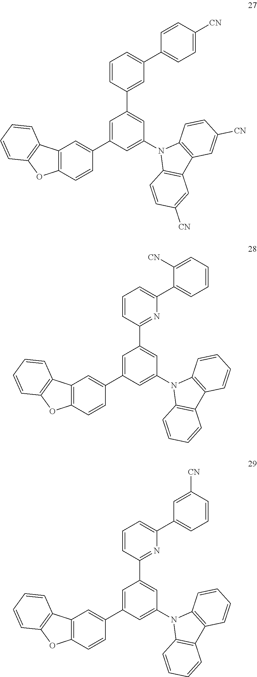

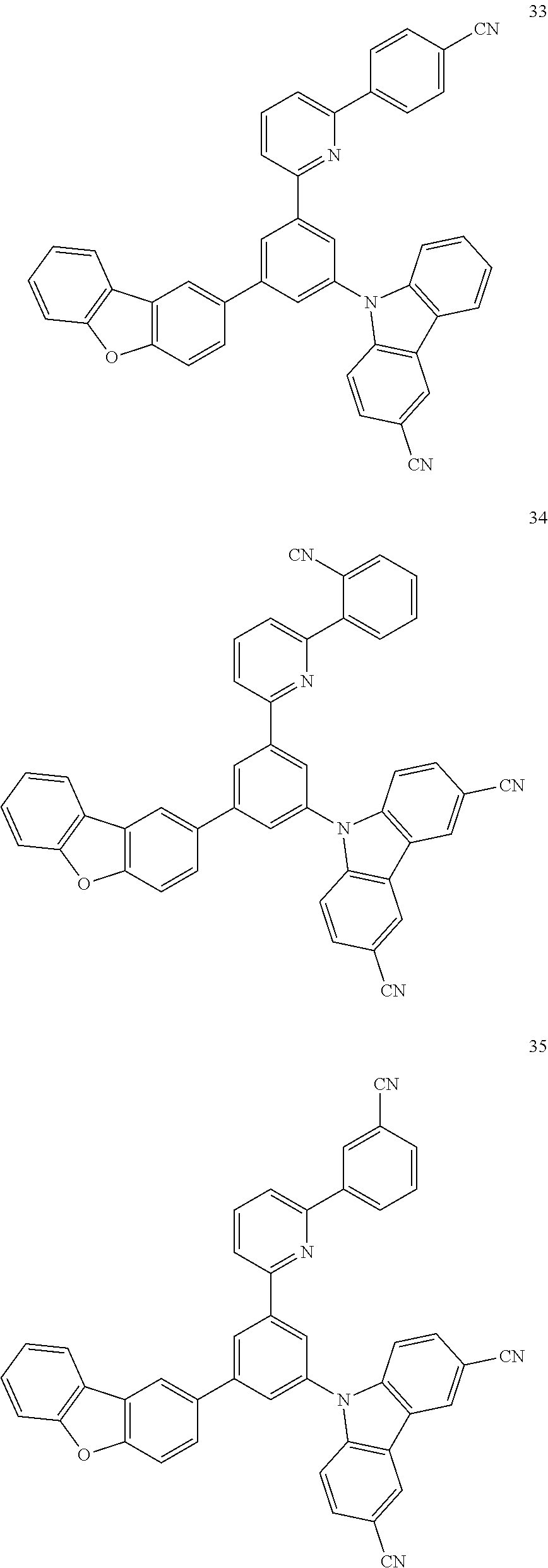


| TABLE 1 | ||||
| Compound No. | HOMO (eV) | LUMO (eV) | T1 (eV) | S1 (eV) |
| 1 | −5.29 | −1.67 | 3 | 3.13 |
| 2 | −5.48 | −1.62 | 3.04 | 3.38 |
| 3 | −5.53 | −1.86 | 2.94 | 3.2 |
| 4 | −5.73 | −1.85 | 3.07 | 3.38 |
| 5 | −5.91 | −1.8 | 3.06 | 3.63 |
| 6 | −5.97 | −2.04 | 2.97 | 3.45 |
| 7 | −6.13 | −2.03 | 3.08 | 3.61 |
| 8 | −6.31 | −1.97 | 3.06 | 3.84 |
| 9 | −6.36 | −2.21 | 2.98 | 3.66 |
| 10 | −5.36 | −1.59 | 3.07 | 3.29 |
| 11 | −5.38 | −1.52 | 3.08 | 3.4 |
| 12 | −5.37 | −1.73 | 3.05 | 3.16 |
| 13 | −5.8 | −1.76 | 3.09 | 3.56 |
| 14 | −5.82 | −1.68 | 3.08 | 3.68 |
| 15 | −5.8 | −1.9 | 3.07 | 3.43 |
| 16 | −6.2 | −1.9 | 3.08 | 3.82 |
| 17 | −6.22 | −1.8 | 3.08 | 3.94 |
| 18 | −6.2 | −2.03 | 3.08 | 3.71 |
| 19 | −5.3 | −1.6 | 3.04 | 3.33 |
| 20 | −5.37 | −1.55 | 3.04 | 3.46 |
| 21 | −5.47 | −1.76 | 2.98 | 3.35 |
| 22 | −5.72 | −1.76 | 3.03 | 3.58 |
| 23 | −5.81 | −1.68 | 3.05 | 3.73 |
| 24 | −5.9 | −1.89 | 2.99 | 3.66 |
| 25 | −6.07 | −1.93 | 2.99 | 3.75 |
| 26 | −6.22 | −1.77 | 3.06 | 3.95 |
| 27 | −6.29 | −1.97 | 2.99 | 3.94 |
| 28 | −5.42 | −1.8 | 2.94 | 3.26 |
| 29 | −5.46 | −1.75 | 2.93 | 3.3 |
| 30 | −5.47 | −2 | 2.85 | 3.13 |
| 31 | −5.85 | −1.93 | 2.96 | 3.55 |
| 32 | −5.9 | −1.87 | 2.95 | 3.55 |
| 33 | −5.9 | −2.12 | 2.86 | 3.44 |
| 34 | −6.24 | −2.04 | 2.97 | 3.78 |
| 35 | −6.28 | −2.02 | 2.95 | 3.74 |
| 36 | −6.28 | −2.24 | 2.86 | 3.67 |
| A | −5.46 | −0.77 | 3.17 | 4.01 |
| B | −5.259 | −0.870 | 3.050 | 3.338 |
| C | −5.357 | −1.099 | 3.114 | 3.372 |
| D | −5.587 | −1.743 | 3.048 | 3.356 |


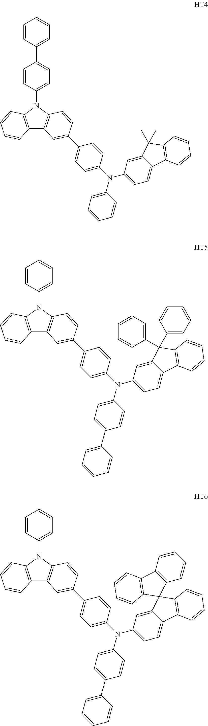


| TABLE 2 | |
| HOMO | A potential (Volts, V) versus current (Amperes, A) graph of each compound |
| energy level | was obtained by using cyclic voltammetry (CV) (electrolyte: 0.1 molar (M) |
| evaluation | Bu4NClO4/solvent: CH2Cl2/electrode: 3-electrode system (working electrode: |
| method | GC, reference electrode: Ag/AgCl, auxiliary electrode: Pt)). Subsequently, |
| from reduction onset of the graph, a HOMO energy level of the compound was | |
| calculated. | |
| LUMO | Each compound was diluted at a concentration of 1 × 10⁻⁵ M in CHCl3, and an |
| energy level | UV absorption spectrum thereof was measured at room temperature by using |
| evaluation | a Shimadzu UV-350 spectrometer. A LUMO energy level thereof was |
| method | calculated by using an optical band gap (Eg) from an edge of the absorption |
| spectrum. | |
| T1 energy | A mixture (each compound was dissolved in an amount of 1 milligram (mg) in 3 |
| level | cubic centimeters (cc) of toluene) of toluene and each compound was loaded |
| evaluation | into a quartz cell. Subsequently, the resultant quartz cell was loaded into liquid |
| method | nitrogen (77 Kelvins (K)), a photoluminescence spectrum thereof was |
| measured by using a device for measuring photoluminescence. The obtained | |
| spectrum was compared with a photoluminescence spectrum measured at | |
| room temperature, and peaks observed only at a low temperature were | |
| analyzed to calculate T1 energy levels. | |

| TABLE 3 | |||||
| Compound No. | HOMO (eV) | LUMO (eV) | T1 (eV) | ||
| |
−5.68 | −2.11 | 3.04 | ||
| Compound 55 | −5.34 | −1.84 | 3.05 | ||
| Compound B | −5.91 | −2.46 | 2.74 | ||
| Compound C | −5.91 | −2.34 | 2.77 | ||
| TABLE 4 | |||
| Compound No. | Tg (° C.) | ||
| |
106 | ||
| Compound 55 | 129 | ||
| |
96 | ||
| Compound C | 64 | ||


| TABLE 5 | ||||||
| Quantum | ||||||
| Driving | Efficiency | efficiency | ||||
| Host | voltage (V) | (Cd/A) | Efficiency/y | (%) | Lifespan (Hours) | |
| Example 1 | Compound | 5.03 | 37.99 | 141.2 | 20.0 | 44.67 |
| 1 | ||||||
| Comparative | Compound | 5.85 | 29.30 | 1 | 16.3 | 0.67 |
| Example 1 | A | |||||
| Comparative | Compound | 5.05 | 32.83 | 130.1 | 18.1 | 21.71 |
| Example 2 | D | |||||
Claims (20)


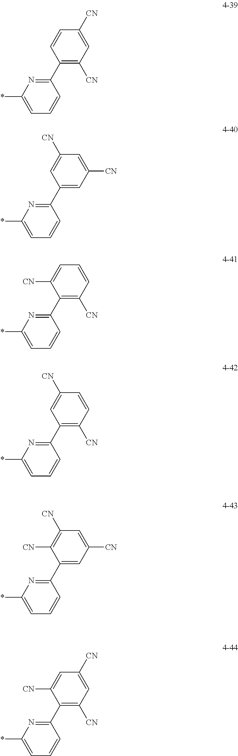


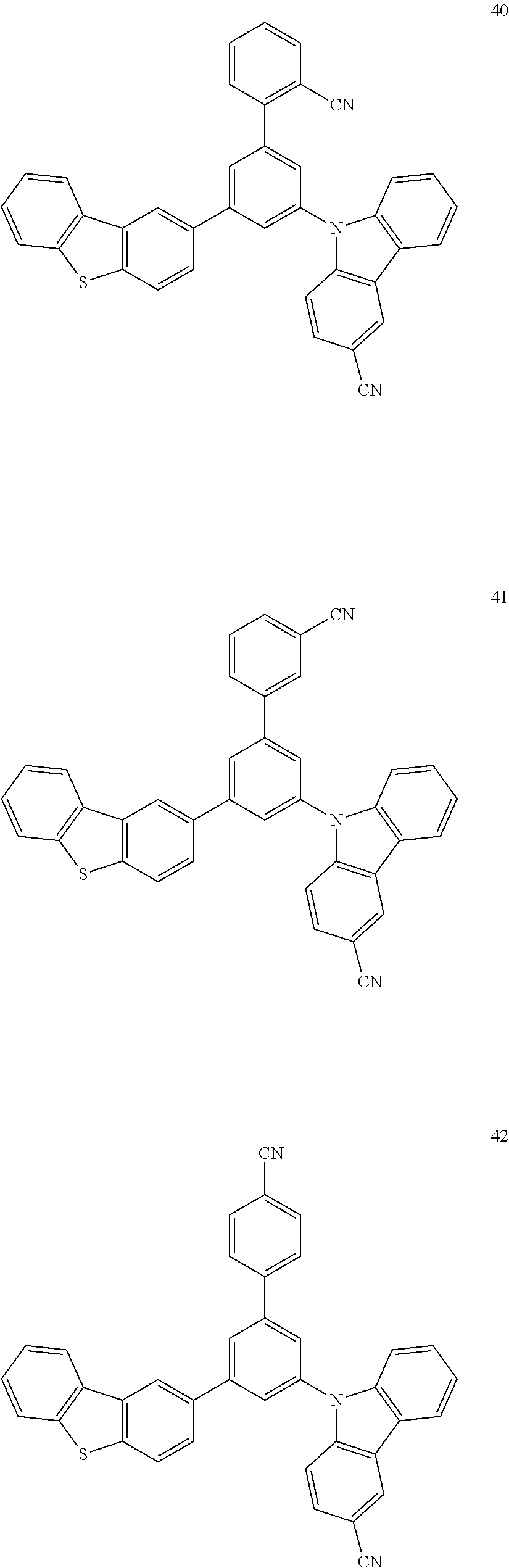


Applications Claiming Priority (2)
| Application Number | Priority Date | Filing Date | Title |
|---|---|---|---|
| KR10-2015-0117335 | 2015-08-20 | ||
| KR1020150117335A KR102463894B1 (en) | 2015-08-20 | 2015-08-20 | Condensed cyclic compound and organic light emitting device including the same |
Publications (2)
| Publication Number | Publication Date |
|---|---|
| US20170054082A1 US20170054082A1 (en) | 2017-02-23 |
| US10193082B2 true US10193082B2 (en) | 2019-01-29 |
Family
ID=58157954
Family Applications (1)
| Application Number | Title | Priority Date | Filing Date |
|---|---|---|---|
| US15/093,412 Active 2036-05-18 US10193082B2 (en) | 2015-08-20 | 2016-04-07 | Condensed-cyclic compound and organic light emitting device including the same |
Country Status (2)
| Country | Link |
|---|---|
| US (1) | US10193082B2 (en) |
| KR (1) | KR102463894B1 (en) |
Families Citing this family (7)
| Publication number | Priority date | Publication date | Assignee | Title |
|---|---|---|---|---|
| WO2018134261A1 (en) * | 2017-01-18 | 2018-07-26 | Basf Se | Fluorescent colorants based on cyanoaryl-substituted naphthoylenebenzimidazole compounds |
| EP3556746A1 (en) * | 2018-04-18 | 2019-10-23 | Novaled GmbH | Compound, method for preparing the same, organic semiconducting layer, organic electronic device, display and lighting device comprising the same |
| KR101981005B1 (en) | 2018-05-11 | 2019-05-21 | 박기철 | The image projection glass exchange device for logo light |
| KR102692561B1 (en) * | 2018-06-26 | 2024-08-06 | 삼성전자주식회사 | Organic light emitting device |
| US12114517B2 (en) | 2019-03-22 | 2024-10-08 | Sharp Kabushiki Kaisha | Light-emitting element and light-emitting device |
| KR102766084B1 (en) * | 2019-07-23 | 2025-02-10 | 엘지디스플레이 주식회사 | Organic compounds, and organic light emitting diode and orgnic light emitting display device including the same |
| US12538636B2 (en) * | 2020-03-26 | 2026-01-27 | Sharp Kabushiki Kaisha | Light-emitting element and display device |
Citations (8)
| Publication number | Priority date | Publication date | Assignee | Title |
|---|---|---|---|---|
| US20090030202A1 (en) | 2007-07-10 | 2009-01-29 | Idemitsu Kosan Co., Ltd. | Material for organic electroluminescent element and organic electroluminescent element employing the same |
| JP2012033892A (en) | 2010-06-30 | 2012-02-16 | Fujifilm Corp | Material for light-emitting element and light-emitting element |
| JP2013075891A (en) | 2011-09-15 | 2013-04-25 | Idemitsu Kosan Co Ltd | Aromatic amine derivative and organic electroluminescence element using the same |
| KR20130127994A (en) | 2010-12-13 | 2013-11-25 | 메르크 파텐트 게엠베하 | Substituted tetraarylbenzenes |
| KR20140046541A (en) * | 2012-10-04 | 2014-04-21 | 롬엔드하스전자재료코리아유한회사 | Novel organic electroluminescence compounds and organic electroluminescence device comprising the same |
| KR20140132244A (en) * | 2013-05-07 | 2014-11-17 | 주식회사 엘지화학 | Hetero-cyclic compound and organic electronic device comprising the same |
| KR20140138393A (en) | 2013-05-23 | 2014-12-04 | 주식회사 파마코스텍 | Asymmetric ortho-Terphenyl Derivatives and Organic light emitting device Comprising the Same |
| US9318709B2 (en) * | 2012-05-24 | 2016-04-19 | Idemitsu Kosan Co., Ltd. | Material for organic electroluminescence device, and organic electroluminescence device using the same |
Family Cites Families (1)
| Publication number | Priority date | Publication date | Assignee | Title |
|---|---|---|---|---|
| KR101764464B1 (en) * | 2014-01-27 | 2017-08-04 | 단국대학교 산학협력단 | Bipolar organic material and oled having the same |
-
2015
- 2015-08-20 KR KR1020150117335A patent/KR102463894B1/en active Active
-
2016
- 2016-04-07 US US15/093,412 patent/US10193082B2/en active Active
Patent Citations (10)
| Publication number | Priority date | Publication date | Assignee | Title |
|---|---|---|---|---|
| US20090030202A1 (en) | 2007-07-10 | 2009-01-29 | Idemitsu Kosan Co., Ltd. | Material for organic electroluminescent element and organic electroluminescent element employing the same |
| JP2012033892A (en) | 2010-06-30 | 2012-02-16 | Fujifilm Corp | Material for light-emitting element and light-emitting element |
| KR20130127994A (en) | 2010-12-13 | 2013-11-25 | 메르크 파텐트 게엠베하 | Substituted tetraarylbenzenes |
| US20150057445A1 (en) | 2010-12-13 | 2015-02-26 | Merck Patent Gmbh | Substituted tetraarylbenzenes |
| JP2013075891A (en) | 2011-09-15 | 2013-04-25 | Idemitsu Kosan Co Ltd | Aromatic amine derivative and organic electroluminescence element using the same |
| US20140374720A1 (en) | 2011-09-15 | 2014-12-25 | Idemitsu Kosan Co., Ltd. | Aromatic amine derivative and organic electroluminescence element using same |
| US9318709B2 (en) * | 2012-05-24 | 2016-04-19 | Idemitsu Kosan Co., Ltd. | Material for organic electroluminescence device, and organic electroluminescence device using the same |
| KR20140046541A (en) * | 2012-10-04 | 2014-04-21 | 롬엔드하스전자재료코리아유한회사 | Novel organic electroluminescence compounds and organic electroluminescence device comprising the same |
| KR20140132244A (en) * | 2013-05-07 | 2014-11-17 | 주식회사 엘지화학 | Hetero-cyclic compound and organic electronic device comprising the same |
| KR20140138393A (en) | 2013-05-23 | 2014-12-04 | 주식회사 파마코스텍 | Asymmetric ortho-Terphenyl Derivatives and Organic light emitting device Comprising the Same |
Non-Patent Citations (1)
| Title |
|---|
| Deng et al., Simple bipolar host materials incorporating CN group for highly efficient blue electrophosphorescence with slow efficiency roll-off, Journal of Materials Chemistry C: Materials for Optical and Electronic Devices (2013), 1(48), 8140-8145. * |
Also Published As
| Publication number | Publication date |
|---|---|
| US20170054082A1 (en) | 2017-02-23 |
| KR102463894B1 (en) | 2022-11-07 |
| KR20170022411A (en) | 2017-03-02 |
Similar Documents
| Publication | Publication Date | Title |
|---|---|---|
| US11785840B2 (en) | Organometallic compound, organic light-emitting device including the organometallic compound, and diagnosis composition including the organometallic compound | |
| US12089487B2 (en) | Organometallic compound and organic light-emitting device including the same | |
| US12358876B2 (en) | Condensed cyclic compound and organic light-emitting device including the same | |
| US10593891B2 (en) | Condensed cyclic compound and organic light-emitting device including the same | |
| US9960367B2 (en) | Condensed cyclic compound and organic light-emitting device including the same | |
| US10062852B2 (en) | Condensed cyclic compound and organic light-emitting device including the same | |
| US10505124B2 (en) | Carbazole-based compound and organic light-emitting device including the same | |
| US10193080B2 (en) | Condensed cyclic compound and organic light-emitting device including the same | |
| US20210050533A1 (en) | Organometallic compound and organic light-emitting device including the same | |
| US20180062088A1 (en) | Organometallic compound, organic light-emitting device including the organometallic compound, and diagnostic composition including the organometallic compound | |
| US10043983B2 (en) | Condensed cyclic compound and organic light-emitting device including the same | |
| US20160013423A1 (en) | Condensed cyclic compound and organic light-emitting device including the same | |
| US10629829B2 (en) | Organometallic compound and organic light-emitting device including the same | |
| US20160028030A1 (en) | Condensed cyclic compound and organic light-emitting device including the same | |
| US10193082B2 (en) | Condensed-cyclic compound and organic light emitting device including the same | |
| US20160035986A1 (en) | Condensed cyclic compound and organic light-emitting device including the same | |
| US20170069853A1 (en) | Condensed cyclic comopund and organic light-emitting device including the same | |
| US20170358756A1 (en) | Condensed cyclic compound and organic light-emitting device including the same | |
| US10714696B2 (en) | Organometallic compound and organic light-emitting device including the same | |
| US10367151B2 (en) | Condensed cyclic compound and organic light-emitting device including the same | |
| US10043984B2 (en) | Condensed cyclic compound and organic light-emitting device including the same | |
| US20220271237A1 (en) | Condensed cyclic comopund and organic light-emitting device including the same | |
| US9960365B2 (en) | Condensed cyclic compound and organic light-emitting device including the same | |
| US11469381B2 (en) | Condensed cyclic compound and organic light-emitting device including the same | |
| US20190334095A1 (en) | Condensed cyclic compound and organic light-emitting device including the same |
Legal Events
| Date | Code | Title | Description |
|---|---|---|---|
| AS | Assignment |
Owner name: SAMSUNG ELECTRONICS CO., LTD., KOREA, REPUBLIC OF Free format text: ASSIGNMENT OF ASSIGNORS INTEREST;ASSIGNORS:KIM, HYUNJUNG;CHAE, MIYOUNG;KIM, SANGMO;AND OTHERS;REEL/FRAME:038292/0222 Effective date: 20160404 Owner name: SAMSUNG SDI CO., LTD., KOREA, REPUBLIC OF Free format text: ASSIGNMENT OF ASSIGNORS INTEREST;ASSIGNORS:KIM, HYUNJUNG;CHAE, MIYOUNG;KIM, SANGMO;AND OTHERS;REEL/FRAME:038292/0222 Effective date: 20160404 |
|
| STCF | Information on status: patent grant |
Free format text: PATENTED CASE |
|
| AS | Assignment |
Owner name: SAMSUNG ELECTRONICS CO., LTD., KOREA, REPUBLIC OF Free format text: ASSIGNMENT OF ASSIGNORS INTEREST;ASSIGNORS:SAMSUNG ELECTRONICS CO., LTD.;SAMSUNG SDI CO., LTD.;REEL/FRAME:051366/0480 Effective date: 20191205 Owner name: SAMSUNG SDI CO., LTD., KOREA, REPUBLIC OF Free format text: ASSIGNMENT OF ASSIGNORS INTEREST;ASSIGNORS:SAMSUNG ELECTRONICS CO., LTD.;SAMSUNG SDI CO., LTD.;REEL/FRAME:051366/0480 Effective date: 20191205 |
|
| MAFP | Maintenance fee payment |
Free format text: PAYMENT OF MAINTENANCE FEE, 4TH YEAR, LARGE ENTITY (ORIGINAL EVENT CODE: M1551); ENTITY STATUS OF PATENT OWNER: LARGE ENTITY Year of fee payment: 4 |