US10186620B1 - InGaAlP schottky field effect transistor with stepped bandgap ohmic contact - Google Patents
InGaAlP schottky field effect transistor with stepped bandgap ohmic contact Download PDFInfo
- Publication number
- US10186620B1 US10186620B1 US15/797,479 US201715797479A US10186620B1 US 10186620 B1 US10186620 B1 US 10186620B1 US 201715797479 A US201715797479 A US 201715797479A US 10186620 B1 US10186620 B1 US 10186620B1
- Authority
- US
- United States
- Prior art keywords
- layer
- bandgap
- schottky
- ingaalp
- effect transistor
- Prior art date
- Legal status (The legal status is an assumption and is not a legal conclusion. Google has not performed a legal analysis and makes no representation as to the accuracy of the status listed.)
- Active
Links
- 230000005669 field effect Effects 0.000 title claims abstract description 54
- 230000004888 barrier function Effects 0.000 claims abstract description 61
- 229910052751 metal Inorganic materials 0.000 claims abstract description 15
- 239000002184 metal Substances 0.000 claims abstract description 15
- 150000001875 compounds Chemical class 0.000 claims abstract description 11
- 239000004065 semiconductor Substances 0.000 claims abstract description 11
- 239000000758 substrate Substances 0.000 claims abstract description 11
- 238000005530 etching Methods 0.000 claims description 22
- 229910001218 Gallium arsenide Inorganic materials 0.000 claims description 20
- 239000000463 material Substances 0.000 claims description 14
- 229910052782 aluminium Inorganic materials 0.000 claims description 10
- XAGFODPZIPBFFR-UHFFFAOYSA-N aluminium Chemical compound [Al] XAGFODPZIPBFFR-UHFFFAOYSA-N 0.000 claims description 10
- 125000006850 spacer group Chemical group 0.000 description 32
- 229910000980 Aluminium gallium arsenide Inorganic materials 0.000 description 14
- GYHNNYVSQQEPJS-UHFFFAOYSA-N Gallium Chemical compound [Ga] GYHNNYVSQQEPJS-UHFFFAOYSA-N 0.000 description 9
- 229910052733 gallium Inorganic materials 0.000 description 9
- 238000010586 diagram Methods 0.000 description 6
- 230000003321 amplification Effects 0.000 description 4
- 238000003199 nucleic acid amplification method Methods 0.000 description 4
- 230000003247 decreasing effect Effects 0.000 description 2
- 230000004048 modification Effects 0.000 description 2
- 238000012986 modification Methods 0.000 description 2
- 238000000059 patterning Methods 0.000 description 2
- 229910000530 Gallium indium arsenide Inorganic materials 0.000 description 1
- 230000015556 catabolic process Effects 0.000 description 1
- 230000000694 effects Effects 0.000 description 1
- 230000003631 expected effect Effects 0.000 description 1
- 229910052738 indium Inorganic materials 0.000 description 1
- APFVFJFRJDLVQX-UHFFFAOYSA-N indium atom Chemical group [In] APFVFJFRJDLVQX-UHFFFAOYSA-N 0.000 description 1
- 230000000630 rising effect Effects 0.000 description 1
Images


Classifications
-
- H—ELECTRICITY
- H10—SEMICONDUCTOR DEVICES; ELECTRIC SOLID-STATE DEVICES NOT OTHERWISE PROVIDED FOR
- H10D—INORGANIC ELECTRIC SEMICONDUCTOR DEVICES
- H10D30/00—Field-effect transistors [FET]
- H10D30/80—FETs having rectifying junction gate electrodes
- H10D30/87—FETs having Schottky gate electrodes, e.g. metal-semiconductor FETs [MESFET]
-
- H01L29/812—
-
- H01L29/205—
-
- H01L29/42312—
-
- H—ELECTRICITY
- H10—SEMICONDUCTOR DEVICES; ELECTRIC SOLID-STATE DEVICES NOT OTHERWISE PROVIDED FOR
- H10D—INORGANIC ELECTRIC SEMICONDUCTOR DEVICES
- H10D30/00—Field-effect transistors [FET]
- H10D30/40—FETs having zero-dimensional [0D], one-dimensional [1D] or two-dimensional [2D] charge carrier gas channels
- H10D30/47—FETs having zero-dimensional [0D], one-dimensional [1D] or two-dimensional [2D] charge carrier gas channels having 2D charge carrier gas channels, e.g. nanoribbon FETs or high electron mobility transistors [HEMT]
- H10D30/471—High electron mobility transistors [HEMT] or high hole mobility transistors [HHMT]
- H10D30/475—High electron mobility transistors [HEMT] or high hole mobility transistors [HHMT] having wider bandgap layer formed on top of lower bandgap active layer, e.g. undoped barrier HEMTs such as i-AlGaN/GaN HEMTs
- H10D30/4755—High electron mobility transistors [HEMT] or high hole mobility transistors [HHMT] having wider bandgap layer formed on top of lower bandgap active layer, e.g. undoped barrier HEMTs such as i-AlGaN/GaN HEMTs having wide bandgap charge-carrier supplying layers, e.g. modulation doped HEMTs such as n-AlGaAs/GaAs HEMTs
-
- H—ELECTRICITY
- H10—SEMICONDUCTOR DEVICES; ELECTRIC SOLID-STATE DEVICES NOT OTHERWISE PROVIDED FOR
- H10D—INORGANIC ELECTRIC SEMICONDUCTOR DEVICES
- H10D62/00—Semiconductor bodies, or regions thereof, of devices having potential barriers
- H10D62/10—Shapes, relative sizes or dispositions of the regions of the semiconductor bodies; Shapes of the semiconductor bodies
- H10D62/13—Semiconductor regions connected to electrodes carrying current to be rectified, amplified or switched, e.g. source or drain regions
- H10D62/149—Source or drain regions of field-effect devices
- H10D62/161—Source or drain regions of field-effect devices of FETs having Schottky gates
-
- H—ELECTRICITY
- H10—SEMICONDUCTOR DEVICES; ELECTRIC SOLID-STATE DEVICES NOT OTHERWISE PROVIDED FOR
- H10D—INORGANIC ELECTRIC SEMICONDUCTOR DEVICES
- H10D62/00—Semiconductor bodies, or regions thereof, of devices having potential barriers
- H10D62/80—Semiconductor bodies, or regions thereof, of devices having potential barriers characterised by the materials
- H10D62/82—Heterojunctions
- H10D62/824—Heterojunctions comprising only Group III-V materials heterojunctions, e.g. GaN/AlGaN heterojunctions
-
- H—ELECTRICITY
- H10—SEMICONDUCTOR DEVICES; ELECTRIC SOLID-STATE DEVICES NOT OTHERWISE PROVIDED FOR
- H10D—INORGANIC ELECTRIC SEMICONDUCTOR DEVICES
- H10D64/00—Electrodes of devices having potential barriers
- H10D64/20—Electrodes characterised by their shapes, relative sizes or dispositions
- H10D64/27—Electrodes not carrying the current to be rectified, amplified, oscillated or switched, e.g. gates
- H10D64/311—Gate electrodes for field-effect devices
Definitions
- the present invention relates to an InGaAlP Schottky field effect transistor, especially related to an InGaAlP Schottky field effect transistor with stepped bandgap ohmic contact.
- FIG. 10 is a sectional schematic view of an embodiment of an InGaAlP Schottky field effect transistor of conventional technology.
- the main structure of the InGaAlP Schottky field effect transistor 9 of conventional technology comprises: a compound semiconductor substrate 901 , a buffer layer 902 , a lower barrier layer 920 , a first spacer layer 906 , a channel layer 907 , a second spacer layer 908 , an upper barrier layer 930 , a cap layer 912 , a source electrode 916 ( 913 ), a drain electrode 917 ( 913 ), a gate recess 915 and a gate electrode 914 .
- the compound semiconductor substrate 901 is made of GaAs.
- the buffer layer 902 is formed on the compound semiconductor substrate 901 , wherein the buffer layer 902 is made of GaAs.
- the lower barrier layer 920 is formed on the buffer layer 902 , wherein the lower barrier layer 920 is made of AlGaAs.
- the lower barrier layer 920 comprises a lower-barrier sub-layer 903 , a lower carrier supply layer 904 and a lower-barrier spacer layer 905 , wherein the lower-barrier sub-layer 903 is formed on the buffer layer 902 ; the lower carrier supply layer 904 is formed on the lower-barrier sub-layer 903 ; the lower-barrier spacer layer 905 is formed on the lower carrier supply layer 904 .
- the first spacer layer 906 is formed on the lower-barrier spacer layer 905 of the lower barrier layer 920 , wherein the first spacer layer 906 is made of GaAs.
- the channel layer 907 is formed on the first spacer layer 906 , wherein the channel layer 907 is made of InGaAs.
- the second spacer layer 908 is formed on the channel layer 907 , wherein the second spacer layer 908 is made of GaAs.
- the upper barrier layer 930 is formed on the second spacer layer 908 , wherein the upper barrier layer 930 is made of InGaAlP.
- the upper barrier layer 930 comprises an upper-barrier spacer layer 909 , an upper carrier supply layer 910 and a Schottky barrier layer 911 , wherein the upper-barrier spacer layer 909 is formed on the second spacer layer 908 ; the upper carrier supply layer 910 is formed on the upper-barrier spacer layer 909 ; the Schottky barrier layer 911 is formed on the upper carrier supply layer 910 .
- the cap layer 912 is formed on the Schottky barrier layer 911 of the upper barrier layer 930 , wherein the cap layer 912 is made of GaAs.
- An ohmic electrode layer 913 is formed on the cap layer 912 , wherein the ohmic electrode layer 913 and the cap layer 912 form an ohmic contact.
- the ohmic electrode layer 913 and the cap layer 912 form the ohmic contact to form the source electrode 916 ; while, in the right side of FIG. 10 , the ohmic electrode layer 913 and the cap layer 912 form the ohmic contact to form the drain electrode 917 .
- the gate electrode 914 is formed on the Schottky barrier layer 911 within the gate recess 915 . And the gate electrode 914 and the Schottky barrier layer 911 form a Schottky contact.
- the material of the Schottky barrier layer 911 is based on InGaAlP instead of the more commonly used AlGaAs in conventional technology.
- the bandgap of InGaAlP is higher than the bandgap of AlGaAs, when comparing the field effect transistor 9 having the InGaAlP (higher bandgap) Schottky barrier layer 911 and the field effect transistor having the AlGaAs (lower bandgap) Schottky barrier layer, the field effect transistor 9 having the InGaAlP (higher bandgap) Schottky barrier layer 911 has a lower leakage current and a higher breakdown voltage.
- the material of the Schottky barrier layer 911 is InGaAlP which has a higher bandgap such that the bankgap difference between the Schottky barrier layer 911 and the cap layer 912 will be too huge. Hence, it will result in a barrier to the electron current and will affects the performance of the field effect transistor 9 , such as increasing the on-state resistance (Ron), reducing the high speed switching ability and decreasing the microwave amplification gain.
- the present invention has developed a new design which may avoid the above mentioned drawbacks, may significantly enhance the performance of the devices and may take into account economic considerations. Therefore, the present invention then has been invented.
- the main technical problem that the present invention is seeking to solve is to narrow the bankgap difference between the InGaAlP Schottky barrier layer and the cap layer so that the on-state resistance (Ron) of the InGaAlP Schottky field effect transistor will be decreased, the high speed switching ability of the InGaAlP Schottky field effect transistor will be enhanced, and the microwave amplification gain will be increased.
- the present invention provides an InGaAlP Schottky field effect transistor with stepped bandgap ohmic contact comprising: a compound semiconductor substrate, a buffer layer, a channel layer, a carrier supply layer, a Schottky barrier layer, an intermediate bandgap layer, a cap layer and an ohmic metal layer, wherein the buffer layer is formed on the compound semiconductor substrate; the channel layer is formed on the buffer layer; the carrier supply layer is formed on the channel layer; the Schottky barrier layer is formed on the carrier supply layer, wherein the Schottky barrier layer is made of InGaAlP; the intermediate bandgap layer is formed on the Schottky barrier layer; the cap layer is formed on the intermediate bandgap layer; the ohmic metal layer is formed on the cap layer, wherein the ohmic metal layer and the cap layer form an ohmic contact; wherein the Schottky barrier layer, the intermediate bandgap layer and the
- the intermediate bandgap layer is made of Al x Ga 1-x As.
- the aluminum composition x is greater than or equal to 0.1 and less than or equal to 0.3.
- the intermediate bandgap layer is made of at least one material selected from the group consisting of: InGaP, InGaAsP and InAlP.
- the InGaAlP Schottky field effect transistor with stepped bandgap ohmic contact it further comprises an etching stop layer, wherein the etching stop layer is formed between the intermediate bandgap layer and the cap layer.
- the etching stop layer is made of AlAs.
- the cap layer is made of GaAs.
- FIG. 1 is a sectional schematic view of an embodiment of an InGaAlP Schottky field effect transistor with stepped bandgap ohmic contact of the present invention.
- FIG. 2 is a sectional schematic view of an embodiment of another InGaAlP Schottky field effect transistor with stepped bandgap ohmic contact of the present invention.
- FIG. 3 is a sectional schematic view of an embodiment of an InGaAlP Schottky field effect transistor with stepped bandgap ohmic contact of the present invention.
- FIG. 4 is a sectional schematic view of an embodiment of another InGaAlP Schottky field effect transistor with stepped bandgap ohmic contact of the present invention.
- FIG. 5 is a sectional schematic view of an embodiment of an InGaAlP Schottky field effect transistor with stepped bandgap ohmic contact of the present invention.
- FIG. 6 is a sectional schematic view of an embodiment of another InGaAlP Schottky field effect transistor with stepped bandgap ohmic contact of the present invention.
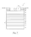
- FIG. 7 is a sectional schematic view of an embodiment of an InGaAlP Schottky field effect transistor with stepped bandgap ohmic contact of the present invention.
- FIG. 8 is a sectional schematic view of an embodiment of another InGaAlP Schottky field effect transistor with stepped bandgap ohmic contact of the present invention.
- FIG. 9A is a schematic diagram of the bandgap of an embodiment of an InGaAlP Schottky field effect transistor with stepped bandgap ohmic contact of the present invention.
- FIG. 9B is a schematic diagram of the bandgap of another embodiment of an InGaAlP Schottky field effect transistor with stepped bandgap ohmic contact of the present invention.
- FIG. 10 is a sectional schematic view of an embodiment of an InGaAlP Schottky field effect transistor of conventional technology.
- FIG. 1 is a sectional schematic view of an embodiment of an InGaAlP Schottky field effect transistor with stepped bandgap ohmic contact of the present invention.
- An InGaAlP Schottky field effect transistor 1 with stepped bandgap ohmic contact of the present invention comprises: a compound semiconductor substrate 10 , a buffer layer 12 , a channel layer 32 , a carrier supply layer 44 , a Schottky barrier layer 50 , an intermediate bandgap layer 60 , a cap layer 70 , an ohmic metal layer 80 , a gate recess 95 and a gate electrode 90 .
- the compound semiconductor substrate 10 is made of GaAs.
- the buffer layer 12 is formed on the compound semiconductor substrate 10 , wherein the buffer layer 12 is made of GaAs or AlGaAs.
- the channel layer 32 is formed on the buffer layer 12 , wherein the channel layer 32 is made of In x Ga 1-x As, wherein the ratio of the composition of indium to gallium is x:1 ⁇ x, wherein x is greater than or equal to 0.2 and less than or equal to 0.5. In a preferable embodiment, x is greater than or equal to 0.3 and less than or equal to 0.4.
- the carrier supply layer 44 is formed on the channel layer 32 , wherein the carrier supply layer 44 is made of at least one material selected from the group consisting of: GaAs, AlGaAs, InGaP and InGaAlP.
- the Schottky barrier layer 50 is formed on the carrier supply layer 44 , wherein the Schottky barrier layer 50 is made of InGaAlP.
- the intermediate bandgap layer 60 is formed on the Schottky barrier layer 50 , wherein the intermediate bandgap layer 60 is made of at least one material selected from the group consisting of: InGaP, InGaAsP, InAlP and AlGaAs.
- the intermediate bandgap layer 60 is made of Al x Ga 1-x As, wherein the ratio of the composition of aluminum to gallium is x:1 ⁇ x, wherein x is greater than or equal to 0.1 and less than or equal to 0.3.
- the cap layer 70 is formed on the intermediate bandgap layer 60 , wherein the cap layer 70 is made of GaAs.
- the ohmic metal layer 80 is formed on the cap layer 70 , wherein the ohmic metal layer 80 and the cap layer 70 form an ohmic contact.
- the cap layer 70 is formed of the material of GaAs doped with Si with a high concentration. Patterning the ohmic metal layer 80 and then etching the cap layer 70 and the intermediate bandgap layer 60 to form the gate recess 95 , wherein the etching is stopped at the Schottky barrier layer 50 such that a bottom of the gate recess 95 is defined by the Schottky barrier layer 50 .
- the gate electrode 90 is formed on the Schottky barrier layer 50 within the gate recess 95 . And the gate electrode 90 and the Schottky barrier layer 50 form a Schottky contact.
- the ohmic metal layer 80 and the cap layer 70 form the ohmic contact to form a source electrode 801 ; while, in the right side of FIG. 1 , the ohmic metal layer 80 and the cap layer 70 form the ohmic contact to form the drain electrode 802 .
- the Schottky barrier layer 50 , the intermediate bandgap layer 60 and the cap layer 70 have a Schottky-barrier-layer bandgap, an intermediate bandgap and a cap-layer bandgap respectively, wherein the intermediate bandgap is less than the Schottky-barrier-layer bandgap and greater than the cap-layer bandgap.
- FIG. 9A is a schematic diagram of the bandgap of an embodiment of an InGaAlP Schottky field effect transistor with stepped bandgap ohmic contact of the present invention.
- FIG. 9A is a schematic diagram of the bandgap of an embodiment of an InGaAlP Schottky field effect transistor with stepped bandgap ohmic contact of the present invention.
- FIG. 9A shows the schematic diagram of the bandgap of the channel layer 32 , the carrier supply layer 44 , the Schottky barrier layer 50 , the intermediate bandgap layer 60 , the cap layer 70 and the ohmic metal layer 80 (including the source electrode 801 and the drain electrode 802 ) of the embodiment of FIG. 1 . If there is no such an intermediate bandgap layer 60 , then the bankgap difference between the Schottky barrier layer 50 and the cap layer 70 will be too huge.
- the present invention provides the intermediate bandgap layer 60 formed between the Schottky barrier layer 50 and the cap layer 70 .
- the intermediate bandgap of the intermediate bandgap layer 60 is less than the Schottky-barrier-layer bandgap of the Schottky barrier layer 50 and greater than the cap-layer bandgap of the cap layer 70 , therefore, the present invention provides the stepped bandgap layer (the intermediate bandgap layer 60 ) to lower down the bankgap difference between the Schottky barrier layer 50 and the cap layer 70 such that the on-state resistance (Ron) of the InGaAlP Schottky field effect transistor 1 with stepped bandgap ohmic contact of the present invention is reduced.
- Ron on-state resistance
- the intermediate bandgap layer 60 is made of Al x Ga 1-x As, wherein the ratio of the composition of aluminum to gallium is x:1 ⁇ x, wherein x is greater than or equal to 0.1 and less than or equal to 0.28, greater than or equal to 0.1 and less than or equal to 0.26, greater than or equal to 0.1 and less than or equal to 0.24, greater than or equal to 0.1 and less than or equal to 0.22, greater than or equal to 0.1 and less than or equal to 0.2, greater than or equal to 0.12 and less than or equal to 0.3, greater than or equal to 0.14 and less than or equal to 0.3, greater than or equal to 0.16 and less than or equal to 0.3, greater than or equal to 0.18 and less than or equal to 0.3 or greater than or equal to 0.2 and less than or equal to 0.3.
- FIG. 2 is a sectional schematic view of an embodiment of another InGaAlP Schottky field effect transistor with stepped bandgap ohmic contact of the present invention.
- the main structure of the embodiment of FIG. 2 is basically the same as the structure of the embodiment of FIG. 1 , except that it further comprises an etching stop layer 61 , wherein the etching stop layer 61 is formed between the intermediate bandgap layer 60 and the cap layer 70 , wherein the etching stop layer 61 is made of AlAs.
- FIG. 3 is a sectional schematic view of an embodiment of an InGaAlP Schottky field effect transistor with stepped bandgap ohmic contact of the present invention.
- the main structure of the embodiment of FIG. 3 is basically the same as the structure of the embodiment of FIG. 1 , except that it further comprises a sub-intermediate bandgap layer 65 , wherein the sub-intermediate bandgap layer 65 is formed between the intermediate bandgap layer 60 and the cap layer 70 .
- the sub-intermediate bandgap layer 65 has a sub-intermediate bandgap, wherein the sub-intermediate bandgap is less than the intermediate bandgap and greater than the cap-layer bandgap.
- the sub-intermediate bandgap layer 65 is made of at least one material selected from the group consisting of: InGaP, InGaAsP, InAlP and AlGaAs.
- the intermediate bandgap layer 60 is made of Al x Ga 1-x As, wherein the ratio of the composition of aluminum to gallium is x:1 ⁇ x, wherein x is greater than or equal to 0.1 and less than or equal to 0.3; while the sub-intermediate bandgap layer 65 is made of Al y Ga 1-y As, wherein the ratio of the composition of aluminum to gallium is y:1 ⁇ y, wherein y is less than x. Please also refer to FIG.
- FIG. 9B which is a schematic diagram of the bandgap of another embodiment of an InGaAlP Schottky field effect transistor with stepped bandgap ohmic contact of the present invention.
- FIG. 9B shows the schematic diagram of the bandgap of the channel layer 32 , the carrier supply layer 44 , the Schottky barrier layer 50 , the intermediate bandgap layer 60 , the sub-intermediate bandgap layer 65 , the cap layer 70 and the ohmic metal layer 80 (including the source electrode 801 and the drain electrode 802 ) of the embodiment of FIG. 3 .
- the present invention provides the intermediate bandgap layer 60 and the sub-intermediate bandgap layer 65 formed between the Schottky barrier layer 50 and the cap layer 70 .
- the intermediate bandgap of the intermediate bandgap layer 60 is less than the Schottky-barrier-layer bandgap of the Schottky barrier layer 50 and greater than the sub-intermediate bandgap of the sub-intermediate bandgap layer 65 ; while the sub-intermediate bandgap of the sub-intermediate bandgap layer 65 is less than the intermediate bandgap of the intermediate bandgap layer 60 and greater than the cap-layer bandgap of the cap layer 70 .
- the present invention provides more slowly rising stepped bandgap layers (the intermediate bandgap layer 60 and the sub-intermediate bandgap layer 65 ) to lower down the bankgap difference between the Schottky barrier layer 50 and the cap layer 70 such that the on-state resistance (Ron) of the InGaAlP Schottky field effect transistor 1 with stepped bandgap ohmic contact of the present invention is reduced.
- Ron on-state resistance
- the high speed switching ability and the microwave amplification gain of the InGaAlP Schottky field effect transistor 1 with stepped bandgap ohmic contact of the present invention are enhanced.
- the intermediate bandgap layer 60 is made of Al x Ga 1-x As, wherein the ratio of the composition of aluminum to gallium is x:1 ⁇ x, wherein x is greater than or equal to 0.1 and less than or equal to 0.28, greater than or equal to 0.1 and less than or equal to 0.26, greater than or equal to 0.1 and less than or equal to 0.24, greater than or equal to 0.1 and less than or equal to 0.22, greater than or equal to 0.1 and less than or equal to 0.2, greater than or equal to 0.12 and less than or equal to 0.3, greater than or equal to 0.14 and less than or equal to 0.3, greater than or equal to 0.16 and less than or equal to 0.3, greater than or equal to 0.18 and less than or equal to 0.3 or greater than or equal to 0.2 and less than or equal to 0.3; while the sub-intermediate bandgap layer 65 is made of Al y Ga 1-y As, wherein the ratio of the composition of aluminum to gallium is y:1 ⁇ y, wherein
- FIG. 4 is a sectional schematic view of an embodiment of another InGaAlP Schottky field effect transistor with stepped bandgap ohmic contact of the present invention.
- the main structure of the embodiment of FIG. 4 is basically the same as the structure of the embodiment of FIG. 3 , except that it further comprises an etching stop layer 66 , wherein the etching stop layer 66 is formed between the sub-intermediate bandgap layer 65 and the cap layer 70 , wherein the etching stop layer 66 is made of AlAs.
- FIG. 5 is a sectional schematic view of an embodiment of an InGaAlP Schottky field effect transistor with stepped bandgap ohmic contact of the present invention.
- the main structure of the embodiment of FIG. 5 is basically the same as the structure of the embodiment of FIG. 1 , except that it further comprises a lower barrier layer 20 , a first spacer layer 30 , a second spacer layer 34 and an upper-barrier spacer layer 42 .
- the lower barrier layer 20 is Ruined on the buffer layer 12 , wherein the lower barrier layer 20 is made of at least one material selected from the group consisting of: GaAs and AlGaAs.
- the first spacer layer 30 is formed on the lower barrier layer 20 , wherein the first spacer layer 30 is made of GaAs.
- the channel layer 32 is formed on the first spacer layer 30 .
- the second spacer layer 34 is formed on the channel layer 32 , wherein the second spacer layer 34 is made of GaAs.
- the upper-barrier spacer layer 42 is formed on the second spacer layer 34 , wherein the upper-barrier spacer layer 42 is made of at least one material selected from the group consisting of: GaAs, AlGaAs, InGaP and InGaAlP.
- the carrier supply layer 44 is formed on the upper-barrier spacer layer 42 .
- the Schottky barrier layer 50 is formed on the carrier supply layer 44 .
- the lower barrier layer 20 comprises a lower-barrier sub-layer 22 , a lower carrier supply layer 24 and a lower-barrier spacer layer 26 .
- the lower-barrier sub-layer 22 is formed on the buffer layer 12 , wherein the lower-barrier sub-layer 22 is made of at least one material selected from the group consisting of: GaAs and AlGaAs.
- the lower carrier supply layer 24 is formed on the lower-barrier sub-layer 22 , wherein the lower carrier supply layer 24 is made of at least one material selected from the group consisting of: GaAs and AlGaAs.
- the lower-barrier spacer layer 26 is formed on the lower carrier supply layer 24 , wherein the lower-barrier spacer layer 26 is made of at least one material selected from the group consisting of: GaAs and AlGaAs.
- the first spacer layer 30 is formed on the lower-barrier spacer layer 26 .
- FIG. 6 is a sectional schematic view of an embodiment of another InGaAlP Schottky field effect transistor with stepped bandgap ohmic contact of the present invention.
- the main structure of the embodiment of FIG. 6 is basically the same as the structure of the embodiment of FIG. 5 , except that it further comprises an etching stop layer 61 , wherein the etching stop layer 61 is formed between the intermediate bandgap layer 60 and the cap layer 70 , wherein the etching stop layer 61 is made of AlAs.
- FIG. 7 is a sectional schematic view of an embodiment of an InGaAlP Schottky field effect transistor with stepped bandgap ohmic contact of the present invention.
- the main structure of the embodiment of FIG. 7 is basically the same as the structure of the embodiment of FIG. 5 , except that it further comprises a sub-intermediate bandgap layer 65 , wherein the sub-intermediate bandgap layer 65 is formed between the intermediate bandgap layer 60 and the cap layer 70 .
- the sub-intermediate bandgap layer 65 has a sub-intermediate bandgap, wherein the sub-intermediate bandgap is less than the intermediate bandgap and greater than the cap-layer bandgap.
- the sub-intermediate bandgap layer 65 is made of at least one material selected from the group consisting of: InGaP, InGaAsP, InAlP and AlGaAs.
- the intermediate bandgap layer 60 is made of Al x Ga 1-x As, wherein the ratio of the composition of aluminum to gallium is x:1 ⁇ x, wherein x is greater than or equal to 0.1 and less than or equal to 0.3; while the sub-intermediate bandgap layer 65 is made of Al y Ga 1-y As, wherein the ratio of the composition of aluminum to gallium is y:1 ⁇ y, wherein y is less than x.
- FIG. 8 is a sectional schematic view of an embodiment of another InGaAlP Schottky field effect transistor with stepped bandgap ohmic contact of the present invention.
- the main structure of the embodiment of FIG. 8 is basically the same as the structure of the embodiment of FIG. 7 , except that it further comprises an etching stop layer 66 , wherein the etching stop layer 66 is formed between the sub-intermediate bandgap layer 65 and the cap layer 70 , wherein the etching stop layer 66 is made of AlAs.
- the present invention can provide an InGaAlP Schottky field effect transistor with stepped bandgap ohmic contact. It is new and can be put into industrial use.
Landscapes
- Junction Field-Effect Transistors (AREA)
Abstract
An InGaAlP Schottky field effect transistor with stepped bandgap ohmic contact, comprising: a buffer layer, a channel layer, a carrier supply layer, a Schottky barrier layer, an intermediate bandgap layer, a cap layer and an ohmic metal layer sequentially formed on a compound semiconductor substrate; wherein the Schottky barrier layer is made of InGaAlP; the ohmic metal layer and the cap layer form an ohmic contact. The Schottky barrier layer, the intermediate bandgap layer and the cap layer have a Schottky-barrier-layer bandgap, an intermediate bandgap and a cap-layer bandgap respectively, wherein the intermediate bandgap is less than the Schottky-barrier-layer bandgap and greater than the cap-layer bandgap.
Description
The present invention relates to an InGaAlP Schottky field effect transistor, especially related to an InGaAlP Schottky field effect transistor with stepped bandgap ohmic contact.
Please refer to FIG. 10 , which is a sectional schematic view of an embodiment of an InGaAlP Schottky field effect transistor of conventional technology. The main structure of the InGaAlP Schottky field effect transistor 9 of conventional technology comprises: a compound semiconductor substrate 901, a buffer layer 902, a lower barrier layer 920, a first spacer layer 906, a channel layer 907, a second spacer layer 908, an upper barrier layer 930, a cap layer 912, a source electrode 916 (913), a drain electrode 917 (913), a gate recess 915 and a gate electrode 914. The compound semiconductor substrate 901 is made of GaAs. The buffer layer 902 is formed on the compound semiconductor substrate 901, wherein the buffer layer 902 is made of GaAs. The lower barrier layer 920 is formed on the buffer layer 902, wherein the lower barrier layer 920 is made of AlGaAs. The lower barrier layer 920 comprises a lower-barrier sub-layer 903, a lower carrier supply layer 904 and a lower-barrier spacer layer 905, wherein the lower-barrier sub-layer 903 is formed on the buffer layer 902; the lower carrier supply layer 904 is formed on the lower-barrier sub-layer 903; the lower-barrier spacer layer 905 is formed on the lower carrier supply layer 904. The first spacer layer 906 is formed on the lower-barrier spacer layer 905 of the lower barrier layer 920, wherein the first spacer layer 906 is made of GaAs. The channel layer 907 is formed on the first spacer layer 906, wherein the channel layer 907 is made of InGaAs. The second spacer layer 908 is formed on the channel layer 907, wherein the second spacer layer 908 is made of GaAs. The upper barrier layer 930 is formed on the second spacer layer 908, wherein the upper barrier layer 930 is made of InGaAlP. The upper barrier layer 930 comprises an upper-barrier spacer layer 909, an upper carrier supply layer 910 and a Schottky barrier layer 911, wherein the upper-barrier spacer layer 909 is formed on the second spacer layer 908; the upper carrier supply layer 910 is formed on the upper-barrier spacer layer 909; the Schottky barrier layer 911 is formed on the upper carrier supply layer 910. The cap layer 912 is formed on the Schottky barrier layer 911 of the upper barrier layer 930, wherein the cap layer 912 is made of GaAs. An ohmic electrode layer 913 is formed on the cap layer 912, wherein the ohmic electrode layer 913 and the cap layer 912 form an ohmic contact. Patterning the ohmic electrode layer 913 and then etching the cap layer 912 to form the gate recess 915, wherein the etching is stopped at the Schottky barrier layer 911 such that a bottom of the gate recess 915 is defined by the Schottky barrier layer 911. In the left side of FIG. 10 , the ohmic electrode layer 913 and the cap layer 912 form the ohmic contact to form the source electrode 916; while, in the right side of FIG. 10 , the ohmic electrode layer 913 and the cap layer 912 form the ohmic contact to form the drain electrode 917. The gate electrode 914 is formed on the Schottky barrier layer 911 within the gate recess 915. And the gate electrode 914 and the Schottky barrier layer 911 form a Schottky contact.
The material of the Schottky barrier layer 911 is based on InGaAlP instead of the more commonly used AlGaAs in conventional technology. The bandgap of InGaAlP is higher than the bandgap of AlGaAs, when comparing the field effect transistor 9 having the InGaAlP (higher bandgap) Schottky barrier layer 911 and the field effect transistor having the AlGaAs (lower bandgap) Schottky barrier layer, the field effect transistor 9 having the InGaAlP (higher bandgap) Schottky barrier layer 911 has a lower leakage current and a higher breakdown voltage. Since the material of the Schottky barrier layer 911 is InGaAlP which has a higher bandgap such that the bankgap difference between the Schottky barrier layer 911 and the cap layer 912 will be too huge. Hence, it will result in a barrier to the electron current and will affects the performance of the field effect transistor 9, such as increasing the on-state resistance (Ron), reducing the high speed switching ability and decreasing the microwave amplification gain.
Accordingly, the present invention has developed a new design which may avoid the above mentioned drawbacks, may significantly enhance the performance of the devices and may take into account economic considerations. Therefore, the present invention then has been invented.
The main technical problem that the present invention is seeking to solve is to narrow the bankgap difference between the InGaAlP Schottky barrier layer and the cap layer so that the on-state resistance (Ron) of the InGaAlP Schottky field effect transistor will be decreased, the high speed switching ability of the InGaAlP Schottky field effect transistor will be enhanced, and the microwave amplification gain will be increased.
In order to solve the problems mentioned the above and to achieve the expected effect, the present invention provides an InGaAlP Schottky field effect transistor with stepped bandgap ohmic contact comprising: a compound semiconductor substrate, a buffer layer, a channel layer, a carrier supply layer, a Schottky barrier layer, an intermediate bandgap layer, a cap layer and an ohmic metal layer, wherein the buffer layer is formed on the compound semiconductor substrate; the channel layer is formed on the buffer layer; the carrier supply layer is formed on the channel layer; the Schottky barrier layer is formed on the carrier supply layer, wherein the Schottky barrier layer is made of InGaAlP; the intermediate bandgap layer is formed on the Schottky barrier layer; the cap layer is formed on the intermediate bandgap layer; the ohmic metal layer is formed on the cap layer, wherein the ohmic metal layer and the cap layer form an ohmic contact; wherein the Schottky barrier layer, the intermediate bandgap layer and the cap layer have a Schottky-barrier-layer bandgap, an intermediate bandgap and a cap-layer bandgap respectively, wherein the intermediate bandgap is less than the Schottky-barrier-layer bandgap and greater than the cap-layer bandgap.
In an embodiment of the InGaAlP Schottky field effect transistor with stepped bandgap ohmic contact, the intermediate bandgap layer is made of AlxGa1-xAs.
In an embodiment of the InGaAlP Schottky field effect transistor with stepped bandgap ohmic contact, the aluminum composition x is greater than or equal to 0.1 and less than or equal to 0.3.
In an embodiment of the InGaAlP Schottky field effect transistor with stepped bandgap ohmic contact, the intermediate bandgap layer is made of at least one material selected from the group consisting of: InGaP, InGaAsP and InAlP.
In an embodiment of the InGaAlP Schottky field effect transistor with stepped bandgap ohmic contact, it further comprises an etching stop layer, wherein the etching stop layer is formed between the intermediate bandgap layer and the cap layer.
In an embodiment of the InGaAlP Schottky field effect transistor with stepped bandgap ohmic contact, the etching stop layer is made of AlAs.
In an embodiment of the InGaAlP Schottky field effect transistor with stepped bandgap ohmic contact, the cap layer is made of GaAs.
For further understanding the characteristics and effects of the present invention, some preferred embodiments referred to drawings are in detail described as follows.
Please refer to FIG. 1 , which is a sectional schematic view of an embodiment of an InGaAlP Schottky field effect transistor with stepped bandgap ohmic contact of the present invention. An InGaAlP Schottky field effect transistor 1 with stepped bandgap ohmic contact of the present invention comprises: a compound semiconductor substrate 10, a buffer layer 12, a channel layer 32, a carrier supply layer 44, a Schottky barrier layer 50, an intermediate bandgap layer 60, a cap layer 70, an ohmic metal layer 80, a gate recess 95 and a gate electrode 90. The compound semiconductor substrate 10 is made of GaAs. The buffer layer 12 is formed on the compound semiconductor substrate 10, wherein the buffer layer 12 is made of GaAs or AlGaAs. The channel layer 32 is formed on the buffer layer 12, wherein the channel layer 32 is made of InxGa1-xAs, wherein the ratio of the composition of indium to gallium is x:1−x, wherein x is greater than or equal to 0.2 and less than or equal to 0.5. In a preferable embodiment, x is greater than or equal to 0.3 and less than or equal to 0.4. The carrier supply layer 44 is formed on the channel layer 32, wherein the carrier supply layer 44 is made of at least one material selected from the group consisting of: GaAs, AlGaAs, InGaP and InGaAlP. The Schottky barrier layer 50 is formed on the carrier supply layer 44, wherein the Schottky barrier layer 50 is made of InGaAlP. The intermediate bandgap layer 60 is formed on the Schottky barrier layer 50, wherein the intermediate bandgap layer 60 is made of at least one material selected from the group consisting of: InGaP, InGaAsP, InAlP and AlGaAs. In a preferable embodiment, the intermediate bandgap layer 60 is made of AlxGa1-xAs, wherein the ratio of the composition of aluminum to gallium is x:1−x, wherein x is greater than or equal to 0.1 and less than or equal to 0.3. The cap layer 70 is formed on the intermediate bandgap layer 60, wherein the cap layer 70 is made of GaAs. The ohmic metal layer 80 is formed on the cap layer 70, wherein the ohmic metal layer 80 and the cap layer 70 form an ohmic contact. In some embodiments, the cap layer 70 is formed of the material of GaAs doped with Si with a high concentration. Patterning the ohmic metal layer 80 and then etching the cap layer 70 and the intermediate bandgap layer 60 to form the gate recess 95, wherein the etching is stopped at the Schottky barrier layer 50 such that a bottom of the gate recess 95 is defined by the Schottky barrier layer 50. The gate electrode 90 is formed on the Schottky barrier layer 50 within the gate recess 95. And the gate electrode 90 and the Schottky barrier layer 50 form a Schottky contact. In the left side of FIG. 1 , the ohmic metal layer 80 and the cap layer 70 form the ohmic contact to form a source electrode 801; while, in the right side of FIG. 1 , the ohmic metal layer 80 and the cap layer 70 form the ohmic contact to form the drain electrode 802. The Schottky barrier layer 50, the intermediate bandgap layer 60 and the cap layer 70 have a Schottky-barrier-layer bandgap, an intermediate bandgap and a cap-layer bandgap respectively, wherein the intermediate bandgap is less than the Schottky-barrier-layer bandgap and greater than the cap-layer bandgap. Please also refer to FIG. 9A , which is a schematic diagram of the bandgap of an embodiment of an InGaAlP Schottky field effect transistor with stepped bandgap ohmic contact of the present invention. FIG. 9A shows the schematic diagram of the bandgap of the channel layer 32, the carrier supply layer 44, the Schottky barrier layer 50, the intermediate bandgap layer 60, the cap layer 70 and the ohmic metal layer 80 (including the source electrode 801 and the drain electrode 802) of the embodiment of FIG. 1 . If there is no such an intermediate bandgap layer 60, then the bankgap difference between the Schottky barrier layer 50 and the cap layer 70 will be too huge. The present invention provides the intermediate bandgap layer 60 formed between the Schottky barrier layer 50 and the cap layer 70. The intermediate bandgap of the intermediate bandgap layer 60 is less than the Schottky-barrier-layer bandgap of the Schottky barrier layer 50 and greater than the cap-layer bandgap of the cap layer 70, therefore, the present invention provides the stepped bandgap layer (the intermediate bandgap layer 60) to lower down the bankgap difference between the Schottky barrier layer 50 and the cap layer 70 such that the on-state resistance (Ron) of the InGaAlP Schottky field effect transistor 1 with stepped bandgap ohmic contact of the present invention is reduced. Hence, the high speed switching ability and the microwave amplification gain of the InGaAlP Schottky field effect transistor 1 with stepped bandgap ohmic contact of the present invention are enhanced.
In some embodiments, the intermediate bandgap layer 60 is made of AlxGa1-xAs, wherein the ratio of the composition of aluminum to gallium is x:1−x, wherein x is greater than or equal to 0.1 and less than or equal to 0.28, greater than or equal to 0.1 and less than or equal to 0.26, greater than or equal to 0.1 and less than or equal to 0.24, greater than or equal to 0.1 and less than or equal to 0.22, greater than or equal to 0.1 and less than or equal to 0.2, greater than or equal to 0.12 and less than or equal to 0.3, greater than or equal to 0.14 and less than or equal to 0.3, greater than or equal to 0.16 and less than or equal to 0.3, greater than or equal to 0.18 and less than or equal to 0.3 or greater than or equal to 0.2 and less than or equal to 0.3.
Please refer to FIG. 2 , which is a sectional schematic view of an embodiment of another InGaAlP Schottky field effect transistor with stepped bandgap ohmic contact of the present invention. The main structure of the embodiment of FIG. 2 is basically the same as the structure of the embodiment of FIG. 1 , except that it further comprises an etching stop layer 61, wherein the etching stop layer 61 is formed between the intermediate bandgap layer 60 and the cap layer 70, wherein the etching stop layer 61 is made of AlAs.
Please refer to FIG. 3 , which is a sectional schematic view of an embodiment of an InGaAlP Schottky field effect transistor with stepped bandgap ohmic contact of the present invention. The main structure of the embodiment of FIG. 3 is basically the same as the structure of the embodiment of FIG. 1 , except that it further comprises a sub-intermediate bandgap layer 65, wherein the sub-intermediate bandgap layer 65 is formed between the intermediate bandgap layer 60 and the cap layer 70. The sub-intermediate bandgap layer 65 has a sub-intermediate bandgap, wherein the sub-intermediate bandgap is less than the intermediate bandgap and greater than the cap-layer bandgap. The sub-intermediate bandgap layer 65 is made of at least one material selected from the group consisting of: InGaP, InGaAsP, InAlP and AlGaAs. In a preferable embodiment, the intermediate bandgap layer 60 is made of AlxGa1-xAs, wherein the ratio of the composition of aluminum to gallium is x:1−x, wherein x is greater than or equal to 0.1 and less than or equal to 0.3; while the sub-intermediate bandgap layer 65 is made of AlyGa1-yAs, wherein the ratio of the composition of aluminum to gallium is y:1−y, wherein y is less than x. Please also refer to FIG. 9B , which is a schematic diagram of the bandgap of another embodiment of an InGaAlP Schottky field effect transistor with stepped bandgap ohmic contact of the present invention. FIG. 9B shows the schematic diagram of the bandgap of the channel layer 32, the carrier supply layer 44, the Schottky barrier layer 50, the intermediate bandgap layer 60, the sub-intermediate bandgap layer 65, the cap layer 70 and the ohmic metal layer 80 (including the source electrode 801 and the drain electrode 802) of the embodiment of FIG. 3 . The present invention provides the intermediate bandgap layer 60 and the sub-intermediate bandgap layer 65 formed between the Schottky barrier layer 50 and the cap layer 70. The intermediate bandgap of the intermediate bandgap layer 60 is less than the Schottky-barrier-layer bandgap of the Schottky barrier layer 50 and greater than the sub-intermediate bandgap of the sub-intermediate bandgap layer 65; while the sub-intermediate bandgap of the sub-intermediate bandgap layer 65 is less than the intermediate bandgap of the intermediate bandgap layer 60 and greater than the cap-layer bandgap of the cap layer 70. Therefore, the present invention provides more slowly rising stepped bandgap layers (the intermediate bandgap layer 60 and the sub-intermediate bandgap layer 65) to lower down the bankgap difference between the Schottky barrier layer 50 and the cap layer 70 such that the on-state resistance (Ron) of the InGaAlP Schottky field effect transistor 1 with stepped bandgap ohmic contact of the present invention is reduced. Hence, the high speed switching ability and the microwave amplification gain of the InGaAlP Schottky field effect transistor 1 with stepped bandgap ohmic contact of the present invention are enhanced.
In some embodiments, the intermediate bandgap layer 60 is made of AlxGa1-xAs, wherein the ratio of the composition of aluminum to gallium is x:1−x, wherein x is greater than or equal to 0.1 and less than or equal to 0.28, greater than or equal to 0.1 and less than or equal to 0.26, greater than or equal to 0.1 and less than or equal to 0.24, greater than or equal to 0.1 and less than or equal to 0.22, greater than or equal to 0.1 and less than or equal to 0.2, greater than or equal to 0.12 and less than or equal to 0.3, greater than or equal to 0.14 and less than or equal to 0.3, greater than or equal to 0.16 and less than or equal to 0.3, greater than or equal to 0.18 and less than or equal to 0.3 or greater than or equal to 0.2 and less than or equal to 0.3; while the sub-intermediate bandgap layer 65 is made of AlyGa1-yAs, wherein the ratio of the composition of aluminum to gallium is y:1−y, wherein y is less than x.
Please refer to FIG. 4 , which is a sectional schematic view of an embodiment of another InGaAlP Schottky field effect transistor with stepped bandgap ohmic contact of the present invention. The main structure of the embodiment of FIG. 4 is basically the same as the structure of the embodiment of FIG. 3 , except that it further comprises an etching stop layer 66, wherein the etching stop layer 66 is formed between the sub-intermediate bandgap layer 65 and the cap layer 70, wherein the etching stop layer 66 is made of AlAs.
Please refer to FIG. 5 , which is a sectional schematic view of an embodiment of an InGaAlP Schottky field effect transistor with stepped bandgap ohmic contact of the present invention. The main structure of the embodiment of FIG. 5 is basically the same as the structure of the embodiment of FIG. 1 , except that it further comprises a lower barrier layer 20, a first spacer layer 30, a second spacer layer 34 and an upper-barrier spacer layer 42. The lower barrier layer 20 is Ruined on the buffer layer 12, wherein the lower barrier layer 20 is made of at least one material selected from the group consisting of: GaAs and AlGaAs. The first spacer layer 30 is formed on the lower barrier layer 20, wherein the first spacer layer 30 is made of GaAs. The channel layer 32 is formed on the first spacer layer 30. The second spacer layer 34 is formed on the channel layer 32, wherein the second spacer layer 34 is made of GaAs. The upper-barrier spacer layer 42 is formed on the second spacer layer 34, wherein the upper-barrier spacer layer 42 is made of at least one material selected from the group consisting of: GaAs, AlGaAs, InGaP and InGaAlP. The carrier supply layer 44 is formed on the upper-barrier spacer layer 42. The Schottky barrier layer 50 is formed on the carrier supply layer 44.
In some embodiments, the lower barrier layer 20 comprises a lower-barrier sub-layer 22, a lower carrier supply layer 24 and a lower-barrier spacer layer 26. The lower-barrier sub-layer 22 is formed on the buffer layer 12, wherein the lower-barrier sub-layer 22 is made of at least one material selected from the group consisting of: GaAs and AlGaAs. The lower carrier supply layer 24 is formed on the lower-barrier sub-layer 22, wherein the lower carrier supply layer 24 is made of at least one material selected from the group consisting of: GaAs and AlGaAs. The lower-barrier spacer layer 26 is formed on the lower carrier supply layer 24, wherein the lower-barrier spacer layer 26 is made of at least one material selected from the group consisting of: GaAs and AlGaAs. The first spacer layer 30 is formed on the lower-barrier spacer layer 26.
Please refer to FIG. 6 , which is a sectional schematic view of an embodiment of another InGaAlP Schottky field effect transistor with stepped bandgap ohmic contact of the present invention. The main structure of the embodiment of FIG. 6 is basically the same as the structure of the embodiment of FIG. 5 , except that it further comprises an etching stop layer 61, wherein the etching stop layer 61 is formed between the intermediate bandgap layer 60 and the cap layer 70, wherein the etching stop layer 61 is made of AlAs.
Please refer to FIG. 7 , which is a sectional schematic view of an embodiment of an InGaAlP Schottky field effect transistor with stepped bandgap ohmic contact of the present invention. The main structure of the embodiment of FIG. 7 is basically the same as the structure of the embodiment of FIG. 5 , except that it further comprises a sub-intermediate bandgap layer 65, wherein the sub-intermediate bandgap layer 65 is formed between the intermediate bandgap layer 60 and the cap layer 70. The sub-intermediate bandgap layer 65 has a sub-intermediate bandgap, wherein the sub-intermediate bandgap is less than the intermediate bandgap and greater than the cap-layer bandgap. The sub-intermediate bandgap layer 65 is made of at least one material selected from the group consisting of: InGaP, InGaAsP, InAlP and AlGaAs. In a preferable embodiment, the intermediate bandgap layer 60 is made of AlxGa1-xAs, wherein the ratio of the composition of aluminum to gallium is x:1−x, wherein x is greater than or equal to 0.1 and less than or equal to 0.3; while the sub-intermediate bandgap layer 65 is made of AlyGa1-yAs, wherein the ratio of the composition of aluminum to gallium is y:1−y, wherein y is less than x.
Please refer to FIG. 8 , which is a sectional schematic view of an embodiment of another InGaAlP Schottky field effect transistor with stepped bandgap ohmic contact of the present invention. The main structure of the embodiment of FIG. 8 is basically the same as the structure of the embodiment of FIG. 7 , except that it further comprises an etching stop layer 66, wherein the etching stop layer 66 is formed between the sub-intermediate bandgap layer 65 and the cap layer 70, wherein the etching stop layer 66 is made of AlAs.
As disclosed in the above description and attached drawings, the present invention can provide an InGaAlP Schottky field effect transistor with stepped bandgap ohmic contact. It is new and can be put into industrial use.
Although the embodiments of the present invention have been described in detail, many modifications and variations may be made by those skilled in the art from the teachings disclosed hereinabove. Therefore, it should be understood that any modification and variation equivalent to the spirit of the present invention be regarded to fall into the scope defined by the appended claims.
Claims (8)
1. An InGaAlP Schottky field effect transistor with stepped bandgap ohmic contact comprising:
a compound semiconductor substrate;
a buffer layer formed on said compound semiconductor substrate;
a channel layer formed on said buffer layer;
a carrier supply layer formed on said channel layer;
a Schottky barrier layer formed on said carrier supply layer, wherein said Schottky barrier layer is made of InGaAlP;
an intermediate bandgap layer formed on said Schottky barrier layer;
a cap layer formed on said intermediate bandgap layer; and
an ohmic metal layer formed on said cap layer, wherein said ohmic metal layer and said cap layer form an ohmic contact;
wherein said Schottky barrier layer, said intermediate bandgap layer and said cap layer have a Schottky-barrier-layer bandgap, an intermediate bandgap and a cap-layer bandgap respectively, wherein said intermediate bandgap is less than said Schottky-barrier-layer bandgap and greater than said cap-layer bandgap.
2. The InGaAlP Schottky field effect transistor with stepped bandgap ohmic contact according to claim 1 , wherein said intermediate bandgap layer is made of AlxGa1-xAs.
3. The InGaAlP Schottky field effect transistor with stepped bandgap ohmic contact according to claim 2 , wherein the aluminum composition x is greater than or equal to 0.1 and less than or equal to 0.3.
4. The InGaAlP Schottky field effect transistor with stepped bandgap ohmic contact according to claim 1 , wherein said intermediate bandgap layer is made of at least one material selected from the group consisting of: InGaP, InGaAsP and InAlP.
5. The InGaAlP Schottky field effect transistor with stepped bandgap ohmic contact according to claim 1 , further comprising an etching stop layer, wherein said etching stop layer is formed between said intermediate bandgap layer and said cap layer.
6. The InGaAlP Schottky field effect transistor with stepped bandgap ohmic contact according to claim 5 , wherein said etching stop layer is made of AlAs.
7. The InGaAlP Schottky field effect transistor with stepped bandgap ohmic contact according to claim 5 , wherein said cap layer is made of GaAs.
8. The InGaAlP Schottky field effect transistor with stepped bandgap ohmic contact according to claim 1 , wherein said cap layer is made of GaAs.
Applications Claiming Priority (2)
| Application Number | Priority Date | Filing Date | Title |
|---|---|---|---|
| TW106130507A TWI657587B (en) | 2017-09-06 | 2017-09-06 | InGaAlP SCHOTTKY FIELD EFFECT TRANSISTOR WITH STEPPED BANDGAP OHMIC CONTACT |
| TW106130507A | 2017-09-06 |
Publications (1)
| Publication Number | Publication Date |
|---|---|
| US10186620B1 true US10186620B1 (en) | 2019-01-22 |
Family
ID=65011549
Family Applications (1)
| Application Number | Title | Priority Date | Filing Date |
|---|---|---|---|
| US15/797,479 Active US10186620B1 (en) | 2017-09-06 | 2017-10-30 | InGaAlP schottky field effect transistor with stepped bandgap ohmic contact |
Country Status (2)
| Country | Link |
|---|---|
| US (1) | US10186620B1 (en) |
| TW (1) | TWI657587B (en) |
Citations (1)
| Publication number | Priority date | Publication date | Assignee | Title |
|---|---|---|---|---|
| US20150357457A1 (en) * | 2014-06-06 | 2015-12-10 | Rf Micro Devices, Inc. | Schottky gated transistor with interfacial layer |
Family Cites Families (3)
| Publication number | Priority date | Publication date | Assignee | Title |
|---|---|---|---|---|
| JP2004200433A (en) * | 2002-12-19 | 2004-07-15 | Toshiba Corp | Semiconductor device |
| US20100270591A1 (en) * | 2009-04-27 | 2010-10-28 | University Of Seoul Industry Cooperation Foundation | High-electron mobility transistor |
| TWI470792B (en) * | 2010-10-13 | 2015-01-21 | Win Semiconductors Corp | Heterostructure field effect transistor improved structure and process method thereof |
-
2017
- 2017-09-06 TW TW106130507A patent/TWI657587B/en active
- 2017-10-30 US US15/797,479 patent/US10186620B1/en active Active
Patent Citations (1)
| Publication number | Priority date | Publication date | Assignee | Title |
|---|---|---|---|---|
| US20150357457A1 (en) * | 2014-06-06 | 2015-12-10 | Rf Micro Devices, Inc. | Schottky gated transistor with interfacial layer |
Also Published As
| Publication number | Publication date |
|---|---|
| TW201914037A (en) | 2019-04-01 |
| TWI657587B (en) | 2019-04-21 |
Similar Documents
| Publication | Publication Date | Title |
|---|---|---|
| US9401421B2 (en) | Switching device | |
| US7388235B2 (en) | High electron mobility transistors with Sb-based channels | |
| US20170110598A1 (en) | Field effect diode and method of manufacturing the same | |
| US20080105902A1 (en) | Rectifier | |
| US10636899B2 (en) | High electron mobility transistor with graded back-barrier region | |
| US20200350427A1 (en) | Group-iii nitride semiconductor device and method for fabricating the same | |
| TW201421648A (en) | Semiconductor device | |
| CN108598163A (en) | A kind of GaN hetero-junctions longitudinal direction power device | |
| EP0391380B1 (en) | HEMT Structure | |
| CN108649070A (en) | A kind of GaN hetero-junctions conductance modulation field-effect tube | |
| US20220157978A1 (en) | p-GaN HIGH ELECTRON MOBILITY TRANSISTOR | |
| US7456444B2 (en) | Field effect transistor | |
| CN105957886A (en) | Silicon carbide bipolar junction transistor | |
| US10361272B2 (en) | InGaAlP Schottky field effect transistor with AlGaAs carrier supply layer | |
| CN113363320B (en) | P-GaN gate enhanced GaN-HEMT device capable of reducing grid leakage and manufacturing method thereof | |
| US10186620B1 (en) | InGaAlP schottky field effect transistor with stepped bandgap ohmic contact | |
| TW201314887A (en) | High electron mobility transistor improved structure and process method thereof | |
| JP2012248563A (en) | Field-effect transistor | |
| JP2014157908A (en) | Field effect transistor | |
| CN116387314A (en) | Complementary high electron mobility transistor | |
| KR102890270B1 (en) | Power semiconductor transistor including ohmic electrode and method for manufacturing the same | |
| KR20230038366A (en) | Metal oxide semiconductor device and manufacturing method thereof | |
| KR102779752B1 (en) | NORMALLY-OFF p-GaN BASED POWER SEMICONDUCTOR DEVICE AND MANUFACTURING METHOD THEREOF | |
| JP2701632B2 (en) | Enhancement type field effect transistor | |
| US20240332413A1 (en) | Hemt device having an improved gate structure and manufacturing process thereof |
Legal Events
| Date | Code | Title | Description |
|---|---|---|---|
| FEPP | Fee payment procedure |
Free format text: ENTITY STATUS SET TO UNDISCOUNTED (ORIGINAL EVENT CODE: BIG.); ENTITY STATUS OF PATENT OWNER: LARGE ENTITY |
|
| STCF | Information on status: patent grant |
Free format text: PATENTED CASE |
|
| MAFP | Maintenance fee payment |
Free format text: PAYMENT OF MAINTENANCE FEE, 4TH YEAR, LARGE ENTITY (ORIGINAL EVENT CODE: M1551); ENTITY STATUS OF PATENT OWNER: LARGE ENTITY Year of fee payment: 4 |