US10175820B2 - Verification apparatus and verification method for touch display panel - Google Patents
Verification apparatus and verification method for touch display panel Download PDFInfo
- Publication number
- US10175820B2 US10175820B2 US15/080,540 US201615080540A US10175820B2 US 10175820 B2 US10175820 B2 US 10175820B2 US 201615080540 A US201615080540 A US 201615080540A US 10175820 B2 US10175820 B2 US 10175820B2
- Authority
- US
- United States
- Prior art keywords
- verification
- divided
- divided partitions
- partitions
- display panel
- Prior art date
- Legal status (The legal status is an assumption and is not a legal conclusion. Google has not performed a legal analysis and makes no representation as to the accuracy of the status listed.)
- Active - Reinstated, expires
Links
Images


Classifications
-
- G—PHYSICS
- G06—COMPUTING OR CALCULATING; COUNTING
- G06F—ELECTRIC DIGITAL DATA PROCESSING
- G06F3/00—Input arrangements for transferring data to be processed into a form capable of being handled by the computer; Output arrangements for transferring data from processing unit to output unit, e.g. interface arrangements
- G06F3/01—Input arrangements or combined input and output arrangements for interaction between user and computer
- G06F3/03—Arrangements for converting the position or the displacement of a member into a coded form
- G06F3/041—Digitisers, e.g. for touch screens or touch pads, characterised by the transducing means
- G06F3/0416—Control or interface arrangements specially adapted for digitisers
- G06F3/0418—Control or interface arrangements specially adapted for digitisers for error correction or compensation, e.g. based on parallax, calibration or alignment
-
- G—PHYSICS
- G06—COMPUTING OR CALCULATING; COUNTING
- G06F—ELECTRIC DIGITAL DATA PROCESSING
- G06F3/00—Input arrangements for transferring data to be processed into a form capable of being handled by the computer; Output arrangements for transferring data from processing unit to output unit, e.g. interface arrangements
- G06F3/01—Input arrangements or combined input and output arrangements for interaction between user and computer
- G06F3/03—Arrangements for converting the position or the displacement of a member into a coded form
- G06F3/041—Digitisers, e.g. for touch screens or touch pads, characterised by the transducing means
- G06F3/044—Digitisers, e.g. for touch screens or touch pads, characterised by the transducing means by capacitive means
- G06F3/0443—Digitisers, e.g. for touch screens or touch pads, characterised by the transducing means by capacitive means using a single layer of sensing electrodes
-
- G—PHYSICS
- G09—EDUCATION; CRYPTOGRAPHY; DISPLAY; ADVERTISING; SEALS
- G09G—ARRANGEMENTS OR CIRCUITS FOR CONTROL OF INDICATING DEVICES USING STATIC MEANS TO PRESENT VARIABLE INFORMATION
- G09G3/00—Control arrangements or circuits, of interest only in connection with visual indicators other than cathode-ray tubes
- G09G3/006—Electronic inspection or testing of displays and display drivers, e.g. of LED or LCD displays
Definitions
- the present disclosure relates to a verification apparatus and a verification method. More particularly, the present disclosure relates to a verification apparatus and a verification method for verifying qualities of touch display panels.
- a usual verification approach for display panel includes connecting a common mode voltage signal (Vcom) to testing probes of the display panel and utilizing the Vcom signal to light up the display panel.
- Vcom common mode voltage signal
- the disclosure provides a verification apparatus and a verification method for verification of touch display panels.
- a verification apparatus suitable for touch display panel includes multiple divided partitions.
- the verification apparatus includes signal generating circuit and verification switch circuit.
- the signal generating circuit is used to generate verification voltage.
- the verification switch circuit is used to simultaneously send the verification voltage to at least two of the multiple divided partitions, and includes multiple switch units which are coupled to divided partitions and signal generating circuit.
- a verification method suitable for touch display panel is proposed according to another embodiment of this disclosure.
- the verification method includes simultaneously sending verification voltage to at least two of multiple divided partitions, light-emitting separately at least two divided partitions according to verification voltage, and judging whether the divided partition functions normally according to the light-emitting condition of the divided partition.
- verifications toward touch display panel can be conducted to light up the divided partitions, and to find whether adjacent divided partitions are short-connected or not.
- FIG. 1 is a block diagram of a verification apparatus according to one embodiment of the disclosure
- FIG. 2 is a schematic diagram of a verification apparatus according to one embodiment of the disclosure.
- FIG. 3A is a flow chart of a verification method according to one embodiment of the disclosure.
- FIG. 3B is a flow chart of a verification method according to another embodiment of the disclosure.
- FIG. 3C is a flow chart of a verification method according to still another embodiment of the disclosure.
- FIG. 4A to FIG. 7A and FIG. 4B to FIG. 7B are diagrams of verification apparatus according to different embodiments of the disclosure.
- FIG. 1 is a block diagram of a verification apparatus 100 suitable for touch display panel according to one embodiment of the disclosure.
- the verification apparatus 100 includes control circuit 110 , verification switch circuit 120 , and signal generating circuit 130 .
- the verification switch circuit 120 includes switch units (not shown in the figure).
- the signal generating circuit 130 is configured to generate verification voltage.
- the control circuit 110 is configured to adjust switch units for triggering the verification switch circuit 120 .
- the verification switch circuit 120 is triggered to send a verification voltage to divided partitions of touch display panel.
- FIG. 2 is a schematic chart of a verification apparatus 100 suitable for touch display panel 200 according to one embodiment of the disclosure.
- the touch display panel 200 includes divided partitions 201 ⁇ 209 , which are separated from each others by non-conductive gaps. That is, the divided partitions 201 ⁇ 209 are not directly electrically connected to each others.
- the above mentioned divided partitions 201 ⁇ 209 serve as an explanatory example, and the disclosure is not limited to the divided partitions 201 ⁇ 209 shown in FIG. 2 . In other embodiments, the touch display panel 200 may include more or less divided partitions.
- Each of the divided partitions 201 ⁇ 209 are different parts of the touch display panel 200 .
- various driving signals are required to control touch function and display function on a large-scale panel. Controlling the whole large-scale panel with one singular driving circuit leads to higher costs for implementing the powerful driving circuit, and also causes difference between response times on different rows/columns of pixels.
- the touch display panel 200 is often separated into multiple smaller divided partitions 201 ⁇ 209 , such that each divided partitions 201 ⁇ 209 will be easier to drive and control. Every single divided partitions 201 ⁇ 209 is connected to corresponding control circuit (not shown in the figure).
- Each switch unit SW 1 ⁇ SW 9 in the verification switch circuit 120 is respectively connected to one corresponding divided partition.
- the verification switch circuit 120 includes the switch units SW 1 ⁇ SW 9 .
- the switch unit SW 1 is connected to divided partition 201 .
- the switch unit SW 2 is connected to divided partition 202 .
- the switch units SW 3 ⁇ SW 9 are connected to divided partitions 203 ⁇ 209 respectively.
- the switch units SW 1 ⁇ SW 9 of the verification switch circuit 120 are coupled to the signal generating circuit 130 on the other side. According to the control signal CS from the control circuit 110 , the verification switch circuit 120 sends verification voltage V 1 to the divided partitions 201 ⁇ 209 . Switch units SW 1 ⁇ SW 9 are manipulated according to the logic level of control signal CS.
- FIG. 3A is a flow chart illustrating a verification method 300 suitable for touch display panel 200 according to one embodiment of the disclosure.
- step S 302 the control signal CS generated by the control circuit 110 is adjusted to high-logic level.
- the switch units SW 1 ⁇ SW 9 in the verification switch circuit 120 is turned on and the verification voltage is sent from the signal generating circuit 130 to every divided partitions of touch display panel 200 .
- the switch units SW 1 ⁇ SW 9 are turned on.
- the verification voltage V 1 generated by the signal generating circuit 130 is send through the switch units SW 1 ⁇ SW 9 to the divided partitions 201 ⁇ 209 divided partitions 201 ⁇ 209 receive the detection voltage V 1 correctly. If the divided partitions 201 ⁇ 209 receive the detection voltage V 1 correctly, the divided partitions 201 ⁇ 209 will be driven and lit up by the detection voltage V 1 .
- the verification voltage V 1 serves as driving voltage or source voltage for every divided partitions 201 ⁇ 209 .
- Step S 304 is performed to determine whether the touch display panel 200 is able to function normally according to a light-emitting condition of the touch display panel 200 . If the light-emitting condition indicates that touch display panel 200 is able to function normally, the method 300 performs step S 306 for adjusting the control signal CS generated by the control circuit 110 to low-logic level, such that the verification apparatus 100 will stop sending the verification voltage V 1 to the divided partition 201 ⁇ 209 of touch display panel 200 . The verification ends now and the divided partitions 201 ⁇ 209 will be controlled by another working circuit in the following step S 308 .
- aforesaid working circuit includes a gate driving circuit (for displaying function), a data driving circuit, and a touch sensing circuit (for touch-sensing function).
- the gate driving circuit is configured to control transistor switches in divided partitions of the panel. When the transistor switches is on, data driving circuit sends the data that control gray scale and brightness to pixel capacitors in divided partitions of the panel.
- the control signal CS since the control signal CS has been adjusted to low-logic level, the switch units SW 1 ⁇ SW 9 are turned off, and the verification apparatus 100 stop sending the verification voltage V 1 to touch display panel 200 , so as to terminates the verification.
- the verification apparatus 100 is separated from the whole touch display panel, and the verification apparatus 100 will no longer conduct any verification to the touch display panel 200 .
- the signal wirings connected to each divided partition will be used to send signals required by the working circuit, such as the gate driving circuit, the data driving circuit, and/or the touch sensing circuit.
- FIG. 3 is a flow chart of a verification method 301 suitable for the touch display panel 200 according to one embodiment of the disclosure. Comparing to the step S 304 of verification method 300 shown in FIG. 3A , the verification method 301 shown in FIG. 3B gives a further example about how to decide whether the touch display panel 200 is able to function normally or not.
- step S 304 determines whether the divided partitions 201 ⁇ 209 is able to function normally according to light emitting conditions of each divided partitions 201 ⁇ 209 . For example, step S 304 is configured to decide whether the divided partitions 201 ⁇ 209 are lit or not.
- the divided partitions 201 ⁇ 209 are lit up, then the divided partitions 201 ⁇ 209 are regarded as functioning normally. If the divided partitions 201 ⁇ 209 are not lit, then the divided partitions 201 ⁇ 209 regards to be mal-functioned.
- step S 306 the control signal CS generated by the control circuit 110 is adjusted to low-logic level. Meanwhile, the switch units SW 1 ⁇ SW 9 in the verification switch circuit 120 is turned off, and the signal generating circuit 130 stop sending the verification voltage V 1 to the divided partitions 201 ⁇ 209 of the touch display panel 200 .
- the working circuit (not shown in the figure) will replace the verification apparatus 100 .
- the working circuit controls the divided partitions 201 ⁇ 209 of the touch display panel 200 .
- the input and output interface of the working circuit can be connected to signal circuits of the divided partitions 201 ⁇ 209 .
- the signal wirings of each divided partitions 201 ⁇ 209 remain electrical connected to the verification apparatus 100 , but the switch units SW 1 ⁇ SW 9 in the verification switch circuit 120 will be turned off. Therefore, the signal generating circuit 130 will not affect the signal wirings of each divided partitions 201 ⁇ 209 .
- the electrical connections between the verification apparatus 100 and the signal circuits of each divided partitions 201 ⁇ 209 are removed/interrupted by laser cutting.
- FIG. 3C is a flow chart of a verification method 302 suitable for touch display panel according to still another embodiment of the disclosure. Comparing the verification method 302 shown in FIG. 3C and the verification method 301 shown in FIG. 3B , the flow of decision in the verification method 302 based on the light-emitting condition of divided partitions includes step S 304 and S 306 . Step S 304 is executed for deciding whether the divided partition is lit. Step S 306 is further executed for deciding whether two adjacent divided partitions display at the same brightness.
- the same verification voltage V 1 is provided to two adjacent divided partitions. Even if the two adjacent divided partitions are lit, it still cannot be confirmed whether two adjacent divided partitions are short-connected or not.
- different verification voltages are provided to the two adjacent divided partitions in some embodiments. If two adjacent divided partitions receive different verification voltages and display at different brightness, the two adjacent divided partitions are regarded as functioning normally. Two adjacent divided partitions suppose to receive different verification voltages by default and display at different brightness. However, when the divided partitions are short-connected, the divided partitions will receives the same verification voltage and display at the same brightness.
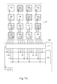
- FIG. 4A to FIG. 7A and FIG. 4B to FIG. 7B are diagrams of verification apparatus 100 suitable for touch display panel 200 according to different embodiments of the disclosure.
- a touch display panel 400 includes divided partitions 401 ⁇ 416 .
- Divided partitions 401 , 403 , 405 , 407 , 409 , 411 , 413 , 415 are arranged on odd rows of the touch display panel 400
- divided partitions 402 , 404 , 406 , 408 , 410 , 412 , 414 , 416 are arranged on even rows of the 400 .
- the signal generating circuit 130 When the signal generating circuit 130 simultaneously sends the verification voltages V 1 and V 2 respectively to the divided partitions on the odd and even rows.
- the brightness of the divided partitions on the odd rows are the same, and the brightness of the divided partitions on the even rows are also the same but different from that of the odd rows.
- Step S 308 is executed to adjust the control signal CS generated by the control circuit 110 to low-logic level to turn off the switch units in the verification switch circuit 120 , then the verification voltages V 1 and V 2 will not be sent to the divided partitions 401 ⁇ 416 of the touch display panel 400 .
- Another circuit (that is, the working circuit) takes over the control of the divided partitions in step S 310 .
- the divided partition 410 on the even row displays at the same brightness with the divided partitions 409 and 411 on the odd rows. It can be observed that there is a short circuit between divided partition 410 and divided partition 409 or 411 , and in this situation, the flow will return to step S 302 to send the verification voltages V 1 and V 2 again to confirm the function of the touch display panel.
- the above embodiment can be used to confirm whether there is a short circuit between the up and down adjacent divided partitions. Nonetheless, by this method, whether there is a short circuit between divided partitions in odd and even rows or between left and right adjacent divided partitions cannot be validated.
- a touch display panel 400 includes divided partitions 401 ⁇ 416 .
- Divided partitions 401 , 402 , 403 , 404 , 409 , 410 , 411 , 412 are arranged on odd columns of the touch display panel 400 , and divided partitions 405 , 406 , 407 , 408 , 413 , 414 , 415 , 416 are arranged on even columns of the 400 .
- the signal generating circuit 130 When the signal generating circuit 130 simultaneously send the verification voltages V 1 and V 2 respectively to the divided partitions on the odd and even columns.
- the brightness of the divided partitions on the odd columns are the same, and the brightness of the divided partitions on the even columns are also the same but different from that of the odd columns.
- the left and right adjacent divided partitions of the touch display panel 400 have no short circuit.
- the divided partition 412 on the even column displays at the same brightness with the divided partitions 408 and 416 on the odd columns. It can be observed that there is a short circuit between divided partition 412 and divided partition 408 or 416 .
- the above embodiment can be used to confirm whether there is a short circuit between the left and right adjacent divided partitions. Nonetheless, by this method, whether there is a short circuit between divided partitions in odd and even columns or between up and down adjacent divided partitions cannot be validated.
- a touch display panel 400 includes divided partitions 401 ⁇ 416 .
- Divided partitions 401 , 402 , 403 , 404 , 409 , 410 , 411 , 412 are arranged on odd columns of the touch display panel 400 , and divided partitions 405 , 406 , 407 , 408 , 413 , 414 , 415 , 416 are arranged on even columns of the 400 .
- the signal generating circuit 130 alternately sends the verification voltages to every two adjacent divided partitions on the odd columns via the circuit switch units in the verification switch circuit 120 .
- the so-called alternately sends the verification voltages to every two adjacent divided partitions indicates that, as shown in FIG. 6A , for the divided partitions 401 ⁇ 404 in odd column, send verification voltages V 1 and V 2 to adjacent divided partitions 401 and 402 , and simultaneously send verification voltages V 1 and V 2 to adjacent divided partitions 403 and 404 .
- the divided partitions 405 ⁇ 408 in even column send verification voltages V 2 and V 1 to adjacent divided partitions 405 and 406 , and simultaneously send verification voltages V 2 and V 1 to adjacent divided partitions 407 and 408 .
- any arbitrary adjacent divided partitions in odd and even columns receive different verification voltage.
- the divided partition 401 on the odd column and the divided partition 405 on the even column receive verification voltages V 1 and V 2 respectively.
- the divided partition 402 on the odd column and the divided partition 406 on the even column receive verification voltages V 2 and V 1 respectively.
- the brightness of an arbitrary divided partition on the odd or even column is different from its neighbors in four directions. If this is true, it can be confirmed that there is no short circuit between the divided partition and its neighbors in four directions.
- the brightness of the divided partition 407 on the even column is different from the brightness of the divided partition 406 (i.e., the partition adjacent to the divided partition 407 on the top side) and the brightness of the divided partition 408 (i.e., the partition adjacent to the divided partition 407 on the bottom side).
- the brightness of the divided partition 407 is different from the brightness of the divided partition 403 (i.e., the partition adjacent to the divided partition 407 on the left side) and the divided partition 411 (i.e., the partition adjacent to the divided partition 407 on the right side). Then there is no short circuit between the divided partition 407 and the divided partitions 406 / 408 / 403 / 411 in the neighborhood along four directions.
- the brightness of the divided partition 410 on the even column is different from the brightness of the upside/downside adjacent divided partitions 409 and 411 .
- the brightness of the divided partition 410 is different from the brightness of the leftside/rightside adjacent divided partitions 406 and 414 . Then there is no short circuit between the divided partition 410 and the neighboring divided partitions 409 , 411 , 406 , and 414 in four directions.
- the brightness of the divided partition 407 on even column is the same as the divided partitions 403 and 411 on odd column and the divided partitions 406 and 408 on even column. It can be judged that there is a short circuit between the divided partition 407 and one of the divided partitions 403 , 406 , 408 , and 411 . Comparing to the embodiments shown in FIG. 4A to FIG. 4B and FIG. 5A to FIG. 5B above, whether there is a short circuit between an arbitrary divided partition and the neighbors in four directions can be verified simultaneously in this embodiment.
- step S 306 the control signal CS generated by the control circuit 110 is adjusted to low-logic level (such as 0).
- the switch units in the verification switch circuit 120 is turned off, and the sending of verification voltages from the signal generating circuit 130 to the divided partitions 401 ⁇ 416 of the touch display panel 400 is stopped.
- another circuit (which is the working circuit) will replace the verification apparatus 100 , and control the divided partitions 401 ⁇ 416 of the touch display panel 400 separately.
- the mechanism of how the working circuit controls touch display panel is the same as it is mentioned previously.
- the signal generating circuit 130 sends verification voltages V 1 , V 2 , V 3 , and V 4 via the circuit switch units in the verification switch circuit 120 to four adjacent divided partitions on the odd column. That is, send the verification voltage V 1 , V 2 , V 3 , and V 4 to divided partitions 401 , 402 , 403 , and 404 . Also, send the verification voltage V 4 , V 1 , V 2 , and V 3 to divided partitions 405 , 406 , 407 , and 408 .
- this disclosure provides a verification apparatus.
- the verification apparatus By using the verification apparatus, light-emitting verification and short circuit verification for the divided partitions of the touch display panel can be conducted.
Landscapes
- Engineering & Computer Science (AREA)
- Theoretical Computer Science (AREA)
- General Engineering & Computer Science (AREA)
- Physics & Mathematics (AREA)
- General Physics & Mathematics (AREA)
- Human Computer Interaction (AREA)
- Computer Hardware Design (AREA)
- Liquid Crystal (AREA)
- Control Of Indicators Other Than Cathode Ray Tubes (AREA)
- Position Input By Displaying (AREA)
Abstract
Description
Claims (4)
Applications Claiming Priority (3)
| Application Number | Priority Date | Filing Date | Title |
|---|---|---|---|
| CN201610004021.XA CN106940975A (en) | 2016-01-04 | 2016-01-04 | Detection device and detection method |
| CN201610004021.X | 2016-01-04 | ||
| CN201610004021 | 2016-01-04 |
Publications (2)
| Publication Number | Publication Date |
|---|---|
| US20170192606A1 US20170192606A1 (en) | 2017-07-06 |
| US10175820B2 true US10175820B2 (en) | 2019-01-08 |
Family
ID=59226273
Family Applications (1)
| Application Number | Title | Priority Date | Filing Date |
|---|---|---|---|
| US15/080,540 Active - Reinstated 2037-06-09 US10175820B2 (en) | 2016-01-04 | 2016-03-24 | Verification apparatus and verification method for touch display panel |
Country Status (3)
| Country | Link |
|---|---|
| US (1) | US10175820B2 (en) |
| CN (1) | CN106940975A (en) |
| TW (1) | TW201734987A (en) |
Families Citing this family (5)
| Publication number | Priority date | Publication date | Assignee | Title |
|---|---|---|---|---|
| CN106782255A (en) * | 2017-03-23 | 2017-05-31 | 京东方科技集团股份有限公司 | One kind detection circuit, detection method and detection means |
| CN107742505B (en) * | 2017-10-26 | 2019-11-05 | 惠科股份有限公司 | Display device |
| CN108983461B (en) * | 2018-08-22 | 2021-04-27 | 惠科股份有限公司 | Array substrate and liquid crystal module |
| CN109522170B (en) * | 2018-11-15 | 2022-03-25 | 北京小米移动软件有限公司 | Front shell display module detection device and system |
| TWI701583B (en) * | 2019-01-23 | 2020-08-11 | 友達光電股份有限公司 | Integrated touch panel and test method thereof |
Citations (4)
| Publication number | Priority date | Publication date | Assignee | Title |
|---|---|---|---|---|
| US20050057487A1 (en) * | 2003-09-11 | 2005-03-17 | Haruki Takata | Display system and display panel and signal processing apparatus for use with display system |
| TWI365318B (en) | 2008-06-17 | 2012-06-01 | Au Optronics Corp | Detection circuit and method for lcd panel |
| US20120147664A1 (en) * | 2010-12-08 | 2012-06-14 | Hynix Semiconductor Inc. | Non-volatile memory device and method for controlling the same |
| US20140375344A1 (en) | 2013-06-20 | 2014-12-25 | Shenzhen China Star Optoelectronics Technology Co., Ltd. | Liquid crystal panel, and testing circuit and testing method thereof |
Family Cites Families (6)
| Publication number | Priority date | Publication date | Assignee | Title |
|---|---|---|---|---|
| CN1251170C (en) * | 2002-07-23 | 2006-04-12 | 李友端 | Touch type liquid crystal display and touch method thereof |
| CN102455960B (en) * | 2010-10-28 | 2016-03-16 | 上海天马微电子有限公司 | Detection device and detection method |
| KR102043299B1 (en) * | 2012-12-26 | 2019-11-11 | 엘지디스플레이 주식회사 | Touch Screen With Integrated Display Device And Method for Testing of Touch Panel |
| CN104793829B (en) * | 2015-05-08 | 2018-01-26 | 厦门天马微电子有限公司 | A touch device, driving method, array substrate and liquid crystal display panel |
| CN105093593B (en) * | 2015-09-11 | 2018-10-30 | 京东方科技集团股份有限公司 | Display base plate and its test method, display device |
| CN105975129B (en) * | 2016-05-04 | 2018-08-28 | 厦门天马微电子有限公司 | Display panel and its test method, application method |
-
2016
- 2016-01-04 CN CN201610004021.XA patent/CN106940975A/en active Pending
- 2016-03-24 US US15/080,540 patent/US10175820B2/en active Active - Reinstated
- 2016-12-13 TW TW105141499A patent/TW201734987A/en unknown
Patent Citations (4)
| Publication number | Priority date | Publication date | Assignee | Title |
|---|---|---|---|---|
| US20050057487A1 (en) * | 2003-09-11 | 2005-03-17 | Haruki Takata | Display system and display panel and signal processing apparatus for use with display system |
| TWI365318B (en) | 2008-06-17 | 2012-06-01 | Au Optronics Corp | Detection circuit and method for lcd panel |
| US20120147664A1 (en) * | 2010-12-08 | 2012-06-14 | Hynix Semiconductor Inc. | Non-volatile memory device and method for controlling the same |
| US20140375344A1 (en) | 2013-06-20 | 2014-12-25 | Shenzhen China Star Optoelectronics Technology Co., Ltd. | Liquid crystal panel, and testing circuit and testing method thereof |
Also Published As
| Publication number | Publication date |
|---|---|
| CN106940975A (en) | 2017-07-11 |
| TW201734987A (en) | 2017-10-01 |
| US20170192606A1 (en) | 2017-07-06 |
Similar Documents
| Publication | Publication Date | Title |
|---|---|---|
| US10175820B2 (en) | Verification apparatus and verification method for touch display panel | |
| KR102573208B1 (en) | Display panel | |
| KR101487700B1 (en) | Display device and method of driving the same | |
| CN112925448B (en) | Touch display panel, detection method thereof and touch display device | |
| JP6358935B2 (en) | Display device and touch detection method | |
| CN106909253B (en) | Touch display panel and touch display device | |
| US10825374B2 (en) | Liquid crystal drive circuit, backlight circuit, terminal, device and method | |
| CN110716665B (en) | Touch display panel and display device | |
| CN110688030B (en) | Touch display panel and display device | |
| KR102133736B1 (en) | Display device with integrated touch screen and method for driving the same | |
| US10388209B2 (en) | Interface circuit | |
| KR102242104B1 (en) | Display device | |
| KR102884505B1 (en) | Touch circuit, touch display device, and touch driving method thereof | |
| JP2005352572A (en) | Coordinate input device | |
| KR20170084398A (en) | Display device and driving method thereof | |
| KR20170036501A (en) | Display panel and display apparatus using the same | |
| US11990103B2 (en) | Interface circuit, source driver, and display device | |
| KR102595502B1 (en) | Touch panel and inspection method of thereof, and liquid crystal display device having touch panel | |
| CN110232888A (en) | A kind of driving method of display panel, display device and display device | |
| US9727169B2 (en) | Embedded display screen having touch detection function, terminal device, and touch detection method | |
| KR101314863B1 (en) | Display device and driving method thereof | |
| CN106909008B (en) | Array substrate, display panel and detection method of display panel | |
| KR102544983B1 (en) | Test system and test controller | |
| CN115346473A (en) | Display panel, driving circuit and driving method | |
| CN106228930B (en) | Display device |
Legal Events
| Date | Code | Title | Description |
|---|---|---|---|
| AS | Assignment |
Owner name: CHUNGHWA PICTURE TUBES, LTD., TAIWAN Free format text: ASSIGNMENT OF ASSIGNORS INTEREST;ASSIGNORS:CHANG, SHAO-LUN;WENG, CHANG-SHENG;KUO, CHI-LIANG;AND OTHERS;REEL/FRAME:038097/0972 Effective date: 20160324 |
|
| STCF | Information on status: patent grant |
Free format text: PATENTED CASE |
|
| FEPP | Fee payment procedure |
Free format text: MAINTENANCE FEE REMINDER MAILED (ORIGINAL EVENT CODE: REM.); ENTITY STATUS OF PATENT OWNER: LARGE ENTITY |
|
| LAPS | Lapse for failure to pay maintenance fees |
Free format text: PATENT EXPIRED FOR FAILURE TO PAY MAINTENANCE FEES (ORIGINAL EVENT CODE: EXP.); ENTITY STATUS OF PATENT OWNER: LARGE ENTITY |
|
| PRDP | Patent reinstated due to the acceptance of a late maintenance fee |
Effective date: 20230306 |
|
| FEPP | Fee payment procedure |
Free format text: PETITION RELATED TO MAINTENANCE FEES FILED (ORIGINAL EVENT CODE: PMFP); ENTITY STATUS OF PATENT OWNER: LARGE ENTITY Free format text: PETITION RELATED TO MAINTENANCE FEES GRANTED (ORIGINAL EVENT CODE: PMFG); ENTITY STATUS OF PATENT OWNER: LARGE ENTITY Free format text: SURCHARGE, PETITION TO ACCEPT PYMT AFTER EXP, UNINTENTIONAL (ORIGINAL EVENT CODE: M1558); ENTITY STATUS OF PATENT OWNER: LARGE ENTITY |
|
| MAFP | Maintenance fee payment |
Free format text: PAYMENT OF MAINTENANCE FEE, 4TH YEAR, LARGE ENTITY (ORIGINAL EVENT CODE: M1551); ENTITY STATUS OF PATENT OWNER: LARGE ENTITY Year of fee payment: 4 |
|
| STCF | Information on status: patent grant |
Free format text: PATENTED CASE |
|
| FP | Lapsed due to failure to pay maintenance fee |
Effective date: 20230108 |