US10164063B2 - Semiconductor structure with protection layer - Google Patents
Semiconductor structure with protection layer Download PDFInfo
- Publication number
- US10164063B2 US10164063B2 US15/434,343 US201715434343A US10164063B2 US 10164063 B2 US10164063 B2 US 10164063B2 US 201715434343 A US201715434343 A US 201715434343A US 10164063 B2 US10164063 B2 US 10164063B2
- Authority
- US
- United States
- Prior art keywords
- layer
- protection layer
- forming
- gate dielectric
- over
- Prior art date
- Legal status (The legal status is an assumption and is not a legal conclusion. Google has not performed a legal analysis and makes no representation as to the accuracy of the status listed.)
- Active
Links
Images


Classifications
-
- H01L29/66795—
-
- H—ELECTRICITY
- H10—SEMICONDUCTOR DEVICES; ELECTRIC SOLID-STATE DEVICES NOT OTHERWISE PROVIDED FOR
- H10D—INORGANIC ELECTRIC SEMICONDUCTOR DEVICES
- H10D30/00—Field-effect transistors [FET]
- H10D30/01—Manufacture or treatment
- H10D30/021—Manufacture or treatment of FETs having insulated gates [IGFET]
- H10D30/024—Manufacture or treatment of FETs having insulated gates [IGFET] of fin field-effect transistors [FinFET]
-
- H01L21/823431—
-
- H01L21/82345—
-
- H01L21/823456—
-
- H01L21/823462—
-
- H01L21/823468—
-
- H01L27/088—
-
- H01L27/0886—
-
- H01L29/42364—
-
- H01L29/4983—
-
- H01L29/66545—
-
- H01L29/6656—
-
- H01L29/785—
-
- H—ELECTRICITY
- H10—SEMICONDUCTOR DEVICES; ELECTRIC SOLID-STATE DEVICES NOT OTHERWISE PROVIDED FOR
- H10D—INORGANIC ELECTRIC SEMICONDUCTOR DEVICES
- H10D30/00—Field-effect transistors [FET]
- H10D30/60—Insulated-gate field-effect transistors [IGFET]
- H10D30/62—Fin field-effect transistors [FinFET]
- H10D30/6211—Fin field-effect transistors [FinFET] having fin-shaped semiconductor bodies integral with the bulk semiconductor substrates
-
- H—ELECTRICITY
- H10—SEMICONDUCTOR DEVICES; ELECTRIC SOLID-STATE DEVICES NOT OTHERWISE PROVIDED FOR
- H10D—INORGANIC ELECTRIC SEMICONDUCTOR DEVICES
- H10D64/00—Electrodes of devices having potential barriers
- H10D64/01—Manufacture or treatment
- H10D64/017—Manufacture or treatment using dummy gates in processes wherein at least parts of the final gates are self-aligned to the dummy gates, i.e. replacement gate processes
-
- H—ELECTRICITY
- H10—SEMICONDUCTOR DEVICES; ELECTRIC SOLID-STATE DEVICES NOT OTHERWISE PROVIDED FOR
- H10D—INORGANIC ELECTRIC SEMICONDUCTOR DEVICES
- H10D64/00—Electrodes of devices having potential barriers
- H10D64/01—Manufacture or treatment
- H10D64/021—Manufacture or treatment using multiple gate spacer layers, e.g. bilayered sidewall spacers
-
- H—ELECTRICITY
- H10—SEMICONDUCTOR DEVICES; ELECTRIC SOLID-STATE DEVICES NOT OTHERWISE PROVIDED FOR
- H10D—INORGANIC ELECTRIC SEMICONDUCTOR DEVICES
- H10D64/00—Electrodes of devices having potential barriers
- H10D64/20—Electrodes characterised by their shapes, relative sizes or dispositions
- H10D64/27—Electrodes not carrying the current to be rectified, amplified, oscillated or switched, e.g. gates
- H10D64/311—Gate electrodes for field-effect devices
- H10D64/411—Gate electrodes for field-effect devices for FETs
- H10D64/511—Gate electrodes for field-effect devices for FETs for IGFETs
- H10D64/514—Gate electrodes for field-effect devices for FETs for IGFETs characterised by the insulating layers
-
- H—ELECTRICITY
- H10—SEMICONDUCTOR DEVICES; ELECTRIC SOLID-STATE DEVICES NOT OTHERWISE PROVIDED FOR
- H10D—INORGANIC ELECTRIC SEMICONDUCTOR DEVICES
- H10D64/00—Electrodes of devices having potential barriers
- H10D64/60—Electrodes characterised by their materials
- H10D64/66—Electrodes having a conductor capacitively coupled to a semiconductor by an insulator, e.g. MIS electrodes
- H10D64/667—Electrodes having a conductor capacitively coupled to a semiconductor by an insulator, e.g. MIS electrodes the conductor comprising a layer of alloy material, compound material or organic material contacting the insulator, e.g. TiN workfunction layers
-
- H—ELECTRICITY
- H10—SEMICONDUCTOR DEVICES; ELECTRIC SOLID-STATE DEVICES NOT OTHERWISE PROVIDED FOR
- H10D—INORGANIC ELECTRIC SEMICONDUCTOR DEVICES
- H10D64/00—Electrodes of devices having potential barriers
- H10D64/60—Electrodes characterised by their materials
- H10D64/66—Electrodes having a conductor capacitively coupled to a semiconductor by an insulator, e.g. MIS electrodes
- H10D64/671—Electrodes having a conductor capacitively coupled to a semiconductor by an insulator, e.g. MIS electrodes the conductor having lateral variation in doping or structure
-
- H—ELECTRICITY
- H10—SEMICONDUCTOR DEVICES; ELECTRIC SOLID-STATE DEVICES NOT OTHERWISE PROVIDED FOR
- H10D—INORGANIC ELECTRIC SEMICONDUCTOR DEVICES
- H10D84/00—Integrated devices formed in or on semiconductor substrates that comprise only semiconducting layers, e.g. on Si wafers or on GaAs-on-Si wafers
- H10D84/01—Manufacture or treatment
- H10D84/0123—Integrating together multiple components covered by H10D12/00 or H10D30/00, e.g. integrating multiple IGBTs
- H10D84/0126—Integrating together multiple components covered by H10D12/00 or H10D30/00, e.g. integrating multiple IGBTs the components including insulated gates, e.g. IGFETs
- H10D84/0135—Manufacturing their gate conductors
- H10D84/014—Manufacturing their gate conductors the gate conductors having different materials or different implants
-
- H—ELECTRICITY
- H10—SEMICONDUCTOR DEVICES; ELECTRIC SOLID-STATE DEVICES NOT OTHERWISE PROVIDED FOR
- H10D—INORGANIC ELECTRIC SEMICONDUCTOR DEVICES
- H10D84/00—Integrated devices formed in or on semiconductor substrates that comprise only semiconducting layers, e.g. on Si wafers or on GaAs-on-Si wafers
- H10D84/01—Manufacture or treatment
- H10D84/0123—Integrating together multiple components covered by H10D12/00 or H10D30/00, e.g. integrating multiple IGBTs
- H10D84/0126—Integrating together multiple components covered by H10D12/00 or H10D30/00, e.g. integrating multiple IGBTs the components including insulated gates, e.g. IGFETs
- H10D84/0135—Manufacturing their gate conductors
- H10D84/0142—Manufacturing their gate conductors the gate conductors having different shapes or dimensions
-
- H—ELECTRICITY
- H10—SEMICONDUCTOR DEVICES; ELECTRIC SOLID-STATE DEVICES NOT OTHERWISE PROVIDED FOR
- H10D—INORGANIC ELECTRIC SEMICONDUCTOR DEVICES
- H10D84/00—Integrated devices formed in or on semiconductor substrates that comprise only semiconducting layers, e.g. on Si wafers or on GaAs-on-Si wafers
- H10D84/01—Manufacture or treatment
- H10D84/0123—Integrating together multiple components covered by H10D12/00 or H10D30/00, e.g. integrating multiple IGBTs
- H10D84/0126—Integrating together multiple components covered by H10D12/00 or H10D30/00, e.g. integrating multiple IGBTs the components including insulated gates, e.g. IGFETs
- H10D84/0144—Manufacturing their gate insulating layers
-
- H—ELECTRICITY
- H10—SEMICONDUCTOR DEVICES; ELECTRIC SOLID-STATE DEVICES NOT OTHERWISE PROVIDED FOR
- H10D—INORGANIC ELECTRIC SEMICONDUCTOR DEVICES
- H10D84/00—Integrated devices formed in or on semiconductor substrates that comprise only semiconducting layers, e.g. on Si wafers or on GaAs-on-Si wafers
- H10D84/01—Manufacture or treatment
- H10D84/0123—Integrating together multiple components covered by H10D12/00 or H10D30/00, e.g. integrating multiple IGBTs
- H10D84/0126—Integrating together multiple components covered by H10D12/00 or H10D30/00, e.g. integrating multiple IGBTs the components including insulated gates, e.g. IGFETs
- H10D84/0147—Manufacturing their gate sidewall spacers
-
- H—ELECTRICITY
- H10—SEMICONDUCTOR DEVICES; ELECTRIC SOLID-STATE DEVICES NOT OTHERWISE PROVIDED FOR
- H10D—INORGANIC ELECTRIC SEMICONDUCTOR DEVICES
- H10D84/00—Integrated devices formed in or on semiconductor substrates that comprise only semiconducting layers, e.g. on Si wafers or on GaAs-on-Si wafers
- H10D84/01—Manufacture or treatment
- H10D84/0123—Integrating together multiple components covered by H10D12/00 or H10D30/00, e.g. integrating multiple IGBTs
- H10D84/0126—Integrating together multiple components covered by H10D12/00 or H10D30/00, e.g. integrating multiple IGBTs the components including insulated gates, e.g. IGFETs
- H10D84/0158—Integrating together multiple components covered by H10D12/00 or H10D30/00, e.g. integrating multiple IGBTs the components including insulated gates, e.g. IGFETs the components including FinFETs
-
- H—ELECTRICITY
- H10—SEMICONDUCTOR DEVICES; ELECTRIC SOLID-STATE DEVICES NOT OTHERWISE PROVIDED FOR
- H10D—INORGANIC ELECTRIC SEMICONDUCTOR DEVICES
- H10D84/00—Integrated devices formed in or on semiconductor substrates that comprise only semiconducting layers, e.g. on Si wafers or on GaAs-on-Si wafers
- H10D84/01—Manufacture or treatment
- H10D84/02—Manufacture or treatment characterised by using material-based technologies
- H10D84/03—Manufacture or treatment characterised by using material-based technologies using Group IV technology, e.g. silicon technology or silicon-carbide [SiC] technology
- H10D84/038—Manufacture or treatment characterised by using material-based technologies using Group IV technology, e.g. silicon technology or silicon-carbide [SiC] technology using silicon technology, e.g. SiGe
-
- H—ELECTRICITY
- H10—SEMICONDUCTOR DEVICES; ELECTRIC SOLID-STATE DEVICES NOT OTHERWISE PROVIDED FOR
- H10D—INORGANIC ELECTRIC SEMICONDUCTOR DEVICES
- H10D84/00—Integrated devices formed in or on semiconductor substrates that comprise only semiconducting layers, e.g. on Si wafers or on GaAs-on-Si wafers
- H10D84/80—Integrated devices formed in or on semiconductor substrates that comprise only semiconducting layers, e.g. on Si wafers or on GaAs-on-Si wafers characterised by the integration of at least one component covered by groups H10D12/00 or H10D30/00, e.g. integration of IGFETs
- H10D84/82—Integrated devices formed in or on semiconductor substrates that comprise only semiconducting layers, e.g. on Si wafers or on GaAs-on-Si wafers characterised by the integration of at least one component covered by groups H10D12/00 or H10D30/00, e.g. integration of IGFETs of only field-effect components
- H10D84/83—Integrated devices formed in or on semiconductor substrates that comprise only semiconducting layers, e.g. on Si wafers or on GaAs-on-Si wafers characterised by the integration of at least one component covered by groups H10D12/00 or H10D30/00, e.g. integration of IGFETs of only field-effect components of only insulated-gate FETs [IGFET]
- H10D84/834—Integrated devices formed in or on semiconductor substrates that comprise only semiconducting layers, e.g. on Si wafers or on GaAs-on-Si wafers characterised by the integration of at least one component covered by groups H10D12/00 or H10D30/00, e.g. integration of IGFETs of only field-effect components of only insulated-gate FETs [IGFET] comprising FinFETs
Definitions
- Semiconductor devices are used in a variety of electronic applications, such as personal computers, cell phones, digital cameras, and other electronic equipment. Semiconductor devices are typically fabricated by sequentially depositing insulating or dielectric layers, conductive layers, and semiconductor layers of material over a semiconductor substrate, and patterning the various material layers using lithography to form circuit components and elements thereon.
- Semiconductor devices may include core devices and input/output devices.
- the core devices may be used to perform the functions of a chip, and the input/output devices may be used to communicate with external circuits in other chips.
- existing manufacturing processes for these semiconductor devices have generally been adequate for their intended purposes, as device scaling-down continues, they have not been entirely satisfactory in all respects.
- FIGS. 1A to 1J are perspective representations of various stages of forming a semiconductor structure in accordance with some embodiments.
- FIG. 2 is a cross-sectional representation of the semiconductor structure shown alone line A-A′ in FIG. 1J in accordance with some embodiments.
- FIGS. 3A to 3I are cross-sectional representations of various stages of forming a semiconductor structure in accordance with some embodiments.
- first and second features are formed in direct contact
- additional features may be formed between the first and second features, such that the first and second features may not be in direct contact
- present disclosure may repeat reference numerals and/or letters in the various examples. This repetition is for the purpose of simplicity and clarity and does not in itself dictate a relationship between the various embodiments and/or configurations discussed.
- spatially relative terms such as “beneath,” “below,” “lower,” “above,” “upper” and the like, may be used herein for ease of description to describe one element or feature's relationship to another element(s) or feature(s) as illustrated in the figures.
- the spatially relative terms are intended to encompass different orientations of the device in use or operation in addition to the orientation depicted in the figures.
- the apparatus may be otherwise oriented (rotated 90 degrees or at other orientations) and the spatially relative descriptors used herein may likewise be interpreted accordingly. It should be understood that additional operations can be provided before, during, and after the method, and some of the operations described can be replaced or eliminated for other embodiments of the method.
- Embodiments of semiconductor structures and methods for forming the same are provided.
- the method for forming the semiconductor structure may include forming a protection layer over a substrate before a dummy gate layer is formed, so that the protection layer may protect the substrate during the process of patterning the dummy gate layer.
- the protection layer may be relatively thick to provide better protection for the substrate and may be removed afterwards, so that the performance of the resulting semiconductor structure may be improved.
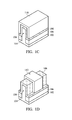
- FIGS. 1A to 1J are perspective representations of various stages of forming a semiconductor structure 100 in accordance with some embodiments.
- a substrate 102 is provided in accordance with some embodiments.
- the substrate 102 may be a semiconductor wafer such as a silicon wafer.
- the substrate 102 may include elementary semiconductor materials, compound semiconductor materials, and/or alloy semiconductor materials.
- the elementary semiconductor materials may include, but are not limited to, crystal silicon, polycrystalline silicon, amorphous silicon, germanium, and diamond.
- the compound semiconductor materials may include, but are not limited to, silicon carbide, gallium arsenic, gallium phosphide, indium phosphide, indium arsenide, and indium antimonide.
- the alloy semiconductor materials may include, but are not limited to, SiGe, GaAsP, AlInAs, AlGaAs, GaInAs, GaInP, and GaInAsP.
- a fin structure 104 is formed from the substrate 102 , and an isolation structure 106 is formed around the fin structure 104 , as shown in FIG. 1A in accordance with some embodiments.
- the fin structure 104 may be formed by patterning the substrate 102 .
- the isolation structure 106 may be formed by forming an insulating material over the substrate 102 and the fin structure 104 and recessing the insulating material to expose the top portion of the fin structure 104 .
- the insulating material is made of silicon oxide, silicon nitride, silicon oxynitride, fluoride-doped silicate glass (FSG), or other low-K dielectric materials.
- the insulating material may be formed by using a high-density-plasma (HDP) CVD process, although other deposition processes may be used in other embodiments.
- HDP high-density-plasma
- a protection layer 108 is formed over the fin structure 104 and the isolation structure 106 , as shown in FIG. 1B in accordance with some embodiments.
- the protection layer 108 is formed over the top surface of the sidewalls of the fin structure 104 and extends over the top surface of the isolation structure 106 .
- the protection layer 108 may be configured to prevent the substrate 102 and the elements formed over the substrate (e.g. the fin structure 104 and the isolation structure 106 ) from being damaged in subsequent manufacturing processes, and therefore the protection layer 108 may be relatively thick to protect the elements below it.
- the protection layer 108 has a thickness in a range from about 20 ⁇ to about 100 ⁇ .
- the protection layer 108 should be thick enough to protect the structure formed below it, while not being too thick or it may be too difficult to be completely removed and therefore undermine the performance of the resulting semiconductor structure.
- the protection layer 108 is an oxide layer. In some embodiments, the protection layer 108 is a silicon oxide layer. In some embodiments, the protection layer 108 is made of metal oxides, metal nitrides, metal silicates, transition metal-oxides, transition metal-nitrides, transition metal-silicates, or oxynitrides of metals.
- Examples of materials used to form the protection layer 108 include, but are not limited to, hafnium oxide (HfO 2 ), hafnium silicon oxide (HfSiO), hafnium silicon oxynitride (HfSiON), hafnium tantalum oxide (HfTaO), hafnium titanium oxide (HfTiO), hafnium zirconium oxide (HfZrO), silicon nitride, silicon oxynitride, zirconium oxide, titanium oxide, aluminum oxide, hafnium dioxide-alumina (HfO 2 —Al 2 O 3 ) alloy, or other applicable dielectric materials.
- hafnium oxide HfO 2
- hafnium silicon oxide HfSiO
- hafnium silicon oxynitride HfSiON
- hafTaO hafnium titanium oxide
- HfZrO hafnium zirconium oxide
- silicon nitride silicon oxynitride
- a dummy gate layer 110 is formed over the protection layer 108 , as shown in FIG. 1C in accordance with some embodiments.
- the dummy gate layer 110 is a polysilicon layer.
- the dummy gate layer 110 is patterned to form a dummy gate structure 112 , as shown in FIG. 1D in accordance with some embodiments.
- the dummy gate layer 110 may be patterned by forming a mask over a portion of the dummy gate layer 110 and etching the portions of the dummy gate layer 110 not covered by the mask.
- the dummy gate layer 110 may be etched by performing a dry etching process. The dry etching process may be designed to be stopped when the protection layer 108 is exposed.
- the protection layer 108 is relatively thick, so that even if some top portions of the protection layer 108 are removed during the etching process, the structure formed underneath (e.g. the fin structure 104 and/or the isolation structure 106 ) can still be well protected and therefore will not be damaged.
- spacers 114 are formed on the sidewalls of the dummy gate structure 112 , as shown in FIG. 1E in accordance with some embodiments. In addition, the spacers 114 also cover portions of the protection layer 108 .
- the protection layer 108 includes a first portion 108 i , second portions 108 ii , and third portions 108 iii , and the dummy gate structure 112 is located over a first portion 108 i of the protection layer 108 and the spacers 114 are formed over the second portions 108 ii of the protection layer 108 .
- the second portions 108 ii of the protection layer 108 are located at the opposite sides of the first portion 108 i of the protection layer 108
- the third portions 108 iii are further apart from the first portion 108 i of the protection layer 108 .
- the spacers 114 are made of silicon nitride, silicon oxide, silicon oxynitride, silicon carbide, or other applicable dielectric materials. In some embodiments, the spacers 114 and the protection layer 108 are made of different materials so that they may have relatively good etching selectivity in subsequent etching processes.
- the exposed portions of the protection layer 108 are removed, as shown in FIG. 1F in accordance with some embodiments. That is, the third portions 108 iii of the protection layer 108 not covered by the dummy gate structure 112 and the spacers 114 are removed. In some embodiments, the third portions 108 iii of the protection layer 108 are removed by performing an etching process.
- source/drain structures 116 are formed in the fin structure 104 adjacent to the dummy gate structure 112 , as shown in FIG. 1F in accordance with some embodiments.
- the source/drain structures 116 are formed at opposite sides of the dummy gate structure 112 in accordance with some embodiments.
- the source/drain structures 116 may be formed by recessing the fin structure 104 and growing semiconductor materials in the recesses by performing epitaxial (epi) processes.
- the source/drain structures 116 include Ge, SiGe, InAs, InGaAs, InSb, GaAs, GaSb, InAlP, InP, or a combination thereof.
- a contact etch stop layer (CESL) 118 is formed over substrate 102 , and an interlayer dielectric layer 120 is formed over the contact etch stop layer 118 , as shown in FIG. 1H in accordance with some embodiments.
- the contact etch stop layer 118 is made of silicon nitride, silicon oxynitride, and/or other applicable materials.
- the contact etch stop layer 118 may be formed by performing plasma enhanced CVD, low pressure CVD, ALD, or other applicable processes.
- the interlayer dielectric layer 120 may include multilayers made of multiple dielectric materials, such as silicon oxide, silicon nitride, silicon oxynitride, phosphosilicate glass (PSG), borophosphosilicate glass (BPSG), and/or other applicable low-k dielectric materials.
- the interlayer dielectric layer 236 may be formed by performing chemical vapor deposition (CVD), physical vapor deposition, (PVD), atomic layer deposition (ALD), spin-on coating, or other applicable processes.
- the dummy gate structure 112 is removed to form a trench 122 between the spacers 114 , as shown in FIG. 1H in accordance with some embodiments.
- the dummy gate structure 112 is removed by performing a dry etching process. As shown in FIG. 1H , after the dummy gate structure 112 is removed, the first portion 108 i of the protection layer 108 is exposed by the trench 122 while the second portions 108 ii of the protection layer 108 are covered by the spacers 114 .
- the first portion 108 i of the protection layer 108 exposed by the trench 122 is removed, as shown in FIG. 1I in accordance with some embodiments.
- the first portion 108 i of the protection layer 108 is removed by performing a dry etching process.
- some portions of the fin structure 104 and the isolation structure 106 are exposed by the trench 122 after the first portion 108 i of the protection layer 108 is removed.
- a metal gate structure 124 is formed in the trench 122 , as shown in FIG. 1J in accordance with some embodiments.
- the metal gate structure 124 in the semiconductor structure 100 includes a gate dielectric layer 126 , a work function metal layer 128 , and a gate electrode layer 130 . Since the first portion 108 i of the protection layer 108 is removed before the metal gate structure 124 is formed, the metal gate structure 124 is formed directly on the fin structure 104 and the isolation structure 106 .
- the gate dielectric layer 126 and the protection layer 108 are made of the same material, but the protection layer 108 is thicker than the gate dielectric layer 126 .
- the protection layer 108 is formed to protect the structures under it (e.g. the fin structure 104 and the isolation structure 106 ) during subsequent etching processes. Therefore, the protection layer 108 is designed to be relatively thick.
- the thickness of the gate dielectric layer 126 is designed to be relatively thin, so that the resulting semiconductor structure 100 may have a lower resistance.
- the difference between the thickness of the protection layer 108 and the thickness of the gate dielectric layer 126 is in a range from about 5 ⁇ to about 80 ⁇ . As described above, the difference of the thicknesses between the protection layer 108 and the gate dielectric layer 126 is adjusted, so that the structure under the protection layer 108 can be well protected in previous manufacturing processes (e.g. the etching process shown in FIG. 1D ) while the resulting semiconductor structure 100 can still have a relatively low resistance.
- the gate dielectric layer 126 is an oxide layer. In some embodiments, the gate dielectric layer 126 is a silicon oxide layer. In some embodiments, the gate dielectric layer 126 is made of metal oxides, metal nitrides, metal silicates, transition metal-oxides, transition metal-nitrides, transition metal-silicates, or oxynitrides of metals.
- Examples of materials used to form the gate dielectric layer 240 include, but are not limited to, hafnium oxide (HfO 2 ), hafnium silicon oxide (HfSiO), hafnium silicon oxynitride (HfSiON), hafnium tantalum oxide (HfTaO), hafnium titanium oxide (HfTiO), hafnium zirconium oxide (HfZrO), silicon nitride, silicon oxynitride, zirconium oxide, titanium oxide, aluminum oxide, hafnium dioxide-alumina (HfO 2 —Al 2 O 3 ) alloy, or other applicable dielectric materials.
- the work function metal layer 128 is formed over the gate dielectric layer 126 .
- the work function metal layer 128 may be tuned to have the proper work function.
- P-type work function metal P-metal
- P-type work function materials include, but are not limited to, titanium nitride (TiN), tungsten nitride (WN), tungsten (W), ruthenium (Ru), palladium (Pd), platinum (Pt), cobalt (Co), nickel (Ni), conductive metal oxides, and/or other applicable materials.
- N-type metal materials may be used.
- N-type work function materials include, but are not limited to, titanium aluminide (TiAl), titanium aluminium nitride (TiAlN), carbo-nitride tantalum (TaCN), hafnium (Hf), zirconium (Zr), titanium (Ti), tantalum (Ta), aluminum (Al), metal carbides (e.g., hafnium carbide (HfC), zirconium carbide (ZrC), titanium carbide (TiC), aluminum carbide (AlC), aluminides, and/or other applicable materials.
- the gate electrode layer 130 is formed over the work function metal layer 128 .
- the gate electrode layer 130 is made of a conductive material, such as aluminum, copper, tungsten, titanium, tantalum, titanium nitride, tantalum nitride, nickel silicide, cobalt silicide, TaC, TaSiN, TaCN, TiAl, TiAlN, or other applicable materials.
- the protection layer 108 is formed over the fin structure 104 and the isolation structure 106 before the dummy gate layer 110 is formed. Therefore, the protection layer 108 can protect the structure below it from being damaged during the etching process for patterning the dummy gate layer 110 .
- the first portion 108 i of the protection layer 108 located under the dummy gate structure 112 is replaced by a relatively thin gate dielectric layer 126 , and therefore the resulting semiconductor structure 100 can still have a relatively low resistance. Since damage to the fin structure 104 and the isolation structure 106 can be prevented while the semiconductor structure 100 can still have a relatively thin gate dielectric layer 126 , the performance of the semiconductor structure 100 can be improved.
- first portion 108 i the second portions 108 ii and the third portions 108 iii of the protection layer 108 are shown in the figures described above, there are no real boundaries (e.g. interfaces) between each portion. That is, these portions are merely shown to provide a better understanding of the concept of the disclosure, but the scope of the disclosure is not intended to be limiting.
- FIG. 2 is a cross-sectional representation of the semiconductor structure 100 shown alone line A-A′ in FIG. 1J in accordance with some embodiments.
- the semiconductor structure 100 includes the metal gate structure 124 , and the metal gate structure 124 includes the gate dielectric layer 126 , which is thinner than the second portion 108 ii of the protection layer.
- the gate dielectric layer 126 is in direct contact with both the spacer 114 and the second portion 108 ii of the protection layer, and the spacer 114 is located at the upper portion of the gate dielectric layer 126 and the second portion 108 ii of the protection layer is located at the bottom portion of the gate dielectric layer 126 .
- the interface between the spacer 114 and the second portion 108 ii of the protection layer is at a higher position than the bottom surface of the work function metal layer 128 , which means that the protection layer is thick enough to protect the fin structure 104 underneath.
- the gate dielectric layer 126 and the protection layer 108 may be made of the same material.
- the gate dielectric layer 126 and the second portion 108 ii of the protection layer are made of a same oxide, such that an oxide layer is position between the work function metal layer 128 of the gate structure 124 and the spacer 114 and further extends under the work function metal layer 128 and the spacer 114 .
- the extending portion of the oxide layer located under the spacer 114 i.e. the second portion 108 ii of the protection layer 108
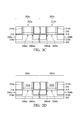
- FIGS. 3A to 3I are cross-sectional representations of various stages of forming a semiconductor structure 200 in accordance with some embodiments. Some materials and processes used to form the semiconductor structure 200 may be similar to, or the same as, those used to form the semiconductor structure 100 and are not repeated herein.
- a substrate 202 includes a first region 201 a and a second region 201 b in accordance with some embodiments.
- the first region 201 a is a core region
- the second region 201 b is an input/output region.
- Core devices may be formed in the core region to perform the designed functions of the semiconductor structure, and input/output devices may be formed in the input/output region to communicate with external circuits.
- a first fin structure 204 a and a second fin structure 204 b may be formed from the substrate 202 in accordance with some embodiments.
- the first fin structure 204 a is formed over the first region 201 a
- the second fin structure 204 b is formed in the second region 201 b in accordance with some embodiments.
- a first protection layer 208 a is formed over the first region 201 a of the substrate 102
- a second protection layer 208 b is formed over the second region 201 b of the substrate 102 , as shown in FIG. 3A in accordance with some embodiments.
- the first protection layer 208 a and the second protection layer 208 b may be similar to the protection layer 108 described previously and are configured to prevent the substrate 202 and the elements formed over the substrate (e.g. the first fin structure 204 a and the second fin structure 204 b ) from being damaged in subsequent manufacturing processes. That is, the first protection layer 208 a and the second protection layer 208 b may be relatively thick.
- first protection layer 208 a and the second protection layer 208 b are formed over different regions of the substrate 202 , they may be formed by performing a single depositing process in accordance with some embodiments. Since the first protection layer 208 a and the second protection layer 208 b may be formed by the same process, the thickness of the first protection layer 208 a may be substantially equal. In some embodiments, both the thickness of the first protection layer 208 a and the thickness of the second protection layer 208 b are in a range from about 20 ⁇ to about 100 ⁇ . As described previously, the first protection layer 208 a and the second protection layer 208 b should be thick enough to protect the substrate 202 underneath in subsequent manufacturing processes. The materials used to form the first protection layer 208 a and the second protection layer 208 b may be similar to those used to form the protection layer 108 and are not repeated herein.
- first protection layer 208 a and the second protection layer 208 b are formed, a first dummy gate structure 212 a and a second dummy gate structure 212 b are formed over the first protection layer 208 a and the second protection layer 208 b respectively, as shown in FIG. 3A in accordance with some embodiments.
- the first protection layer 208 a and the second protection layer 208 b may be configured to protect the first fin structure 204 a and the second fin structure 204 b during the etching process for forming the first dummy gate structure 212 a and the second dummy gate structure 212 b.
- first spacers 214 a and second spacers 214 b are formed on the sidewalls of the first dummy gate structure 212 a and the second dummy gate structure 212 b respectively, as shown in FIG. 3B in accordance with some embodiments.
- the portions of the first protection layer 208 a and the second protection layer 208 b not covered by the first dummy gate structure 212 a , the first spacers 214 a , the second dummy gate structure 212 b , or the second spacers 214 b are removed, as shown in FIG. 3B in accordance with some embodiments.
- the first dummy gate structure 212 a is formed over a first portion 208 ai of the first protection layer 208 a , and the first spacers 214 a are formed over second portions 208 aii of the first protection layer 208 a .
- the second dummy gate structure 212 b is formed over a second portion 208 bi of the second protection layer 208 b , and the second spacers 214 b are formed over second portions 208 bii of the second protection layer 208 b in accordance with some embodiments.
- first source/drain regions 216 a are formed in the first region 201 a of the substrate 102 and at opposite sides of the first dummy gate structure 212 a
- second source/drain regions 216 b are formed in the second region 201 b of the substrate 102 and at opposite sides of the second dummy gate structure 212 b , as shown in FIG. 3B in accordance with some embodiments.
- a contact etch stop layer (CESL) 218 is conformally formed over the substrate 202 , and an interlayer dielectric layer 220 is formed over the contact etch stop layer 218 and the top portion of the contact etch stop layer 218 and the interlayer dielectric layer 220 are polished until the top surfaces of the first dummy gate structure 212 a and the second dummy gate structure 212 b are exposed, as shown in FIG. 3C in accordance with some embodiments.
- the first dummy gate structure 212 a and the second dummy gate structure 212 b are removed to form a first trench 222 a and a second trench 222 b , as shown in FIG. 3D in accordance with some embodiments.
- the first portion 208 ai of the first protection layer 208 a is exposed by the first trench 222 a
- the first portion 208 bi of the second protection layer 208 b is exposed by the second trench 222 b.
- the first portion 208 ai of the first protection layer 208 a and the first portion 208 bi of the second protection layer 208 b are removed, as shown in FIG. 3E in accordance with some embodiments.
- a top surface 205 a of the first fin structure 204 a is exposed by the first trench 222 a
- a top surface 205 b of the second fin structure 204 b is exposed by the second trench 222 b in accordance with some embodiments.
- a first gate dielectric layer 226 a is conformally formed over the first region 201 a of the substrate 102
- a second gate dielectric layer 226 b is conformally formed over the second region 201 b of the substrate 102 , as shown in FIG. 3F in accordance with some embodiments.
- the processes and materials used to form the first gate dielectric layer 226 a and the second gate dielectric layer 226 b may be similar to, or the same as, those of the gate dielectric layer 126 described previously and may not repeated herein.
- the first gate dielectric layer 226 a and the second gate dielectric layer 226 b are formed by performing a single deposition process. Since the first gate dielectric layer 226 a and the second gate dielectric layer 226 b may be formed by performing the same process, the first gate dielectric layer 226 a and the second gate dielectric layer 226 b may be made of the same material and may have a substantially equal thickness. In addition, the first gate dielectric layer 226 a is thinner than the second portion 208 aii of the first protection layer, and the second gate dielectric layer 226 b is thinner than the second portion 208 bii of the second protection layer in accordance with some embodiments.
- a resist layer 223 is formed over the second region 201 b of the substrate 102 to cover the second gate dielectric layer 226 b , as shown in FIG. 3G in accordance with some embodiments.
- the resist layer 223 may be a photoresist layer formed over the second gate dielectric layer 226 b and filled in the second trench 222 b to protect the structure formed in the second region 201 b of the substrate 102 during subsequent manufacturing processes.
- the first gate dielectric layer 226 a is removed, as shown in FIG. 3G in accordance with some embodiments.
- a first metal gate structure 224 a is formed in the first trench 222 a , as shown in FIG. 3H in accordance with some embodiments.
- the first metal gate structure 224 a includes an interfacial layer 225 , a first work function metal layer 228 a , and a first gate electrode layer 230 a.
- the interfacial layer 225 is an oxide layer formed by reacting the top surface 205 a of the first fin structure 204 a with an acidic solution. In some embodiments, the interfacial layer 225 is thinner than the first gate dielectric layer 226 a (i.e. thinner than the second gate dielectric layer 226 b ), so that the resulting first gate structure 224 a can have a lower resistance. Therefore, the operation speed of the first gate structure 224 a can be improved further.
- the processes and materials used to form the first work function metal layer 228 a and the first gate electrode layer 230 a may be similar to, or the same as, those used to form the work function metal layer 128 and the gate electrode layer 130 and are not repeated herein.
- the resist layer 223 is removed, and a second metal gate structure 224 b is formed in the second trench 222 b , as shown in FIG. 3I in accordance with some embodiments.
- the second metal gate structure 224 b includes the second gate dielectric layer 226 b formed previously, a second work function metal layer 228 b , and a second gate electrode layer 230 b .
- the processes and materials used to form the second work function metal layer 228 b and the second gate electrode layer 230 b may be similar to, or the same as, those used to form the work function metal layer 128 and the gate electrode layer 130 and are not repeated herein.
- the first protection layer 208 a and the second protection layer 208 b are formed over the first region 201 a and the second region 201 b of the substrate 102 to prevent the structures underneath from being damaged during subsequent manufacturing processes (e.g. the etching process which is used to form the first dummy gate structure 212 a and the second dummy gate structure 212 b ). Accordingly, the second portion 208 aii of the first protection layer 208 a and the second portion 208 bii of the second protection layer 208 b remaining under the first spacers 214 a and the second spacers 214 b are relatively thick so that they can provide sufficient protection during the manufacturing processes.
- the first protection layer 208 a and the second protection layer 208 b are relatively thick, they may result in high resistance when used in a gate structure. Therefore, in the first metal gate structure 224 a and the second gate structure 224 b , the interfacial layer 225 and the second gate dielectric layer 226 b are formed to replace the first portion 208 ai of the first protection layer 208 a and the second portion 208 bi of the second protection layer 208 b respectively.
- the second portion 208 aii of the first protection layer is thicker than the interfacial layer 225 , such that the interface between the second portion 208 aii of the first protection layer is at a higher position than the top surface of the interfacial layer 225 (e.g. the bottom surface of the work function metal layer 228 a ).
- the semiconductor structure 200 can have less substrate damage due to the formation of the first protection layer 208 a while having a relatively low resistance due to the formation of the interfacial layer 225 . As shown in FIG.
- the interfacial layer 225 is in direct contact with the second portion 208 aii of the first protection layer but is not in direct contact with the first spacers 214 a since the interfacial layer 225 is thinner than the second portion 208 aii of the first protection layer in accordance with some embodiments.
- the sidewall of the first work function metal layer 228 a is in direct contact with both the second portion 208 aii of the first protection layer and the first spacers 214 a in accordance with some embodiments.
- the second portion 208 bii of the second protection layer is thicker than the second gate dielectric layer 226 b , such that the interface between the second portion 208 bii of the second protection layer is at a higher position than the bottom surface of the second work function metal layer 228 b .
- the semiconductor structure 200 can have less substrate damage due to the formation of the second protection layer 208 b while having a relatively low resistance due to the formation of the second gate dielectric layer 226 b .
- the second gate dielectric layer 226 b is in direct contact with both the second portion 208 bii of the second protection layer and the second spacers 214 b in accordance with some embodiments.
- the sidewall of the second work function metal layer 228 b is not in direct contact with neither the second portion 208 bii of the second protection layer nor the second spacers 214 b in accordance with some embodiments.
- the first region 201 a is a core region and the second region 201 b is an input/output region in the semiconductor structure 200 . That is, the first gate structure 224 a formed in the first region 201 a may be used in a core device with a relatively high operating speed and greater current control.
- the first protection layer 208 a is formed over the first region 201 a before the first dummy gate structure 212 a is formed, so that damage to the structure underneath can be prevented and therefore the performance of the resulting semiconductor structure 200 can be improved.
- the first portion 208 ai of the first protection layer 208 a is replaced by the thin interfacial layer 225 in the first gate structure 224 a , and therefore resistance can be decreased and the operation speed can be improved.
- the second gate structure 224 b formed in the second region 201 b may be used in an input/output device to communicate with external circuits. Therefore, the first portion 208 bi of the second protection layer 208 b is replaced by the second gate dielectric layer 226 b in the second gate structure 224 b , so that the second gate dielectric layer 226 b can be thin enough to have a relatively low resistance but still be thick enough to sustain the high voltage applied to the peripheral circuit. In addition, damage to the structure underneath the second protection layer 208 b can also be prevented, and therefore the performance of the semiconductor structure 200 may be improved further.
- the difference between the thickness of the first protection layer 208 a and that of the interfacial layer 225 is in a range from about 5 ⁇ to about 80 ⁇ . In some embodiments, the difference between the thickness of the second protection layer 208 b and that of the second gate dielectric layer 226 b is in a range from about 5 ⁇ to about 70 ⁇ . In some embodiments, the difference between the thickness of the first protection layer 208 a and that of the interfacial layer 225 is greater than the difference between the thickness of the second protection layer 208 b and that of the second gate dielectric layer 226 b . Accordingly, the performance of the first gate structure 224 a used in a core device and that of the second gate structure 224 b used in an input/output device may both be improved.
- Embodiments of methods for forming a semiconductor structure are provided.
- the method may include forming a relatively thick protection layer over a substrate, and a dummy gate structure is formed over the protection layer. Since the protection layer is formed before the dummy gate structure is formed, the substrate can be protected during the processes for forming the dummy gate structure.
- the portion of the protection layer located under the dummy gate structure may be replaced by a gate dielectric layer when the dummy gate structure is replaced by a metal gate structure.
- the gate dielectric layer may be thinner than the protection layer, so the resulting gate structure may have a lower resistance. Accordingly, the resulting semiconductor structure can have a relatively thin gate structure while the damage to the substrate in the semiconductor structure can be prevented by forming the protection layer.
- a method for forming a semiconductor structure includes forming a protection layer having a first portion and a second portion over a substrate and forming a dummy gate structure over the first portion of the protection layer and forming a spacer on a sidewall of the dummy gate structure over a second portion of the protection layer.
- the method for forming a semiconductor structure further includes replacing the first portion of the protection layer and the dummy gate structure by a gate dielectric layer and a gate electrode layer.
- a thickness of the protection layer is greater than a thickness of the gate dielectric layer.
- a method for forming a semiconductor structure includes forming a first protection layer over a first region of a substrate and a second protection layer over a second region of the substrate and forming a first dummy gate structure over the first protection layer and a second dummy gate structure over the second protection layer.
- the method for forming a semiconductor structure further includes forming first spacers over sidewalls of the first dummy gate structure and second spacers over sidewalls of the second dummy gate structure and removing the first dummy gate structure to form a first trench and removing the second dummy gate structure to form a second trench.
- the method for forming a semiconductor structure further includes removing the first protection layer exposed by the first trench and the second protection layer exposed by the second trench and forming a first gate dielectric layer in the first trench and a second gate dielectric layer in the second trench.
- the method for forming a semiconductor structure further includes removing the first gate dielectric layer to expose a portion of a top surface of the substrate and forming an interfacial layer over the portion of the top surface of the substrate exposed by the first trench.
- the method for forming a semiconductor structure further includes forming a first gate structure over the interfacial layer and forming a second gate structure over the second gate dielectric layer.
- a semiconductor structure in some embodiments, includes a first gate structure formed over a first region of a substrate.
- the first gate structure includes an interfacial layer and a first gate electrode layer.
- the semiconductor structure further includes a first protection layer formed adjacent to the first gate structure and a first spacer formed over the first protection layer, such that a sidewall of the first gate structure is covered by the first protection layer and the first spacer.
- an interface between the first protection layer and the first spacer is at a higher position than a top surface of the interfacial layer.
Landscapes
- Metal-Oxide And Bipolar Metal-Oxide Semiconductor Integrated Circuits (AREA)
- Thin Film Transistor (AREA)
- Semiconductor Integrated Circuits (AREA)
Abstract
The method for forming a semiconductor structure includes forming a protection layer having a first portion and a second portion over a substrate and forming a dummy gate layer over the first portion and the second portion of the protection layer. The method for forming a semiconductor structure further includes patterning the dummy gate layer to form a dummy gate structure over the first portion of the protection layer and forming a spacer on a sidewall of the dummy gate structure over a second portion of the protection layer. The method for forming a semiconductor structure further includes replacing the first portion of the protection layer and the dummy gate structure by a gate dielectric layer and a gate electrode layer. In addition, a thickness of the protection layer is greater than a thickness of the gate dielectric layer.
Description
This Application claims the benefit of U.S. Provisional Application No. 62/434,134, filed on Dec. 14, 2016, and entitled “Semiconductor structure with protection layer and method for forming the same”, the entirety of which is incorporated by reference herein.
Semiconductor devices are used in a variety of electronic applications, such as personal computers, cell phones, digital cameras, and other electronic equipment. Semiconductor devices are typically fabricated by sequentially depositing insulating or dielectric layers, conductive layers, and semiconductor layers of material over a semiconductor substrate, and patterning the various material layers using lithography to form circuit components and elements thereon.
Semiconductor devices may include core devices and input/output devices. The core devices may be used to perform the functions of a chip, and the input/output devices may be used to communicate with external circuits in other chips. Although existing manufacturing processes for these semiconductor devices have generally been adequate for their intended purposes, as device scaling-down continues, they have not been entirely satisfactory in all respects.
Aspects of the present disclosure are best understood from the following detailed description when read with the accompanying figures. It should be noted that, in accordance with standard practice in the industry, various features are not drawn to scale. In fact, the dimensions of the various features may be arbitrarily increased or reduced for clarity of discussion.
The following disclosure provides many different embodiments, or examples, for implementing different features of the subject matter provided. Specific examples of components and arrangements are described below to simplify the present disclosure. These are, of course, merely examples and are not intended to be limiting. For example, the formation of a first feature over or on a second feature in the description that follows may include embodiments in which the first and second features are formed in direct contact, and may also include embodiments in which additional features may be formed between the first and second features, such that the first and second features may not be in direct contact. In addition, the present disclosure may repeat reference numerals and/or letters in the various examples. This repetition is for the purpose of simplicity and clarity and does not in itself dictate a relationship between the various embodiments and/or configurations discussed.
Furthermore, spatially relative terms, such as “beneath,” “below,” “lower,” “above,” “upper” and the like, may be used herein for ease of description to describe one element or feature's relationship to another element(s) or feature(s) as illustrated in the figures. The spatially relative terms are intended to encompass different orientations of the device in use or operation in addition to the orientation depicted in the figures. The apparatus may be otherwise oriented (rotated 90 degrees or at other orientations) and the spatially relative descriptors used herein may likewise be interpreted accordingly. It should be understood that additional operations can be provided before, during, and after the method, and some of the operations described can be replaced or eliminated for other embodiments of the method.
Embodiments of semiconductor structures and methods for forming the same are provided. The method for forming the semiconductor structure may include forming a protection layer over a substrate before a dummy gate layer is formed, so that the protection layer may protect the substrate during the process of patterning the dummy gate layer. In addition, the protection layer may be relatively thick to provide better protection for the substrate and may be removed afterwards, so that the performance of the resulting semiconductor structure may be improved.
A fin structure 104 is formed from the substrate 102, and an isolation structure 106 is formed around the fin structure 104, as shown in FIG. 1A in accordance with some embodiments. The fin structure 104 may be formed by patterning the substrate 102. The isolation structure 106 may be formed by forming an insulating material over the substrate 102 and the fin structure 104 and recessing the insulating material to expose the top portion of the fin structure 104. In some embodiments, the insulating material is made of silicon oxide, silicon nitride, silicon oxynitride, fluoride-doped silicate glass (FSG), or other low-K dielectric materials. The insulating material may be formed by using a high-density-plasma (HDP) CVD process, although other deposition processes may be used in other embodiments.
Next, a protection layer 108 is formed over the fin structure 104 and the isolation structure 106, as shown in FIG. 1B in accordance with some embodiments. As shown in FIG. 1B , the protection layer 108 is formed over the top surface of the sidewalls of the fin structure 104 and extends over the top surface of the isolation structure 106. The protection layer 108 may be configured to prevent the substrate 102 and the elements formed over the substrate (e.g. the fin structure 104 and the isolation structure 106) from being damaged in subsequent manufacturing processes, and therefore the protection layer 108 may be relatively thick to protect the elements below it.
In some embodiments, the protection layer 108 has a thickness in a range from about 20 Å to about 100 Å. The protection layer 108 should be thick enough to protect the structure formed below it, while not being too thick or it may be too difficult to be completely removed and therefore undermine the performance of the resulting semiconductor structure.
In some embodiments, the protection layer 108 is an oxide layer. In some embodiments, the protection layer 108 is a silicon oxide layer. In some embodiments, the protection layer 108 is made of metal oxides, metal nitrides, metal silicates, transition metal-oxides, transition metal-nitrides, transition metal-silicates, or oxynitrides of metals. Examples of materials used to form the protection layer 108 include, but are not limited to, hafnium oxide (HfO2), hafnium silicon oxide (HfSiO), hafnium silicon oxynitride (HfSiON), hafnium tantalum oxide (HfTaO), hafnium titanium oxide (HfTiO), hafnium zirconium oxide (HfZrO), silicon nitride, silicon oxynitride, zirconium oxide, titanium oxide, aluminum oxide, hafnium dioxide-alumina (HfO2—Al2O3) alloy, or other applicable dielectric materials.
After the protection layer 108 is formed, a dummy gate layer 110 is formed over the protection layer 108, as shown in FIG. 1C in accordance with some embodiments. In some embodiments, the dummy gate layer 110 is a polysilicon layer.
Next, the dummy gate layer 110 is patterned to form a dummy gate structure 112, as shown in FIG. 1D in accordance with some embodiments. The dummy gate layer 110 may be patterned by forming a mask over a portion of the dummy gate layer 110 and etching the portions of the dummy gate layer 110 not covered by the mask. The dummy gate layer 110 may be etched by performing a dry etching process. The dry etching process may be designed to be stopped when the protection layer 108 is exposed. In addition, as described previously, the protection layer 108 is relatively thick, so that even if some top portions of the protection layer 108 are removed during the etching process, the structure formed underneath (e.g. the fin structure 104 and/or the isolation structure 106) can still be well protected and therefore will not be damaged.
After the dummy gate layer 110 is patterned to form the dummy gate structure 112 over the protection layer 108, spacers 114 are formed on the sidewalls of the dummy gate structure 112, as shown in FIG. 1E in accordance with some embodiments. In addition, the spacers 114 also cover portions of the protection layer 108.
As shown in FIG. 1E , the protection layer 108 includes a first portion 108 i, second portions 108 ii, and third portions 108 iii, and the dummy gate structure 112 is located over a first portion 108 i of the protection layer 108 and the spacers 114 are formed over the second portions 108 ii of the protection layer 108. In addition, the second portions 108 ii of the protection layer 108 are located at the opposite sides of the first portion 108 i of the protection layer 108, and the third portions 108 iii are further apart from the first portion 108 i of the protection layer 108.
In some embodiments, the spacers 114 are made of silicon nitride, silicon oxide, silicon oxynitride, silicon carbide, or other applicable dielectric materials. In some embodiments, the spacers 114 and the protection layer 108 are made of different materials so that they may have relatively good etching selectivity in subsequent etching processes.
After the spacers 114 are formed, the exposed portions of the protection layer 108 are removed, as shown in FIG. 1F in accordance with some embodiments. That is, the third portions 108 iii of the protection layer 108 not covered by the dummy gate structure 112 and the spacers 114 are removed. In some embodiments, the third portions 108 iii of the protection layer 108 are removed by performing an etching process.
Afterwards, source/drain structures 116 are formed in the fin structure 104 adjacent to the dummy gate structure 112, as shown in FIG. 1F in accordance with some embodiments. In addition, the source/drain structures 116 are formed at opposite sides of the dummy gate structure 112 in accordance with some embodiments. The source/drain structures 116 may be formed by recessing the fin structure 104 and growing semiconductor materials in the recesses by performing epitaxial (epi) processes. In some embodiments, the source/drain structures 116 include Ge, SiGe, InAs, InGaAs, InSb, GaAs, GaSb, InAlP, InP, or a combination thereof.
After the source/drain structures 116 are formed, a contact etch stop layer (CESL) 118 is formed over substrate 102, and an interlayer dielectric layer 120 is formed over the contact etch stop layer 118, as shown in FIG. 1H in accordance with some embodiments. In some embodiments, the contact etch stop layer 118 is made of silicon nitride, silicon oxynitride, and/or other applicable materials. The contact etch stop layer 118 may be formed by performing plasma enhanced CVD, low pressure CVD, ALD, or other applicable processes.
The interlayer dielectric layer 120 may include multilayers made of multiple dielectric materials, such as silicon oxide, silicon nitride, silicon oxynitride, phosphosilicate glass (PSG), borophosphosilicate glass (BPSG), and/or other applicable low-k dielectric materials. The interlayer dielectric layer 236 may be formed by performing chemical vapor deposition (CVD), physical vapor deposition, (PVD), atomic layer deposition (ALD), spin-on coating, or other applicable processes.
Next, the dummy gate structure 112 is removed to form a trench 122 between the spacers 114, as shown in FIG. 1H in accordance with some embodiments. In some embodiments, the dummy gate structure 112 is removed by performing a dry etching process. As shown in FIG. 1H , after the dummy gate structure 112 is removed, the first portion 108 i of the protection layer 108 is exposed by the trench 122 while the second portions 108 ii of the protection layer 108 are covered by the spacers 114.
Next, the first portion 108 i of the protection layer 108 exposed by the trench 122 is removed, as shown in FIG. 1I in accordance with some embodiments. In some embodiments, the first portion 108 i of the protection layer 108 is removed by performing a dry etching process. As shown in FIG. 1I , some portions of the fin structure 104 and the isolation structure 106 are exposed by the trench 122 after the first portion 108 i of the protection layer 108 is removed.
Afterwards, a metal gate structure 124 is formed in the trench 122, as shown in FIG. 1J in accordance with some embodiments. In some embodiments, the metal gate structure 124 in the semiconductor structure 100 includes a gate dielectric layer 126, a work function metal layer 128, and a gate electrode layer 130. Since the first portion 108 i of the protection layer 108 is removed before the metal gate structure 124 is formed, the metal gate structure 124 is formed directly on the fin structure 104 and the isolation structure 106.
In some embodiments, the gate dielectric layer 126 and the protection layer 108 are made of the same material, but the protection layer 108 is thicker than the gate dielectric layer 126. As described previously, the protection layer 108 is formed to protect the structures under it (e.g. the fin structure 104 and the isolation structure 106) during subsequent etching processes. Therefore, the protection layer 108 is designed to be relatively thick. On the other hand, the thickness of the gate dielectric layer 126 is designed to be relatively thin, so that the resulting semiconductor structure 100 may have a lower resistance.
In some embodiments, the difference between the thickness of the protection layer 108 and the thickness of the gate dielectric layer 126 is in a range from about 5 Å to about 80 Å. As described above, the difference of the thicknesses between the protection layer 108 and the gate dielectric layer 126 is adjusted, so that the structure under the protection layer 108 can be well protected in previous manufacturing processes (e.g. the etching process shown in FIG. 1D ) while the resulting semiconductor structure 100 can still have a relatively low resistance.
In some embodiments, the gate dielectric layer 126 is an oxide layer. In some embodiments, the gate dielectric layer 126 is a silicon oxide layer. In some embodiments, the gate dielectric layer 126 is made of metal oxides, metal nitrides, metal silicates, transition metal-oxides, transition metal-nitrides, transition metal-silicates, or oxynitrides of metals. Examples of materials used to form the gate dielectric layer 240 include, but are not limited to, hafnium oxide (HfO2), hafnium silicon oxide (HfSiO), hafnium silicon oxynitride (HfSiON), hafnium tantalum oxide (HfTaO), hafnium titanium oxide (HfTiO), hafnium zirconium oxide (HfZrO), silicon nitride, silicon oxynitride, zirconium oxide, titanium oxide, aluminum oxide, hafnium dioxide-alumina (HfO2—Al2O3) alloy, or other applicable dielectric materials.
In some embodiments, the work function metal layer 128 is formed over the gate dielectric layer 126. The work function metal layer 128 may be tuned to have the proper work function. For example, if a P-type work function metal (P-metal) for a PMOS device is desired, P-type work function materials may be used. Examples of P-type work function materials include, but are not limited to, titanium nitride (TiN), tungsten nitride (WN), tungsten (W), ruthenium (Ru), palladium (Pd), platinum (Pt), cobalt (Co), nickel (Ni), conductive metal oxides, and/or other applicable materials.
On the other hand, if an N-type work function metal (N-metal) for NMOS devices is desired, N-type metal materials may be used. Examples of N-type work function materials include, but are not limited to, titanium aluminide (TiAl), titanium aluminium nitride (TiAlN), carbo-nitride tantalum (TaCN), hafnium (Hf), zirconium (Zr), titanium (Ti), tantalum (Ta), aluminum (Al), metal carbides (e.g., hafnium carbide (HfC), zirconium carbide (ZrC), titanium carbide (TiC), aluminum carbide (AlC), aluminides, and/or other applicable materials.
In some embodiments, the gate electrode layer 130 is formed over the work function metal layer 128. In some embodiments, the gate electrode layer 130 is made of a conductive material, such as aluminum, copper, tungsten, titanium, tantalum, titanium nitride, tantalum nitride, nickel silicide, cobalt silicide, TaC, TaSiN, TaCN, TiAl, TiAlN, or other applicable materials.
As described previously, the protection layer 108 is formed over the fin structure 104 and the isolation structure 106 before the dummy gate layer 110 is formed. Therefore, the protection layer 108 can protect the structure below it from being damaged during the etching process for patterning the dummy gate layer 110. In addition, the first portion 108 i of the protection layer 108 located under the dummy gate structure 112 is replaced by a relatively thin gate dielectric layer 126, and therefore the resulting semiconductor structure 100 can still have a relatively low resistance. Since damage to the fin structure 104 and the isolation structure 106 can be prevented while the semiconductor structure 100 can still have a relatively thin gate dielectric layer 126, the performance of the semiconductor structure 100 can be improved.
It should be noted that, although the first portion 108 i, the second portions 108 ii and the third portions 108 iii of the protection layer 108 are shown in the figures described above, there are no real boundaries (e.g. interfaces) between each portion. That is, these portions are merely shown to provide a better understanding of the concept of the disclosure, but the scope of the disclosure is not intended to be limiting.
As described previously, the gate dielectric layer 126 and the protection layer 108 (i.e. the second portion 108 ii of the protection layer 108) may be made of the same material. In some embodiments, the gate dielectric layer 126 and the second portion 108 ii of the protection layer are made of a same oxide, such that an oxide layer is position between the work function metal layer 128 of the gate structure 124 and the spacer 114 and further extends under the work function metal layer 128 and the spacer 114. In addition, the extending portion of the oxide layer located under the spacer 114 (i.e. the second portion 108 ii of the protection layer 108) is thicker than the extending portion of the oxide layer located under the work function metal layer 128 (i.e. the gate dielectric layer 126).
As shown in FIG. 3A , a substrate 202 includes a first region 201 a and a second region 201 b in accordance with some embodiments. In some embodiments, the first region 201 a is a core region, and the second region 201 b is an input/output region. Core devices may be formed in the core region to perform the designed functions of the semiconductor structure, and input/output devices may be formed in the input/output region to communicate with external circuits.
Similar to the processes described previously related to FIG. 1A , a first fin structure 204 a and a second fin structure 204 b may be formed from the substrate 202 in accordance with some embodiments. In addition, the first fin structure 204 a is formed over the first region 201 a, and the second fin structure 204 b is formed in the second region 201 b in accordance with some embodiments.
Next, a first protection layer 208 a is formed over the first region 201 a of the substrate 102, and a second protection layer 208 b is formed over the second region 201 b of the substrate 102, as shown in FIG. 3A in accordance with some embodiments. The first protection layer 208 a and the second protection layer 208 b may be similar to the protection layer 108 described previously and are configured to prevent the substrate 202 and the elements formed over the substrate (e.g. the first fin structure 204 a and the second fin structure 204 b) from being damaged in subsequent manufacturing processes. That is, the first protection layer 208 a and the second protection layer 208 b may be relatively thick.
In addition, although the first protection layer 208 a and the second protection layer 208 b are formed over different regions of the substrate 202, they may be formed by performing a single depositing process in accordance with some embodiments. Since the first protection layer 208 a and the second protection layer 208 b may be formed by the same process, the thickness of the first protection layer 208 a may be substantially equal. In some embodiments, both the thickness of the first protection layer 208 a and the thickness of the second protection layer 208 b are in a range from about 20 Å to about 100 Å. As described previously, the first protection layer 208 a and the second protection layer 208 b should be thick enough to protect the substrate 202 underneath in subsequent manufacturing processes. The materials used to form the first protection layer 208 a and the second protection layer 208 b may be similar to those used to form the protection layer 108 and are not repeated herein.
After the first protection layer 208 a and the second protection layer 208 b are formed, a first dummy gate structure 212 a and a second dummy gate structure 212 b are formed over the first protection layer 208 a and the second protection layer 208 b respectively, as shown in FIG. 3A in accordance with some embodiments. As described previously, the first protection layer 208 a and the second protection layer 208 b may be configured to protect the first fin structure 204 a and the second fin structure 204 b during the etching process for forming the first dummy gate structure 212 a and the second dummy gate structure 212 b.
Next, first spacers 214 a and second spacers 214 b are formed on the sidewalls of the first dummy gate structure 212 a and the second dummy gate structure 212 b respectively, as shown in FIG. 3B in accordance with some embodiments. Afterwards, the portions of the first protection layer 208 a and the second protection layer 208 b not covered by the first dummy gate structure 212 a, the first spacers 214 a, the second dummy gate structure 212 b, or the second spacers 214 b are removed, as shown in FIG. 3B in accordance with some embodiments. In some embodiments, the first dummy gate structure 212 a is formed over a first portion 208 ai of the first protection layer 208 a, and the first spacers 214 a are formed over second portions 208 aii of the first protection layer 208 a. Similarly, the second dummy gate structure 212 b is formed over a second portion 208 bi of the second protection layer 208 b, and the second spacers 214 b are formed over second portions 208 bii of the second protection layer 208 b in accordance with some embodiments.
Afterwards, first source/drain regions 216 a are formed in the first region 201 a of the substrate 102 and at opposite sides of the first dummy gate structure 212 a, and second source/drain regions 216 b are formed in the second region 201 b of the substrate 102 and at opposite sides of the second dummy gate structure 212 b, as shown in FIG. 3B in accordance with some embodiments. After the first source/drain regions 216 a and the second source/drain regions 216 b are formed, a contact etch stop layer (CESL) 218 is conformally formed over the substrate 202, and an interlayer dielectric layer 220 is formed over the contact etch stop layer 218 and the top portion of the contact etch stop layer 218 and the interlayer dielectric layer 220 are polished until the top surfaces of the first dummy gate structure 212 a and the second dummy gate structure 212 b are exposed, as shown in FIG. 3C in accordance with some embodiments.
Next, the first dummy gate structure 212 a and the second dummy gate structure 212 b are removed to form a first trench 222 a and a second trench 222 b, as shown in FIG. 3D in accordance with some embodiments. As shown in FIG. 3D , after the first dummy gate structure 212 a and the second dummy gate structure 212 b are removed, the first portion 208 ai of the first protection layer 208 a is exposed by the first trench 222 a, and the first portion 208 bi of the second protection layer 208 b is exposed by the second trench 222 b.
After the first dummy gate structure 212 a and the second dummy gate structure 212 b are removed, the first portion 208 ai of the first protection layer 208 a and the first portion 208 bi of the second protection layer 208 b are removed, as shown in FIG. 3E in accordance with some embodiments. As shown in FIG. 3E , a top surface 205 a of the first fin structure 204 a is exposed by the first trench 222 a, and a top surface 205 b of the second fin structure 204 b is exposed by the second trench 222 b in accordance with some embodiments.
Afterwards, a first gate dielectric layer 226 a is conformally formed over the first region 201 a of the substrate 102, and a second gate dielectric layer 226 b is conformally formed over the second region 201 b of the substrate 102, as shown in FIG. 3F in accordance with some embodiments. The processes and materials used to form the first gate dielectric layer 226 a and the second gate dielectric layer 226 b may be similar to, or the same as, those of the gate dielectric layer 126 described previously and may not repeated herein.
In some embodiments, the first gate dielectric layer 226 a and the second gate dielectric layer 226 b are formed by performing a single deposition process. Since the first gate dielectric layer 226 a and the second gate dielectric layer 226 b may be formed by performing the same process, the first gate dielectric layer 226 a and the second gate dielectric layer 226 b may be made of the same material and may have a substantially equal thickness. In addition, the first gate dielectric layer 226 a is thinner than the second portion 208 aii of the first protection layer, and the second gate dielectric layer 226 b is thinner than the second portion 208 bii of the second protection layer in accordance with some embodiments.
Next, a resist layer 223 is formed over the second region 201 b of the substrate 102 to cover the second gate dielectric layer 226 b, as shown in FIG. 3G in accordance with some embodiments. The resist layer 223 may be a photoresist layer formed over the second gate dielectric layer 226 b and filled in the second trench 222 b to protect the structure formed in the second region 201 b of the substrate 102 during subsequent manufacturing processes. After the resist layer 223 is formed, the first gate dielectric layer 226 a is removed, as shown in FIG. 3G in accordance with some embodiments.
After the first gate dielectric layer 226 a is removed, a first metal gate structure 224 a is formed in the first trench 222 a, as shown in FIG. 3H in accordance with some embodiments. In some embodiments, the first metal gate structure 224 a includes an interfacial layer 225, a first work function metal layer 228 a, and a first gate electrode layer 230 a.
In some embodiments, the interfacial layer 225 is an oxide layer formed by reacting the top surface 205 a of the first fin structure 204 a with an acidic solution. In some embodiments, the interfacial layer 225 is thinner than the first gate dielectric layer 226 a (i.e. thinner than the second gate dielectric layer 226 b), so that the resulting first gate structure 224 a can have a lower resistance. Therefore, the operation speed of the first gate structure 224 a can be improved further. The processes and materials used to form the first work function metal layer 228 a and the first gate electrode layer 230 a may be similar to, or the same as, those used to form the work function metal layer 128 and the gate electrode layer 130 and are not repeated herein.
After the first metal gate structure 224 a is formed, the resist layer 223 is removed, and a second metal gate structure 224 b is formed in the second trench 222 b, as shown in FIG. 3I in accordance with some embodiments. In some embodiments, the second metal gate structure 224 b includes the second gate dielectric layer 226 b formed previously, a second work function metal layer 228 b, and a second gate electrode layer 230 b. The processes and materials used to form the second work function metal layer 228 b and the second gate electrode layer 230 b may be similar to, or the same as, those used to form the work function metal layer 128 and the gate electrode layer 130 and are not repeated herein.
As described previously, the first protection layer 208 a and the second protection layer 208 b are formed over the first region 201 a and the second region 201 b of the substrate 102 to prevent the structures underneath from being damaged during subsequent manufacturing processes (e.g. the etching process which is used to form the first dummy gate structure 212 a and the second dummy gate structure 212 b). Accordingly, the second portion 208 aii of the first protection layer 208 a and the second portion 208 bii of the second protection layer 208 b remaining under the first spacers 214 a and the second spacers 214 b are relatively thick so that they can provide sufficient protection during the manufacturing processes.
However, since the first protection layer 208 a and the second protection layer 208 b are relatively thick, they may result in high resistance when used in a gate structure. Therefore, in the first metal gate structure 224 a and the second gate structure 224 b, the interfacial layer 225 and the second gate dielectric layer 226 b are formed to replace the first portion 208 ai of the first protection layer 208 a and the second portion 208 bi of the second protection layer 208 b respectively.
In some embodiments, the second portion 208 aii of the first protection layer is thicker than the interfacial layer 225, such that the interface between the second portion 208 aii of the first protection layer is at a higher position than the top surface of the interfacial layer 225 (e.g. the bottom surface of the work function metal layer 228 a). As described previously, the semiconductor structure 200 can have less substrate damage due to the formation of the first protection layer 208 a while having a relatively low resistance due to the formation of the interfacial layer 225. As shown in FIG. 3I , the interfacial layer 225 is in direct contact with the second portion 208 aii of the first protection layer but is not in direct contact with the first spacers 214 a since the interfacial layer 225 is thinner than the second portion 208 aii of the first protection layer in accordance with some embodiments. On the other hand, the sidewall of the first work function metal layer 228 a is in direct contact with both the second portion 208 aii of the first protection layer and the first spacers 214 a in accordance with some embodiments.
In some embodiments, the second portion 208 bii of the second protection layer is thicker than the second gate dielectric layer 226 b, such that the interface between the second portion 208 bii of the second protection layer is at a higher position than the bottom surface of the second work function metal layer 228 b. Similarly, the semiconductor structure 200 can have less substrate damage due to the formation of the second protection layer 208 b while having a relatively low resistance due to the formation of the second gate dielectric layer 226 b. As shown in FIG. 3I , the second gate dielectric layer 226 b is in direct contact with both the second portion 208 bii of the second protection layer and the second spacers 214 b in accordance with some embodiments. On the other hand, the sidewall of the second work function metal layer 228 b is not in direct contact with neither the second portion 208 bii of the second protection layer nor the second spacers 214 b in accordance with some embodiments.
Furthermore, in some embodiments, the first region 201 a is a core region and the second region 201 b is an input/output region in the semiconductor structure 200. That is, the first gate structure 224 a formed in the first region 201 a may be used in a core device with a relatively high operating speed and greater current control. As described previously, the first protection layer 208 a is formed over the first region 201 a before the first dummy gate structure 212 a is formed, so that damage to the structure underneath can be prevented and therefore the performance of the resulting semiconductor structure 200 can be improved. In addition, the first portion 208 ai of the first protection layer 208 a is replaced by the thin interfacial layer 225 in the first gate structure 224 a, and therefore resistance can be decreased and the operation speed can be improved.
On the other hand, the second gate structure 224 b formed in the second region 201 b may be used in an input/output device to communicate with external circuits. Therefore, the first portion 208 bi of the second protection layer 208 b is replaced by the second gate dielectric layer 226 b in the second gate structure 224 b, so that the second gate dielectric layer 226 b can be thin enough to have a relatively low resistance but still be thick enough to sustain the high voltage applied to the peripheral circuit. In addition, damage to the structure underneath the second protection layer 208 b can also be prevented, and therefore the performance of the semiconductor structure 200 may be improved further.
In some embodiments, the difference between the thickness of the first protection layer 208 a and that of the interfacial layer 225 is in a range from about 5 Å to about 80 Å. In some embodiments, the difference between the thickness of the second protection layer 208 b and that of the second gate dielectric layer 226 b is in a range from about 5 Å to about 70 Å. In some embodiments, the difference between the thickness of the first protection layer 208 a and that of the interfacial layer 225 is greater than the difference between the thickness of the second protection layer 208 b and that of the second gate dielectric layer 226 b. Accordingly, the performance of the first gate structure 224 a used in a core device and that of the second gate structure 224 b used in an input/output device may both be improved.
Embodiments of methods for forming a semiconductor structure are provided. The method may include forming a relatively thick protection layer over a substrate, and a dummy gate structure is formed over the protection layer. Since the protection layer is formed before the dummy gate structure is formed, the substrate can be protected during the processes for forming the dummy gate structure. In addition, the portion of the protection layer located under the dummy gate structure may be replaced by a gate dielectric layer when the dummy gate structure is replaced by a metal gate structure. The gate dielectric layer may be thinner than the protection layer, so the resulting gate structure may have a lower resistance. Accordingly, the resulting semiconductor structure can have a relatively thin gate structure while the damage to the substrate in the semiconductor structure can be prevented by forming the protection layer.
In some embodiments, a method for forming a semiconductor structure is provided. The method for forming a semiconductor structure includes forming a protection layer having a first portion and a second portion over a substrate and forming a dummy gate structure over the first portion of the protection layer and forming a spacer on a sidewall of the dummy gate structure over a second portion of the protection layer. The method for forming a semiconductor structure further includes replacing the first portion of the protection layer and the dummy gate structure by a gate dielectric layer and a gate electrode layer. In addition, a thickness of the protection layer is greater than a thickness of the gate dielectric layer.
In some embodiments, a method for forming a semiconductor structure is provided. The method for forming a semiconductor structure includes forming a first protection layer over a first region of a substrate and a second protection layer over a second region of the substrate and forming a first dummy gate structure over the first protection layer and a second dummy gate structure over the second protection layer. The method for forming a semiconductor structure further includes forming first spacers over sidewalls of the first dummy gate structure and second spacers over sidewalls of the second dummy gate structure and removing the first dummy gate structure to form a first trench and removing the second dummy gate structure to form a second trench. The method for forming a semiconductor structure further includes removing the first protection layer exposed by the first trench and the second protection layer exposed by the second trench and forming a first gate dielectric layer in the first trench and a second gate dielectric layer in the second trench. The method for forming a semiconductor structure further includes removing the first gate dielectric layer to expose a portion of a top surface of the substrate and forming an interfacial layer over the portion of the top surface of the substrate exposed by the first trench. The method for forming a semiconductor structure further includes forming a first gate structure over the interfacial layer and forming a second gate structure over the second gate dielectric layer.
In some embodiments, a semiconductor structure is provided. The semiconductor structure includes a first gate structure formed over a first region of a substrate. In addition, the first gate structure includes an interfacial layer and a first gate electrode layer. The semiconductor structure further includes a first protection layer formed adjacent to the first gate structure and a first spacer formed over the first protection layer, such that a sidewall of the first gate structure is covered by the first protection layer and the first spacer. In addition, an interface between the first protection layer and the first spacer is at a higher position than a top surface of the interfacial layer.
The foregoing outlines features of several embodiments so that those skilled in the art may better understand the aspects of the present disclosure. Those skilled in the art should appreciate that they may readily use the present disclosure as a basis for designing or modifying other processes and structures for carrying out the same purposes and/or achieving the same advantages of the embodiments introduced herein. Those skilled in the art should also realize that such equivalent constructions do not depart from the spirit and scope of the present disclosure, and that they may make various changes, substitutions, and alterations herein without departing from the spirit and scope of the present disclosure.
Claims (20)
1. A method for forming a semiconductor structure, comprising:
forming a first protection layer having a first portion, a second portion and a third portion over a first portion of a substrate;
forming a first dummy gate structure over the first portion of the first protection layer;
forming a first spacer on a sidewall of the first dummy gate structure and over the second portion of the first protection layer;
removing the third portion of the first protection layer which is exposed by the first dummy gate structure and the first spacer;
replacing the first portion of the first protection layer and the first dummy gate structure by a first gate dielectric layer, wherein a thickness of the first protection layer is greater than a thickness of the first gate dielectric layer;
replacing the first gate dielectric layer by an interfacial layer, wherein the thickness of the first gate dielectric layer is greater than a thickness of the interfacial layer; and
forming a first gate electrode layer over the interfacial layer.
2. The method for forming a semiconductor structure as claimed in claim 1 , wherein the thickness of the first protection layer is in a range from about 20 Å to about 100 Å.
3. The method for forming a semiconductor structure as claimed in claim 2 , wherein a difference between the thickness of the first protection layer and the thickness of the first gate dielectric layer is in a range of about 5 Å to about 80 Å.
4. The method for forming a semiconductor structure as claimed in claim 1 , wherein the first protection layer and the first gate dielectric layer are made of a same material.
5. The method for forming a semiconductor structure as claimed in claim 4 , wherein the second portion of the first protection layer is in direct contact with the first gate dielectric layer.
6. The method for forming a semiconductor structure as claimed in claim 1 , further comprising:
forming a fin structure over the substrate;
forming an isolation structure around the fin structure,
wherein the first protection layer is formed over the fin structure and extends over the isolation structure.
7. The method for forming a semiconductor structure as claimed in claim 1 , further comprising:
forming a second protection layer having a first portion, a second portion and a third portion over a second portion of the substrate;
forming a second dummy gate structure over the first portion of the second protection layer;
forming a second spacer on a sidewall of the second dummy gate structure and over the second portion of the second protection layer;
removing the third portion of the second protection layer which is exposed by the second dummy gate structure and the second spacer; and
replacing the first portion of the second protection layer and the second dummy gate structure by a second gate dielectric layer and a second gate electrode layer, wherein the first gate dielectric layer and the second gate dielectric layer are formed by a single process.
8. A method for forming a semiconductor structure, comprising:
forming a first protection layer over a first region of a substrate and a second protection layer over a second region of the substrate;
forming a first dummy gate structure over the first protection layer and a second dummy gate structure over the second protection layer;
forming first spacers over sidewalls of the first dummy gate structure and second spacers over sidewalls of the second dummy gate structure;
removing the first dummy gate structure to form a first trench and removing the second dummy gate structure to form a second trench;
removing the first protection layer exposed by the first trench and the second protection layer exposed by the second trench;
forming a first gate dielectric layer in the first trench and a second gate dielectric layer in the second trench, wherein a thickness of the first protection layer is greater than a thickness of the first gate dielectric layer;
removing the first gate dielectric layer to expose a portion of a top surface of the substrate;
forming an interfacial layer over the portion of the top surface of the substrate exposed by the first trench;
forming a first gate structure over the interfacial layer; and
forming a second gate structure over the second gate dielectric layer.
9. The method for forming a semiconductor structure as claimed in claim 8 , wherein the first gate dielectric layer and the second gate dielectric layer are formed by performing a same deposition process.
10. The method for forming a semiconductor structure as claimed in claim 8 , wherein an interface between the first protection layer and the first spacer is at a higher position than a top surface of the interfacial layer.
11. The method for forming a semiconductor structure as claimed in claim 8 , wherein the second protection layer is thicker than the second gate dielectric layer.
12. The method for forming a semiconductor structure as claimed in claim 8 , wherein the first region is a core region and the second region is an input/output region.
13. The method for forming a semiconductor structure as claimed in claim 8 , wherein the first protection layer is thicker than the second gate dielectric layer, and the second gate dielectric layer is thicker than the interfacial layer.
14. The method for forming a semiconductor structure as claimed in claim 8 , wherein the first protection layer, the second protection layer and the second gate dielectric layer are made of a same material.
15. The method for forming a semiconductor structure as claimed in claim 14 , wherein the first protection layer and the second protection layer are formed by performing a same deposition process.
16. A method for forming a semiconductor structure, comprising:
forming a protection layer over a fin structure of a substrate;
forming a dummy gate structure across the fin structure and over the protection layer;
forming a spacer on a sidewall of the dummy gate structure and over the protection layer;
removing the dummy gate structure to form a trench exposing a portion of the protection layer;
removing the portion of the protection layer exposed by the trench, wherein a width of the protection layer is substantially the same as a width of the spacer after removing the portion of the protection layer;
forming a gate dielectric layer in the trench, wherein the protection layer and the gate dielectric layer are made of a same material and a thickness of the protection layer is greater than a thickness of the gate dielectric layer;
removing the gate dielectric layer to expose a portion of a top surface of the fin structure; and
forming an interfacial layer over the portion of the top surface of the fin structure exposed by the trench, wherein the thickness of the protection layer is greater than a thickness of the interfacial layer.
17. The method for forming a semiconductor structure as claimed in claim 16 , wherein the thickness of the protection layer is in a range from about 20 Å to about 100 Å.
18. The method for forming a semiconductor structure as claimed in claim 16 , wherein the protection layer is an oxide layer.
19. The method for forming a semiconductor structure as claimed in claim 16 , wherein the portion of the protection layer is in direct contact with the gate dielectric layer.
20. The method for forming a semiconductor structure as claimed in claim 16 , further comprising:
forming a gate electrode layer over the gate dielectric layer.
Priority Applications (1)
| Application Number | Priority Date | Filing Date | Title |
|---|---|---|---|
| US15/434,343 US10164063B2 (en) | 2016-12-14 | 2017-02-16 | Semiconductor structure with protection layer |
Applications Claiming Priority (2)
| Application Number | Priority Date | Filing Date | Title |
|---|---|---|---|
| US201662434134P | 2016-12-14 | 2016-12-14 | |
| US15/434,343 US10164063B2 (en) | 2016-12-14 | 2017-02-16 | Semiconductor structure with protection layer |
Publications (2)
| Publication Number | Publication Date |
|---|---|
| US20180166560A1 US20180166560A1 (en) | 2018-06-14 |
| US10164063B2 true US10164063B2 (en) | 2018-12-25 |
Family
ID=62489731
Family Applications (1)
| Application Number | Title | Priority Date | Filing Date |
|---|---|---|---|
| US15/434,343 Active US10164063B2 (en) | 2016-12-14 | 2017-02-16 | Semiconductor structure with protection layer |
Country Status (1)
| Country | Link |
|---|---|
| US (1) | US10164063B2 (en) |
Families Citing this family (11)
| Publication number | Priority date | Publication date | Assignee | Title |
|---|---|---|---|---|
| US10020304B2 (en) * | 2015-11-16 | 2018-07-10 | Taiwan Semiconductor Manufacturing Co., Ltd. | Fin field effect transistor, semiconductor device and fabricating method thereof |
| US10651171B2 (en) * | 2016-12-15 | 2020-05-12 | Taiwan Semiconductor Manufacturing Co. Ltd. | Integrated circuit with a gate structure and method making the same |
| US10079290B2 (en) * | 2016-12-30 | 2018-09-18 | United Microelectronics Corp. | Semiconductor device having asymmetric spacer structures |
| US10062784B1 (en) | 2017-04-20 | 2018-08-28 | Taiwan Semiconductor Manufacturing Company, Ltd. | Self-aligned gate hard mask and method forming same |
| US10236220B1 (en) * | 2017-08-31 | 2019-03-19 | Taiwan Semiconductor Manufacturing Company, Ltd. | Fin field-effect transistor device and method |
| CN111029302A (en) * | 2018-10-09 | 2020-04-17 | 中芯国际集成电路制造(上海)有限公司 | Semiconductor device and method of forming the same |
| US11211472B2 (en) * | 2020-02-24 | 2021-12-28 | Taiwan Semiconductor Manufacturing Co., Ltd. | Semiconductor device and method of forming the same |
| US11742404B2 (en) * | 2020-04-29 | 2023-08-29 | Taiwan Semiconductor Manufacturing Co., Ltd. | Method of manufacturing a semiconductor device and a semiconductor device |
| CN113764504B (en) * | 2020-06-03 | 2025-05-02 | 中芯北方集成电路制造(北京)有限公司 | Semiconductor structure and method for forming the same |
| KR102780362B1 (en) * | 2020-10-23 | 2025-03-17 | 삼성전자주식회사 | Semiconductor device |
| US20230008994A1 (en) * | 2021-07-09 | 2023-01-12 | Taiwan Semiconductor Manufacturing Co., Ltd. | Semiconductor device with dielectric layer and method of forming the same |
Citations (9)
| Publication number | Priority date | Publication date | Assignee | Title |
|---|---|---|---|---|
| US8487378B2 (en) | 2011-01-21 | 2013-07-16 | Taiwan Semiconductor Manufacturing Company, Ltd. | Non-uniform channel junction-less transistor |
| US20140001540A1 (en) * | 2012-07-02 | 2014-01-02 | Semiconductor Manufacturing International Corp. | Integrated semiconductor device and fabrication method |
| US20140070285A1 (en) * | 2012-09-12 | 2014-03-13 | International Business Machines Corporation | Methods of forming semiconductor devices with self-aligned contacts and the resulting devices |
| US8729634B2 (en) | 2012-06-15 | 2014-05-20 | Taiwan Semiconductor Manufacturing Company, Ltd. | FinFET with high mobility and strain channel |
| US8826213B1 (en) | 2013-03-11 | 2014-09-02 | Taiwan Semiconductor Manufacturing Company, Ltd. | Parasitic capacitance extraction for FinFETs |
| US20140282326A1 (en) | 2013-03-12 | 2014-09-18 | Taiwan Semiconductor Manufacturing Company, Ltd. | Methods for Layout Verification for Polysilicon Cell Edge Structures in FinFET Standard Cells |
| US8887106B2 (en) | 2011-12-28 | 2014-11-11 | Taiwan Semiconductor Manufacturing Company, Ltd. | Method of generating a bias-adjusted layout design of a conductive feature and method of generating a simulation model of a predefined fabrication process |
| US20160064225A1 (en) * | 2014-09-01 | 2016-03-03 | Weon-Hong Kim | Method for fabricating semiconductor device |
| US20160181384A1 (en) * | 2014-12-23 | 2016-06-23 | Stmicroelectronics, Inc. | Reduced trench profile for a gate |
-
2017
- 2017-02-16 US US15/434,343 patent/US10164063B2/en active Active
Patent Citations (9)
| Publication number | Priority date | Publication date | Assignee | Title |
|---|---|---|---|---|
| US8487378B2 (en) | 2011-01-21 | 2013-07-16 | Taiwan Semiconductor Manufacturing Company, Ltd. | Non-uniform channel junction-less transistor |
| US8887106B2 (en) | 2011-12-28 | 2014-11-11 | Taiwan Semiconductor Manufacturing Company, Ltd. | Method of generating a bias-adjusted layout design of a conductive feature and method of generating a simulation model of a predefined fabrication process |
| US8729634B2 (en) | 2012-06-15 | 2014-05-20 | Taiwan Semiconductor Manufacturing Company, Ltd. | FinFET with high mobility and strain channel |
| US20140001540A1 (en) * | 2012-07-02 | 2014-01-02 | Semiconductor Manufacturing International Corp. | Integrated semiconductor device and fabrication method |
| US20140070285A1 (en) * | 2012-09-12 | 2014-03-13 | International Business Machines Corporation | Methods of forming semiconductor devices with self-aligned contacts and the resulting devices |
| US8826213B1 (en) | 2013-03-11 | 2014-09-02 | Taiwan Semiconductor Manufacturing Company, Ltd. | Parasitic capacitance extraction for FinFETs |
| US20140282326A1 (en) | 2013-03-12 | 2014-09-18 | Taiwan Semiconductor Manufacturing Company, Ltd. | Methods for Layout Verification for Polysilicon Cell Edge Structures in FinFET Standard Cells |
| US20160064225A1 (en) * | 2014-09-01 | 2016-03-03 | Weon-Hong Kim | Method for fabricating semiconductor device |
| US20160181384A1 (en) * | 2014-12-23 | 2016-06-23 | Stmicroelectronics, Inc. | Reduced trench profile for a gate |
Also Published As
| Publication number | Publication date |
|---|---|
| US20180166560A1 (en) | 2018-06-14 |
Similar Documents
| Publication | Publication Date | Title |
|---|---|---|
| US10164063B2 (en) | Semiconductor structure with protection layer | |
| US10096693B2 (en) | Method for manufacturing semiconductor structure with multi spacers | |
| US11271089B2 (en) | Method for manufacturing semiconductor structure with unleveled gate structure | |
| US11217683B2 (en) | Semiconductor structure with extending gate structure and method for forming the same | |
| US9922978B2 (en) | Semiconductor structure with recessed source/drain structure and method for forming the same | |
| US12074218B2 (en) | Contact structure with insulating cap | |
| US11081585B2 (en) | Via structure with low resistivity and method for forming the same | |
| US9324820B1 (en) | Method for forming semiconductor structure with metallic layer over source/drain structure | |
| KR20160026663A (en) | Semiconductor structure with contact over source/drain structure and method for forming the same | |
| US12191366B2 (en) | Semiconductor structure with enlarged gate electrode structure and method for forming the same | |
| US10763305B2 (en) | Semiconductor structure with data storage structure | |
| US9391205B2 (en) | Gate last semiconductor structure and method for forming the same | |
| US20240105805A1 (en) | Semiconductor structure with dielectric wall structure and method for manufacturing the same | |
| US20240079447A1 (en) | Semiconductor structure and method for forming the same | |
| US20240079500A1 (en) | Semiconductor structure and method for forming the same | |
| US20240113195A1 (en) | Semiconductor structure and method for forming the same | |
| US20250126858A1 (en) | Semiconductor structure and method for forming the same | |
| US10157781B2 (en) | Method for forming semiconductor structure using polishing process |
Legal Events
| Date | Code | Title | Description |
|---|---|---|---|
| AS | Assignment |
Owner name: TAIWAN SEMICONDUCTOR MANUFACTURING CO., LTD., TAIW Free format text: ASSIGNMENT OF ASSIGNORS INTEREST;ASSIGNORS:CHIANG, CHIH-WEI;LEU, PO-HSIUNG;LIU, DING-I;SIGNING DATES FROM 20170210 TO 20170214;REEL/FRAME:041285/0546 |
|
| STCF | Information on status: patent grant |
Free format text: PATENTED CASE |
|
| MAFP | Maintenance fee payment |
Free format text: PAYMENT OF MAINTENANCE FEE, 4TH YEAR, LARGE ENTITY (ORIGINAL EVENT CODE: M1551); ENTITY STATUS OF PATENT OWNER: LARGE ENTITY Year of fee payment: 4 |