US10146475B2 - Memory device performing control of discarding packet - Google Patents
Memory device performing control of discarding packet Download PDFInfo
- Publication number
- US10146475B2 US10146475B2 US14/580,788 US201414580788A US10146475B2 US 10146475 B2 US10146475 B2 US 10146475B2 US 201414580788 A US201414580788 A US 201414580788A US 10146475 B2 US10146475 B2 US 10146475B2
- Authority
- US
- United States
- Prior art keywords
- packet
- initiator
- header
- interface circuit
- data
- Prior art date
- Legal status (The legal status is an assumption and is not a legal conclusion. Google has not performed a legal analysis and makes no representation as to the accuracy of the status listed.)
- Active, expires
Links
Images


Classifications
-
- G—PHYSICS
- G06—COMPUTING OR CALCULATING; COUNTING
- G06F—ELECTRIC DIGITAL DATA PROCESSING
- G06F3/00—Input arrangements for transferring data to be processed into a form capable of being handled by the computer; Output arrangements for transferring data from processing unit to output unit, e.g. interface arrangements
- G06F3/06—Digital input from, or digital output to, record carriers, e.g. RAID, emulated record carriers or networked record carriers
- G06F3/0601—Interfaces specially adapted for storage systems
- G06F3/0628—Interfaces specially adapted for storage systems making use of a particular technique
- G06F3/0655—Vertical data movement, i.e. input-output transfer; data movement between one or more hosts and one or more storage devices
- G06F3/0659—Command handling arrangements, e.g. command buffers, queues, command scheduling
-
- G—PHYSICS
- G06—COMPUTING OR CALCULATING; COUNTING
- G06F—ELECTRIC DIGITAL DATA PROCESSING
- G06F3/00—Input arrangements for transferring data to be processed into a form capable of being handled by the computer; Output arrangements for transferring data from processing unit to output unit, e.g. interface arrangements
- G06F3/06—Digital input from, or digital output to, record carriers, e.g. RAID, emulated record carriers or networked record carriers
- G06F3/0601—Interfaces specially adapted for storage systems
- G06F3/0602—Interfaces specially adapted for storage systems specifically adapted to achieve a particular effect
- G06F3/061—Improving I/O performance
-
- G—PHYSICS
- G06—COMPUTING OR CALCULATING; COUNTING
- G06F—ELECTRIC DIGITAL DATA PROCESSING
- G06F3/00—Input arrangements for transferring data to be processed into a form capable of being handled by the computer; Output arrangements for transferring data from processing unit to output unit, e.g. interface arrangements
- G06F3/06—Digital input from, or digital output to, record carriers, e.g. RAID, emulated record carriers or networked record carriers
- G06F3/0601—Interfaces specially adapted for storage systems
- G06F3/0668—Interfaces specially adapted for storage systems adopting a particular infrastructure
- G06F3/0671—In-line storage system
- G06F3/0673—Single storage device
- G06F3/0679—Non-volatile semiconductor memory device, e.g. flash memory, one time programmable memory [OTP]
Definitions
- Embodiments described herein relate generally to a memory device and a memory controller having a nonvolatile memory.
- UFS Universal Flash Storage
- a host is referred to as an initiator
- a memory device serving as an external storage device is referred to as a target.
- the target includes a nonvolatile memory such as a NAND-type flash memory.
- the target when the target receives a write command from the initiator, the target prepares for the write command, and transmits Ready To Transfer UPIU designating the receivable data size and the like to the initiator. In response thereto, the initiator transmits Data Out UPIU serving as write data to the target.
- a packet based on UFS standard is referred to as UPIU.
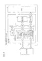
- FIG. 1 is a functional block diagram illustrating an internal configuration of a memory device according to a first embodiment
- FIG. 2 is a timing chart for explaining an example of communication procedure during writing
- FIG. 3 is a timing chart for explaining another example of communication procedure during writing
- FIG. 4 is a flowchart illustrating reception processing of RTT UPIU according to the first embodiment
- FIG. 5 is a timing chart for explaining an example of communication procedure during writing according to the first embodiment
- FIG. 6 is a flowchart illustrating reception processing of RTT UPIU according to a second embodiment
- FIG. 7 is a functional block diagram illustrating an internal configuration of a memory device according to a third embodiment.
- FIG. 8 is a flowchart illustrating reception processing of RTT UPIU according to the third embodiment.
- a memory device includes a nonvolatile first memory, a second memory, an interface unit, and a controller.
- the controller is configured to control the interface unit. when receiving a first packet from the interface unit, the controller transmits a second packet to an initiator via the interface unit, the first packet being a write command received from the initiator, the second packet requesting data transfer to the initiator, the second packet specifying content of a third packet.
- the interface unit includes a comparison unit configured to compare the second packet transmitted to the initiator with a header of the third packet received from the initiator, the third packet including the header and data.
- the controller In the case where the header of the third packet matches the second packet, the controller temporarily stores the third packet to the second memory, and writes the data of the temporarily stored third packet to the first memory. In the case where the header of the third packet does not match the second packet, the controller does not store the third packet to the second memory, the third packet being discarded.
- FIG. 1 is a block diagram illustrating an example of internal configuration of a target 1 which is a memory device according to a first embodiment to which UFS standard is applied.
- the target 1 is connected to an initiator 2 , serving as a host, via a communication path 20 , and functions as an external storage device of the initiator 2 .
- the target 1 and the initiator 2 are based on UFS standard.
- the initiator 2 is, for example, a cellphone, a personal computer, or an imaging device.
- the target 1 includes a controller 3 and a NAND-type flash memory (hereinafter abbreviated as NAND) 4 serving as a nonvolatile memory.
- the NAND 4 includes one or more memory chips having memory cell arrays.
- the memory cell array has a plurality of memory cells arranged in a matrix form.
- Each of memory cell arrays has a plurality of blocks arranged therein, the blocks are units of erasing of data.
- Each block includes a plurality of pages.
- the page is the minimum unit of reading and writing.
- the controller 3 executes data transfer control between the initiator 2 and the NAND 4 .
- the nonvolatile memory 4 is not limited to a NAND flash.
- the nonvolatile memory 4 may be three-dimensional structure flash memory, ReRAM (Resistance Random Access Memory)), FeRAM (Ferroelectric Random Access Memory), a hard disk, and the like.
- the initiator 2 issues a write command and write data to the target 1 .
- the initiator 2 issues a read command to the target 1 .
- the write command, the read command, and the write data is transmitted, as a packet based on UFS standard, to the initiator 2 .
- the target 1 includes an initiator interface 5 , an internal memory 6 , a NAND interface 7 , a CPU (processor) 8 , and a bus 9 .
- the initiator I/F 5 transmits and receives a command packet and data packet to/from the initiator 2 via the communication path 20 .
- the initiator I/F 5 includes a reception unit 10 , and receives a packet from the initiator 2 .
- the initiator I/F 5 includes a transmission unit 11 , and transmits a packet to the initiator 2 .
- a packet will be referred to as UPIU.
- the NAND I/F 7 executes the write control to NAND 4 , and the read control from the NAND 4 .
- the internal memory 6 is a memory allowing for a higher speed access than the NAND 4 .
- the internal memory 6 has a storage area for temporarily storing the data before data received from the initiator 2 are written to the NAND 4 via the NAND I/F 7 .
- the internal memory 6 has a storage area for temporarily storing data read from the NAND 4 via the NAND I/F 7 .
- the internal memory 6 has a storage area for storing and updating management information for managing the target 1 .
- the management information includes a mapping table indicating relationship between a logical address designated by the initiator 2 and a storage position (physical address) on the NAND 4 .
- the management information is backed up by the NAND 4 .
- the SRAM Static Random Access Memory
- DRAM Dynamic Random Access Memory
- the CPU 8 achieves the function by executing the firmware.
- the CPU 8 totally controls internal constituent elements of the target 1 .
- the CPU 8 controls transmission/reception of UPIU between the initiator 2 and the initiator I/F 5 .
- the CPU 8 reads a command received by the reception unit 10 of the initiator I/F 5 , and executes processing according to the read command.
- the CPU 9 controls the initiator I/F 5 to temporarily store the write data to the internal memory 6 .
- the CPU 8 reads the write data from the internal memory 6 , and writes the read data to the NAND 4 via the NAND I/F 7 .
- the CPU 8 updates the management information in the internal memory 6 in accordance with the write processing.
- the CPU 8 When the read command is received from the initiator 2 , the CPU 8 identifies the position on the NAND 4 designated by the read command on the basis of the management information, and reads data from the NAND 4 on the basis of the identified position information.
- the read data is temporarily stored to the internal memory 6 via the NAND I/F 7 , and thereafter, the read data is transmitted via the transmission unit 11 of the initiator I/F 5 to the initiator 2 .
- a Command UPIU is used as a request of reading and writing given by the initiator 2 .
- the Command UPIU includes a field of a logical address and a field of size information (data length).
- the Response UPIU is a UPIU issued by the target 1 when the execution of the processing requested by the initiator 2 with the Command UPIU has been finished. More specifically, when the processing requested by the Command UPIU is finished, the target 1 transmits a Response UPIU corresponding to the Command UPIU.
- the transfer of data between the initiator 2 and the target 1 is executed such that the data is divided into small data in a size DS.
- the Data In UPIU is used to transfer read data from the target 1 to the initiator 2 . More specifically, the Data In UPIU is an UPIU issued by the target 1 when the divided small data is transferred from the target 1 to the initiator 2 .
- a Ready To Transfer UPIU (hereinafter abbreviated as RTT UPIU) is a UPIU issued by the target 1 every time it is ready to receive divided small data.
- RTT UPIU is a UPIU issued by the target 1 every time it is ready to receive divided small data.
- a Data Out UPIU is used when write data is transferred from the initiator 2 to the target 1 .
- a Data Out UPIU is a UPIU issued by the initiator 2 when divided small data is transferred from the initiator 2 to the target 1 .
- the divided small data is transferred as a payload of the Data In UPIU or the Data Out UPIU through the communication path 20 .
- FIG. 2 is a timing chart for explaining an example of communication procedure during writing.
- the initiator 2 transmits a write command in a format of Command UPIU to the target 1 .
- the write command includes a field of Logical Unit Number (LUN), a field of Task Tag, a field of logical address, a field of data length, and the like.
- the LUN designates a partition number on the NAND 4 .
- the Task Tag is information for identifying the Command UPIU.
- the target 1 When the target 1 receives the write command, an area for receiving the write data is assigned in the internal memory 6 . And when the target 1 is ready to receive the data, the target 1 transmits the RTT UPIU to the initiator 2 .
- the RTT UPIU includes LUN, Task Tag, data size DS, and write address WAD.
- the LUN and the Task Tag included in the RTT UPIU are the same as the LUN and the Task Tag included in the corresponding write command UPIU from the initiator 2 .
- the data size DS is a data size that can be currently received by the target 1 , and indicates the size of the divided small data.
- the write address indicates the logical address at the head of the divided small data.
- the initiator 2 extracts, from the write data designated by the write command, data starting from the write address WAD and having a size designated by the data size DS, and transmits the extracted data to the target 1 , using the Data Out UPIU as a header.
- the Data Out UPIU includes the same LUN, Task Tag, data size DS, and write address WAD as the LUN, Task Tag, data size DS, and write address WAD included in the corresponding RTT UPIU.
- RTT UPIU requests data transfer to the initiator and specifies contents of Data Out UPIU.
- the target 1 When the target 1 receives this Data Out UPIU, the target 1 buffers the data included in the payload of the Data Out UPIU to the internal memory 6 . The transmission and the reception of the RTT UPIU and the divided small data are repeated until the transfer of all the write data designated by the write command has been finished.
- the data size DS designated by the RTT UPIU may be different for each RTT UPIU.
- the target 1 When the target 1 receives all the data to be written, the target 1 transmits the Response UPIU to the initiator 2 .
- the LUN and the Task Tag included in the Response UPIU are the same as the LUN and the Task Tag included in the corresponding write command UPIU from the initiator 2 .
- FIG. 3 is a timing chart for explaining another example of communication procedure during writing.
- up to N RTT UPIUs can be transmitted continuously.
- N is 2.
- the communication between the initiator 2 and the target 1 determines that up to N RTT UPIUs can be transmitted continuously.
- the target 1 transmits two RTT UPIUs continuously to the initiator 2 .
- the initiator 2 transmits two Data Out UPIUs continuously to the target 1 .
- information included in the RTT UPIU and header information in the Data Out UPIU actually received may be different. Such situation may occur in a case where there is discrepancy between the processing contents of the initiator 2 and the target 1 .
- the initiator 2 interrupts writing of data corresponding to the write command, and before the interruption processing of the initiator 2 is completed, processing of another write command is performed. In this case, discrepancy occurs between the information of the RTT UPIU and the header information of the Data Out UPIU.
- the target 1 is a slave for the initiator 2 , and therefore, the reception operation cannot be kept waiting.
- the internal memory 6 also stores data included in the Data Out UPIU having a header different from the RTT UPIU commanded by the initiator 2 . For this reason, even if it thereafter tries to receive normal Data Out UPIU, the normal Data Out UPIU may not be received because of the shortage of the internal memory 6 .
- the target 1 saves a history of the transmitted RTT UPIU, and compares header of the received Data Out UPIU with the saved history of the RTT UPIU, and does not store, to the internal memory 6 , the Data Out UPIU that does not match the history of the RTT UPIU saved, and discards the Data Out UPIU.
- the reception unit 10 of the initiator I/F 5 includes an RTT storing unit 12 and an RTT comparator 13 .
- the CPU 8 generates one or more RTT UPIUs on the basis of the write command in the format of the Command UPIU received from the initiator 2 , and inputs the generated RTT UPIU into the transmission unit 11 .
- the transmission unit 11 transmits the RTT UPIU to the initiator 2 , and outputs the transmitted RTT UPIU to the reception unit 10 .
- the RTT storing unit 12 stores the transmitted RTT UPIU which is input from the transmission unit 11 .
- the RTT comparator 13 compares the header of the Data Out UPIU received from the initiator 2 with the RTT UPIU stored in the RTT storing unit 12 . When the header is determined to match therewith by the RTT comparator 13 , the matching RTT UPIU is deleted from the RTT storing unit 12 .
- the RTT storing unit 12 store only a single RTT UPIU, and therefore, there is only one RTT UPIU which is to be compared with the Data Out UPIU in the RTT comparator.
- up to N RTT UPIUs can be transmitted continuously as illustrated in FIG. 3 , the RTT storing unit 12 stores up to N RTT UPIUs.
- the UFS communication does not permit overtaking of Data Out UPIU.
- the overtaking of the Data Out UPIU means a Data Out 2 is received earlier than a Data Out 1 by the target 1 in FIG. 3 .
- FIG. 4 is a flowchart illustrating reception processing of RTT UPIU by the reception unit 10 .
- the reception unit 10 receives the header of a Data Out UPIU (step S 100 ).
- the RTT comparator 13 compares the header of the received Data Out UPIU with the comparison target RTT UPIU stored in the RTT storing unit 12 (step S 110 ). In this comparison, the LUN, the Task Tag, the data size DS, and the write address WAD in the UPIU are compared.
- the reception unit 10 stores the payload of the received Data Out UPIU to the internal memory 6 , and deletes the matching RTT UPIU from the RTT storing unit 12 (step S 120 ). However, when the comparison result does not match in step S 110 , the reception unit 10 does not store the payload of the received Data Out UPIU to the internal memory 6 , and discards the payload (step S 130 ).
- FIG. 5 is a timing chart for explaining an example of communication procedure during writing according to the present embodiment.
- the initiator 2 transmits the write command in the format of the Command UPIU to the target 1 .
- the write command includes the field of the LUN, the field of the Task Tag, the field of the logical address, the field of the data length, and the like.
- the target 1 When the target 1 receives the write command, an area for receiving the write data is assigned in the internal memory 6 , and when it is ready to receive data, the RTT UPIU 1 is transmitted to the initiator 2 .
- the RTT UPIU 1 includes the LUN, the Task Tag, the data size DS, and the write address WAD.
- the transmitted RTT UPIU is temporarily stored in the RTT storing unit 12 .
- the initiator 2 transmits a Data Out UPIU X having a header different from the RTT UPIU 1 .
- the reception unit 10 of the target 1 compares the RTT UPIU 1 temporarily stored in the RTT storing unit 12 as described above with the header of the received Data Out UPIU X. This comparison does not match, and therefore, the payload of the Data Out UPIU X is not stored to the internal memory 6 , and is discarded. Thereafter, when the Data Out UPIU 1 having the header matching the RTT UPIU 1 is received, the payload of this Data Out UPIU 1 is stored to the internal memory 6 .
- an abort request of write command may be transmitted from the initiator 2 .
- the target 1 transmits the RTT UPIU corresponding to the write command to the initiator 2 .
- the initiator 2 cannot send the data corresponding to the RTT UPIU. In such case, the initiator 2 issues an abort request of the write command to the target 1 .
- the RTT UPIU corresponding to the abort request is deleted from the RTT storing unit 12 . For this reason, thereafter, only the normal Data Out UPIU, which is scheduled, can be received. By the way, when the aborted Data Out UPIU is transmitted by the initiator 2 by mistake, this does not match the RTT transmission history stored in the RTT storing unit 12 , and therefore the data is discarded.
- FIG. 6 is a flowchart illustrating reception processing of RTT UPIU in a reception unit 10 according to the second embodiment.
- the processing contents in steps S 100 to S 130 are the same processing contents in steps S 100 to S 130 as illustrated in FIG. 4 , and repeated explanation is omitted.
- step S 110 when the comparison result does not match in step S 110 , the reception unit 10 does not store the payload of the received Data Out UPIU to the internal memory 6 , and discards the payload (step S 130 ). Subsequently, the initiator I/F 5 notifies the interruption to the CPU 8 (step S 141 ). In response to this notification, the CPU 8 stops the write processing (step S 142 ). The CPU 8 transmits the Response UPIU, notifying that the writing has failed, to the initiator 2 via the transmission unit 11 of the initiator I/F 5 (step S 143 ).
- the target 1 uses the Response UPIU in response to the write command to notify the initiator 2 that the writing has failed, and this allows efficient recovery back to normal communication.
- FIG. 7 is a block diagram illustrating an example of internal configuration of the target 1 according to the third embodiment.
- an RTT transmission FIFO 15 is added to the transmission unit 11 of FIG. 1 .
- the RTT transmission FIFO 15 stores multiple RTT UPIUs, which are to be transmitted to the initiator 2 , in accordance with FIFO (First in First out) method. More specifically, the RTT UPIUs generated by the CPU 8 are successively stored to the RTT transmission FIFO 15 .
- FIFO First in First out
- FIG. 8 is a flowchart illustrating reception processing of RTT UPIU in the reception unit 10 according to the third embodiment.
- the processing contents in steps S 100 to S 130 are the same processing contents in steps S 100 to S 130 as illustrated in FIG. 4 , and repeated explanation is omitted.
- the reception unit 10 stores the payload of the received Data Out UPIU to the internal memory 6 , and deletes the matching RTT UPIU from the RTT storing unit 12 (step S 120 ).
- the transmission unit 11 determines whether an RTT UPIU, which is to be subsequently transmitted, is stored in the RTT transmission FIFO 15 or not (step S 150 ).
- step S 150 When the determination result in step S 150 is Yes, the transmission unit 11 transmits a subsequent RTT UPIU stored in the RTT transmission FIFO 15 to the initiator 2 (step S 150 ). When the determination result in step S 150 is Yes, the transmission unit 11 terminates the processing.
- the target 1 when the normal Data Out UPIU is received, the target 1 transmits the subsequent RTT UPIU, and therefore, the RTT UPIU can be transmitted efficiently.
Landscapes
- Engineering & Computer Science (AREA)
- Theoretical Computer Science (AREA)
- Human Computer Interaction (AREA)
- Physics & Mathematics (AREA)
- General Engineering & Computer Science (AREA)
- General Physics & Mathematics (AREA)
- Communication Control (AREA)
- Information Retrieval, Db Structures And Fs Structures Therefor (AREA)
Abstract
Description
Claims (18)
Priority Applications (1)
| Application Number | Priority Date | Filing Date | Title |
|---|---|---|---|
| US14/580,788 US10146475B2 (en) | 2014-09-09 | 2014-12-23 | Memory device performing control of discarding packet |
Applications Claiming Priority (2)
| Application Number | Priority Date | Filing Date | Title |
|---|---|---|---|
| US201462047929P | 2014-09-09 | 2014-09-09 | |
| US14/580,788 US10146475B2 (en) | 2014-09-09 | 2014-12-23 | Memory device performing control of discarding packet |
Publications (2)
| Publication Number | Publication Date |
|---|---|
| US20160070470A1 US20160070470A1 (en) | 2016-03-10 |
| US10146475B2 true US10146475B2 (en) | 2018-12-04 |
Family
ID=55437549
Family Applications (1)
| Application Number | Title | Priority Date | Filing Date |
|---|---|---|---|
| US14/580,788 Active 2035-12-13 US10146475B2 (en) | 2014-09-09 | 2014-12-23 | Memory device performing control of discarding packet |
Country Status (1)
| Country | Link |
|---|---|
| US (1) | US10146475B2 (en) |
Families Citing this family (8)
| Publication number | Priority date | Publication date | Assignee | Title |
|---|---|---|---|---|
| US8228753B2 (en) * | 2009-07-29 | 2012-07-24 | Stec, Inc. | System and method of maintaining data integrity in a flash storage device |
| US10423568B2 (en) * | 2015-12-21 | 2019-09-24 | Microsemi Solutions (U.S.), Inc. | Apparatus and method for transferring data and commands in a memory management environment |
| US10684955B2 (en) * | 2017-04-21 | 2020-06-16 | Micron Technology, Inc. | Memory devices and methods which may facilitate tensor memory access with memory maps based on memory operations |
| KR102395190B1 (en) | 2017-07-31 | 2022-05-06 | 삼성전자주식회사 | Storage Device performing interface with host and Operating Method of Host and Storage Device |
| US10545685B2 (en) | 2017-08-30 | 2020-01-28 | Micron Technology, Inc. | SLC cache management |
| US10712976B2 (en) * | 2017-10-02 | 2020-07-14 | Western Digital Technologies, Inc. | Storage protection unit |
| US10956315B2 (en) | 2018-07-24 | 2021-03-23 | Micron Technology, Inc. | Memory devices and methods which may facilitate tensor memory access |
| US12298902B2 (en) | 2022-08-31 | 2025-05-13 | Samsung Electronics Co., Ltd. | Storage device including nonvolatile memory device and operating method of storage device |
Citations (8)
| Publication number | Priority date | Publication date | Assignee | Title |
|---|---|---|---|---|
| US20050254070A1 (en) * | 2004-05-14 | 2005-11-17 | Katsumi Sayama | Image output apparatus |
| US20090248942A1 (en) * | 2008-03-31 | 2009-10-01 | Lsi Corporation | Posted Memory Write Verification |
| JP2010009472A (en) | 2008-06-30 | 2010-01-14 | Ochanomizu Univ | Network system, control method for network system, and control program |
| US20130036339A1 (en) | 2011-08-01 | 2013-02-07 | Atsushi Shiraishi | Memory device |
| US20130073793A1 (en) * | 2011-09-16 | 2013-03-21 | Osamu Yamagishi | Memory device |
| US20130073795A1 (en) | 2011-09-21 | 2013-03-21 | Misao HASEGAWA | Memory device and method of controlling the same |
| US20130145105A1 (en) * | 2007-06-22 | 2013-06-06 | Antoni SAWICKI | Data Storage Systems and Methods |
| US20140330924A1 (en) * | 2012-10-01 | 2014-11-06 | Edgecast Networks, Inc. | Efficient Cache Validation and Content Retrieval in a Content Delivery Network |
-
2014
- 2014-12-23 US US14/580,788 patent/US10146475B2/en active Active
Patent Citations (11)
| Publication number | Priority date | Publication date | Assignee | Title |
|---|---|---|---|---|
| US20050254070A1 (en) * | 2004-05-14 | 2005-11-17 | Katsumi Sayama | Image output apparatus |
| US20130145105A1 (en) * | 2007-06-22 | 2013-06-06 | Antoni SAWICKI | Data Storage Systems and Methods |
| US20090248942A1 (en) * | 2008-03-31 | 2009-10-01 | Lsi Corporation | Posted Memory Write Verification |
| JP2010009472A (en) | 2008-06-30 | 2010-01-14 | Ochanomizu Univ | Network system, control method for network system, and control program |
| US20130036339A1 (en) | 2011-08-01 | 2013-02-07 | Atsushi Shiraishi | Memory device |
| JP2013050938A (en) | 2011-08-01 | 2013-03-14 | Toshiba Corp | Memory device |
| US20130073793A1 (en) * | 2011-09-16 | 2013-03-21 | Osamu Yamagishi | Memory device |
| JP2013077278A (en) | 2011-09-16 | 2013-04-25 | Toshiba Corp | Memory device |
| US20130073795A1 (en) | 2011-09-21 | 2013-03-21 | Misao HASEGAWA | Memory device and method of controlling the same |
| JP5547154B2 (en) | 2011-09-21 | 2014-07-09 | 株式会社東芝 | Memory device |
| US20140330924A1 (en) * | 2012-10-01 | 2014-11-06 | Edgecast Networks, Inc. | Efficient Cache Validation and Content Retrieval in a Content Delivery Network |
Also Published As
| Publication number | Publication date |
|---|---|
| US20160070470A1 (en) | 2016-03-10 |
Similar Documents
| Publication | Publication Date | Title |
|---|---|---|
| US10146475B2 (en) | Memory device performing control of discarding packet | |
| US12535969B2 (en) | Memory system and method for controlling nonvolatile memory | |
| US10108372B2 (en) | Methods and apparatuses for executing a plurality of queued tasks in a memory | |
| US20130067147A1 (en) | Storage device, controller, and read command executing method | |
| US20210004165A1 (en) | Dummy Host Command Generation For Supporting Higher Maximum Data Transfer Sizes (MDTS) | |
| US20150253992A1 (en) | Memory system and control method | |
| US11340806B2 (en) | Meta data processing during startup of storage devices | |
| US10789167B2 (en) | Information processing apparatus and method for controlling storage device | |
| US20180260145A1 (en) | Internal system namespace exposed through control memory buffer | |
| US20140237170A1 (en) | Storage device, and read command executing method | |
| US20120144094A1 (en) | Data storage apparatus and method for controlling flash memory | |
| US9575887B2 (en) | Memory device, information-processing device and information-processing method | |
| US11698854B2 (en) | Global extension of a logical-to-physical region of a data storage device | |
| US12430080B2 (en) | Method for dynamic management of command queues in synchronous write operations | |
| US9971522B2 (en) | Memory system and method | |
| US10394727B2 (en) | Semiconductor memory device with data buffering | |
| KR102737438B1 (en) | Memory system and operating method thereof | |
| US9684459B2 (en) | Memory system | |
| CN111356991B (en) | Logical block addressing range conflict crawler | |
| US10268388B2 (en) | Access control method, storage device, and system | |
| CN107229581A (en) | Data storage device and its operating method | |
| US20100325373A1 (en) | Duplexing Apparatus and Duplexing Control Method | |
| US20150242160A1 (en) | Memory system, control method of memory system, and controller | |
| US12019901B2 (en) | Memory system connectable to a host and including a nonvolatile memory and a controller electrically connected to the nonvolatile memory | |
| US10228883B2 (en) | Storage device that postpones completion of read command to begin execution of a non-read command |
Legal Events
| Date | Code | Title | Description |
|---|---|---|---|
| AS | Assignment |
Owner name: KABUSHIKI KAISHA TOSHIBA, JAPAN Free format text: ASSIGNMENT OF ASSIGNORS INTEREST;ASSIGNOR:UCHIDA, DAISUKE;REEL/FRAME:034576/0595 Effective date: 20141215 |
|
| AS | Assignment |
Owner name: TOSHIBA MEMORY CORPORATION, JAPAN Free format text: ASSIGNMENT OF ASSIGNORS INTEREST;ASSIGNOR:KABUSHIKI KAISHA TOSHIBA;REEL/FRAME:043088/0620 Effective date: 20170612 |
|
| STCF | Information on status: patent grant |
Free format text: PATENTED CASE |
|
| AS | Assignment |
Owner name: K.K. PANGEA, JAPAN Free format text: MERGER;ASSIGNOR:TOSHIBA MEMORY CORPORATION;REEL/FRAME:055659/0471 Effective date: 20180801 Owner name: KIOXIA CORPORATION, JAPAN Free format text: CHANGE OF NAME AND ADDRESS;ASSIGNOR:TOSHIBA MEMORY CORPORATION;REEL/FRAME:055669/0001 Effective date: 20191001 Owner name: TOSHIBA MEMORY CORPORATION, JAPAN Free format text: CHANGE OF NAME AND ADDRESS;ASSIGNOR:K.K. PANGEA;REEL/FRAME:055669/0401 Effective date: 20180801 |
|
| MAFP | Maintenance fee payment |
Free format text: PAYMENT OF MAINTENANCE FEE, 4TH YEAR, LARGE ENTITY (ORIGINAL EVENT CODE: M1551); ENTITY STATUS OF PATENT OWNER: LARGE ENTITY Year of fee payment: 4 |