US10124680B1 - Methods and systems for pre-charging on-board charger of vehicle - Google Patents
Methods and systems for pre-charging on-board charger of vehicle Download PDFInfo
- Publication number
- US10124680B1 US10124680B1 US15/635,528 US201715635528A US10124680B1 US 10124680 B1 US10124680 B1 US 10124680B1 US 201715635528 A US201715635528 A US 201715635528A US 10124680 B1 US10124680 B1 US 10124680B1
- Authority
- US
- United States
- Prior art keywords
- cycle
- voltage
- switch
- instantaneous frequency
- board charger
- Prior art date
- Legal status (The legal status is an assumption and is not a legal conclusion. Google has not performed a legal analysis and makes no representation as to the accuracy of the status listed.)
- Active, expires
Links
Images


Classifications
-
- B60L11/1811—
-
- H—ELECTRICITY
- H02—GENERATION; CONVERSION OR DISTRIBUTION OF ELECTRIC POWER
- H02J—ELECTRIC POWER NETWORKS; CIRCUIT ARRANGEMENTS OR SYSTEMS FOR SUPPLYING OR DISTRIBUTING ELECTRIC POWER; SYSTEMS FOR STORING ELECTRIC ENERGY
- H02J7/00—Circuit arrangements for charging or discharging batteries or for supplying loads from batteries
- H02J7/02—Circuit arrangements for charging or discharging batteries or for supplying loads from batteries for charging batteries from AC mains by converters
-
- B—PERFORMING OPERATIONS; TRANSPORTING
- B60—VEHICLES IN GENERAL
- B60L—PROPULSION OF ELECTRICALLY-PROPELLED VEHICLES; SUPPLYING ELECTRIC POWER FOR AUXILIARY EQUIPMENT OF ELECTRICALLY-PROPELLED VEHICLES; ELECTRODYNAMIC BRAKE SYSTEMS FOR VEHICLES IN GENERAL; MAGNETIC SUSPENSION OR LEVITATION FOR VEHICLES; MONITORING OPERATING VARIABLES OF ELECTRICALLY-PROPELLED VEHICLES; ELECTRIC SAFETY DEVICES FOR ELECTRICALLY-PROPELLED VEHICLES
- B60L3/00—Electric devices on electrically-propelled vehicles for safety purposes; Monitoring operating variables, e.g. speed, deceleration or energy consumption
- B60L3/0023—Detecting, eliminating, remedying or compensating for drive train abnormalities, e.g. failures within the drive train
- B60L3/0046—Detecting, eliminating, remedying or compensating for drive train abnormalities, e.g. failures within the drive train relating to electric energy storage systems, e.g. batteries or capacitors
-
- B—PERFORMING OPERATIONS; TRANSPORTING
- B60—VEHICLES IN GENERAL
- B60L—PROPULSION OF ELECTRICALLY-PROPELLED VEHICLES; SUPPLYING ELECTRIC POWER FOR AUXILIARY EQUIPMENT OF ELECTRICALLY-PROPELLED VEHICLES; ELECTRODYNAMIC BRAKE SYSTEMS FOR VEHICLES IN GENERAL; MAGNETIC SUSPENSION OR LEVITATION FOR VEHICLES; MONITORING OPERATING VARIABLES OF ELECTRICALLY-PROPELLED VEHICLES; ELECTRIC SAFETY DEVICES FOR ELECTRICALLY-PROPELLED VEHICLES
- B60L53/00—Methods of charging batteries, specially adapted for electric vehicles; Charging stations or on-board charging equipment therefor; Exchange of energy storage elements in electric vehicles
- B60L53/20—Methods of charging batteries, specially adapted for electric vehicles; Charging stations or on-board charging equipment therefor; Exchange of energy storage elements in electric vehicles characterised by converters located in the vehicle
-
- B—PERFORMING OPERATIONS; TRANSPORTING
- B60—VEHICLES IN GENERAL
- B60L—PROPULSION OF ELECTRICALLY-PROPELLED VEHICLES; SUPPLYING ELECTRIC POWER FOR AUXILIARY EQUIPMENT OF ELECTRICALLY-PROPELLED VEHICLES; ELECTRODYNAMIC BRAKE SYSTEMS FOR VEHICLES IN GENERAL; MAGNETIC SUSPENSION OR LEVITATION FOR VEHICLES; MONITORING OPERATING VARIABLES OF ELECTRICALLY-PROPELLED VEHICLES; ELECTRIC SAFETY DEVICES FOR ELECTRICALLY-PROPELLED VEHICLES
- B60L58/00—Methods or circuit arrangements for monitoring or controlling batteries or fuel cells, specially adapted for electric vehicles
- B60L58/10—Methods or circuit arrangements for monitoring or controlling batteries or fuel cells, specially adapted for electric vehicles for monitoring or controlling batteries
- B60L58/12—Methods or circuit arrangements for monitoring or controlling batteries or fuel cells, specially adapted for electric vehicles for monitoring or controlling batteries responding to state of charge [SoC]
- B60L58/15—Preventing overcharging
-
- H02J7/0068—
-
- H02J7/022—
-
- H—ELECTRICITY
- H02—GENERATION; CONVERSION OR DISTRIBUTION OF ELECTRIC POWER
- H02J—ELECTRIC POWER NETWORKS; CIRCUIT ARRANGEMENTS OR SYSTEMS FOR SUPPLYING OR DISTRIBUTING ELECTRIC POWER; SYSTEMS FOR STORING ELECTRIC ENERGY
- H02J7/00—Circuit arrangements for charging or discharging batteries or for supplying loads from batteries
- H02J7/02—Circuit arrangements for charging or discharging batteries or for supplying loads from batteries for charging batteries from AC mains by converters
- H02J7/04—Regulation of charging current or voltage
-
- H02J7/045—
-
- H—ELECTRICITY
- H02—GENERATION; CONVERSION OR DISTRIBUTION OF ELECTRIC POWER
- H02J—ELECTRIC POWER NETWORKS; CIRCUIT ARRANGEMENTS OR SYSTEMS FOR SUPPLYING OR DISTRIBUTING ELECTRIC POWER; SYSTEMS FOR STORING ELECTRIC ENERGY
- H02J7/00—Circuit arrangements for charging or discharging batteries or for supplying loads from batteries
- H02J7/34—Parallel operation in networks using both storage and other DC sources, e.g. providing buffering
- H02J7/345—Parallel operation in networks using both storage and other DC sources, e.g. providing buffering using capacitors as storage or buffering devices
-
- H—ELECTRICITY
- H02—GENERATION; CONVERSION OR DISTRIBUTION OF ELECTRIC POWER
- H02J—ELECTRIC POWER NETWORKS; CIRCUIT ARRANGEMENTS OR SYSTEMS FOR SUPPLYING OR DISTRIBUTING ELECTRIC POWER; SYSTEMS FOR STORING ELECTRIC ENERGY
- H02J7/00—Circuit arrangements for charging or discharging batteries or for supplying loads from batteries
- H02J7/60—Circuit arrangements for charging or discharging batteries or for supplying loads from batteries including safety or protection arrangements
- H02J7/62—Circuit arrangements for charging or discharging batteries or for supplying loads from batteries including safety or protection arrangements against overcurrent
-
- H—ELECTRICITY
- H02—GENERATION; CONVERSION OR DISTRIBUTION OF ELECTRIC POWER
- H02J—ELECTRIC POWER NETWORKS; CIRCUIT ARRANGEMENTS OR SYSTEMS FOR SUPPLYING OR DISTRIBUTING ELECTRIC POWER; SYSTEMS FOR STORING ELECTRIC ENERGY
- H02J7/00—Circuit arrangements for charging or discharging batteries or for supplying loads from batteries
- H02J7/865—Battery or charger load switching, e.g. concurrent charging and load supply
-
- B—PERFORMING OPERATIONS; TRANSPORTING
- B60—VEHICLES IN GENERAL
- B60L—PROPULSION OF ELECTRICALLY-PROPELLED VEHICLES; SUPPLYING ELECTRIC POWER FOR AUXILIARY EQUIPMENT OF ELECTRICALLY-PROPELLED VEHICLES; ELECTRODYNAMIC BRAKE SYSTEMS FOR VEHICLES IN GENERAL; MAGNETIC SUSPENSION OR LEVITATION FOR VEHICLES; MONITORING OPERATING VARIABLES OF ELECTRICALLY-PROPELLED VEHICLES; ELECTRIC SAFETY DEVICES FOR ELECTRICALLY-PROPELLED VEHICLES
- B60L2210/00—Converter types
- B60L2210/10—DC to DC converters
-
- B—PERFORMING OPERATIONS; TRANSPORTING
- B60—VEHICLES IN GENERAL
- B60L—PROPULSION OF ELECTRICALLY-PROPELLED VEHICLES; SUPPLYING ELECTRIC POWER FOR AUXILIARY EQUIPMENT OF ELECTRICALLY-PROPELLED VEHICLES; ELECTRODYNAMIC BRAKE SYSTEMS FOR VEHICLES IN GENERAL; MAGNETIC SUSPENSION OR LEVITATION FOR VEHICLES; MONITORING OPERATING VARIABLES OF ELECTRICALLY-PROPELLED VEHICLES; ELECTRIC SAFETY DEVICES FOR ELECTRICALLY-PROPELLED VEHICLES
- B60L2210/00—Converter types
- B60L2210/30—AC to DC converters
-
- H—ELECTRICITY
- H02—GENERATION; CONVERSION OR DISTRIBUTION OF ELECTRIC POWER
- H02J—ELECTRIC POWER NETWORKS; CIRCUIT ARRANGEMENTS OR SYSTEMS FOR SUPPLYING OR DISTRIBUTING ELECTRIC POWER; SYSTEMS FOR STORING ELECTRIC ENERGY
- H02J2105/00—Networks for supplying or distributing electric power characterised by their spatial reach or by the load
- H02J2105/30—Networks for supplying or distributing electric power characterised by their spatial reach or by the load the load networks being external to vehicles, i.e. exchanging power with vehicles
- H02J2105/33—Networks for supplying or distributing electric power characterised by their spatial reach or by the load the load networks being external to vehicles, i.e. exchanging power with vehicles exchanging power with road vehicles
- H02J2105/37—Networks for supplying or distributing electric power characterised by their spatial reach or by the load the load networks being external to vehicles, i.e. exchanging power with vehicles exchanging power with road vehicles exchanging power with electric vehicles [EV] or with hybrid electric vehicles [HEV]
-
- H—ELECTRICITY
- H02—GENERATION; CONVERSION OR DISTRIBUTION OF ELECTRIC POWER
- H02J—ELECTRIC POWER NETWORKS; CIRCUIT ARRANGEMENTS OR SYSTEMS FOR SUPPLYING OR DISTRIBUTING ELECTRIC POWER; SYSTEMS FOR STORING ELECTRIC ENERGY
- H02J2207/00—Details of circuit arrangements for charging or discharging batteries or supplying loads from batteries
- H02J2207/20—Charging or discharging characterised by the power electronics converter
-
- H—ELECTRICITY
- H02—GENERATION; CONVERSION OR DISTRIBUTION OF ELECTRIC POWER
- H02J—ELECTRIC POWER NETWORKS; CIRCUIT ARRANGEMENTS OR SYSTEMS FOR SUPPLYING OR DISTRIBUTING ELECTRIC POWER; SYSTEMS FOR STORING ELECTRIC ENERGY
- H02J7/00—Circuit arrangements for charging or discharging batteries or for supplying loads from batteries
- H02J7/90—Regulation of charging or discharging current or voltage
- H02J7/927—Regulation of charging or discharging current or voltage with introduction of pulses during the charging process
-
- Y—GENERAL TAGGING OF NEW TECHNOLOGICAL DEVELOPMENTS; GENERAL TAGGING OF CROSS-SECTIONAL TECHNOLOGIES SPANNING OVER SEVERAL SECTIONS OF THE IPC; TECHNICAL SUBJECTS COVERED BY FORMER USPC CROSS-REFERENCE ART COLLECTIONS [XRACs] AND DIGESTS
- Y02—TECHNOLOGIES OR APPLICATIONS FOR MITIGATION OR ADAPTATION AGAINST CLIMATE CHANGE
- Y02T—CLIMATE CHANGE MITIGATION TECHNOLOGIES RELATED TO TRANSPORTATION
- Y02T10/00—Road transport of goods or passengers
- Y02T10/60—Other road transportation technologies with climate change mitigation effect
- Y02T10/70—Energy storage systems for electromobility, e.g. batteries
-
- Y—GENERAL TAGGING OF NEW TECHNOLOGICAL DEVELOPMENTS; GENERAL TAGGING OF CROSS-SECTIONAL TECHNOLOGIES SPANNING OVER SEVERAL SECTIONS OF THE IPC; TECHNICAL SUBJECTS COVERED BY FORMER USPC CROSS-REFERENCE ART COLLECTIONS [XRACs] AND DIGESTS
- Y02—TECHNOLOGIES OR APPLICATIONS FOR MITIGATION OR ADAPTATION AGAINST CLIMATE CHANGE
- Y02T—CLIMATE CHANGE MITIGATION TECHNOLOGIES RELATED TO TRANSPORTATION
- Y02T10/00—Road transport of goods or passengers
- Y02T10/60—Other road transportation technologies with climate change mitigation effect
- Y02T10/7072—Electromobility specific charging systems or methods for batteries, ultracapacitors, supercapacitors or double-layer capacitors
-
- Y—GENERAL TAGGING OF NEW TECHNOLOGICAL DEVELOPMENTS; GENERAL TAGGING OF CROSS-SECTIONAL TECHNOLOGIES SPANNING OVER SEVERAL SECTIONS OF THE IPC; TECHNICAL SUBJECTS COVERED BY FORMER USPC CROSS-REFERENCE ART COLLECTIONS [XRACs] AND DIGESTS
- Y02—TECHNOLOGIES OR APPLICATIONS FOR MITIGATION OR ADAPTATION AGAINST CLIMATE CHANGE
- Y02T—CLIMATE CHANGE MITIGATION TECHNOLOGIES RELATED TO TRANSPORTATION
- Y02T10/00—Road transport of goods or passengers
- Y02T10/60—Other road transportation technologies with climate change mitigation effect
- Y02T10/72—Electric energy management in electromobility
-
- Y—GENERAL TAGGING OF NEW TECHNOLOGICAL DEVELOPMENTS; GENERAL TAGGING OF CROSS-SECTIONAL TECHNOLOGIES SPANNING OVER SEVERAL SECTIONS OF THE IPC; TECHNICAL SUBJECTS COVERED BY FORMER USPC CROSS-REFERENCE ART COLLECTIONS [XRACs] AND DIGESTS
- Y02—TECHNOLOGIES OR APPLICATIONS FOR MITIGATION OR ADAPTATION AGAINST CLIMATE CHANGE
- Y02T—CLIMATE CHANGE MITIGATION TECHNOLOGIES RELATED TO TRANSPORTATION
- Y02T90/00—Enabling technologies or technologies with a potential or indirect contribution to GHG emissions mitigation
- Y02T90/10—Technologies relating to charging of electric vehicles
- Y02T90/14—Plug-in electric vehicles
Definitions
- the present invention relates to pre-charging an on-board charger (OBC) of a vehicle.
- OBC on-board charger
- An on-board charger (OBC) of an electric vehicle is used for charging a traction battery of the vehicle.
- the OBC charges the battery with electrical power from a mains supply.
- the electrical power from the mains supply is an AC electrical power.
- the battery is to be charged with DC electrical power.
- the OBC has an input which connects to the mains supply for the OBC to receive AC electrical power from the mains supply.
- the OBC converts AC electrical power received from the mains supply into DC electrical power.
- the OBC has an output which connects to the battery.
- the OBC provides the DC electrical power converted from the AC electrical power to the battery for charging the battery.
- the OBC has one or more internal bulk capacitors (collectively “DC link capacitor”).
- the DC link capacitor is charged with the DC electrical power converted from the AC electrical power to have a DC voltage (“DC-link voltage”).
- DC-link voltage In a stable operation mode of the OBC, the DC link voltage is a boosted, constant DC voltage.
- the DC link capacitor is connected to the traction battery through a DC/DC converter and, typically, a disconnection switch.
- the DC/DC converter is used for voltage adaption as the traction battery voltage could vary in a relatively wide range (for instance, 200V-400V) while the DC-link voltage is expected to be constant.
- the DC link capacitor In a pre-charge operation mode of the OBC, the DC link capacitor is to be charged to the boosted, constant DC voltage. At the beginning of the pre-charge operation the DC link voltage is zero volts or a low voltage (i.e., the DC link capacitor is discharged or nearly discharged). The DC link capacitor is to be progressively charged so that inrush electrical currents are avoided. Inrush electrical currents could damage internal components of the OBC or the mains supply.
- An object is a pre-charge control strategy for an on-board charger (OBC).
- OBC on-board charger
- Another object is a soft-start control strategy in a vehicle OBC to minimize input inrush electrical current peaks.
- Another object is a soft-start control strategy in a vehicle OBC to provide immunity from domestic network (i.e., mains supply) noise.
- Another object is to provide a soft charge of internal bulk capacitor(s) (i.e., the DC link capacitor) of a vehicle OBC by controlled triggering of power switches of the OBC to avoid inrush electrical current which may otherwise damage the domestic network or components of the OBC.
- internal bulk capacitor(s) i.e., the DC link capacitor
- the OBC includes a switch configured to receive an AC voltage having a plurality of cycles each including an odd half-cycle and an even half-cycle, a capacitor connected to the switch and connectable to a traction battery of an electric vehicle, a frequency sensor, and a controller.
- the capacitor may be connectable to the traction battery through a DC/DC converter with or without a disconnection element.
- the frequency sensor is configured to detect during the odd half-cycle of a first cycle of the AC voltage an instantaneous frequency of the AC voltage for the first cycle based on elapsed time between zero-voltage crossings of the odd half-cycle of the first cycle and not based on any other zero-voltage crossings of the AC voltage.
- the controller is configured to close the switch during the even half-cycle of the first cycle at a first trigger time dependent upon the instantaneous frequency of the AC voltage for the first cycle.
- the capacitor is enabled to be charged with the AC voltage via the switch while the switch is closed.
- This OBC includes a first switch configured to receive an AC voltage having a plurality of cycles each including an odd half-cycle and an even half-cycle, a second switch configured to receive the AC voltage, a capacitor connected to the first switch and to the second switch and connectable to a traction battery of an electric vehicle, a sensor, and a controller.
- the capacitor may be connectable to the traction battery through a DC/DC converter with or without a disconnection element.
- the sensor is configured to detect during the odd half-cycle of a second cycle of the AC voltage an instantaneous frequency of the AC voltage for the odd half-cycle of the second cycle based on elapsed time between a voltage peak of the odd half-cycle of the second cycle and a voltage peak of the even half-cycle of a first cycle of the AC voltage.
- the controller is configured to close the first switch during the odd half-cycle of the second cycle at a first trigger time dependent upon the instantaneous frequency of the AC voltage for the odd half-cycle of the second cycle.
- the capacitor is enabled to be charged with the AC voltage via the first switch while the first switch is closed.
- a method for an OBC includes a switch configured to receive an AC voltage having a plurality of cycles. Each cycle includes an odd half-cycle and an even half-cycle.
- the OBC further includes a capacitor connected to the switch and connectable to a traction battery of an electric vehicle. The capacitor may be connectable to the traction battery through a DC/DC converter with or without a disconnection element.
- the method includes detecting during the odd half-cycle of a first cycle of the AC voltage an instantaneous frequency of the AC voltage for the first cycle based on elapsed time between zero-voltage crossings of the odd half-cycle of the first cycle and not based on any other zero-voltage crossings of the AC voltage.
- the method further includes closing the switch during the even half-cycle of the first cycle at a first trigger time dependent upon the instantaneous frequency of the AC voltage for the first cycle, wherein the capacitor is enabled to be charged with the AC voltage via the switch while the switch is closed.
- the method may further include detecting during the odd half-cycle of a second cycle of the AC voltage an instantaneous frequency of the AC voltage for the second cycle based on elapsed time between zero-voltage crossings of the odd half-cycle of the second cycle and not based on any other zero-voltage crossings of the AC voltage, and closing the switch during the even half-cycle of the second cycle at a second trigger time dependent upon the instantaneous frequency of the AC voltage for the second cycle.
- FIG. 1 illustrates a circuit and block diagram of an on-board charger (OBC);
- OBC on-board charger
- FIG. 2 illustrates a graph of a (rectified) input AC voltage v in (t) inputted to a rectifier of the OBC and three different resulting capacitor voltages v c (t) of an output DC link capacitor of the OBC during a pre-charge operation of the DC link capacitor in which the OBC progressively charges the DC link capacitor using electrical power from the input AC voltage;
- FIG. 3 illustrates a block diagram depicting steps of a pre-charging operation mode of the OBC for charging the DC link capacitor to a boosted, constant DC voltage
- FIG. 4 illustrates a graph of two cycles of the (rectified) input AC voltage v in (t) inputted to a rectifier of the OBC, a first set of time-periods that a thyristor of the rectifier is to be activated in the two cycles for charging the DC link capacitor per a first pre-determined capacitor voltage profile, and a second set of time-periods that the thyristor is to be activated in the two cycles for charging the DC link capacitor per a second pre-determined capacitor voltage profile;
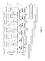
- FIG. 5 illustrates graphs depicting operation of a sequential measure-triggering strategy for pre-charging the DC link capacitor in accordance with embodiments of the present invention
- FIG. 6 illustrates a graph of the input AC voltage v in (t) and a desired pre-determined capacitor voltage profile v out _ desired (t) of the DC link capacitor for explaining when a thyristor is closed and opened during pre-charging of the DC link capacitor;
- FIG. 7 illustrates graphs depicting operation of a pipelined measure-triggering strategy for pre-charging the DC link capacitor in accordance with embodiments of the present invention.
- OBC 10 is on-board an electric vehicle.
- OBC 10 is used for charging a traction battery 12 (or other loads) of the vehicle.
- OBC 10 includes a charger power stage 14 .
- Charger power stage 14 receives AC electrical power from a mains supply (i.e., a domestic network power supply) 16 , converts the received AC electrical power into DC electrical power, and charges traction battery 12 with the DC electrical power through a DC/DC converter 15 and a disconnection element (i.e., a switch) 17 .
- a mains supply i.e., a domestic network power supply
- Charger power stage 14 includes an input filter 18 , a full-bridge rectifier 20 , a power factor converter (PFC) 22 , and a DC link capacitor (“C Bulk ”) 24 .
- Input filter 18 is at the input side of charger power stage 14 .
- Rectifier 20 follows input filter 18 .
- PFC 22 follows rectifier 20 .
- DC link capacitor 24 is at the output side of charger power stage 14 .
- DC link capacitor 24 is one or more bulk capacitors which collectively comprise the DC link capacitor.
- Input filter 18 is connected to mains supply 16 to receive an AC mains voltage (v mains (t)) from the mains supply.
- the AC mains voltage has, for example, a root mean square (rms) voltage in the range of 100 V-240 V and a frequency of 50 or 60 Hz.
- Input filter 18 filters the AC mains voltage to reject high-frequency noise therefrom.
- Input filter 18 outputs the filtered AC mains voltage as an input AC voltage (v in (t)) to rectifier 20 .
- Rectifier 20 rectifies the input AC voltage into an output DC voltage (v out (t)).
- Rectifier 20 includes four rectifying elements connected in a full-bridge (i.e., diamond) configuration.
- the rectifying elements include first and second diodes, D 1 and D 2 , and first and second thyristors, Tr 1 and Tr 2 .
- Thyristors Tr 1 , Tr 2 have triggering input voltages v Tr1 and v Tr2 , respectively.
- the thyristor i.e., a switch
- current cannot flow through the thyristor. That is, the thyristor is opened.
- a conductor connects the thyristors to PFC 22 .
- the cathodes of first thyristor Tr 1 and second thyristor Tr 2 are connected to each other and to PFC 22 .
- the anodes of first diode D 1 and second diode D 2 are connected to each other.
- the cathode of first diode D 1 is connected to the anode of first thyristor Tr 1 and the cathode of second D 2 is connected to the anode of second thyristor Tr 2 .
- PFC 22 is connected in parallel to DC link capacitor 24 .
- Charger power stage 14 further includes a third diode D 3 .
- Third diode D 3 connects rectifier 20 to DC link capacitor 24 while bypassing PFC 22 .
- Third diode D 3 is a bypass for a pre-charge period as explained below.
- DC-link capacitor 24 is connected to the input of DC/DC converter 15 .
- capacitor voltage (vc(t)) of DC link capacitor 24 is an input DC voltage to DC/DC converter 15 .
- the output of DC/DC converter 15 is connected to the traction battery 12 though a disconnection element 17 .
- the capacitor voltage is thus the DC voltage of the DC electrical power provided from charger power stage 14 for charging traction battery 12 .
- OBC 10 has two operation modes: a stable operation mode and a pre-charge operation mode.
- the stable operation mode DC link capacitor 24 is kept charged at a boosted, constant DC voltage.
- PFC 22 receives the output DC voltage v out (t) from rectifier 20 .
- PFC 22 improves AC/DC conversion (e.g., efficiency, smoothness, etc.) of the output DC voltage v out (t).
- PFC 22 includes power switch transistors and the like which are used to improve the AC/DC conversion.
- PFC 22 charges DC link capacitor 24 with the output DC voltage.
- DC link capacitor 24 thus has a capacitor voltage v c (t) from being charged with the output DC voltage.
- DC link capacitor 24 is to be charged to the boosted, constant DC voltage.
- Third diode D 3 is a bypass for the pre-charge period.
- the capacitor voltage of DC link capacitor 24 is zero volts or a low voltage (i.e., the DC link capacitor is discharged or nearly discharged).
- DC link capacitor 24 is to be progressively charged in a way inrush electrical currents are avoided.
- Tr 1 or Tr 2 is ON, the input current i in (t) is a function of the input AC voltage v in (t).
- the charging current flows through third diode D 3 , as PFC 22 , which is mainly inductive, blocks any spurious current flow.
- FIG. 2 a graph 30 of (rectified) input AC voltage v in (t) inputted to rectifier 20 of OBC 10 and three different resulting capacitor voltages v c (t) of DC link capacitor 24 during a pre-charge operation in which the DC link capacitor is progressively charged using electrical power from the input AC voltage is shown.
- Graph 30 includes a plot 32 of input AC voltage v in (t), a plot 34 of a first resulting capacitor voltage v c (t), a plot 36 of a second resulting capacitor voltage v c (t), and a plot 38 of a third resulting capacitor voltage v c (t).
- T mains is the period of the input AC voltage and V mains is the maxim value of the input AC voltage.
- Plot 32 shown in FIG. 2 represents the (rectified) input AC voltage.
- V out _ desired ( t ) V mains *sin 2 [ ⁇ /2 *t/T f ] (3)
- Plots 36 and 38 shown in FIG. 2 represent the resulting capacitor voltage per expressions (2) and (3), respectively.
- T mains and T f are also shown in graph 30 of FIG. 2 .
- OBC 10 further includes a micro-controller (“controller”) 40 , a gate driver 42 for thyristors T 1 and T 2 , and a domestic network (i.e., mains supply) detector 44 .
- Controller 40 is an electronic processor or the like configured to receive sensor signals and generate control signals based on the sensor signals.
- Gate driver 42 is configured to provide triggering input voltages v Tr1 and v Tr2 to thyristors Tr 1 and Tr 2 , respectively.
- Detector 44 is configured to detect (i.e., measure) the instantaneous frequency of the input AC voltage v in (t). Detector 44 can detect zero-voltage crossing times of the input AC voltage to determine the frequency of the input AC voltage. Detector 44 can detect the instantaneous frequency of the input AC voltage based on the immediate previous two zero-voltage crossing times of the input AC voltage. Detector 44 is further configured to detect the instantaneous voltage (e.g., maximum value or rms value) of the input AC voltage.
- the instantaneous voltage e.g., maximum value or rms value
- Controller 40 may control the pre-charging of OBC 10 using the detected frequency and voltage of the input AC voltage v in (t). That is, controller 40 may control gate driver 42 to trigger thyristors Tr 1 and/or Tr 2 at times determined to be appropriate, for the pre-charging of OBC 10 , based on the frequency and voltage of the input AC voltage. Controller 40 may also predict when the next zero-voltage crossing time of the input AC voltage based on the detected frequency of the input AC voltage. Controller 40 may further control the pre-charging of OBC 10 using such predicted next zero-voltage crossing times.
- FIG. 3 a block diagram 50 depicting steps of the pre-charging operation mode of OBC 10 is shown.
- the pre-charging operation mode initiates upon OBC 10 being connected to mains supply 16 as indicated by start point 52 .
- DC link capacitor 24 has zero volts or is charged with relatively little voltage and therefore is to be pre-charged to the boosted DC voltage value for the stable operation mode of OBC 10 to be reached.
- the input AC voltage v in (t) is provided to rectifier 20 of OBC 10 while the OBC is connected to mains supply 16 .
- Controller 40 initially conducts a domestic network (i.e., mains supply) characterization as indicated by block 54 .
- the domestic network characterization involves detector 44 detecting the voltage of the input AC voltage v in (t) as indicated by block 56 .
- the domestic network characterization further involves detector 44 detecting the frequency (average value) of the input AC voltage v in (t) as indicated by block 58 .
- Controller 40 receives information regarding the detected voltage and frequency of the input AC voltage v in (t) to be apprised of general characteristics of the input AC voltage (e.g., 120V/60 Hz).
- controller 40 implements a control loop in which the controller controls progressive charging of DC link capacitor 24 until the capacitor voltage v c (t) corresponds to the desired boosted DC voltage value.
- the operation of the control loop includes the capacitor voltage v c (t) being detected as indicated by block 60 .
- Controller compares this detected capacitor voltage v c (t) with the desired boosted DC voltage value to determine whether DC link capacitor 24 is appropriately charged as indicated by decision block 62 .
- DC link capacitor 24 is appropriately charged upon the capacitor voltage v c (t) reaching the desired boosted DC voltage value. If DC link capacitor 24 is appropriately charged, then the control loop ends as indicated by end-point 64 and the stable operation mode of OBC 10 commences.
- each iteration involves detector 44 detecting an instantaneous value of the frequency of the input AC voltage v in (t) as indicated in block 66 , controller 40 determining a trigger time for when a thyristor Tr 1 or Tr 2 is to be triggered as indicated in block 68 , and gate driver 42 triggering the thyristor at the trigger time as indicated in block 70 .
- Controller 40 determines the trigger time based on the detected instantaneous value of the frequency of the input AC voltage. In addition to using the instantaneous value of the frequency of the input AC voltage, controller 40 may also determine the trigger time using a detected voltage (e.g., maxim value or RMS value) of the input AC voltage.
- a detected voltage e.g., maxim value or RMS value
- the input AC voltage v in (t) is provided via the triggered thyristor through rectifier 20 and third diode D 3 to DC link capacitor 24 to charge the DC link capacitor.
- the charging occurs while input AC voltage v in (t) is greater than the capacitor voltage v c (t) until the input AC voltage v in (t) reaches a zero-voltage crossing time.
- the current iteration of the iteration sequence of the control loop terminates at the zero-voltage crossing time of the input AC voltage v in (t). Subsequent iterations of the iteration sequence are repeated until DC link capacitor 24 is appropriately charged.
- Plot 82 represents the (rectified) input AC voltage v in (t)
- plot 84 represents the pre-determined capacitor voltage profile v out _ desired (t) per expression (2)
- plot 86 represents the pre-determined capacitor voltage profile v out _ desired (t) per expression (3).
- v out _ desired (t) is the pre-determined profile of the capacitor voltage v c (t).
- Controller 40 computes the period that the thyristor is to be activated (T pwm _ thy _ #i ) in each cycle of the input AC voltage v in (t) by finding the time interval when v out _ desired (t)>v in (t) in the last part of the cycle (t>T mains /4).
- FIG. 4 shows T pwm _ thy _ #i for two consecutive cycles of V out _ desired (t) marked by plot 84 for expression (3) and marked by plot 86 for expression (4).
- Each T pwm _ thy can be determined by controller 40 during run-time of OBC 10 or can be pre-computed and stored as a look up table in the controller.
- Controller 40 can use different strategies in the case that controller 40 computes the vales of T pwm _ thy _ #i in real-time (no look-up tables used). Two different strategies include a sequential measure-triggering strategy and a pipelined measure-triggering strategy.
- Top graph 90 of FIG. 5 illustrates mathematical functions used to find T pwm _ thy _ #i .
- (Rectified) input AC voltage Abs(v in (t)) based on expression (1) is shown by plot 92 .
- a desired pre-determined capacitor voltage profile v out _ desired (t) (such as per expression (2)) is shown by plot 94 .
- T zc _ time is measured in one semi-cycle (i.e., a half cycle of a full cycle) (named “odd”) and is used in the next semi-cycle (i.e., the other half cycle of the full cycle) (named “even”) to find the interval T pwm _ thy _ #i when the thyristor should be triggered.
- These time intervals also known as activation pulses
- T zc _ time T mains /2.
- Middle graph 100 of FIG. 5 illustrates the actual (rectified) input AC voltage Abs(v in (t)) and the capacitor voltage v c (t). Notice that T zc _ time cannot be measured in “even” semi-cycles because when the thyristor is activated, it “pulls down” the input AC voltage to the DC link capacitor voltage v c (t). Consequently, it is impossible to measure the instant when v in (t) crosses zero. In other words, any frequency measurement based on zero crossing circuitry or minimal value will be affected by the pre-charge process itself. Accordingly, methods and systems in accordance with various embodiments for pre-charging OBC 10 employ separate frequency measurement periods and triggering periods alternatively (alternating measurement and triggering periods) as shown in bottom graph 110 of FIG. 5 .
- the sequential measure-triggering strategy operates as follows.
- the algorithm is executed for each cycle of the input AC voltage, from 1 to Nc. That means the algorithm needs to run from 1 to 2*Nc semi-cycles in total.
- T mains is measured by monitoring the zero-crossing of the input AC voltage v in (t) at the beginning and the end of the semi-cycle.
- V mains is measured by monitoring the maximum value of the input AC voltage during the semi-cycle or by monitoring the rms value of the input AC voltage during the semi-cycle.
- the capacitor voltage v c (t) is approximately constant during the semi-cycle and can therefore be monitored at any time during the semi-cycle.
- each second semi-cycle corresponding to “even” values of the counter of number of semi-cycles, is when the conditions to activate or deactivate the thyristors are done.
- FIG. 6 illustrates a graph 120 of the input AC voltage v in (t) (represented by plot 122 ) and the desired pre-determined capacitor voltage profile v out _ desired (t) (represented by plot 124 ) for explaining when a thyristor is closed and opened during pre-charging of DC link capacitor 24 .
- N step T mains /(2*t step ) */
- FIG. 7 illustrates graphs depicting operation of the pipelined measure-triggering strategy for pre-charging DC link capacitor 24 . This strategy produces faster pre-charges with same current or smaller currents with same pre-charge time as previous strategy.
- Top graph 130 of FIG. 7 illustrates mathematical functions used to find T pwm _ thy _ #i .
- (Rectified) input AC voltage Abs(v in (t)) based on expression (1) is shown by plot 132 .
- a desired pre-determined capacitor voltage profile v out _ desired (t) (such as per expression (3)) is shown by plot 134 .
- the determined time intervals (also known as activation pulses) that thyristor is to be triggered are shown by plots 136 .
- Middle graph 140 of FIG. 5 illustrates the actual (rectified) input AC voltage Abs(v in (t)) and the capacitor voltage v c (t).
- This strategy is named pipelined because measuring of T mains , V mains , and v c (t) is done continuously, in each semi-cycle.
- the pipelined algorithm is similar to the previous sequential algorithm. However, the pipelined algorithm requires specific hardware to make possible to measure T mains and V mains when the trigger is activated. Therefore, the sequential algorithm is preferred for implementation since hardware complexity is reduced.
Landscapes
- Engineering & Computer Science (AREA)
- Power Engineering (AREA)
- Transportation (AREA)
- Mechanical Engineering (AREA)
- Life Sciences & Earth Sciences (AREA)
- Sustainable Development (AREA)
- Sustainable Energy (AREA)
- Rectifiers (AREA)
Abstract
An on-board charger for an electric vehicle includes a switch configured to receive an AC voltage, a capacitor connected to the switch and connectable to a traction battery of the electric vehicle, a frequency sensor, and a controller. The frequency sensor is configured to detect during the odd half-cycle of a first cycle of the AC voltage an instantaneous frequency of the AC voltage for the first cycle based on elapsed time between zero-voltage crossings of the odd half-cycle of the first cycle and not based on any other zero-voltage crossings of the AC voltage. The controller is configured to close the switch during the even half-cycle of the first cycle at a first trigger time dependent upon the instantaneous frequency of the AC voltage for the first cycle. The capacitor is enabled to be charged with the AC voltage via the switch while the switch is closed.
Description
The present invention relates to pre-charging an on-board charger (OBC) of a vehicle.
An on-board charger (OBC) of an electric vehicle is used for charging a traction battery of the vehicle. The OBC charges the battery with electrical power from a mains supply. The electrical power from the mains supply is an AC electrical power. The battery is to be charged with DC electrical power. The OBC has an input which connects to the mains supply for the OBC to receive AC electrical power from the mains supply. The OBC converts AC electrical power received from the mains supply into DC electrical power. The OBC has an output which connects to the battery. The OBC provides the DC electrical power converted from the AC electrical power to the battery for charging the battery.
The OBC has one or more internal bulk capacitors (collectively “DC link capacitor”). The DC link capacitor is charged with the DC electrical power converted from the AC electrical power to have a DC voltage (“DC-link voltage”). In a stable operation mode of the OBC, the DC link voltage is a boosted, constant DC voltage. The DC link capacitor is connected to the traction battery through a DC/DC converter and, typically, a disconnection switch. The DC/DC converter is used for voltage adaption as the traction battery voltage could vary in a relatively wide range (for instance, 200V-400V) while the DC-link voltage is expected to be constant.
In a pre-charge operation mode of the OBC, the DC link capacitor is to be charged to the boosted, constant DC voltage. At the beginning of the pre-charge operation the DC link voltage is zero volts or a low voltage (i.e., the DC link capacitor is discharged or nearly discharged). The DC link capacitor is to be progressively charged so that inrush electrical currents are avoided. Inrush electrical currents could damage internal components of the OBC or the mains supply.
An object is a pre-charge control strategy for an on-board charger (OBC).
Another object is a soft-start control strategy in a vehicle OBC to minimize input inrush electrical current peaks.
Another object is a soft-start control strategy in a vehicle OBC to provide immunity from domestic network (i.e., mains supply) noise.
Another object is to provide a soft charge of internal bulk capacitor(s) (i.e., the DC link capacitor) of a vehicle OBC by controlled triggering of power switches of the OBC to avoid inrush electrical current which may otherwise damage the domestic network or components of the OBC.
An OBC is provided. The OBC includes a switch configured to receive an AC voltage having a plurality of cycles each including an odd half-cycle and an even half-cycle, a capacitor connected to the switch and connectable to a traction battery of an electric vehicle, a frequency sensor, and a controller. The capacitor may be connectable to the traction battery through a DC/DC converter with or without a disconnection element. The frequency sensor is configured to detect during the odd half-cycle of a first cycle of the AC voltage an instantaneous frequency of the AC voltage for the first cycle based on elapsed time between zero-voltage crossings of the odd half-cycle of the first cycle and not based on any other zero-voltage crossings of the AC voltage. The controller is configured to close the switch during the even half-cycle of the first cycle at a first trigger time dependent upon the instantaneous frequency of the AC voltage for the first cycle. The capacitor is enabled to be charged with the AC voltage via the switch while the switch is closed.
Another OBC is provided. This OBC includes a first switch configured to receive an AC voltage having a plurality of cycles each including an odd half-cycle and an even half-cycle, a second switch configured to receive the AC voltage, a capacitor connected to the first switch and to the second switch and connectable to a traction battery of an electric vehicle, a sensor, and a controller. The capacitor may be connectable to the traction battery through a DC/DC converter with or without a disconnection element. The sensor is configured to detect during the odd half-cycle of a second cycle of the AC voltage an instantaneous frequency of the AC voltage for the odd half-cycle of the second cycle based on elapsed time between a voltage peak of the odd half-cycle of the second cycle and a voltage peak of the even half-cycle of a first cycle of the AC voltage. The controller is configured to close the first switch during the odd half-cycle of the second cycle at a first trigger time dependent upon the instantaneous frequency of the AC voltage for the odd half-cycle of the second cycle. The capacitor is enabled to be charged with the AC voltage via the first switch while the first switch is closed.
A method for an OBC is provided. The OBC includes a switch configured to receive an AC voltage having a plurality of cycles. Each cycle includes an odd half-cycle and an even half-cycle. The OBC further includes a capacitor connected to the switch and connectable to a traction battery of an electric vehicle. The capacitor may be connectable to the traction battery through a DC/DC converter with or without a disconnection element. The method includes detecting during the odd half-cycle of a first cycle of the AC voltage an instantaneous frequency of the AC voltage for the first cycle based on elapsed time between zero-voltage crossings of the odd half-cycle of the first cycle and not based on any other zero-voltage crossings of the AC voltage. The method further includes closing the switch during the even half-cycle of the first cycle at a first trigger time dependent upon the instantaneous frequency of the AC voltage for the first cycle, wherein the capacitor is enabled to be charged with the AC voltage via the switch while the switch is closed.
The method may further include detecting during the odd half-cycle of a second cycle of the AC voltage an instantaneous frequency of the AC voltage for the second cycle based on elapsed time between zero-voltage crossings of the odd half-cycle of the second cycle and not based on any other zero-voltage crossings of the AC voltage, and closing the switch during the even half-cycle of the second cycle at a second trigger time dependent upon the instantaneous frequency of the AC voltage for the second cycle.
Detailed embodiments of the present invention are disclosed herein; however, it is to be understood that the disclosed embodiments are merely exemplary of the invention that may be embodied in various and alternative forms. The figures are not necessarily to scale; some features may be exaggerated or minimized to show details of particular components. Therefore, specific structural and functional details disclosed herein are not to be interpreted as limiting, but merely as a representative basis for teaching one skilled in the art to variously employ the present invention.
Referring now to FIG. 1 , a circuit and block diagram of an on-board charger (OBC) 10 is shown. OBC 10 is on-board an electric vehicle. OBC 10 is used for charging a traction battery 12 (or other loads) of the vehicle. OBC 10 includes a charger power stage 14. Charger power stage 14 receives AC electrical power from a mains supply (i.e., a domestic network power supply) 16, converts the received AC electrical power into DC electrical power, and charges traction battery 12 with the DC electrical power through a DC/DC converter 15 and a disconnection element (i.e., a switch) 17.
A conductor connects the thyristors to PFC 22. Specifically, the cathodes of first thyristor Tr1 and second thyristor Tr2 are connected to each other and to PFC 22. The anodes of first diode D1 and second diode D2 are connected to each other. The cathode of first diode D1 is connected to the anode of first thyristor Tr1 and the cathode of second D2 is connected to the anode of second thyristor Tr2.
DC-link capacitor 24 is connected to the input of DC/DC converter 15. As such, capacitor voltage (vc(t)) of DC link capacitor 24 is an input DC voltage to DC/DC converter 15. The output of DC/DC converter 15 is connected to the traction battery 12 though a disconnection element 17. The capacitor voltage is thus the DC voltage of the DC electrical power provided from charger power stage 14 for charging traction battery 12.
In the pre-charge operation mode, DC link capacitor 24 is to be charged to the boosted, constant DC voltage. Third diode D3 is a bypass for the pre-charge period. At the beginning of the pre-charge operation the capacitor voltage of DC link capacitor 24 is zero volts or a low voltage (i.e., the DC link capacitor is discharged or nearly discharged). DC link capacitor 24 is to be progressively charged in a way inrush electrical currents are avoided. When either thyristor Tr1 or Tr2 is ON, the input current iin(t) is a function of the input AC voltage vin(t). In this case, the charging current flows through third diode D3, as PFC 22, which is mainly inductive, blocks any spurious current flow. On the other hand, to have a thyristor Tr1 or Tr2 ON, it is necessary to have a pulse in the respective thyristor gate input vTr1 or vTr2, together with a positive voltage between the anode, vin(t), and the cathode, vc(t), that is (vin(t)>vc(t)). This means that it is only necessary to trigger the thyristors Tr1 and Tr2 ON (closed) and the thyristors Tr1 and Tr2 will go OFF (opened) whenever the capacitor voltage vc(t) voltage is greater than the input AC voltage vin(t). Thus, the thyristors will switch to OFF at any zero crossing of the input AC voltage vin(t) (with minimum capacitor voltage vc(t) being zero volts).
Referring now to FIG. 2 , with continual reference to FIG. 1 , a graph 30 of (rectified) input AC voltage vin(t) inputted to rectifier 20 of OBC 10 and three different resulting capacitor voltages vc(t) of DC link capacitor 24 during a pre-charge operation in which the DC link capacitor is progressively charged using electrical power from the input AC voltage is shown. Graph 30 includes a plot 32 of input AC voltage vin(t), a plot 34 of a first resulting capacitor voltage vc(t), a plot 36 of a second resulting capacitor voltage vc(t), and a plot 38 of a third resulting capacitor voltage vc(t).
During the pre-charge operation, as the charging of DC link capacitor 24 is controlled by using short pulses of the input AC voltage vin(t), there will be different values of electrical current peaks depending on the duration of each pulse and on the voltage difference between the input AC voltage vin(t) and the output capacitor voltage vc(t). The input AC voltage vin(t) has the following expression:
v in(t)=V mains*sin(2*Π*t/T mains) (1)
v in(t)=V mains*sin(2*Π*t/T mains) (1)
where Tmains is the period of the input AC voltage and Vmains is the maxim value of the input AC voltage. Plot 32 shown in FIG. 2 represents the (rectified) input AC voltage.
A possible strategy is using linearly longer pulses with width W#i=#i*Tmains/(4*Nc), where Nc is the number of pulses to perform the capacitor pre-charge. Plot 34 shown in FIG. 2 represents the resulting capacitor voltage. A problem is that this strategy generates relatively large currents, especially at the beginning of the pre-charge operation when capacitor 24 is totally discharged.
Therefore, to control and limit the current, instead of fixing directly the widths of the pulses, methods and systems in accordance with various embodiments for pre-charging DC link capacitor 24 (i.e., output capacitor of OBC 10) involve pre-determining the profile of the output capacitor voltage vc(t). Let this voltage be called vout _ desired(t). For instance, vout _ desired(t) could be set to be such as:
v out _ desired(t)=V mains *t/T f (2)
v out _ desired(t)=V mains *t/T f (2)
where Tf=Nc*Tmains−Tmains/4=Tmains/4*[4Nc−1].
Another appropriate profile for the output capacitor voltage vc(t) could be:
V out _ desired(t)=V mains*sin2[Π/2*t/T f] (3)
V out _ desired(t)=V mains*sin2[Π/2*t/T f] (3)
Methods and systems in accordance with various embodiments for pre-charging OBC 10 will now be described in fuller detail.
As shown in FIG. 1 , OBC 10 further includes a micro-controller (“controller”) 40, a gate driver 42 for thyristors T1 and T2, and a domestic network (i.e., mains supply) detector 44. Controller 40 is an electronic processor or the like configured to receive sensor signals and generate control signals based on the sensor signals. Gate driver 42 is configured to provide triggering input voltages vTr1 and vTr2 to thyristors Tr1 and Tr2, respectively.
Referring now to FIG. 3 , with continual reference to FIGS. 1 and 2 , a block diagram 50 depicting steps of the pre-charging operation mode of OBC 10 is shown. The pre-charging operation mode initiates upon OBC 10 being connected to mains supply 16 as indicated by start point 52. DC link capacitor 24 has zero volts or is charged with relatively little voltage and therefore is to be pre-charged to the boosted DC voltage value for the stable operation mode of OBC 10 to be reached. The input AC voltage vin(t) is provided to rectifier 20 of OBC 10 while the OBC is connected to mains supply 16.
Following the domestic network characterization indicated by block 54, controller 40 implements a control loop in which the controller controls progressive charging of DC link capacitor 24 until the capacitor voltage vc(t) corresponds to the desired boosted DC voltage value. The operation of the control loop includes the capacitor voltage vc(t) being detected as indicated by block 60. Controller compares this detected capacitor voltage vc(t) with the desired boosted DC voltage value to determine whether DC link capacitor 24 is appropriately charged as indicated by decision block 62. DC link capacitor 24 is appropriately charged upon the capacitor voltage vc(t) reaching the desired boosted DC voltage value. If DC link capacitor 24 is appropriately charged, then the control loop ends as indicated by end-point 64 and the stable operation mode of OBC 10 commences.
If DC link capacitor 24 is not yet appropriately charged, then an iteration sequence of the control loop occurs. Each iteration involves detector 44 detecting an instantaneous value of the frequency of the input AC voltage vin(t) as indicated in block 66, controller 40 determining a trigger time for when a thyristor Tr1 or Tr2 is to be triggered as indicated in block 68, and gate driver 42 triggering the thyristor at the trigger time as indicated in block 70. Controller 40 determines the trigger time based on the detected instantaneous value of the frequency of the input AC voltage. In addition to using the instantaneous value of the frequency of the input AC voltage, controller 40 may also determine the trigger time using a detected voltage (e.g., maxim value or RMS value) of the input AC voltage.
When the thyristor is triggered, the input AC voltage vin(t) is provided via the triggered thyristor through rectifier 20 and third diode D3 to DC link capacitor 24 to charge the DC link capacitor. The charging occurs while input AC voltage vin(t) is greater than the capacitor voltage vc(t) until the input AC voltage vin(t) reaches a zero-voltage crossing time. The current iteration of the iteration sequence of the control loop terminates at the zero-voltage crossing time of the input AC voltage vin(t). Subsequent iterations of the iteration sequence are repeated until DC link capacitor 24 is appropriately charged.
Referring now to FIG. 4 , with continual reference to FIG. 2 , a graph 80 of two cycles (i.e., wave cycles) of the (rectified) input AC voltage vin(t) inputted to rectifier 20, a first set of time-periods that a thyristor of the rectifier is to be activated in the two cycles for charging DC link capacitor 24 per the pre-determined capacitor voltage profile of expression (2), and a second set of time-periods that the thyristor is to be activated in the two cycles for charging the DC link capacitor per the pre-determined capacitor voltage profile of expression (3) is shown. Plot 82 represents the (rectified) input AC voltage vin(t), plot 84 represents the pre-determined capacitor voltage profile vout _ desired(t) per expression (2), and plot 86 represents the pre-determined capacitor voltage profile vout _ desired(t) per expression (3). (Recall that vout _ desired(t) is the pre-determined profile of the capacitor voltage vc(t).)
With further reference to FIG. 5 , the sequential measure-triggering strategy operates as follows.
Let the variable named “flag” indicate what the system should do in next loop:
flag=0→Do nothing
flag=1→Close thyristors
flag=2→Open thyristors
The algorithm is executed for each cycle of the input AC voltage, from 1 to Nc. That means the algorithm needs to run from 1 to 2*Nc semi-cycles in total.
In each first semi-cycle, corresponding to “odd” values of the counter of number of semi-cycles, measurement of actual values of Tmains, Vmains and vc(t) is done. Tmains is measured by monitoring the zero-crossing of the input AC voltage vin(t) at the beginning and the end of the semi-cycle. Vmains is measured by monitoring the maximum value of the input AC voltage during the semi-cycle or by monitoring the rms value of the input AC voltage during the semi-cycle. The capacitor voltage vc(t) is approximately constant during the semi-cycle and can therefore be monitored at any time during the semi-cycle.
In each second semi-cycle, corresponding to “even” values of the counter of number of semi-cycles, is when the conditions to activate or deactivate the thyristors are done. The strategy will be executed at periodic points of time, separated by a given time named tstep. For instance, if Tmains=20 ms and the tstep=1 μs, then Nstep=2000.
Now consider FIG. 6 . FIG. 6 illustrates a graph 120 of the input AC voltage vin(t) (represented by plot 122) and the desired pre-determined capacitor voltage profile vout _ desired(t) (represented by plot 124) for explaining when a thyristor is closed and opened during pre-charging of DC link capacitor 24. In FIG. 6 , it is given that Nstep=15. All periodic points when the algorithm evaluates the conditions for activating or deactivating the thyristor are labelled from 1 to 15 in FIG. 6 . At the start of this loop, flag=0. Let j=1. The algorithm runs until the condition (flag==0) and evaluates vin(1*tstop), vin(3*tstep), vout _ desired(1*tstep), vout _ desired(3*tstep) and performs the operation vin(1*tstep)>vout desired (1*tstep) AND vin(3*tstep)<vout _ desired(3*tstep). Since, clearly this condition is not met at the start of the loop, the flag will not change the status and will end the loop for j=1. In the next loop (j=2), since flag=0, no activation of the thyristor will be done.
Now, consider j=10. Flag will still be equal to 0. When the algorithm reaches the condition (flag==0), vin(10*tstep), vin (12*tstep), vout _ desired(10*tstep), vout _ desired(12*tstep) will be evaluated and the operation vin(10*tstep)>vout _ desired(10*tstep) AND vin(12*tstep)<vout _ desired(12*tstep) will be performed. In this case, the condition is TRUE and flag will be set to 1. In other words, when j=11, input AC voltage vin(t) and the desired capacitor voltage vout _ desired(t) are crossing (crossing point 126). Therefore, it is the desired time to trigger the thyristor to charge DC link capacitor 24 at this voltage value.
When the conditions (flag==1) AND vin(tnow+tguard)<0 are TRUE, flag will be set to 2. For instance, suppose that tguard=3*tstep. In this case, when j=13, vin(16*tstep)<0 and flag will be set to 2. Therefore, when j=14, the thyristor will be deactivated.
The control algorithm for the “Sequential measure-triggering strategy” is as follows:
flag=0;
for i=1 to 2*Nc
{
if i==odd /* Measurement period */
-
- {measure Tmains; measure Vmains; measure vc(t)}
if i==even /* Triggering period */
{for j=1 to Nstep /* Nstep=Tmains/(2*tstep) */
{
-
- tnow*j*tstep;
- compute vin(tnow), vin(tnow+tstep), vin(tnow+2*tstep), vin(tnow+tguard);
/*Computed using expression (1) and updated Tmains and Vmains measured previously*/
-
- compute Vout _ desired(tnow), vout _ desired(tnow+2*tstep); /*Computed using expression (2) or (3) and updated values of Tmains and Vmains measured previously*/
- if flag==2
- {deactivate thyristor; flag=0}
- if flag==1
- {activate thyristor;
- if vin(tnow+tguard)<0 /* Zero-crossing of Vin expected after tguard */
- {flag=2}
- }
- if flag==0
- {if (vin(tnow)>vout _ desired(tnow) AND vin(tnow+2*tstep)<vout _ desired(tnow+2*tstep))
- {flag=1} /* Vin and Vout _ desired crossing expected in next tstep */
- }
} /* end for j */
}
} /* end for i */
This strategy is named pipelined because measuring of Tmains, Vmains, and vc(t) is done continuously, in each semi-cycle. The triggering is also activated at each cycle per the computation based on the values measured at the previous semi-cycle. In this case, frequency measurement is based on max peak detection. Maximum values are not affected by the thyristor trigger effect explained on the previous method as it is only affecting the minimum values of ABS(sin(wt)). In this way, measurement and triggering can be handled in parallel (as shown in bottom graph 150 of FIG. 7 ), computing next trigger time at the same cycle the thyristors are triggered. As an example, FIG. 7 shows this strategy for Nc=3.
The control algorithm for the “Pipelined measure-triggering strategy” is as follows:
| flag = 0; | |
| for i = 1 to 2*Nc | |
| { | |
| get Tmains; | /* Measurement started in previous semi-cycle */ | |
| get Vmains; | /* Measurement started in previous semi-cycle */ | |
| get vc(t); | /* Measurement started in previous semi-cycle */ |
| for j=1 to Nstep | |
| { | |
| tnow = j * tstep; /* Nstep = Tmains/ (2*tstep) */ | |
| compute vin(tnow), vin(tnow+ tstep), vin(tnow+2 *tstep), | |
| vin(tnow+ tguard); | |
| /* Computed using expression (1) and updated Tmains and Vmains | |
| with measurement started in previous semi-cycle */ | |
| compute Vout_desired(tnow), Vout_desired(tnow+2 *tstep); | |
| /* Computed using expression (2) or (3) and updated values of | |
| Tmains and Vmains with measurement started in previous semi-cycle */ | |
| if flag == 2 | |
| {deactivate thyristor; flag = 0} | |
| if flag == 1 | |
| {activate thyristor; | |
| if vin(tnow+tguard) < 0 | |
| /* Zero-crossing of vin expected after tguard*/ | |
| {flag = 2;} | |
| } | |
| if flag == 0 | |
| {if (vin(tnow) > vout_desired(tnow) AND vin(tnow + 2*tstep) < | |
| vout_desired(tnow+2*tstep)) | |
| {flag=1; } /*vin and vout_desired crossing expected in next | |
| tstep */ | |
| } | |
| } /* end for j */ | |
| } /* end for i */ | |
The pipelined algorithm is similar to the previous sequential algorithm. However, the pipelined algorithm requires specific hardware to make possible to measure Tmains and Vmains when the trigger is activated. Therefore, the sequential algorithm is preferred for implementation since hardware complexity is reduced.
Also, to reduce the CPU load, the computation of expressions (1), (2), or (3) could be done off-line and stored as look-up tables in controller 40. In this case, the algorithm behaves the same, but the values are recovered from CPU memory and not computed.
The control algorithm for “Sequential measure-triggering strategy” considering lookup tables would look like this:
lookUpTableIndex=0; freqAv=0; mainsDetected=FALSE;
ThyristorState=OFF; cycleType=MEASURING;
Get Vmains, MainsFreq, Vout;
if (mainsDetected=FALSE){
-
- if MainsFreq==50
- mainsDetected=TRUE; freqAv=50;
- else if MainsFreq=60
- mainsDetected=TRUE; freqAv=60;
- else
- mainsDetected=FALSE;
- ThyristorState=OFF;
- if MainsFreq==50
}else{
-
- if (ThyristorState==ON){
- ThyristorState=OFF;
- DeactivateThyristor( );
- }else{
- if(cycleType==MEASURING){
- cycleType=TRIGGERING;
- ComputeTimeToActivateThyristor(freqAv);
- if(cycleType==MEASURING){
/* Function to get the time depending on Vout and frequency */
-
- }else{
- cycleType=MEASURING;
- ThyristorState=ON;
- ProgramThyristorActivationTime(MainsFreq);
- }
- }else{
}
}
While exemplary embodiments are described above, it is not intended that these embodiments describe all possible forms of the present invention. Rather, the words used in the specification are words of description rather than limitation, and it is understood that various changes may be made without departing from the spirit and scope of the present invention. Additionally, the features of various implementing embodiments may be combined to form further embodiments of the present invention.
Claims (20)
1. An on-board charger for an electric vehicle, the on-board charger comprising:
a switch configured to receive an AC voltage having a plurality of cycles, each cycle including an odd half-cycle and an even half-cycle;
a capacitor connected to the switch and connectable to a traction battery of the electric vehicle;
a frequency sensor configured to detect during the odd half-cycle of a first cycle of the AC voltage an instantaneous frequency of the AC voltage for the first cycle based on elapsed time between zero-voltage crossings of the odd half-cycle of the first cycle and not based on any other zero-voltage crossings of the AC voltage; and
a controller configured to close the switch during the even half-cycle of the first cycle at a first trigger time dependent upon the instantaneous frequency of the AC voltage for the first cycle, wherein the capacitor is enabled to be charged with the AC voltage via the switch while the switch is closed.
2. The on-board charger of claim 1 wherein:
the frequency sensor is further configured to detect during the odd half-cycle of a second cycle of the AC voltage an instantaneous frequency of the AC voltage for the second cycle based on elapsed time between zero-voltage crossings of the odd half-cycle of the second cycle and not based on any other zero-voltage crossings of the AC voltage; and
the controller is further configured to close the switch during the even half-cycle of the second cycle at a second trigger time dependent upon the instantaneous frequency of the AC voltage for the second cycle.
3. The on-board charger of claim 2 wherein:
the instantaneous frequency of the AC voltage for the first cycle has a value different than a value of the instantaneous frequency of the AC voltage for the second cycle.
4. The on-board charger of claim 1 further comprising:
a voltage sensor configured to detect during the odd half-cycle of the first cycle of the AC voltage at least one of a maximum value and a root-mean-square (rms) value of the AC voltage for the first cycle; and
wherein the first trigger time is further dependent on the at least one of the maximum value and the rms value of the AC voltage for the first cycle.
5. The on-board charger of claim 4 wherein:
the frequency sensor is further configured to detect during the odd half-cycle of a second cycle of the AC voltage an instantaneous frequency of the AC voltage for the second cycle based on elapsed time between zero-voltage crossings of the odd half-cycle of the second cycle and not based on any other zero-voltage crossings of the AC voltage; and
the controller is further configured to close the switch during the even half-cycle of the second cycle at a second trigger time dependent upon the instantaneous frequency of the AC voltage for the second cycle.
6. The on-board charger of claim 5 wherein:
the voltage sensor is further configured to detect during the odd half-cycle of the second cycle of the AC voltage at least one of a maximum value and a rms value of the AC voltage for the second cycle; and
wherein the second trigger time is further dependent on the at least one of the maximum value and the rms value of the AC voltage for the second cycle.
7. The on-board charger of claim 1 wherein:
the switch is a thyristor.
8. The on-board charger of claim 7 further comprising:
a rectifier; and
wherein the thyristor is an element of the rectifier.
9. The on-board charger of claim 8 wherein:
the rectifier further includes a second thyristor.
10. An on-board charger for an electric vehicle, the on-board charger comprising:
a first switch configured to receive an AC voltage having a plurality of cycles, each cycle including an odd half-cycle and an even half-cycle;
a second switch configured to receive the AC voltage;
a capacitor connected to the first switch and to the second switch and connectable to a traction battery of the electric vehicle;
a sensor configured to detect during the odd half-cycle of a second cycle of the AC voltage an instantaneous frequency of the AC voltage for the odd half-cycle of the second cycle based on elapsed time between a voltage peak of the odd half-cycle of the second cycle and a voltage peak of the even half-cycle of a first cycle of the AC voltage; and
a controller configured to close the first switch during the odd half-cycle of the second cycle at a first trigger time dependent upon the instantaneous frequency of the AC voltage for the odd half-cycle of the second cycle, wherein the capacitor is enabled to be charged with the AC voltage via the first switch while the first switch is closed.
11. The on-board charger of claim 10 wherein:
the first trigger time is further dependent upon the voltage peak of the odd half-cycle of the second cycle.
12. The on-board charger of claim 10 wherein:
the sensor is further configured to detect during the even half-cycle of the second cycle of the AC voltage an instantaneous frequency of the AC voltage for the even half-cycle of the second cycle based on elapsed time between a voltage peak of the even half-cycle of the second cycle and the voltage peak of the odd half-cycle of the second cycle; and
the controller is further configured to close the second switch during the even half-cycle of the second cycle at a second trigger time dependent upon the instantaneous frequency of the AC voltage for the even half-cycle of the second cycle, wherein the capacitor is enabled to be charged with the AC voltage via the second switch while the second switch is closed.
13. The on-board charger of claim 12 wherein:
the second trigger time is further dependent upon the voltage peak of the even half-cycle of the second cycle.
14. The on-board charger of claim 12 wherein:
the instantaneous frequency of the AC voltage for the odd half-cycle of the second cycle has a value different than a value of the instantaneous frequency of the instantaneous frequency of the AC voltage for the even half-cycle of the second cycle.
15. The on-board charger of claim 12 wherein:
the sensor is further configured to detect during the odd half-cycle of a third cycle of the AC voltage an instantaneous frequency of the AC voltage for the odd half-cycle of the third cycle based on elapsed time between a voltage peak of the odd half-cycle of the third cycle and the voltage peak of the even half-cycle of the second cycle; and
the controller is further configured to close the first switch during the odd half-cycle of the third cycle at a third trigger time dependent upon the instantaneous frequency of the AC voltage for the odd half-cycle of the third cycle.
16. The on-board charger of claim 15 wherein:
the third trigger time is further dependent upon the voltage peak of the odd half-cycle of the third cycle.
17. The on-board charger of claim 10 wherein:
the first switch is a first thyristor and the second switch is a second thyristor.
18. A method for an on-board charger of an electric vehicle, the on-board charger including a switch configured to receive an AC voltage having a plurality of cycles, each cycle including an odd half-cycle and an even half-cycle, the on-board charger further including a capacitor connected to the switch and connectable to a traction battery of the electric vehicle, the method comprising:
detecting during the odd half-cycle of a first cycle of the AC voltage an instantaneous frequency of the AC voltage for the first cycle based on elapsed time between zero-voltage crossings of the odd half-cycle of the first cycle and not based on any other zero-voltage crossings of the AC voltage; and
closing the switch during the even half-cycle of the first cycle at a first trigger time dependent upon the instantaneous frequency of the AC voltage for the first cycle, wherein the capacitor is enabled to be charged with the AC voltage via the switch while the switch is closed.
19. The method of claim 18 further comprising:
detecting during the odd half-cycle of a second cycle of the AC voltage an instantaneous frequency of the AC voltage for the second cycle based on elapsed time between zero-voltage crossings of the odd half-cycle of the second cycle and not based on any other zero-voltage crossings of the AC voltage; and
closing the switch during the even half-cycle of the second cycle at a second trigger time dependent upon the instantaneous frequency of the AC voltage for the second cycle.
20. The method of claim 19 wherein:
the instantaneous frequency of the AC voltage for the first cycle has a value different than a value of the instantaneous frequency of the AC voltage for the second cycle.
Priority Applications (3)
| Application Number | Priority Date | Filing Date | Title |
|---|---|---|---|
| US15/635,528 US10124680B1 (en) | 2017-06-28 | 2017-06-28 | Methods and systems for pre-charging on-board charger of vehicle |
| DE102018207197.7A DE102018207197A1 (en) | 2017-06-28 | 2018-05-09 | Methods and systems for pre-charging an on-board charger in a vehicle |
| CN201810619960.4A CN109130916B (en) | 2017-06-28 | 2018-06-15 | Method and system for pre-charging an on-board charger of a vehicle |
Applications Claiming Priority (1)
| Application Number | Priority Date | Filing Date | Title |
|---|---|---|---|
| US15/635,528 US10124680B1 (en) | 2017-06-28 | 2017-06-28 | Methods and systems for pre-charging on-board charger of vehicle |
Publications (1)
| Publication Number | Publication Date |
|---|---|
| US10124680B1 true US10124680B1 (en) | 2018-11-13 |
Family
ID=64050625
Family Applications (1)
| Application Number | Title | Priority Date | Filing Date |
|---|---|---|---|
| US15/635,528 Active 2037-07-25 US10124680B1 (en) | 2017-06-28 | 2017-06-28 | Methods and systems for pre-charging on-board charger of vehicle |
Country Status (3)
| Country | Link |
|---|---|
| US (1) | US10124680B1 (en) |
| CN (1) | CN109130916B (en) |
| DE (1) | DE102018207197A1 (en) |
Cited By (6)
| Publication number | Priority date | Publication date | Assignee | Title |
|---|---|---|---|---|
| CN113733964A (en) * | 2021-09-13 | 2021-12-03 | 东风汽车股份有限公司 | Control method of vehicle-mounted charger of pure electric vehicle |
| CN115139831A (en) * | 2021-03-31 | 2022-10-04 | 李尔公司 | Vehicle onboard charger with variable DC link voltage |
| US11485244B2 (en) | 2020-03-16 | 2022-11-01 | Lear Corporation | Voltage and PFC based OBC pre-charge system |
| EP4083744A1 (en) * | 2021-04-30 | 2022-11-02 | Siemens Gamesa Renewable Energy Innovation & Technology S.L. | Tap changing for a power transformer |
| EP4027477A4 (en) * | 2019-09-30 | 2022-11-02 | Huawei Digital Power Technologies Co., Ltd. | ONBOARD CHARGING AND DISCHARGE DEVICE, ASSOCIATED CHARGING AND DISCHARGE SYSTEM, AND NEW ENERGY VEHICLE |
| JP7518596B2 (en) | 2021-02-10 | 2024-07-18 | パナソニックオートモーティブシステムズ株式会社 | Switching Power Supply Unit |
Citations (14)
| Publication number | Priority date | Publication date | Assignee | Title |
|---|---|---|---|---|
| US5581171A (en) | 1994-06-10 | 1996-12-03 | Northrop Grumman Corporation | Electric vehicle battery charger |
| US20030206021A1 (en) * | 1997-07-25 | 2003-11-06 | Laletin William H. | Method and apparatus for measuring and analyzing electrical or electrochemical systems |
| US20060186861A1 (en) | 2003-07-30 | 2006-08-24 | Kabushiki Kaisha Yaskawa Denki | Charge control method of capacitor in thyristor converter |
| US20070145952A1 (en) * | 2005-12-23 | 2007-06-28 | Cogeneration Energy Corp. | Efficient power system |
| US7400116B2 (en) | 2004-03-29 | 2008-07-15 | Honda Motor Co., Ltd. | Pre-charging system for smoothing capacitor |
| US7830036B2 (en) | 2008-09-30 | 2010-11-09 | Rockwell Automation Technologies, Inc. | Power electronic module pre-charge system and method |
| US8154895B2 (en) | 2007-02-02 | 2012-04-10 | Rockwell Automation Technologies, Inc. | Method and apparatus for DC bus capacitor pre-charge |
| US20120229100A1 (en) | 2011-03-11 | 2012-09-13 | Renault S.A. S. | Optimized software-driven soft-start algorithm |
| US20120306454A1 (en) * | 2011-05-31 | 2012-12-06 | GM Global Technology Operations LLC | Systems and methods for initializing a charging system |
| US20130121051A1 (en) | 2011-11-14 | 2013-05-16 | Rockwell Automation Technologies, Inc. | Dc pre-charge circuit |
| US20130278224A1 (en) * | 2012-04-18 | 2013-10-24 | Ney-Li Pte. Ltd. | Selective control for improving switched power supplies |
| US8612073B2 (en) | 2009-02-20 | 2013-12-17 | Kabushiki Kaisha Yaskawa Denki | Electric vehicle inverter apparatus and protection method therefor |
| US20140354241A1 (en) * | 2013-05-31 | 2014-12-04 | GM Global Technology Operations LLC | Systems and methods for initializing a charging system |
| US20150131343A1 (en) | 2013-11-08 | 2015-05-14 | Det International Holding Limited | Resistorless precharging |
Family Cites Families (22)
| Publication number | Priority date | Publication date | Assignee | Title |
|---|---|---|---|---|
| CN101453192A (en) * | 2007-11-28 | 2009-06-10 | 比亚迪股份有限公司 | Power outputting device and control means thereof |
| US8080973B2 (en) * | 2008-10-22 | 2011-12-20 | General Electric Company | Apparatus for energy transfer using converter and method of manufacturing same |
| JP2010183767A (en) * | 2009-02-06 | 2010-08-19 | Nissan Motor Co Ltd | Power supply apparatus and method of controlling power supply apparatus |
| CN201674461U (en) * | 2010-05-19 | 2010-12-15 | 上海中科深江电动车辆有限公司 | Electric vehicle motor control circuit with charging function |
| FR2974255A1 (en) * | 2011-04-18 | 2012-10-19 | St Microelectronics Tours Sas | Capacitive power supply circuit for providing rectified and smoothed output voltage across capacitor, has resistor limiting inrush current, where resistor is in series with diode between node and terminal providing rectified output voltage |
| CN102303540A (en) * | 2011-06-14 | 2012-01-04 | 郭秋鉴 | Motor driving control device for electric vehicle |
| JP5949365B2 (en) * | 2012-09-13 | 2016-07-06 | トヨタ自動車株式会社 | Power system |
| FR2998736B1 (en) * | 2012-11-27 | 2016-05-06 | Hispano Suiza Sa | METHOD FOR CONVERTING DIRECT CURRENT CURRENT CURRENT AND DEVICE THEREFOR |
| CN203423529U (en) * | 2013-09-12 | 2014-02-05 | 河北博联通讯科技有限责任公司 | Intelligent car-mounted charger for new energy automobile lithium battery |
| EP3104508B1 (en) * | 2014-02-05 | 2018-09-26 | Mitsubishi Electric Corporation | In-vehicle charger and surge-suppression method for in-vehicle charger |
| US20150311723A1 (en) * | 2014-03-31 | 2015-10-29 | Evatran Group, Inc. | Parallel series dc inductive power transfer system |
| JP6187377B2 (en) * | 2014-04-22 | 2017-08-30 | トヨタ自動車株式会社 | Vehicle charging device |
| CN104158242B (en) * | 2014-08-01 | 2016-08-17 | 青岛海能阿尔派轨道电力设备工程科技有限公司 | A kind of track traffic braking energy stores and utilizes device |
| KR101704181B1 (en) * | 2015-04-02 | 2017-02-07 | 현대자동차주식회사 | Charger for vehicles |
| JP2017034801A (en) * | 2015-07-30 | 2017-02-09 | 富士電機株式会社 | Charge control system, power conversion system, charge control device, and power conversion device |
| CN106849292B (en) * | 2015-12-06 | 2019-12-17 | 上海蓝充电力科技有限公司 | Charging equipment for charging electric automobile and control method thereof |
| CN105576783A (en) * | 2016-01-21 | 2016-05-11 | 苏州经贸职业技术学院 | Charging circuit |
| CN105932755B (en) * | 2016-04-21 | 2019-04-02 | 武汉理工大学 | Three-phase PFC rectifier device and control method for electric vehicle high-power DC charger/pile |
| CN106374596A (en) * | 2016-09-13 | 2017-02-01 | 华北电力大学(保定) | Non-isolation type three-phase three-level V2G charge-discharge topological structure and control method therefor |
| CN206117270U (en) * | 2016-10-21 | 2017-04-19 | 广州市君盘实业股份有限公司 | Numerical control dynamic output machine that charges based on 6752 6754 chip |
| CN206186817U (en) * | 2016-10-27 | 2017-05-24 | 创驱(上海)新能源科技有限公司 | A prevent surge charging circuit in advance that is used for on -vehicle machine or fill electric pile of charging |
| CN106740198B (en) * | 2016-12-14 | 2023-12-29 | 南京博佳机电有限公司 | Controller for control box on alternating-current charger cable of electric automobile |
-
2017
- 2017-06-28 US US15/635,528 patent/US10124680B1/en active Active
-
2018
- 2018-05-09 DE DE102018207197.7A patent/DE102018207197A1/en not_active Ceased
- 2018-06-15 CN CN201810619960.4A patent/CN109130916B/en active Active
Patent Citations (14)
| Publication number | Priority date | Publication date | Assignee | Title |
|---|---|---|---|---|
| US5581171A (en) | 1994-06-10 | 1996-12-03 | Northrop Grumman Corporation | Electric vehicle battery charger |
| US20030206021A1 (en) * | 1997-07-25 | 2003-11-06 | Laletin William H. | Method and apparatus for measuring and analyzing electrical or electrochemical systems |
| US20060186861A1 (en) | 2003-07-30 | 2006-08-24 | Kabushiki Kaisha Yaskawa Denki | Charge control method of capacitor in thyristor converter |
| US7400116B2 (en) | 2004-03-29 | 2008-07-15 | Honda Motor Co., Ltd. | Pre-charging system for smoothing capacitor |
| US20070145952A1 (en) * | 2005-12-23 | 2007-06-28 | Cogeneration Energy Corp. | Efficient power system |
| US8154895B2 (en) | 2007-02-02 | 2012-04-10 | Rockwell Automation Technologies, Inc. | Method and apparatus for DC bus capacitor pre-charge |
| US7830036B2 (en) | 2008-09-30 | 2010-11-09 | Rockwell Automation Technologies, Inc. | Power electronic module pre-charge system and method |
| US8612073B2 (en) | 2009-02-20 | 2013-12-17 | Kabushiki Kaisha Yaskawa Denki | Electric vehicle inverter apparatus and protection method therefor |
| US20120229100A1 (en) | 2011-03-11 | 2012-09-13 | Renault S.A. S. | Optimized software-driven soft-start algorithm |
| US20120306454A1 (en) * | 2011-05-31 | 2012-12-06 | GM Global Technology Operations LLC | Systems and methods for initializing a charging system |
| US20130121051A1 (en) | 2011-11-14 | 2013-05-16 | Rockwell Automation Technologies, Inc. | Dc pre-charge circuit |
| US20130278224A1 (en) * | 2012-04-18 | 2013-10-24 | Ney-Li Pte. Ltd. | Selective control for improving switched power supplies |
| US20140354241A1 (en) * | 2013-05-31 | 2014-12-04 | GM Global Technology Operations LLC | Systems and methods for initializing a charging system |
| US20150131343A1 (en) | 2013-11-08 | 2015-05-14 | Det International Holding Limited | Resistorless precharging |
Cited By (11)
| Publication number | Priority date | Publication date | Assignee | Title |
|---|---|---|---|---|
| EP4027477A4 (en) * | 2019-09-30 | 2022-11-02 | Huawei Digital Power Technologies Co., Ltd. | ONBOARD CHARGING AND DISCHARGE DEVICE, ASSOCIATED CHARGING AND DISCHARGE SYSTEM, AND NEW ENERGY VEHICLE |
| US11780342B2 (en) | 2019-09-30 | 2023-10-10 | Huawei Digital Power Technologies Co., Ltd. | On-board charging and discharging apparatus, charging and discharging system thereof, and electric vehicle |
| US11485244B2 (en) | 2020-03-16 | 2022-11-01 | Lear Corporation | Voltage and PFC based OBC pre-charge system |
| JP7518596B2 (en) | 2021-02-10 | 2024-07-18 | パナソニックオートモーティブシステムズ株式会社 | Switching Power Supply Unit |
| US12231037B2 (en) | 2021-02-10 | 2025-02-18 | Panasonic Automotive Systems Co., Ltd. | Switching power supply device |
| CN115139831A (en) * | 2021-03-31 | 2022-10-04 | 李尔公司 | Vehicle onboard charger with variable DC link voltage |
| US20220314823A1 (en) * | 2021-03-31 | 2022-10-06 | Lear Corporation | Vehicle on-board charger with variable dc-link voltage |
| US11878600B2 (en) * | 2021-03-31 | 2024-01-23 | Lear Corporation | Vehicle on-board charger with variable DC-link voltage |
| EP4083744A1 (en) * | 2021-04-30 | 2022-11-02 | Siemens Gamesa Renewable Energy Innovation & Technology S.L. | Tap changing for a power transformer |
| WO2022229065A1 (en) * | 2021-04-30 | 2022-11-03 | Siemens Gamesa Renewable Energy Innovation & Technology S.L. | Tap changing for a power transformer of a wind turbine electrical power system |
| CN113733964A (en) * | 2021-09-13 | 2021-12-03 | 东风汽车股份有限公司 | Control method of vehicle-mounted charger of pure electric vehicle |
Also Published As
| Publication number | Publication date |
|---|---|
| CN109130916A (en) | 2019-01-04 |
| CN109130916B (en) | 2021-06-11 |
| DE102018207197A1 (en) | 2019-01-03 |
Similar Documents
| Publication | Publication Date | Title |
|---|---|---|
| US10124680B1 (en) | Methods and systems for pre-charging on-board charger of vehicle | |
| US9166470B2 (en) | Method and circuit for power factor correction | |
| JP6931506B2 (en) | How to supply power to power supply devices and loads | |
| US9948200B2 (en) | Charge and discharge circuit, control method for charge and discharge circuit, control device for charge and discharge circuit, and direct power converter | |
| JPH077946A (en) | DC power supply | |
| US10003272B2 (en) | Three-phase/single-phase matrix converter | |
| EP3220523B1 (en) | Phase loss detection in active front end converters | |
| CN107800347A (en) | AC Motor Control method, AC motor control circuit and air conditioner | |
| CN110445363A (en) | It is a kind of for inhibiting the highpowerpulse load power source of bus current spike | |
| US20120229100A1 (en) | Optimized software-driven soft-start algorithm | |
| US20250047216A1 (en) | Power Supply and Method of Supplying Power To Load | |
| US10340814B2 (en) | Gate-blocking a DC/DC converter based upon output current of an AC reactor in a power conversion device | |
| US9362817B2 (en) | Power factor correction | |
| CN113258769B (en) | Alternating current-direct current multiplexing power supply circuit, control method, household appliance and storage medium | |
| EP2595298B1 (en) | Rectifier circuit device | |
| KR102645224B1 (en) | Power supply supporting device and controlling method thereof | |
| US11025168B2 (en) | High efficiency flexible converter | |
| KR20130112015A (en) | Rectifier device | |
| CN112019033B (en) | Drive control method, device, household appliance and computer readable storage medium | |
| KR102622535B1 (en) | Power supply supporting device and controlling method thereof | |
| US10177572B2 (en) | DC/AC system interconnection device and AC/AC system interconnection device | |
| KR20200118788A (en) | Power supply supporting device and method of supporting power supply to load | |
| JP3473569B2 (en) | Control device | |
| JP2023150736A (en) | power converter | |
| JPH10133755A (en) | Inverter control method and inverter device |
Legal Events
| Date | Code | Title | Description |
|---|---|---|---|
| STCF | Information on status: patent grant |
Free format text: PATENTED CASE |
|
| MAFP | Maintenance fee payment |
Free format text: PAYMENT OF MAINTENANCE FEE, 4TH YEAR, LARGE ENTITY (ORIGINAL EVENT CODE: M1551); ENTITY STATUS OF PATENT OWNER: LARGE ENTITY Year of fee payment: 4 |