US10115917B2 - Dopant-free polymeric hole-transporting materials for perovskite solar cell - Google Patents
Dopant-free polymeric hole-transporting materials for perovskite solar cell Download PDFInfo
- Publication number
- US10115917B2 US10115917B2 US15/157,778 US201615157778A US10115917B2 US 10115917 B2 US10115917 B2 US 10115917B2 US 201615157778 A US201615157778 A US 201615157778A US 10115917 B2 US10115917 B2 US 10115917B2
- Authority
- US
- United States
- Prior art keywords
- group
- independently
- perovskite
- alkyl group
- alkyl
- Prior art date
- Legal status (The legal status is an assumption and is not a legal conclusion. Google has not performed a legal analysis and makes no representation as to the accuracy of the status listed.)
- Active, expires
Links
- 0 */[NH+]=N/C1=C(C)C2=NN(*)N=C2C(C)=C1[NH-].*N1N=C2C(=N1)C(C)=C1C(=C2C)N=NN1*.*N1N=NC2=C(C)C3=C(C(C)=C21)N(*)N=N3.*N1N=NC2=C(C)C3=C(N=NN3*)C(C)=C21 Chemical compound */[NH+]=N/C1=C(C)C2=NN(*)N=C2C(C)=C1[NH-].*N1N=C2C(=N1)C(C)=C1C(=C2C)N=NN1*.*N1N=NC2=C(C)C3=C(C(C)=C21)N(*)N=N3.*N1N=NC2=C(C)C3=C(N=NN3*)C(C)=C21 0.000 description 8
- YFBOVOHYXAEPJP-KYLFQLGESA-N C1=CC=NC=C1.C1=CC=NN=C1.C1=CN=CC=N1.C1=CN=CN=C1.C1=CN=NN=C1.C1=NC=NN=C1.[3H]1C=CC2=C1C=CC=C2.[3H]1C=CC2=C1C=CC=N2.[3H]1C=CC2=C1C=CN=C2.[3H]1C=CC2=C1C=NC=C2.[3H]1C=CC2=C1N=CC=C2.[3H]1C=CC=C1.[3H]1C=CC=N1.[3H]1C=CN=C1.[3H]1C=CN=N1.[3H]1C=NC2=C1C=CC=C2.[3H]1C=NC2=C1C=CC=N2.[3H]1C=NC2=C1C=CN=C2.[3H]1C=NC2=C1C=NC=C2.[3H]1C=NC2=C1N=CC=C2.[3H]1C=NC=N1.[3H]1C=NN=C1.[3H]1C=NN=N1.[3H]1N=CC2=C1C=CC=C2.[3H]1N=CC2=C1C=CC=N2.[3H]1N=CC2=C1C=CN=C2.[3H]1N=CC2=C1C=NC=C2.[3H]1N=CC2=C1N=CC=C2.[3H]1N=CC=N1 Chemical compound C1=CC=NC=C1.C1=CC=NN=C1.C1=CN=CC=N1.C1=CN=CN=C1.C1=CN=NN=C1.C1=NC=NN=C1.[3H]1C=CC2=C1C=CC=C2.[3H]1C=CC2=C1C=CC=N2.[3H]1C=CC2=C1C=CN=C2.[3H]1C=CC2=C1C=NC=C2.[3H]1C=CC2=C1N=CC=C2.[3H]1C=CC=C1.[3H]1C=CC=N1.[3H]1C=CN=C1.[3H]1C=CN=N1.[3H]1C=NC2=C1C=CC=C2.[3H]1C=NC2=C1C=CC=N2.[3H]1C=NC2=C1C=CN=C2.[3H]1C=NC2=C1C=NC=C2.[3H]1C=NC2=C1N=CC=C2.[3H]1C=NC=N1.[3H]1C=NN=C1.[3H]1C=NN=N1.[3H]1N=CC2=C1C=CC=C2.[3H]1N=CC2=C1C=CC=N2.[3H]1N=CC2=C1C=CN=C2.[3H]1N=CC2=C1C=NC=C2.[3H]1N=CC2=C1N=CC=C2.[3H]1N=CC=N1 YFBOVOHYXAEPJP-KYLFQLGESA-N 0.000 description 1
- MYZQDXIGJYSQFX-UHFFFAOYSA-N CC1=C(C)C2=C(C)C3=C(C(C)=C(C)S3)C(C)=C2S1 Chemical compound CC1=C(C)C2=C(C)C3=C(C(C)=C(C)S3)C(C)=C2S1 MYZQDXIGJYSQFX-UHFFFAOYSA-N 0.000 description 1
Images




Classifications
-
- H01L51/4213—
-
- C—CHEMISTRY; METALLURGY
- C08—ORGANIC MACROMOLECULAR COMPOUNDS; THEIR PREPARATION OR CHEMICAL WORKING-UP; COMPOSITIONS BASED THEREON
- C08G—MACROMOLECULAR COMPOUNDS OBTAINED OTHERWISE THAN BY REACTIONS ONLY INVOLVING UNSATURATED CARBON-TO-CARBON BONDS
- C08G61/00—Macromolecular compounds obtained by reactions forming a carbon-to-carbon link in the main chain of the macromolecule
- C08G61/12—Macromolecular compounds containing atoms other than carbon in the main chain of the macromolecule
- C08G61/122—Macromolecular compounds containing atoms other than carbon in the main chain of the macromolecule derived from five- or six-membered heterocyclic compounds, other than imides
- C08G61/123—Macromolecular compounds containing atoms other than carbon in the main chain of the macromolecule derived from five- or six-membered heterocyclic compounds, other than imides derived from five-membered heterocyclic compounds
- C08G61/126—Macromolecular compounds containing atoms other than carbon in the main chain of the macromolecule derived from five- or six-membered heterocyclic compounds, other than imides derived from five-membered heterocyclic compounds with a five-membered ring containing one sulfur atom in the ring
-
- H—ELECTRICITY
- H01—ELECTRIC ELEMENTS
- H01G—CAPACITORS; CAPACITORS, RECTIFIERS, DETECTORS, SWITCHING DEVICES, LIGHT-SENSITIVE OR TEMPERATURE-SENSITIVE DEVICES OF THE ELECTROLYTIC TYPE
- H01G9/00—Electrolytic capacitors, rectifiers, detectors, switching devices, light-sensitive or temperature-sensitive devices; Processes of their manufacture
- H01G9/20—Light-sensitive devices
- H01G9/2027—Light-sensitive devices comprising an oxide semiconductor electrode
- H01G9/2031—Light-sensitive devices comprising an oxide semiconductor electrode comprising titanium oxide, e.g. TiO2
-
- H01L51/0036—
-
- H01L51/0043—
-
- H01L51/0077—
-
- H01L51/442—
-
- H—ELECTRICITY
- H10—SEMICONDUCTOR DEVICES; ELECTRIC SOLID-STATE DEVICES NOT OTHERWISE PROVIDED FOR
- H10K—ORGANIC ELECTRIC SOLID-STATE DEVICES
- H10K85/00—Organic materials used in the body or electrodes of devices covered by this subclass
- H10K85/10—Organic polymers or oligomers
- H10K85/111—Organic polymers or oligomers comprising aromatic, heteroaromatic, or aryl chains, e.g. polyaniline, polyphenylene or polyphenylene vinylene
- H10K85/113—Heteroaromatic compounds comprising sulfur or selene, e.g. polythiophene
-
- H—ELECTRICITY
- H10—SEMICONDUCTOR DEVICES; ELECTRIC SOLID-STATE DEVICES NOT OTHERWISE PROVIDED FOR
- H10K—ORGANIC ELECTRIC SOLID-STATE DEVICES
- H10K85/00—Organic materials used in the body or electrodes of devices covered by this subclass
- H10K85/50—Organic perovskites; Hybrid organic-inorganic perovskites [HOIP], e.g. CH3NH3PbI3
-
- C—CHEMISTRY; METALLURGY
- C08—ORGANIC MACROMOLECULAR COMPOUNDS; THEIR PREPARATION OR CHEMICAL WORKING-UP; COMPOSITIONS BASED THEREON
- C08G—MACROMOLECULAR COMPOUNDS OBTAINED OTHERWISE THAN BY REACTIONS ONLY INVOLVING UNSATURATED CARBON-TO-CARBON BONDS
- C08G2261/00—Macromolecular compounds obtained by reactions forming a carbon-to-carbon link in the main chain of the macromolecule
- C08G2261/10—Definition of the polymer structure
- C08G2261/12—Copolymers
- C08G2261/124—Copolymers alternating
-
- C—CHEMISTRY; METALLURGY
- C08—ORGANIC MACROMOLECULAR COMPOUNDS; THEIR PREPARATION OR CHEMICAL WORKING-UP; COMPOSITIONS BASED THEREON
- C08G—MACROMOLECULAR COMPOUNDS OBTAINED OTHERWISE THAN BY REACTIONS ONLY INVOLVING UNSATURATED CARBON-TO-CARBON BONDS
- C08G2261/00—Macromolecular compounds obtained by reactions forming a carbon-to-carbon link in the main chain of the macromolecule
- C08G2261/10—Definition of the polymer structure
- C08G2261/14—Side-groups
- C08G2261/141—Side-chains having aliphatic units
- C08G2261/1412—Saturated aliphatic units
-
- C—CHEMISTRY; METALLURGY
- C08—ORGANIC MACROMOLECULAR COMPOUNDS; THEIR PREPARATION OR CHEMICAL WORKING-UP; COMPOSITIONS BASED THEREON
- C08G—MACROMOLECULAR COMPOUNDS OBTAINED OTHERWISE THAN BY REACTIONS ONLY INVOLVING UNSATURATED CARBON-TO-CARBON BONDS
- C08G2261/00—Macromolecular compounds obtained by reactions forming a carbon-to-carbon link in the main chain of the macromolecule
- C08G2261/10—Definition of the polymer structure
- C08G2261/14—Side-groups
- C08G2261/148—Side-chains having aromatic units
-
- C—CHEMISTRY; METALLURGY
- C08—ORGANIC MACROMOLECULAR COMPOUNDS; THEIR PREPARATION OR CHEMICAL WORKING-UP; COMPOSITIONS BASED THEREON
- C08G—MACROMOLECULAR COMPOUNDS OBTAINED OTHERWISE THAN BY REACTIONS ONLY INVOLVING UNSATURATED CARBON-TO-CARBON BONDS
- C08G2261/00—Macromolecular compounds obtained by reactions forming a carbon-to-carbon link in the main chain of the macromolecule
- C08G2261/10—Definition of the polymer structure
- C08G2261/14—Side-groups
- C08G2261/149—Side-chains having heteroaromatic units
-
- C—CHEMISTRY; METALLURGY
- C08—ORGANIC MACROMOLECULAR COMPOUNDS; THEIR PREPARATION OR CHEMICAL WORKING-UP; COMPOSITIONS BASED THEREON
- C08G—MACROMOLECULAR COMPOUNDS OBTAINED OTHERWISE THAN BY REACTIONS ONLY INVOLVING UNSATURATED CARBON-TO-CARBON BONDS
- C08G2261/00—Macromolecular compounds obtained by reactions forming a carbon-to-carbon link in the main chain of the macromolecule
- C08G2261/30—Monomer units or repeat units incorporating structural elements in the main chain
- C08G2261/32—Monomer units or repeat units incorporating structural elements in the main chain incorporating heteroaromatic structural elements in the main chain
- C08G2261/322—Monomer units or repeat units incorporating structural elements in the main chain incorporating heteroaromatic structural elements in the main chain non-condensed
- C08G2261/3223—Monomer units or repeat units incorporating structural elements in the main chain incorporating heteroaromatic structural elements in the main chain non-condensed containing one or more sulfur atoms as the only heteroatom, e.g. thiophene
-
- C—CHEMISTRY; METALLURGY
- C08—ORGANIC MACROMOLECULAR COMPOUNDS; THEIR PREPARATION OR CHEMICAL WORKING-UP; COMPOSITIONS BASED THEREON
- C08G—MACROMOLECULAR COMPOUNDS OBTAINED OTHERWISE THAN BY REACTIONS ONLY INVOLVING UNSATURATED CARBON-TO-CARBON BONDS
- C08G2261/00—Macromolecular compounds obtained by reactions forming a carbon-to-carbon link in the main chain of the macromolecule
- C08G2261/30—Monomer units or repeat units incorporating structural elements in the main chain
- C08G2261/32—Monomer units or repeat units incorporating structural elements in the main chain incorporating heteroaromatic structural elements in the main chain
- C08G2261/324—Monomer units or repeat units incorporating structural elements in the main chain incorporating heteroaromatic structural elements in the main chain condensed
- C08G2261/3241—Monomer units or repeat units incorporating structural elements in the main chain incorporating heteroaromatic structural elements in the main chain condensed containing one or more nitrogen atoms as the only heteroatom, e.g. carbazole
-
- C—CHEMISTRY; METALLURGY
- C08—ORGANIC MACROMOLECULAR COMPOUNDS; THEIR PREPARATION OR CHEMICAL WORKING-UP; COMPOSITIONS BASED THEREON
- C08G—MACROMOLECULAR COMPOUNDS OBTAINED OTHERWISE THAN BY REACTIONS ONLY INVOLVING UNSATURATED CARBON-TO-CARBON BONDS
- C08G2261/00—Macromolecular compounds obtained by reactions forming a carbon-to-carbon link in the main chain of the macromolecule
- C08G2261/30—Monomer units or repeat units incorporating structural elements in the main chain
- C08G2261/32—Monomer units or repeat units incorporating structural elements in the main chain incorporating heteroaromatic structural elements in the main chain
- C08G2261/324—Monomer units or repeat units incorporating structural elements in the main chain incorporating heteroaromatic structural elements in the main chain condensed
- C08G2261/3243—Monomer units or repeat units incorporating structural elements in the main chain incorporating heteroaromatic structural elements in the main chain condensed containing one or more sulfur atoms as the only heteroatom, e.g. benzothiophene
-
- C—CHEMISTRY; METALLURGY
- C08—ORGANIC MACROMOLECULAR COMPOUNDS; THEIR PREPARATION OR CHEMICAL WORKING-UP; COMPOSITIONS BASED THEREON
- C08G—MACROMOLECULAR COMPOUNDS OBTAINED OTHERWISE THAN BY REACTIONS ONLY INVOLVING UNSATURATED CARBON-TO-CARBON BONDS
- C08G2261/00—Macromolecular compounds obtained by reactions forming a carbon-to-carbon link in the main chain of the macromolecule
- C08G2261/30—Monomer units or repeat units incorporating structural elements in the main chain
- C08G2261/36—Oligomers, i.e. comprising up to 10 repeat units
- C08G2261/364—Oligomers, i.e. comprising up to 10 repeat units containing hetero atoms
-
- C—CHEMISTRY; METALLURGY
- C08—ORGANIC MACROMOLECULAR COMPOUNDS; THEIR PREPARATION OR CHEMICAL WORKING-UP; COMPOSITIONS BASED THEREON
- C08G—MACROMOLECULAR COMPOUNDS OBTAINED OTHERWISE THAN BY REACTIONS ONLY INVOLVING UNSATURATED CARBON-TO-CARBON BONDS
- C08G2261/00—Macromolecular compounds obtained by reactions forming a carbon-to-carbon link in the main chain of the macromolecule
- C08G2261/40—Polymerisation processes
- C08G2261/41—Organometallic coupling reactions
- C08G2261/414—Stille reactions
-
- C—CHEMISTRY; METALLURGY
- C08—ORGANIC MACROMOLECULAR COMPOUNDS; THEIR PREPARATION OR CHEMICAL WORKING-UP; COMPOSITIONS BASED THEREON
- C08G—MACROMOLECULAR COMPOUNDS OBTAINED OTHERWISE THAN BY REACTIONS ONLY INVOLVING UNSATURATED CARBON-TO-CARBON BONDS
- C08G2261/00—Macromolecular compounds obtained by reactions forming a carbon-to-carbon link in the main chain of the macromolecule
- C08G2261/50—Physical properties
- C08G2261/51—Charge transport
- C08G2261/512—Hole transport
-
- C—CHEMISTRY; METALLURGY
- C08—ORGANIC MACROMOLECULAR COMPOUNDS; THEIR PREPARATION OR CHEMICAL WORKING-UP; COMPOSITIONS BASED THEREON
- C08G—MACROMOLECULAR COMPOUNDS OBTAINED OTHERWISE THAN BY REACTIONS ONLY INVOLVING UNSATURATED CARBON-TO-CARBON BONDS
- C08G2261/00—Macromolecular compounds obtained by reactions forming a carbon-to-carbon link in the main chain of the macromolecule
- C08G2261/90—Applications
- C08G2261/91—Photovoltaic applications
-
- C—CHEMISTRY; METALLURGY
- C08—ORGANIC MACROMOLECULAR COMPOUNDS; THEIR PREPARATION OR CHEMICAL WORKING-UP; COMPOSITIONS BASED THEREON
- C08G—MACROMOLECULAR COMPOUNDS OBTAINED OTHERWISE THAN BY REACTIONS ONLY INVOLVING UNSATURATED CARBON-TO-CARBON BONDS
- C08G2261/00—Macromolecular compounds obtained by reactions forming a carbon-to-carbon link in the main chain of the macromolecule
- C08G2261/90—Applications
- C08G2261/92—TFT applications
-
- H—ELECTRICITY
- H10—SEMICONDUCTOR DEVICES; ELECTRIC SOLID-STATE DEVICES NOT OTHERWISE PROVIDED FOR
- H10K—ORGANIC ELECTRIC SOLID-STATE DEVICES
- H10K10/00—Organic devices specially adapted for rectifying, amplifying, oscillating or switching; Organic capacitors or resistors having potential barriers
- H10K10/40—Organic transistors
- H10K10/46—Field-effect transistors, e.g. organic thin-film transistors [OTFT]
- H10K10/462—Insulated gate field-effect transistors [IGFETs]
- H10K10/484—Insulated gate field-effect transistors [IGFETs] characterised by the channel regions
-
- H—ELECTRICITY
- H10—SEMICONDUCTOR DEVICES; ELECTRIC SOLID-STATE DEVICES NOT OTHERWISE PROVIDED FOR
- H10K—ORGANIC ELECTRIC SOLID-STATE DEVICES
- H10K30/00—Organic devices sensitive to infrared radiation, light, electromagnetic radiation of shorter wavelength or corpuscular radiation
- H10K30/10—Organic devices sensitive to infrared radiation, light, electromagnetic radiation of shorter wavelength or corpuscular radiation comprising heterojunctions between organic semiconductors and inorganic semiconductors
- H10K30/15—Sensitised wide-bandgap semiconductor devices, e.g. dye-sensitised TiO2
- H10K30/151—Sensitised wide-bandgap semiconductor devices, e.g. dye-sensitised TiO2 the wide bandgap semiconductor comprising titanium oxide, e.g. TiO2
-
- H—ELECTRICITY
- H10—SEMICONDUCTOR DEVICES; ELECTRIC SOLID-STATE DEVICES NOT OTHERWISE PROVIDED FOR
- H10K—ORGANIC ELECTRIC SOLID-STATE DEVICES
- H10K30/00—Organic devices sensitive to infrared radiation, light, electromagnetic radiation of shorter wavelength or corpuscular radiation
- H10K30/20—Organic devices sensitive to infrared radiation, light, electromagnetic radiation of shorter wavelength or corpuscular radiation comprising organic-organic junctions, e.g. donor-acceptor junctions
- H10K30/211—Organic devices sensitive to infrared radiation, light, electromagnetic radiation of shorter wavelength or corpuscular radiation comprising organic-organic junctions, e.g. donor-acceptor junctions comprising multiple junctions, e.g. double heterojunctions
-
- H—ELECTRICITY
- H10—SEMICONDUCTOR DEVICES; ELECTRIC SOLID-STATE DEVICES NOT OTHERWISE PROVIDED FOR
- H10K—ORGANIC ELECTRIC SOLID-STATE DEVICES
- H10K30/00—Organic devices sensitive to infrared radiation, light, electromagnetic radiation of shorter wavelength or corpuscular radiation
- H10K30/30—Organic devices sensitive to infrared radiation, light, electromagnetic radiation of shorter wavelength or corpuscular radiation comprising bulk heterojunctions, e.g. interpenetrating networks of donor and acceptor material domains
-
- Y—GENERAL TAGGING OF NEW TECHNOLOGICAL DEVELOPMENTS; GENERAL TAGGING OF CROSS-SECTIONAL TECHNOLOGIES SPANNING OVER SEVERAL SECTIONS OF THE IPC; TECHNICAL SUBJECTS COVERED BY FORMER USPC CROSS-REFERENCE ART COLLECTIONS [XRACs] AND DIGESTS
- Y02—TECHNOLOGIES OR APPLICATIONS FOR MITIGATION OR ADAPTATION AGAINST CLIMATE CHANGE
- Y02E—REDUCTION OF GREENHOUSE GAS [GHG] EMISSIONS, RELATED TO ENERGY GENERATION, TRANSMISSION OR DISTRIBUTION
- Y02E10/00—Energy generation through renewable energy sources
- Y02E10/50—Photovoltaic [PV] energy
- Y02E10/549—Organic PV cells
Definitions
- HTL/ETL hole/electron-transport layers
- HTMs hole-transporting materials
- PES polyaniline
- PPPy polypyrrole
- Perovskite solar cells have experienced tremendous growth over recent years due to the low production costs of perovskite materials and power conversion efficiencies (PCE) approaching that of crystalline Si solar cells.
- the light-harvesting active layer in these solar cells is composed of a perovskite structured compound; most commonly, a hybrid organic-inorganic lead or tin halide ABX 3 , where A is an organic cation (typically CH 3 NH 3 + or HN ⁇ CHNH 3 + ), B is Sn 2+ or Pb 2+ , and X is a halide anion that bonds to both.
- methylammonium lead trihalide (CH 3 NH 3 PbX 3 , where X is a halogen ion such as I ⁇ , Br ⁇ , or Cr ⁇ ), with an optical bandgap between 2.3 eV and 1.6 eV depending on halide content, represents the most efficient perovskite material.
- CH 3 NH 3 PbI 3 and CH 3 NH 3 PbI 3-x Cl x have optical absorption coefficients of ⁇ 10 5 cm ⁇ 1 and yield PCEs over 15%.
- perovskite solar cells meso-structured perovskite solar cells (MSSC), (ii) positive planar heterojunction perovskite solar cells (positive PHJPSC), and (iii) inverted PHJPSC.
- MSSC devices the perovskite absorber is infiltrated within a mesoporous metal oxide scaffold (which can be an electron-transporting oxide such as TiO 2 , ZnO, or an insulating layer such as Al 2 O 3 , ZrO 2 ) formed on top of a compact TiO 2 blocking layer, which itself is deposited on a transparent conducting oxide substrate that functions as the anode.
- a mesoporous metal oxide scaffold which can be an electron-transporting oxide such as TiO 2 , ZnO, or an insulating layer such as Al 2 O 3 , ZrO 2
- a compact TiO 2 blocking layer which itself is deposited on a transparent conducting oxide substrate that functions as the anode.
- HTM is often deposited over the perovskite to improve conductivity.
- a high work-function metal electrode is used as the cathode.
- PHJPSC devices have simpler device fabrication process and less production variation because no porous metal-oxide structure is needed and in turn, no pore-filling deviation with the perovskite.
- the perovskite functions as the ambipolar layer in a p-i-n junction, where the intrinsic (i) layer is the perovskite absorber.
- an n-type conductor e.g., TiO 2 , ZnO
- a transparent conductive oxide substrate as the ETL
- PL perovskite layer
- HTL high work-function metal
- the sequence of the ETL, PL, and HTL is reversed; that is, a p-type conductor was coated on the transparent electrode, and an n-type conductor was deposited on the perovskite layer instead.
- HTMs for perovskite solar cells
- 2,2′,7,7′-tetrakis(N,N-di-p-methoxyphenylamine)-9,9′-spirobifluorene spiro-OMeTAD or spiro
- spiro-OMeTAD 2,2′,7,7′-tetrakis(N,N-di-p-methoxyphenylamine)-9,9′-spirobifluorene
- spiro-OMeTAD 2,2′,7,7′-tetrakis(N,N-di-p-methoxyphenylamine)-9,9′-spirobifluorene
- spiro-OMeTAD 2,2′,7,7′-tetrakis(N,N-di-p-methoxyphenylamine)-9,9′-spirobifluorene
- spiro-OMeTAD 2,2′,7,7
- spiro-OMeTAD needs to be oxidized, which is commonly achieved by introducing chemical dopants or additives (examples of which include Li-bis(trifluoromethanesulfonyl)imide (Li-TFSI) and tert-butylpyridine (tBP)) and exposure to air.
- chemical dopants or additives include Li-bis(trifluoromethanesulfonyl)imide (Li-TFSI) and tert-butylpyridine (tBP)
- Many of these dopants and additives are deliquescent, which is detrimental to device stability considering the moisture-sensitive perovskite absorber.
- precise control over the oxidation process can be difficult, which greatly compromises device reproducibility.
- the oxidation-promoted efficiencies often are short-lived, which casts doubts on their practical applications outside of the laboratory.
- the present teachings provide novel hole-transporting materials including a low-bandgap polymer that can provide high power conversion efficiencies without the use of dopants.
- the low-bandgap polymer generally can be described as a copolymer of a first repeating unit comprising a benzo[1,2-d;4,5-d′]bistriazole (BBT) moiety and a second repeating unit comprising a benzo[1,2-b:4,5-b′]dithiophene (BDT) moiety.
- the present teachings also relate to perovskite photovoltaic devices including such hole-transporting materials and methods for fabricating such devices.
- FIG. 1 illustrates the chemical structure of three exemplary polymers according to the present teachings.
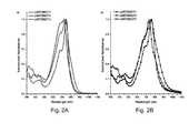
- FIGS. 2A-B compare the UV-Vis-NIR absorption spectra of the three exemplary polymers (A) in solution and (B) in thin film forms.
- FIG. 3 compares the X-ray diffraction patterns of the three exemplary polymers.
- FIG. 4 compares thin film cyclic voltammetry measurements of the three exemplary polymers.
- FIGS. 5A-C show the I D -V G transfer plots of organic field-effect transistor devices incorporating a polymer according to the present teachings as the active channel layer: A) pBBT26BDT1, B) pBBT26BDT2 and C) pBBT26BDT3.
- FIGS. 6A-B show (A) the current density-voltage (J-V) curves and (B) the external quantum efficiency (EQE) spectra of organic bulk-heterojunction photovoltaic devices having a blend photoactive layer that includes a polymer according to the present teachings as the donor material and PC71BM as the acceptor material.
- J-V current density-voltage
- EQE external quantum efficiency
- FIG. 7 shows the device architecture used to investigate the present polymers as hole-transporting materials in perovskite solar cells.
- FIG. 8 compares the current density-voltage (J-V) curves of perovskite photovoltaic devices having a hole-transport layer composed of (i) doped spiro-OMeTAD, (ii) undoped spiro-OMeTAD, (iii) pBBT26BDT1, (iv) pBBT26BDT2 and (v) pBBT26BDT3.
- compositions are described as having, including, or comprising specific components, or where processes are described as having, including, or comprising specific process steps, it is contemplated that compositions of the present teachings also consist essentially of, or consist of, the recited components, and that the processes of the present teachings also consist essentially of, or consist of, the recited process steps.
- a “p-type semiconductor material” or a “donor” material refers to a semiconductor material, for example, an organic semiconductor material, having holes as the majority current or charge carriers.
- a p-type semiconductor material when deposited on a substrate, it can provide a hole mobility in excess of about 10 ⁇ 5 cm 2 /Vs.
- a p-type semiconductor In the case of field-effect devices, a p-type semiconductor also can exhibit a current on/off ratio of greater than about 10.
- an “n-type semiconductor material” or an “acceptor” material refers to a semiconductor material, for example, an organic semiconductor material, having electrons as the majority current or charge carriers.
- an n-type semiconductor material when deposited on a substrate, it can provide an electron mobility in excess of about 10 ⁇ 5 cm 2 /Vs. In the case of field-effect devices, an n-type semiconductor also can exhibit a current on/off ratio of greater than about 10.
- mobility refers to a measure of the velocity with which charge carriers, for example, holes (or units of positive charge) in the case of a p-type semiconductor material and electrons (or units of negative charge) in the case of an n-type semiconductor material, move through the material under the influence of an electric field.
- charge carriers for example, holes (or units of positive charge) in the case of a p-type semiconductor material and electrons (or units of negative charge) in the case of an n-type semiconductor material. This parameter, which depends on the device architecture, can be measured using a field-effect device or space-charge limited current measurements.
- fill factor is the ratio (given as a percentage) of the actual maximum obtainable power, (P m or V mp *J mp ), to the theoretical (not actually obtainable) power, (J sc *V oc ). Accordingly, FF can be determined using the equation: FF ( V mp *J mp )/( J sc *V oc ) where J mp and V mp represent the current density and voltage at the maximum power point (P m ), respectively, this point being obtained by varying the resistance in the circuit until J*V is at its greatest value; and J sc and V oc represent the short circuit current and the open circuit voltage, respectively.
- Fill factor is a key parameter in evaluating the performance of solar cells. Commercial solar cells typically have a fill factor of about 0.60% or greater.
- V oc the open-circuit voltage
- the power conversion efficiency (PCE) of a solar cell is the percentage of power converted from absorbed light to electrical energy.
- the PCE of a solar cell can be calculated by dividing the maximum power point (P m ) by the input light irradiance (E, in W/m 2 ) under standard test conditions (STC) and the surface area of the solar cell (A c in m 2 ).
- STC typically refers to a temperature of 25° C. and an irradiance of 1000 W/m 2 with an air mass 1.5 (AM 1.5) spectrum.
- a component such as a thin film layer
- a component can be considered “photoactive” if it contains one or more compounds that can absorb photons to produce excitons for the generation of a photocurrent.
- solution-processable refers to compounds (e.g., polymers), materials, or compositions that can be used in various solution-phase processes including spin-coating, printing (e.g., inkjet printing, gravure printing, offset printing and the like), spray coating, electrospray coating, drop casting, dip coating, and blade coating.
- a “polymeric compound” refers to a molecule including a plurality of one or more repeating units connected by covalent chemical bonds.
- a polymeric compound can be represented by the general formula: * M * wherein M is the repeating unit or monomer.
- the polymeric compound can have only one type of repeating unit as well as two or more types of different repeating units. When a polymeric compound has only one type of repeating unit, it can be referred to as a homopolymer. When a polymeric compound has two or more types of different repeating units, the term “copolymer” or “copolymeric compound” can be used instead.
- a copolymeric compound can include repeating units * M a * and * M b * where M a and M b represent two different repeating units.
- the assembly of the repeating units in the copolymer can be head-to-tail, head-to-head, or tail-to-tail.
- the copolymer can be a random copolymer, an alternating copolymer, or a block copolymer.
- the general formula: * M a x -M b y * can be used to represent a copolymer of M a and M b having x mole fraction of M a and y mole fraction of M b in the copolymer, where the manner in which comonomers M a and M b is repeated can be alternating, random, regiorandom, regioregular, or in blocks.
- a polymeric compound can be further characterized by its degree of polymerization (n) and molar mass (e.g., number average molecular weight (M n ) and/or weight average molecular weight (M w ) depending on the measuring technique(s)).
- halo or “halogen” refers to fluoro, chloro, bromo, and iodo.
- alkyl refers to a straight-chain or branched saturated hydrocarbon group.
- alkyl groups include methyl (Me), ethyl (Et), propyl (e.g., n-propyl and iso-propyl), butyl (e.g., n-butyl, iso-butyl, sec-butyl, tert-butyl), pentyl groups (e.g., n-pentyl, iso-pentyl, neo-pentyl), hexyl groups, and the like.
- an alkyl group can have 1 to 40 carbon atoms (i.e., C 1-40 alkyl group), for example, 1-20 carbon atoms (i.e., C 1-20 alkyl group).
- an alkyl group can have 1 to 6 carbon atoms, and can be referred to as a “lower alkyl group.” Examples of lower alkyl groups include methyl, ethyl, propyl (e.g., n-propyl and iso-propyl), and butyl groups (e.g., n-butyl, iso-butyl, sec-butyl, tert-butyl).
- alkyl groups can be substituted as described herein.
- An alkyl group is generally not substituted with another alkyl group, an alkenyl group, or an alkynyl group.
- haloalkyl refers to an alkyl group having one or more halogen substituents.
- a haloalkyl group can have 1 to 40 carbon atoms (i.e., C 1-40 haloalkyl group), for example, 1 to 20 carbon atoms (i.e., C 1-20 haloalkyl group).
- Examples of haloalkyl groups include CF 3 , C 2 F 5 , CHF 2 , CH 2 F, CCl 3 , CHCl 2 , CH 2 Cl, C 2 Cl 5 , and the like.
- Perhaloalkyl groups i.e., alkyl groups where all of the hydrogen atoms are replaced with halogen atoms (e.g., CF 3 and C 2 F 5 ), are included within the definition of “haloalkyl.”
- a C 1-40 haloalkyl group can have the formula —C s H 2s+1 ⁇ t X 0 t , where X 0 , at each occurrence, is F, Cl, Br or I, s is an integer in the range of 1 to 40, and t is an integer in the range of 1 to 81, provided that t is less than or equal to 2s+1.
- Haloalkyl groups that are not perhaloalkyl groups can be substituted as described herein.
- alkoxy refers to —O-alkyl group.
- alkoxy groups include, but are not limited to, methoxy, ethoxy, propoxy (e.g., n-propoxy and isopropoxy), t-butoxy, pentoxyl, hexoxyl groups, and the like.
- the alkyl group in the —O-alkyl group can be substituted as described herein.
- alkylthio refers to an —S— alkyl group.
- alkylthio groups include, but are not limited to, methylthio, ethylthio, propylthio (e.g., n-propylthio and isopropylthio), t-butylthio, pentylthio, hexylthio groups, and the like.
- the alkyl group in the —S-alkyl group can be substituted as described herein.
- alkenyl refers to a straight-chain or branched alkyl group having one or more carbon-carbon double bonds.
- alkenyl groups include ethenyl, propenyl, butenyl, pentenyl, hexenyl, butadienyl, pentadienyl, hexadienyl groups, and the like.
- the one or more carbon-carbon double bonds can be internal (such as in 2-butene) or terminal (such as in 1-butene).
- an alkenyl group can have 2 to 40 carbon atoms (i.e., C 2-40 alkenyl group), for example, 2 to 20 carbon atoms (i.e., C 2-20 alkenyl group).
- alkenyl groups can be substituted as described herein.
- An alkenyl group is generally not substituted with another alkenyl group, an alkyl group, or an alkynyl group.
- alkynyl refers to a straight-chain or branched alkyl group having one or more triple carbon-carbon bonds.
- alkynyl groups include ethynyl, propynyl, butynyl, pentynyl, hexynyl, and the like.
- the one or more triple carbon-carbon bonds can be internal (such as in 2-butyne) or terminal (such as in 1-butyne).
- an alkynyl group can have 2 to 40 carbon atoms (i.e., C 2-40 alkynyl group), for example, 2 to 20 carbon atoms (i.e., C 2-20 alkynyl group).
- alkynyl groups can be substituted as described herein.
- An alkynyl group is generally not substituted with another alkynyl group, an alkyl group, or an alkenyl group.
- a “cyclic moiety” can include one or more (e.g., 1-6) carbocyclic or heterocyclic rings.
- the cyclic moiety can be a cycloalkyl group, a heterocycloalkyl group, an aryl group, or a heteroaryl group (i.e., can include only saturated bonds, or can include one or more unsaturated bonds regardless of aromaticity), each including, for example, 3-24 ring atoms and optionally can be substituted as described herein.
- the “monocyclic moiety” can include a 3-14 membered aromatic or non-aromatic, carbocyclic or heterocyclic ring.
- a monocyclic moiety can include, for example, a phenyl group or a 5- or 6-membered heteroaryl group, each of which optionally can be substituted as described herein.
- the cyclic moiety is a “polycyclic moiety”
- the “polycyclic moiety” can include two or more rings fused to each other (i.e., sharing a common bond) and/or connected to each other via a spiro atom, or one or more bridged atoms.
- a polycyclic moiety can include an 8-24 membered aromatic or non-aromatic, carbocyclic or heterocyclic ring, such as a C 8-24 aryl group or an 8-24 membered heteroaryl group, each of which optionally can be substituted as described herein.
- a “fused ring” or a “fused ring moiety” refers to a polycyclic ring system having at least two rings where at least one of the rings is aromatic and such aromatic ring (carbocyclic or heterocyclic) has a bond in common with at least one other ring that can be aromatic or non-aromatic, and carbocyclic or heterocyclic.
- aromatic ring or heterocyclic
- These polycyclic ring systems can be highly ⁇ -conjugated and optionally substituted as described herein.
- cycloalkyl refers to a non-aromatic carbocyclic group including cyclized alkyl, alkenyl, and alkynyl groups.
- a cycloalkyl group can have 3 to 24 carbon atoms, for example, 3 to 20 carbon atoms (e.g., C 3-14 cycloalkyl group).
- a cycloalkyl group can be monocyclic (e.g., cyclohexyl) or polycyclic (e.g., containing fused, bridged, and/or spiro ring systems), where the carbon atoms are located inside or outside of the ring system.
- cycloalkyl groups include cyclopropyl, cyclobutyl, cyclopentyl, cyclohexyl, cycloheptyl, cyclopentenyl, cyclohexenyl, cyclohexadienyl, cycloheptatrienyl, norbornyl, norpinyl, norcaryl, adamantyl, and spiro[4.5]decanyl groups, as well as their homologs, isomers, and the like.
- cycloalkyl groups can be substituted as described herein.
- heteroatom refers to an atom of any element other than carbon or hydrogen and includes, for example, nitrogen, oxygen, silicon, sulfur, phosphorus, and selenium.
- cycloheteroalkyl refers to a non-aromatic cycloalkyl group that contains at least one ring heteroatom selected from O, S, Se, N, P, and Si (e.g., O, S, and N), and optionally contains one or more double or triple bonds.
- a cycloheteroalkyl group can have 3 to 24 ring atoms, for example, 3 to 20 ring atoms (e.g., 3-14 membered cycloheteroalkyl group).
- N, P, S, or Se atoms in a cycloheteroalkyl ring may be oxidized (e.g., morpholine N-oxide, thiomorpholine S-oxide, thiomorpholine S,S-dioxide).
- nitrogen or phosphorus atoms of cycloheteroalkyl groups can bear a substituent, for example, a hydrogen atom, an alkyl group, or other substituents as described herein.
- Cycloheteroalkyl groups can also contain one or more oxo groups, such as oxopiperidyl, oxooxazolidyl, dioxo-(1H,3H)-pyrimidyl, oxo-2(1H)-pyridyl, and the like.
- oxo groups such as oxopiperidyl, oxooxazolidyl, dioxo-(1H,3H)-pyrimidyl, oxo-2(1H)-pyridyl, and the like.
- cycloheteroalkyl groups include, among others, morpholinyl, thiomorpholinyl, pyranyl, imidazolidinyl, imidazolinyl, oxazolidinyl, pyrazolidinyl, pyrazolinyl, pyrrolidinyl, pyrrolinyl, tetrahydrofuranyl, tetrahydrothiophenyl, piperidinyl, piperazinyl, and the like.
- cycloheteroalkyl groups can be substituted as described herein.
- aryl refers to an aromatic monocyclic hydrocarbon ring system or a polycyclic ring system in which two or more aromatic hydrocarbon rings are fused (i.e., having a bond in common with) together or at least one aromatic monocyclic hydrocarbon ring is fused to one or more cycloalkyl and/or cycloheteroalkyl rings.
- An aryl group can have 6 to 24 carbon atoms in its ring system (e.g., C 6-20 aryl group), which can include multiple fused rings.
- a polycyclic aryl group can have 8 to 24 carbon atoms. Any suitable ring position of the aryl group can be covalently linked to the defined chemical structure.
- aryl groups having only aromatic carbocyclic ring(s) include phenyl, 1-naphthyl (bicyclic), 2-naphthyl (bicyclic), anthracenyl (tricyclic), phenanthrenyl (tricyclic), pentacenyl (pentacyclic), and like groups.
- polycyclic ring systems in which at least one aromatic carbocyclic ring is fused to one or more cycloalkyl and/or cycloheteroalkyl rings include, among others, benzo derivatives of cyclopentane (i.e., an indanyl group, which is a 5,6-bicyclic cycloalkyl/aromatic ring system), cyclohexane (i.e., a tetrahydronaphthyl group, which is a 6,6-bicyclic cycloalkyl/aromatic ring system), imidazoline (i.e., a benzimidazolinyl group, which is a 5,6-bicyclic cycloheteroalkyl/aromatic ring system), and pyran (i.e., a chromenyl group, which is a 6,6-bicyclic cycloheteroalkyl/aromatic ring system).
- aryl groups include benzodioxanyl, benzodioxolyl, chromanyl, indolinyl groups, and the like.
- aryl groups can be substituted as described herein.
- an aryl group can have one or more halogen substituents, and can be referred to as a “haloaryl” group.
- Perhaloaryl groups i.e., aryl groups where all of the hydrogen atoms are replaced with halogen atoms (e.g., —C 6 F 5 ), are included within the definition of “haloaryl.”
- an aryl group is substituted with another aryl group and can be referred to as a biaryl group.
- Each of the aryl groups in the biaryl group can be substituted as disclosed herein.
- arylalkyl refers to an -alkyl-aryl group, where the arylalkyl group is covalently linked to the defined chemical structure via the alkyl group.
- An arylalkyl group is within the definition of a —Y—C 6-14 aryl group, where Y is as defined herein.
- An example of an arylalkyl group is a benzyl group (—CH 2 —C 6 H 5 ).
- An arylalkyl group can be optionally substituted, i.e., the aryl group and/or the alkyl group, can be substituted as disclosed herein.
- heteroaryl refers to an aromatic monocyclic ring system containing at least one ring heteroatom selected from oxygen (O), nitrogen (N), sulfur (S), silicon (Si), and selenium (Se) or a polycyclic ring system where at least one of the rings present in the ring system is aromatic and contains at least one ring heteroatom.
- Polycyclic heteroaryl groups include those having two or more heteroaryl rings fused together, as well as those having at least one monocyclic heteroaryl ring fused to one or more aromatic carbocyclic rings, non-aromatic carbocyclic rings, and/or non-aromatic cycloheteroalkyl rings.
- a heteroaryl group as a whole, can have, for example, 5 to 24 ring atoms and contain 1-5 ring heteroatoms (i.e., 5-20 membered heteroaryl group).
- the heteroaryl group can be attached to the defined chemical structure at any heteroatom or carbon atom that results in a stable structure.
- heteroaryl rings do not contain O—O, S—S, or S—O bonds.
- one or more N or S atoms in a heteroaryl group can be oxidized (e.g., pyridine N-oxide, thiophene S-oxide, thiophene S,S-dioxide).
- heteroaryl groups include, for example, the 5- or 6-membered monocyclic and 5-6 bicyclic ring systems shown below:
- T is O, S, NH, N-alkyl, N-aryl, N-(arylalkyl) (e.g., N-benzyl), SiH 2 , SiH(alkyl), Si(alkyl) 2 , SiH(arylalkyl), Si(arylalkyl) 2 , or Si(alkyl)(arylalkyl).
- N-alkyl N-aryl, N-(arylalkyl) (e.g., N-benzyl)
- SiH 2 SiH(alkyl), Si(alkyl) 2 , SiH(arylalkyl), Si(arylalkyl) 2 , or Si(alkyl)(arylalkyl).
- heteroaryl rings examples include pyrrolyl, furyl, thienyl, pyridyl, pyrimidyl, pyridazinyl, pyrazinyl, triazolyl, tetrazolyl, pyrazolyl, imidazolyl, isothiazolyl, thiazolyl, thiadiazolyl, isoxazolyl, oxazolyl, oxadiazolyl, indolyl, isoindolyl, benzofuryl, benzothienyl, quinolyl, 2-methylquinolyl, isoquinolyl, quinoxalyl, quinazolyl, benzotriazolyl, benzimidazolyl, benzothiazolyl, benzisothiazolyl, benzisoxazolyl, benzoxadiazolyl, benzoxazolyl, cinnolinyl, 1H-indazolyl, 2H-indazolyl
- heteroaryl groups include 4,5,6,7-tetrahydroindolyl, tetrahydroquinolinyl, benzothienopyridinyl, benzofuropyridinyl groups, and the like. In some embodiments, heteroaryl groups can be substituted as described herein.
- compounds of the present teachings can include a “divalent group” defined herein as a linking group capable of forming a covalent bond with two other moieties.
- compounds of the present teachings can include a divalent C 1-20 alkyl group (e.g., a methylene group), a divalent C 2-20 alkenyl group (e.g., a vinylyl group), a divalent C 2-20 alkynyl group (e.g., an ethynylyl group).
- a divalent C 6-14 aryl group e.g., a phenylyl group
- a divalent 3-14 membered cycloheteroalkyl group e.g., a pyrrolidylyl
- a divalent 5-14 membered heteroaryl group e.g., a thienylyl group
- a chemical group e.g., —Ar—
- —Ar— is understood to be divalent by the inclusion of the two bonds before and after the group.
- C 1-6 alkyl is specifically intended to individually disclose C 1 , C 2 , C 3 , C 4 , C 5 , C 6 , C 1 -C 6 , C 1 -C 5 , C 1 -C 4 , C 1 -C 3 , C 1 -C 2 , C 2 -C 6 , C 2 -C 5 , C 2 -C 4 , C 2 -C 3 , C 3 -C 6 , C 3 -C 5 , C 3 -C 4 , C 4 -C 6 , C 4 -C 5 , and C 5 -C 6 alkyl.
- an integer in the range of 0 to 40 is specifically intended to individually disclose 0, 1, 2, 3, 4, 5, 6, 7, 8, 9, 10, 11, 12, 13, 14, 15, 16, 17, 18, 19, 20, 21, 22, 23, 24, 25, 26, 27, 28, 29, 30, 31, 32, 33, 34, 35, 36, 37, 38, 39, and 40, and an integer in the range of 1 to 20 is specifically intended to individually disclose 1, 2, 3, 4, 5, 6, 7, 8, 9, 10, 11, 12, 13, 14, 15, 16, 17, 18, 19, and 20.
- phrases “optionally substituted with 1-5 substituents” is specifically intended to individually disclose a chemical group that can include 0, 1, 2, 3, 4, 5, 0-5, 0-4, 0-3, 0-2, 0-1, 1-5, 1-4, 1-3, 1-2, 2-5, 2-4, 2-3, 3-5, 3-4, and 4-5 substituents.
- the present teachings provide novel polymers based on a first repeating unit comprising a benzo[1,2-d;4,5-d′]bistriazole (BBT) moiety and a second repeating unit comprising a benzo[1,2-b:4,5-b′]dithiophene (BDT) moiety.
- BBT benzo[1,2-d;4,5-d′]bistriazole
- BDT benzo[1,2-b:4,5-b′]dithiophene
- BDT benzo[1,2-b:4,5-b′]dithiophene
- each R′ can be H or a substituent.
- Polymers according to the present teachings can have a molecular weight between about 10,000 g/mol and about 150,000 g/mol, and can have a bandgap between about 1.0 and about 2.0.
- the present polymers can include a repeating unit represented by formula (I):
- R 1 at each occurrence, independently is a solubilizing group
- R 2 at each occurrence, independently is selected from the group consisting of H, F, Cl, CN, and a C 1-40 alkyl or haloalkyl group
- R 3 and R 4 at each occurrence, independently are selected from the group consisting of H, F, Cl, and -L-(Ar) m -L′-R 5 ; wherein L and L′, independently are selected from the group consisting of —O—, —S—, —Se—, —C(O)—, —OC(O)—, —C(O)O—, a divalent C 1-40 alkyl or haloalkyl group, and a covalent bond; R 5 is a solubilizing group; Ar, at each occurrence, independently is a C 6-14 aryl group or a 5-14 membered heteroaryl group, each of which optionally is substituted with 1-4 -L′-
- Substitution of alkyl chains (or similar groups such as alkenyl groups, haloalkyl groups, arylalkyl groups, heteroarylalkyl groups and so forth) on the benzo[1,2-d;4,5-d′]bistriazole (BBT) moiety and/or the benzo[1,2-b:4,5-b′]dithiophene (BDT) moiety can improve the solubility of the polymer in various organic solvents, hence improving the processability of the polymer into thin film materials.
- R 1 , R 3 and/or R 4 can be selected from various organic functional groups comprising one or more alkyl, alkenyl, and/or haloalkyl groups, preferably alkyl, alkenyl, and haloalkyl groups having at least 3 carbon atoms.
- R 1 can be a linear or branched C 3-40 alkyl group, while R 2 , at each occurrence, independently can be H or a linear or branched C 3-40 alkyl group.
- R 3 can be -L-(Ar)m-L′-R 5 while R 4 can be H, F, or Cl.
- the present polymer can include a repeating unit represented by formula (II):
- R 1 is a C 3-40 alkyl group
- R 3 is -L-(Ar) m -L′-R 5 , where L, L′, Ar, R 5 , and m are as defined herein.
- R 3 can be an —O—C 3-40 alkyl group.
- R 3 can be a C 3-40 alkyl group.
- R 3 can be —(Ar) m -L′-R 5 , where Ar can be a thienyl or phenyl group, L′ can be O or a covalent bond, and R 5 can be a C 3-40 alkyl group.
- R 3 can be a thienyl group substituted with a C 3-40 alkyl group.
- Polymers of the present teachings and monomers leading to the present polymers can be prepared according to procedures analogous to those described in the Examples.
- Stille coupling or Suzuki coupling reactions can be used to prepare co-polymeric compounds according to the present teachings with high molecular weights and in high yields and purity, as confirmed by 1 H NMR spectra, elemental analysis, and/or GPC measurements.
- the present compounds can be prepared from commercially available starting materials, compounds known in the literature, or via other readily prepared intermediates, by employing standard synthetic methods and procedures known to those skilled in the art.
- Standard synthetic methods and procedures for the preparation of organic molecules and functional group transformations and manipulations can be readily obtained from the relevant scientific literature or from standard textbooks in the field. It will be appreciated that where typical or preferred process conditions (i.e., reaction temperatures, times, mole ratios of reactants, solvents, pressures, etc.) are given, other process conditions can also be used unless otherwise stated.
- Optimum reaction conditions can vary with the particular reactants or solvent used, but such conditions can be determined by one skilled in the art by routine optimization procedures. Those skilled in the art of organic synthesis will recognize that the nature and order of the synthetic steps presented can be varied for the purpose of optimizing the formation of the compounds described herein.
- product formation can be monitored by spectroscopic means, such as nuclear magnetic resonance spectroscopy (NMR, e.g., 1 H or 13 C), infrared spectroscopy (IR), optical absorption/emission spectroscopy (e.g., UV-visible), mass spectrometry (MS), or by chromatography such as high pressure liquid chromatography (HPLC), gas chromatography (GC), gel-permeation chromatography (GPC), or thin layer chromatography (TLC).
- NMR nuclear magnetic resonance spectroscopy
- IR infrared spectroscopy
- IR optical absorption/emission spectroscopy
- MS mass spectrometry
- chromatography such as high pressure liquid chromatography (HPLC), gas chromatography (GC), gel-permeation chromatography (GPC), or thin layer chromatography (TLC).
- HPLC high pressure liquid chromatography
- GC gas chromatography
- GPC gel-permeation chromatography
- TLC thin layer chromatography
- Suitable solvents typically are substantially nonreactive with the reactants, intermediates, and/or products at the temperatures at which the reactions are carried out, i.e., temperatures that can range from the solvent's freezing temperature to the solvent's boiling temperature.
- a given reaction can be carried out in one solvent or a mixture of more than one solvent.
- suitable solvents for a particular reaction step can be selected.
- the present polymers can be ambient-stable, which allows the present polymers to be used in devices intended to be operated in air.
- a compound can be considered “ambient stable” or “stable at ambient conditions” when a device (e.g., an optoelectronic device) incorporating the compound as one of its electronic, optical, or optoelectronic components exhibits a device performance parameter (e.g., carrier mobility, optical absorption) that remains stable (e.g., exhibiting a variance no more than 20%, preferably no more than 10%, from its initial value) after exposure to ambient conditions (including, air, humidity and temperature) over a 3 day, 5 day, or 10-day period.
- a device performance parameter e.g., carrier mobility, optical absorption
- the present polymers also can have good solubility in various common organic solvents.
- a compound can be considered soluble in a solvent when at least 0.1 mg of the compound can be dissolved in 1 mL of the solvent.
- common organic solvents include petroleum ethers; acetonitrile; aromatic hydrocarbons such as benzene, toluene, xylene, and mesitylene; ketones such as acetone, and methyl ethyl ketone; ethers such as tetrahydrofuran, dioxane, bis(2-methoxyethyl) ether, diethyl ether, di-isopropyl ether, and t-butyl methyl ether; alcohols such as methanol, ethanol, butanol, and isopropyl alcohol; aliphatic hydrocarbons such as hexanes; esters such as methyl acetate, ethyl acetate, methyl formate, ethyl
- the present polymers can be fabricated into various articles of manufacture using solution processing techniques in addition to other more expensive processes such as vapor deposition.
- Various solution processing techniques have been used with organic electronics.
- Common solution processing techniques include, for example, spin coating, slot coating, drop-casting, zone casting, dip coating, blade coating, or spraying.
- Another example of solution processing technique is printing.
- “printing” includes a noncontact process such as inkjet printing, microdispensing and the like, and a contact process such as screen-printing, gravure printing, offset printing, flexographic printing, lithographic printing, pad printing, microcontact printing and the like.
- Polymers of the present teachings can exhibit semiconductor behavior such as optimized light absorption/charge separation in a photovoltaic device; charge transport/recombination/light emission in a light-emitting device; and/or high carrier mobility and/or good current modulation characteristics in a field-effect device.
- the present polymers can possess certain processing advantages such as solution-processability and/or good stability (e.g., air stability) in ambient conditions.
- the polymers of the present teachings can be used to prepare p-type (donor or hole-transporting) semiconductor materials, which in turn can be used alone or together with other p-type, n-type (acceptor or electron-transporting), and/or ambipolar semiconductor materials to fabricate various organic or hybrid optoelectronic articles, structures and devices.
- Various articles of manufacture including optical devices, optoelectronic devices, and electronic devices such as thin film semiconductors, organic and hybrid photovoltaic devices, photodetectors, thin film transistors such as organic field-effect transistors (OFETs), and organic light-emitting devices such as organic light-emitting diodes (OLEDs) and organic light emitting transistors (OLETs), that make use of the polymers disclosed herein are within the scope of the present teachings as are methods of making the same.
- the present polymers can offer processing and operation advantages in the fabrication and/or the use of these devices.
- articles of manufacture such as the various devices described herein can be an optical or optoelectronic device including a first electrode, a second electrode, and a semiconducting component disposed between the first electrode and the second electrode, where the semiconducting component includes a polymer of the present teachings.
- the present teachings relate to an organic field effect transistor (OFET) that incorporates a semiconductor material comprising a polymer according to the present teachings.
- the OFET can include a substrate, a gate electrode, a gate dielectric, source and drain electrodes, and a thin film semiconductor comprising the present polymer, where the thin film semiconductor is in contact with the source and drain electrodes on one side, and the gate dielectric on another side.
- the OFET can have a device architecture selected from (a) bottom-gate top-contact structure, (b) bottom-gate bottom-contact structure, (c) top-gate bottom-contact structure, and (d) top-gate top-contact structure.
- the OFETs can be fabricated on doped silicon substrates or plastic foils, and the gate dielectric can be composed of inorganic, organic, or hybrid materials as known by those skilled in the art.
- Gate and source/drain contacts can be made of Au, other metals, or conducting polymers and deposited by vapor-deposition and/or printing.
- the present teachings relate to an organic photovoltaic device (OPV) or organic solar cell, in particular, a bulk heterojunction solar cell.
- OCV organic photovoltaic device
- Polymers of the present teachings can exhibit broad optical absorption and/or a tuned redox properties and bulk carrier mobilities, making them desirable for such applications.
- the bulk heterojunction solar cells can include an anode, a cathode, a photoactive layer in between the anode and the cathode, and one or more interlayers.
- the photoactive layer can incorporate a blend material (e.g., a blended film) including a polymer of the present teachings as the donor material and an acceptor material.
- Typical acceptor materials include fullerene-based compounds such as [6,6]-phenyl-C 61 -butyric acid methyl ester (PC61BM) or [6,6]-phenyl-C 71 -butyric acid methyl ester (PC71BM).
- PC61BM fullerene-based compounds
- PC71BM [6,6]-phenyl-C 71 -butyric acid methyl ester
- Other acceptor materials that can be used include n-type small molecule or polymeric semiconductors known in the art.
- the present polymers exhibit good hole-transporting properties which allow them to be used as p-type semiconductors in optoelectronic devices such as organic field-effect transistors (OFET) and organic photovoltaic (OPV) devices
- OFET organic field-effect transistors
- OOV organic photovoltaic
- the present polymers in pristine form (i.e., without doping) can lead to exceptional power conversion efficiencies.
- hybrid organic-inorganic perovskite solar cells using the present polymers alone (i.e., without addition of any chemical dopants) as the hole-transport layer can have power conversion efficiencies (PCE) as high as 14.5%.
- an aspect of the present teachings relates to hybrid organic-inorganic perovskite photovoltaic device including a hole-transporting material comprising a polymer described herein.
- the device generally includes a first electrode, a second electrode, a light-absorbing layer between the first and second electrodes that comprises a perovskite compound and is in contact with the hole-transporting material.
- An optional blocking layer also can be present, for example, adjacent to either the first electrode or the second electrode.
- the hybrid organic-inorganic perovskite photovoltaic device can have a mesostructured device structure.
- the perovskite absorber can be infiltrated within a mesoporous metal oxide scaffold (which can be an electron-transporting oxide such as TiO 2 , ZnO, or an insulating layer such as Al 2 O 3 , ZrO 2 ) formed on top of a compact ZnO or TiO 2 blocking layer, which itself can be deposited on a transparent conducting oxide substrate (e.g., FTO) that functions as the anode.
- a hole-transporting material comprising a polymer described herein can be deposited in contact with the perovskite layer.
- a high work-function metal electrode e.g., Ag or Au
- the hybrid organic-inorganic perovskite photovoltaic device can have a planar device structure.
- the planar device can include, from bottom to top, the substrate, a transparent conducting oxide (e.g., FTO) as the anode, an optional electron-transport layer (ETL) comprising an electron-transporting (n-type semiconducting) material, the perovskite layer, a hole-transport layer comprising a hole-transporting (p-type semiconducting) material which includes a polymer described herein, and a metal electrode as the cathode.
- FTO transparent conducting oxide
- ETL electron-transport layer
- p-type semiconducting hole-transporting
- a blocking layer composed of a compact TiO 2 or ZnO film can be deposited on the anode substrate to improve the morphology of the overlying perovskite.
- the planar device can have an inverted structure and can include, from bottom to top, the substrate, a transparent conducting oxide (e.g., FTO) as the cathode, a hole-transport layer comprising a hole-transporting (p-type semiconducting) material which includes a polymer described herein, the perovskite layer, an optional electron-transport layer (ETL) comprising an electron-transporting (n-type semiconducting) material, and a metal electrode as the anode.
- the ETL for example, can be composed of one or more fullerene compounds such as PC61BM and PC71BM.
- a hole-blocking layer e.g., bathocuproine, BCP
- BCP bathocuproine
- the perovskite photovoltaic device can be provided on a substrate which can be a solid, rigid or flexible layer designed to provide robustness.
- the substrate can be transparent or semi-transparent in the spectral region of interest.
- a material is considered “transparent” when it has transmittance over 50%, and a material is considered “semi-transparent” when it has transmittance between about 50% and about 5%.
- the substrate can comprise any suitable material known in the art such as glass or a flexible plastic (polymer) film. Examples of suitable plastic substrates include, but are not limited to, polyethylene terephthalate (PET), polyimide, and polyethylene naphthalate (PEN).
- the first and second electrodes can be selected from various materials of different work functions.
- a transparent first electrode is provided on the substrate, where the transparent electrode is made of a transparent conducting oxide (TCO) such as indium tin oxide (ITO) and fluorine-doped tin oxide (FTO).
- TCO transparent conducting oxide
- ITO indium tin oxide
- FTO fluorine-doped tin oxide
- the first electrode/substrate composite can be selected from FTO-coated glass, ITO-coated glass, ITO-coated PET, and FTO-coated PET.
- the second electrode typically is a metal electrode selected from gold, silver, and aluminum.
- the light-absorbing layer is composed of a perovskite structured compound; most commonly, a hybrid organic-inorganic lead or tin halide ABX 3 , where A is an organic cation [typically CH 3 NH 3 + (methylammonium or MA) or HN ⁇ CHNH 3 + (formamidinium or FA)], B is Sn 2+ or Pb 2+ , and X is a halide anion that bonds to both.
- methylammonium lead trihalide CH 3 NH 3 PbX 3 , or MAPbX 3 where X is a halogen ion such as I ⁇ , Br ⁇ , or Cl ⁇
- A is an organic cation [typically CH 3 NH 3 + (methylammonium or MA) or HN ⁇ CHNH 3 + (formamidinium or FA)]
- B is Sn 2+ or Pb 2+
- X is a halide anion that bonds to both.
- methylammonium lead trihalide
- the light-absorbing layer can comprise the perovskite compound MAPBI 3 or MAPbI 3-x Cl x , where x is 1 or 2.
- the light-absorbing layer can have a thickness between about 20 nm and about 800 nm.
- the morphology and the crystal structure of the perovskite absorbers can significantly affect the performance of the photovoltaic device.
- Different deposition methods have been developed in attempt to improve the resulting perovskite structure.
- the major solution-based deposition methods include one-step precursor deposition, sequential deposition, two-step spin-coating deposition, and spray-coating deposition.
- a precursor solution containing both the metal precursor (e.g., PbX 2 ) and the organic precursor (e.g., MAX) in a solvent such as ⁇ -butyrolacetone (GBL) and N,N-dimethylformamide (DMF) is deposited in one-step, using spin-coating or spray-coating, respectively.
- a precursor solution containing only the metal precursor e.g., PbI 2
- a precursor solution containing only the organic precursor e.g., MAI
- a thermal annealing step e.g., at ⁇ 100° C.
- Vapor-phase deposition methods also have been used. These include dual source vacuum deposition and sequential vapor deposition. In these deposition processes, instead of depositing the precursors in solution-phase, the metal precursor and the organic precursor are evaporated either simultaneously from separate sources or sequentially layer by layer. In vapor-assisted solution process, the metal precursor solution is first spin-coated onto the substrate. Then, the precursor-coated substrate is annealed in a vapor containing the organic precursor to yield the perovskite film.
- the metal precursor solution is first spin-coated onto the substrate. Then, the precursor-coated substrate is annealed in a vapor containing the organic precursor to yield the perovskite film.
- the perovskite solar cells includes a hole-transporting material consisting of a pristine polymer, specifically, a copolymer including a benzo[1,2-d;4,5-d′]bistriazole-containing repeating unit and a benzo[1,2-b:4,5-b′]dithiophene-containing repeating unit.
- the hole-transporting material is free of any dopants typically used with spiro-OMeTAD, the state-of-the-art HTM compound, such as 4-tert-butylpyridine (TBP), bis(trifluoromethane)sulfonimide lithium salt (Li-TFSI), and tris(2-(1H-pyrazol-1-yl)4-tert-butylpyridine)cobalt(III) tris(bis(trifluoromethylsulfonyl)imide) (FK209).
- TBP 4-tert-butylpyridine
- Li-TFSI bis(trifluoromethane)sulfonimide lithium salt
- FK209 tris(2-(1H-pyrazol-1-yl)4-tert-butylpyridine)cobalt(III) tris(bis(trifluoromethylsulfonyl)imide)
- the pervoskite photovoltaic device can include one or more optional interface layers (“interlayers”) between the anode and the light-absorbing layer and/or between the cathode and the light-absorbing layer.
- an optional smoothing layer e.g., a film of 3,4-polyethylenedioxythiophene (PEDOT), or 3,4-polyethylenedioxythiophene:polystyrene-sulfonate (PEDOT:PSS)
- PEDOT 3,4-polyethylenedioxythiophene
- PSS 3,4-polyethylenedioxythiophene:polystyrene-sulfonate
- the optional interlayer(s) can perform other functions such as reducing the energy barrier between the light-absorbing layer and the electrode, forming selective contacts for a single type of carrier (e.g., a hole-blocking layer), modifying the work function of the adjacent electrode, and/or protecting the underlying light-absorbing layer.
- a transition metal oxide layer such as V 2 O 5 , MoO 3 , WO 3 and NiO can be used as the p-type buffer.
- an n-type buffer composed of LiF, CsF or similar fluorides can be provided.
- the interlayers can be solution-processed (e.g., sol-gel deposition, self-assembled monolayers) or deposited by vacuum processes such as thermal evaporation or sputtering.
- tetraaminobenzene tetrahydrobromide (TAB.4HBr, 21 g, 45.5 mmol) was added to 48% aqueous HBr (300 mL) and allowed to cool down to 0° C.
- Sodium nitrite NaNO 3 , 31.38 g, 454.7 mmol was dissolved in deionized water (500 mL) and was added dropwise to the reaction mixture using an additional funnel in air. Brown gas evolved upon addition of the NaNO 3 solution. After addition of the NaNO 3 solution, the reaction was allowed to warm up to room temperature overnight. The reaction mixture was heated to 100° C.
- the crude Br 2 -BBT was used for the next step without further purification. Specifically, the crude Br 2 -BBT was added to DMF (90 mL) together with anhydrous K 2 CO 3 (15.06 g, 109.0 mmol), 1-bromohexane (14.04 mL, 100.0 mmol) and the reaction mixture was allowed to stir at room temperature for 3 days under a nitrogen environment. The reaction mixture was added to 500 mL of water and extracted using dichloromethane.
- the residue was dry loaded into a silica column with hexane as the eluent to separate the resulting Stille coupled isomers, giving an overall yield of ⁇ 70%.
- the isomer Th 2 -BBT26 was obtained at a yield of 19% (4.2 g) as red crystalline solids.
- Th 2 -BBT based polymers The 2,6-dialkylated isomer Th 2 -BBT26 (1.00 g, 2.03 mmol) was dissolved in chloroform and placed in an ice bath. To the solution was added dropwise NBS (0.722 g, 4.06 mmol) dissolved in chloroform (200 mL). After addition of NBS, the reaction was allowed to warm up to room temperature overnight. The reaction was quenched using aqueous sodium thiosulfate (Na 2 S 2 O 3 ) and the organic layer was collected, dried over anhydrous MgSO 4 and filtered.
- NBS 0.722 g, 4.06 mmol
- the dibromo compound was reacted with distannylated benzo[1,2-b:4,5-b′]dithiophenes (BDTs) to give Th 2 -BBT-co-BDT polymers.
- BDTs distannylated benzo[1,2-b:4,5-b′]dithiophenes
- (BrTh) 2 -BBT26 (128 mg, 0.20 mmol) and 1 equivalence of the distannyl BDT monomer (0.20 mmol) was added Pd(PPh 3 ) 4 (9 mg, 4 mol %) in a round-bottom flask purged with nitrogen.
- 20 mL of dry toluene and 7 mL of dry DMF were injected into the flask and the reaction was stirred at 100° C. for 1 day.
- the reaction mixture was allowed to cool to room temperature and was poured into 200 mL of methanol. The mixture was stirred for 3 h at room temperature and then filtered. The resulting crude polymer was purified using Soxhlet extraction with acetone, hexanes and finally, chloroform.
- pBBT26BDT2 Blue solids (90% yield). Anal. Calcd. for (C 80 H 108 N 6 O 2 S 6 ) n : C, 73.12; H, 8.28; N, 6.40; 0, 2.44; S, 9.76. Found: C, 73.45; H, 8.34; N, 6.49. GPC in trichlorobenzene, 150° C.: Mw: 118977, PDI: 2.13.
- Th 2 -BBT-co-BDT polymers from Example 1 were characterized via UV-Vis-NIR spectroscopy, X-ray diffraction studies, and cyclic voltammetry experiments. Relevant chemical and physical data are reported in Table 1.
- the optical absorption spectra of the Th 2 -BBT-co-BDT polymers were recorded both in chloroform and as spin-coated films ( FIG. 2 ). All three polymers exhibit rather low bandgaps, with values of ⁇ 1.3 eV in thin films and ⁇ 1.4 eV in solution.
- Th 2 -BBT-co-BDT polymers are largely amorphous due to the lack of strong diffraction peaks ( FIG. 3 ).
- OFET organic field-effect transistor
- OTS n-octadecyltrichlorosilane
- Th 2 -BBT-co-BDT polymers as the active semiconductor layer.
- OTS n-octadecyltrichlorosilane
- the 300 nm Si/SiO 2 substrates were cleaned first in an ultrasonic bath of isopropyl alcohol followed by O 2 plasma treatment.
- the substrates were then immersed in the OTS-hexane solution for an hour and subsequently sonicated with hexane and dried by N 2 flow.
- the polymer solutions in chlorobenzene (20 mg/ml) were spin-coated on the substrates.
- FIG. 5 provides the I D -V G transfer plots of sample OFET devices.
- the Th 2 .BBT-co-BDT polymers displayed average hole mobilities ( ⁇ hole ) in the order of 10 ⁇ 2 -10 ⁇ 3 V ⁇ cm ⁇ 1 s ⁇ 1 with on/off ratio in the order of 10 2 -10 4 . No n-type mobility was observed.
- FIG. 6 provides the current density-voltage (J-V) curves and EQE spectra of sample OPV devices.
- Table 2 summarizes the key device parameters for the OFET and OPV devices.
- Perovskite solar cells using the present polymers in pristine form (without dopants) as hole-transport layer (HTL) were fabricated.
- a simplified PHJSC architecture was used with the device geometry being FTO/TiO 2 /CH 3 NH 3 PbCl 3-x I x /HTL/Au ( FIG. 7 ).
- the mixed-halide perovskite absorber of ⁇ 300 nm was prepared on planar TiO 2 /FTO substrates.
- Control devices were fabricated with 2,2′,7,7′-tetrakis-(N,N-di-4-methoxyphenylamino)-9,9′-spirobifluorene (spiro-OMeTAD) as the HTL with and without the dopant lithium-bis(trifluoromethanesulfonyl)imide (Li-TFSI).
- spiro-OMeTAD 2,2′,7,7′-tetrakis-(N,N-di-4-methoxyphenylamino)-9,9′-spirobifluorene
- Li-TFSI lithium-bis(trifluoromethanesulfonyl)imide
- fluorine-doped tin oxide (FTO) glass substrates were ultrasonically cleaned in detergent, methanol, isopropanol sequentially followed by plasma treatment for 15 minutes.
- FTO fluorine-doped tin oxide
- a 0.013 HCl solution (2.53 mL of anhydrous ethanol and 35 ⁇ L of 2 M HCl) was added drop-wise under vigorous stirring into titanium isopropoxide solution (375 uL titanium tetraisopropoxide in 2.53 mL anhydrous ethanol).
- a 50 nm TiO 2 compact layer was deposited on FTO substrates by spin coating the sol-gel solution at 1000 rpm for 40 s. After spin coating, the substrates were sintered at 500° C. for 30 minutes.
- the FTO/TiO 2 substrates were transferred into a humidity box with relative humidity around 3% for spin coating the perovskite layer at 2000 rpm for 40 s.
- the as-casted perovskite layer was thermal annealed at 100° C. for 1 hour for crystallization.
- the spin-coating of hole transporting materials was performed at 2000 rpm for 40 s in glove box using polymer solution in chlorobenzene (10 mg/mL).
- the spiro-OMeTAD solution 80 mg spiro-OMeTAD, 28.5 ml 4-tertbutylpyridine and 17.5 ml lithium-bis(trifluoromethanesulfonyl)imide solution (520 mg/ml in acetonitrile) all dissolved in 1 ml chlorobenzene) was spin-coated at 4,000 r.p.m. for 30 s.
- the devices were completed by thermal evaporating 100 nm gold electrode with an active area of 0.09 cm 2 .
- the solar cell devices were tested in air with shadow mask of 0.12 cm 2 under A.M. 1.5 radiation (100 mW/cm 2 ) using a solar simulator source (Newport Inc.) and Keithley 2400 source meter.
- the EQE spectrum was characterized by an Oriel model QE-PV-SI instrument equipped with a NIST-certified Si diode.
- Molar UV-Vis absorption spectra were recorded on a Lambda 900 Spectrometer from Perkin Elmer.
- Polymer UV-Vis-NIR absorption spectra were recorded on a Perkin Elmer LAMBDA 1050, with a 150 mm integrating sphere for thin film measurements.
- the cross-sectional TEM sample was prepared by standard focused ion beam (FIB) milling and lift off processes using an FEI Helios Nanolab Dual Beam scanning electron and focused ion beam microscope. Briefly, the sample was cut from the gold electrode all the way to the FTO glass, and was subsequently mounted on a copper-made FIB lift-out TEM grid. Prior to the ion milling the sample was protected by a 2 micron thick platinum layer. The samples were gradually thinned down to below 100 nm and then observed under a JEOL JEM 2100F field emission transmission electron microscope at 200 kV with a Gatan CCD camera. Bright field images were acquired under the TEM mode, and both annular dark field images and energy-dispersive X-ray spectroscopy (EDS) were acquired under the STEM mode.
- FIB focused ion beam
- J-V current density-voltage
- PSC devices having HTL composed of intrinsic spiro-OMeTAD without dopants have poor power conversion efficiencies (3.9% without dopant versus 15.2% for Li-TFSI-doped spiro-OMeTAD).
- dopant therefore, is critical for improving the mobility/conductivity of spiro-OMeTAD.
- the present polymers achieved PCEs (14.5%) comparable to that of spiro-OMeTAD without the use of dopants/additives, with correspondingly similar short circuit current density (J sc ) ⁇ 20 mA/cm 2 , fill factor (FF) ⁇ 0.75, and slightly lower open circuit voltage (V oc ) values 0.95 V (c.f. 1.0 V for doped spiro-OMeTAD).
- J sc short circuit current density
- FF fill factor
- V oc open circuit voltage
Landscapes
- Chemical & Material Sciences (AREA)
- Engineering & Computer Science (AREA)
- Materials Engineering (AREA)
- Health & Medical Sciences (AREA)
- Chemical Kinetics & Catalysis (AREA)
- Medicinal Chemistry (AREA)
- Polymers & Plastics (AREA)
- Organic Chemistry (AREA)
- Power Engineering (AREA)
- Microelectronics & Electronic Packaging (AREA)
- Photovoltaic Devices (AREA)
- Polyoxymethylene Polymers And Polymers With Carbon-To-Carbon Bonds (AREA)
Abstract
Description
FF(V mp *J mp)/(J sc *V oc)
where Jmp and Vmp represent the current density and voltage at the maximum power point (Pm), respectively, this point being obtained by varying the resistance in the circuit until J*V is at its greatest value; and Jsc and Voc represent the short circuit current and the open circuit voltage, respectively. Fill factor is a key parameter in evaluating the performance of solar cells. Commercial solar cells typically have a fill factor of about 0.60% or greater.
*


wherein M is the repeating unit or monomer. The polymeric compound can have only one type of repeating unit as well as two or more types of different repeating units. When a polymeric compound has only one type of repeating unit, it can be referred to as a homopolymer. When a polymeric compound has two or more types of different repeating units, the term “copolymer” or “copolymeric compound” can be used instead. For example, a copolymeric compound can include repeating units
*
where Ma and Mb represent two different repeating units. Unless specified otherwise, the assembly of the repeating units in the copolymer can be head-to-tail, head-to-head, or tail-to-tail. In addition, unless specified otherwise, the copolymer can be a random copolymer, an alternating copolymer, or a block copolymer. For example, the general formula:
*
can be used to represent a copolymer of Ma and Mb having x mole fraction of Ma and y mole fraction of Mb in the copolymer, where the manner in which comonomers Ma and Mb is repeated can be alternating, random, regiorandom, regioregular, or in blocks. In addition to its composition, a polymeric compound can be further characterized by its degree of polymerization (n) and molar mass (e.g., number average molecular weight (Mn) and/or weight average molecular weight (Mw) depending on the measuring technique(s)).

where T is O, S, NH, N-alkyl, N-aryl, N-(arylalkyl) (e.g., N-benzyl), SiH2, SiH(alkyl), Si(alkyl)2, SiH(arylalkyl), Si(arylalkyl)2, or Si(alkyl)(arylalkyl). Examples of such heteroaryl rings include pyrrolyl, furyl, thienyl, pyridyl, pyrimidyl, pyridazinyl, pyrazinyl, triazolyl, tetrazolyl, pyrazolyl, imidazolyl, isothiazolyl, thiazolyl, thiadiazolyl, isoxazolyl, oxazolyl, oxadiazolyl, indolyl, isoindolyl, benzofuryl, benzothienyl, quinolyl, 2-methylquinolyl, isoquinolyl, quinoxalyl, quinazolyl, benzotriazolyl, benzimidazolyl, benzothiazolyl, benzisothiazolyl, benzisoxazolyl, benzoxadiazolyl, benzoxazolyl, cinnolinyl, 1H-indazolyl, 2H-indazolyl, indolizinyl, isobenzofuyl, naphthyridinyl, phthalazinyl, pteridinyl, purinyl, oxazolopyridinyl, thiazolopyridinyl, imidazopyridinyl, furopyridinyl, thienopyridinyl, pyridopyrimidinyl, pyridopyrazinyl, pyridopyridazinyl, thienothiazolyl, thienoxazolyl, thienoimidazolyl groups, and the like. Further examples of heteroaryl groups include 4,5,6,7-tetrahydroindolyl, tetrahydroquinolinyl, benzothienopyridinyl, benzofuropyridinyl groups, and the like. In some embodiments, heteroaryl groups can be substituted as described herein.

where R can be H or a substituent. The benzo[1,2-b:4,5-b′]dithiophene (BDT) moiety can be represented by:

where each R′ can be H or a substituent. Polymers according to the present teachings can have a molecular weight between about 10,000 g/mol and about 150,000 g/mol, and can have a bandgap between about 1.0 and about 2.0.

wherein:
R1, at each occurrence, independently is a solubilizing group;
R2, at each occurrence, independently is selected from the group consisting of H, F, Cl, CN, and a C1-40 alkyl or haloalkyl group;
R3 and R4, at each occurrence, independently are selected from the group consisting of H, F, Cl, and -L-(Ar)m-L′-R5; wherein L and L′, independently are selected from the group consisting of —O—, —S—, —Se—, —C(O)—, —OC(O)—, —C(O)O—, a divalent C1-40 alkyl or haloalkyl group, and a covalent bond; R5 is a solubilizing group; Ar, at each occurrence, independently is a C6-14 aryl group or a 5-14 membered heteroaryl group, each of which optionally is substituted with 1-4 -L′-R5 groups; and m is 0, 1, 2, 3 or 4; and
q and q′ independently are 0, 1, 2, 3 or 4.

wherein R1 is a C3-40 alkyl group, and R3 is -L-(Ar)m-L′-R5, where L, L′, Ar, R5, and m are as defined herein. For example, in one embodiment, R3 can be an —O—C3-40 alkyl group. In another embodiment, R3 can be a C3-40 alkyl group. In yet another embodiment, R3 can be —(Ar)m-L′-R5, where Ar can be a thienyl or phenyl group, L′ can be O or a covalent bond, and R5 can be a C3-40 alkyl group. To further illustrate, in one embodiment, R3 can be a thienyl group substituted with a C3-40 alkyl group.


| TABLE 1 | ||||||||
| Solution | Film | |||||||
| Optical | Optical | |||||||
| Bandgap | Solution | Bandgap | Film | |||||
| HOMOa | LUMOb | Eg | UVc λmax | Eg | UV λmax | Mw d | ||
| (eV) | (eV) | (eV) | (nm) | (eV) | (nm) | (g mol−1) | PDI | |
| pBBT26BDT1 | −5.14 | −3.82 | 1.42 | 740 | 1.32 | 756 | 40121 | 2.25 |
| pBBT26BDT2 | −5.11 | −3.72 | 1.48 | 748 | 1.39 | 760 | 118977 | 2.13 |
| pBBT26BDT3 | −5.21 | −3.84 | 1.47 | 722 | 1.37 | 734 | 124915 | 1.96 |
| aHOMO values were determined by thin film CV. | ||||||||
| bLUMO values were obtained by addition of thin film optical bandgaps to HOMO. | ||||||||
| cSolution UV-Vis-NIR absorbance were measured in chloroform. | ||||||||
| dPolymer molecular weight was determined by GPC in 1,2,4-trichlorobenzene against polystyrene standard | ||||||||
I DS=(WC i/2L)/μ(V GS −V T)2
where Ci is the capacitance per unit area of insulator, VT is the threshold voltage, and VGS is gate voltage, W and L are channel width and length respectively.
| TABLE 2 | ||||||
| μhole | on/off | Jsc | Voc | PCE | ||
| (V · cm−1s−1)* | ratio | (mA/cm2) | (V) | FF | (%)* | |
| pBBT26BDT1 | 0.02 | >103 | 4.12 | 0.31 | 0.46 | 0.58 |
| (0.0089) | (0.50) | |||||
| pBBT26BDT2 | 0.045 | >102 | 9.16 | 0.33 | 0.37 | 1.12 |
| (0.026) | (1.02) | |||||
| pBBT26BDT3 | 0.0034 | >103 | 5.84 | 0.36 | 0.45 | 0.94 |
| (0.0017) | (0.85) | |||||
| *Average values are shown in parentheses. | ||||||
| TABLE 3 | ||||
| Voc | Jsc | PCE* | ||
| HTM in PSC devices | (V) | (mA/cm2) | FF | (%) |
| Spiro-OMeTAD w/o | 0.82 | 10.1 | 0.47 | 3.9 (2.26 ± 0.86) |
| doping | ||||
| Spiro-OMeTAD w/ | 1.02 | 20.2 | 0.74 | 15.2 (13.96 ± 0.87) |
| doping | ||||
| pBBT26BDT1 | 0.92 | 20.0 | 0.66 | 12.1 (11.07 ± 1.22) |
| pBBT26BDT2 | 0.77 | 18.1 | 0.50 | 7.0 (5.05 ± 1.26) |
| pBBT26BDT3 | 0.95 | 20.3 | 0.75 | 14.5 (12.57 ± 1.12) |
| *Average values are shown in parentheses. | ||||
Claims (18)


Priority Applications (1)
| Application Number | Priority Date | Filing Date | Title |
|---|---|---|---|
| US15/157,778 US10115917B2 (en) | 2015-05-19 | 2016-05-18 | Dopant-free polymeric hole-transporting materials for perovskite solar cell |
Applications Claiming Priority (2)
| Application Number | Priority Date | Filing Date | Title |
|---|---|---|---|
| US201562163712P | 2015-05-19 | 2015-05-19 | |
| US15/157,778 US10115917B2 (en) | 2015-05-19 | 2016-05-18 | Dopant-free polymeric hole-transporting materials for perovskite solar cell |
Publications (2)
| Publication Number | Publication Date |
|---|---|
| US20160343965A1 US20160343965A1 (en) | 2016-11-24 |
| US10115917B2 true US10115917B2 (en) | 2018-10-30 |
Family
ID=57320480
Family Applications (1)
| Application Number | Title | Priority Date | Filing Date |
|---|---|---|---|
| US15/157,778 Active 2036-09-30 US10115917B2 (en) | 2015-05-19 | 2016-05-18 | Dopant-free polymeric hole-transporting materials for perovskite solar cell |
Country Status (2)
| Country | Link |
|---|---|
| US (1) | US10115917B2 (en) |
| WO (1) | WO2016187265A1 (en) |
Cited By (3)
| Publication number | Priority date | Publication date | Assignee | Title |
|---|---|---|---|---|
| US20180102494A1 (en) * | 2015-06-08 | 2018-04-12 | The Florida State University Research Foundation, Inc. | Single-layer light-emitting diodes using organometallic halide perovskite/ionic-conducting polymer composite |
| US11810730B1 (en) | 2022-09-06 | 2023-11-07 | King Faisal University | Hybrid perovskite solar cell with organoselenium-based polymer hole transport layer |
| US12317741B2 (en) | 2021-11-12 | 2025-05-27 | Kaunas University Of Technology | Photovoltaic devices containing cyclobutane-based hole transporting materials |
Families Citing this family (18)
| Publication number | Priority date | Publication date | Assignee | Title |
|---|---|---|---|---|
| WO2014120809A1 (en) * | 2013-01-31 | 2014-08-07 | Nitto Denko Corporation | Optical element for correcting color blindness |
| US9905765B2 (en) * | 2015-08-13 | 2018-02-27 | Florida State University Research Foundation, Inc. | Polymer-perovskite films, devices, and methods |
| JP6382781B2 (en) * | 2015-09-15 | 2018-08-29 | 株式会社東芝 | Semiconductor element manufacturing method and manufacturing apparatus |
| US9570240B1 (en) * | 2016-08-04 | 2017-02-14 | The United States of America represented by the Secretary of the Air Force | Controlled crystallization to grow large grain organometal halide perovskite thin film |
| KR102629585B1 (en) * | 2016-10-04 | 2024-01-25 | 삼성전자주식회사 | Photoelectric conversion device and imaging device including the same |
| RU2646671C1 (en) * | 2016-12-29 | 2018-03-06 | Акционерное общество "ЕвроСибЭнерго" | Method of obtaining light-absorbing material with perovskite structure |
| ES2919355T3 (en) * | 2016-12-29 | 2022-07-26 | Joint Stock Company Krasnoyarsk Hydropower Plant Jsc Krasnoyarsk Hpp | Methods to produce light-absorbing materials with a perovskite structure and liquid polyhalides of variable composition for their implementation |
| KR102732516B1 (en) * | 2017-02-02 | 2024-11-20 | 삼성전자주식회사 | Light filter and Spectrometer comprising the same |
| CN110809560B (en) | 2017-07-14 | 2021-11-09 | 菲尔齐费尔公司 | Electrochromic polymer films with reduced self-bleaching behavior and enhanced cycling stability |
| FR3069708B1 (en) * | 2017-07-25 | 2019-10-18 | Commissariat A L'energie Atomique Et Aux Energies Alternatives | MULTILAYER STACK USEFUL AS P-LAYER FOR PHOTOVOLTAIC DEVICE |
| CN109994607B (en) * | 2017-12-29 | 2021-12-07 | Tcl科技集团股份有限公司 | Hole transport material and preparation method and application thereof |
| CN109148737B (en) * | 2018-08-01 | 2021-01-26 | 清华大学 | Precursor, preparation method of perovskite material, solar cell and method for improving stability of perovskite precursor |
| CN109468131B (en) * | 2018-11-01 | 2020-12-25 | 南京航空航天大学 | Organic-inorganic perovskite scintillator for nuclear radiation detection and preparation method thereof |
| CN114342085A (en) * | 2019-06-12 | 2022-04-12 | 艾维·马武西·阿索 | Doped mixed cation perovskite material and device using same |
| CN110649161A (en) * | 2019-09-16 | 2020-01-03 | 北京航空航天大学 | Method for preparing high-purity and high-flatness perovskite thin films with mixed solvents |
| CN112159516B (en) * | 2020-08-20 | 2022-09-20 | 苏州大学 | Preparation and application of hole transport material without doping and annealing |
| KR102300346B1 (en) * | 2021-04-16 | 2021-09-08 | 고려대학교 산학협력단 | Thin film solar cell considering transpatency and fabrication process of the same |
| EP4362629A4 (en) * | 2022-03-04 | 2024-10-23 | Contemporary Amperex Technology (Hong Kong) Limited | PEROVSKITE SOLAR CELL AND MANUFACTURING PROCESS THEREFOR |
Citations (16)
| Publication number | Priority date | Publication date | Assignee | Title |
|---|---|---|---|---|
| US5578405A (en) * | 1993-10-14 | 1996-11-26 | Ricoh Company | Electrophotographic photoconductor containing disazo and trisazo pigments |
| JP2001156307A (en) | 1999-11-29 | 2001-06-08 | Natl Inst Of Advanced Industrial Science & Technology Meti | Materials for forming light absorbing layers of solar cells |
| US20040119049A1 (en) * | 2002-12-04 | 2004-06-24 | Martin Heeney | Mono-, oligo- and poly-bis(thienyl) arylenes and their use as charge transport materials |
| US20040176560A1 (en) * | 2003-03-07 | 2004-09-09 | Martin Heeney | Mono-, Oligo-and polymers comprising fluorene and aryl groups |
| US20040230021A1 (en) * | 2003-05-16 | 2004-11-18 | Mark Giles | Mono-, oligo- and polymers comprising dithienothiophene and aryl groups |
| US20050090640A1 (en) * | 2003-08-28 | 2005-04-28 | Martin Heeney | Mono-, oligo-and polythieno[2,3-b]thiophenes |
| US20050175859A1 (en) * | 2003-12-31 | 2005-08-11 | Ritdisplay Corporation | Organic electroluminescent material and organic electroluminescent device by using the same |
| US20060249712A1 (en) * | 2005-03-11 | 2006-11-09 | Martin Heeney | Monomers, oligomers and polymers comprising thiophene and selenophene |
| US20080275212A1 (en) * | 2005-11-24 | 2008-11-06 | Martin Heeney | Process of Preparing Regioregular Polymers |
| US20130092912A1 (en) * | 2010-06-08 | 2013-04-18 | Wei You | Polymers with tunable band gaps for photonic and electronic applications |
| US20130333758A1 (en) * | 2011-01-28 | 2013-12-19 | Mitsubishi Chemical Corporation | Photoelectric conversion element, solar cell and solar cell module |
| US20140042371A1 (en) * | 2011-04-21 | 2014-02-13 | Merck Patent Gmbh | Conjugated polymers |
| US20140061538A1 (en) * | 2011-05-16 | 2014-03-06 | Merck Patent Gmbh | Conjugated polymers |
| US20140084220A1 (en) * | 2011-03-11 | 2014-03-27 | Kuraray Co., Ltd. | Pi-electron conjugated block copolymer and photoelectric conversion element |
| US20140124710A1 (en) * | 2011-03-31 | 2014-05-08 | Kuraray Co., Ltd. | Block copolymer and photoelectric conversion element |
| WO2014109604A1 (en) | 2013-01-10 | 2014-07-17 | 한국화학연구원 | Inorganic-organic hybrid solar cell having durability and high performance |
-
2016
- 2016-05-18 US US15/157,778 patent/US10115917B2/en active Active
- 2016-05-18 WO PCT/US2016/033012 patent/WO2016187265A1/en not_active Ceased
Patent Citations (16)
| Publication number | Priority date | Publication date | Assignee | Title |
|---|---|---|---|---|
| US5578405A (en) * | 1993-10-14 | 1996-11-26 | Ricoh Company | Electrophotographic photoconductor containing disazo and trisazo pigments |
| JP2001156307A (en) | 1999-11-29 | 2001-06-08 | Natl Inst Of Advanced Industrial Science & Technology Meti | Materials for forming light absorbing layers of solar cells |
| US20040119049A1 (en) * | 2002-12-04 | 2004-06-24 | Martin Heeney | Mono-, oligo- and poly-bis(thienyl) arylenes and their use as charge transport materials |
| US20040176560A1 (en) * | 2003-03-07 | 2004-09-09 | Martin Heeney | Mono-, Oligo-and polymers comprising fluorene and aryl groups |
| US20040230021A1 (en) * | 2003-05-16 | 2004-11-18 | Mark Giles | Mono-, oligo- and polymers comprising dithienothiophene and aryl groups |
| US20050090640A1 (en) * | 2003-08-28 | 2005-04-28 | Martin Heeney | Mono-, oligo-and polythieno[2,3-b]thiophenes |
| US20050175859A1 (en) * | 2003-12-31 | 2005-08-11 | Ritdisplay Corporation | Organic electroluminescent material and organic electroluminescent device by using the same |
| US20060249712A1 (en) * | 2005-03-11 | 2006-11-09 | Martin Heeney | Monomers, oligomers and polymers comprising thiophene and selenophene |
| US20080275212A1 (en) * | 2005-11-24 | 2008-11-06 | Martin Heeney | Process of Preparing Regioregular Polymers |
| US20130092912A1 (en) * | 2010-06-08 | 2013-04-18 | Wei You | Polymers with tunable band gaps for photonic and electronic applications |
| US20130333758A1 (en) * | 2011-01-28 | 2013-12-19 | Mitsubishi Chemical Corporation | Photoelectric conversion element, solar cell and solar cell module |
| US20140084220A1 (en) * | 2011-03-11 | 2014-03-27 | Kuraray Co., Ltd. | Pi-electron conjugated block copolymer and photoelectric conversion element |
| US20140124710A1 (en) * | 2011-03-31 | 2014-05-08 | Kuraray Co., Ltd. | Block copolymer and photoelectric conversion element |
| US20140042371A1 (en) * | 2011-04-21 | 2014-02-13 | Merck Patent Gmbh | Conjugated polymers |
| US20140061538A1 (en) * | 2011-05-16 | 2014-03-06 | Merck Patent Gmbh | Conjugated polymers |
| WO2014109604A1 (en) | 2013-01-10 | 2014-07-17 | 한국화학연구원 | Inorganic-organic hybrid solar cell having durability and high performance |
Non-Patent Citations (4)
| Title |
|---|
| International Search Report and Written Opinion for PCT/US2016/033012 dated Oct. 21, 2016, 10 pages. |
| Liu, J. et al., "A dopant-free hole-transporting material for efficient and stable perovskite solar cells.", Energy & Environmental Science, 2014, vol. 7, No. 9, 2963-2967. |
| Liu, Y. et al., "A dopant-free organic hole transport material for efficient planar heterojunction perovskite solar cells", Journal of Materials Chemistry A, 2015, vol. 3, 11940-11947. |
| Song, C. K. et al., "Conjugated Polymer Energy Level Shifts in Lithium-Ion Battery Electrolytes.", ACS applied materials & interfaces, 2014, vol. 6, No. 21, 19347-19354. |
Cited By (4)
| Publication number | Priority date | Publication date | Assignee | Title |
|---|---|---|---|---|
| US20180102494A1 (en) * | 2015-06-08 | 2018-04-12 | The Florida State University Research Foundation, Inc. | Single-layer light-emitting diodes using organometallic halide perovskite/ionic-conducting polymer composite |
| US10903441B2 (en) * | 2015-06-08 | 2021-01-26 | The Florida State University Research Foundation, Inc. | Single-layer light-emitting diodes using organometallic halide perovskite/ionic-conducting polymer composite |
| US12317741B2 (en) | 2021-11-12 | 2025-05-27 | Kaunas University Of Technology | Photovoltaic devices containing cyclobutane-based hole transporting materials |
| US11810730B1 (en) | 2022-09-06 | 2023-11-07 | King Faisal University | Hybrid perovskite solar cell with organoselenium-based polymer hole transport layer |
Also Published As
| Publication number | Publication date |
|---|---|
| US20160343965A1 (en) | 2016-11-24 |
| WO2016187265A8 (en) | 2017-06-29 |
| WO2016187265A1 (en) | 2016-11-24 |
Similar Documents
| Publication | Publication Date | Title |
|---|---|---|
| US20160343965A1 (en) | Dopant-Free Polymeric Hole-Transporting Materials for Perovskite Solar Cell | |
| US8835598B2 (en) | Conjugated polymers and their use in optoelectronic devices | |
| US7605225B2 (en) | Silole-based polymers and semiconductor materials prepared from the same | |
| US8754188B2 (en) | Semiconducting compounds and devices incorporating same | |
| US10680178B2 (en) | Organic semiconductor formulation and application thereof | |
| US9472764B2 (en) | Conjugated polymers and their use in optoelectronic devices | |
| US20170301862A1 (en) | Difluorobithiophene-Based Donor-Acceptor Polymers for Electronic and Photonic Applications | |
| WO2012054910A1 (en) | Conjugated polymers and their use in optoelectronic devices | |
| WO2015096797A1 (en) | Polymer/fullerene formations and their use in electronic/photonic devices | |
| US20120074410A1 (en) | Fused bithiophene-vinylene polymers | |
| EP2828904A1 (en) | Conjugated polymers and their use in optoelectronic devices | |
| US10312446B2 (en) | Conductive polymers, the organic photovoltaic cell comprising the same, and the synthesis thereof | |
| CN111418079B (en) | Aromatic systems based on fused ring thiophenes | |
| US9711728B1 (en) | Fused thiophene-based conjugated polymers and their use in optoelectronic devices | |
| US9640767B1 (en) | Electronic device including phosphine oxide functionalized triazine derivative and novel phosphine oxide functionalized triazine derivative | |
| KR20210050288A (en) | Conjugated polymer for perovskite solar cell and perovskite solar cell comprising the same | |
| US20180355099A1 (en) | Fluorinated Benzoxadiazole-Based Donor-Acceptor Polymers for Electronic and Photonic Applications | |
| KR20190019255A (en) | Conductive polymers, the organic photovoltaic cell comprising the same, and the synthesis thereof | |
| US10381567B2 (en) | Organic semiconducting compounds and related optoelectronic devices | |
| US20200347077A1 (en) | Thiophene end groups of non-fullerene acceptors for electronic and photonic applications | |
| KR102114485B1 (en) | Organic semiconductor compound and electronic device using the same | |
| US20250241109A1 (en) | Electron Transporting Self-Assembling Monolayer Compound for Use in Optoelectronic and/or Photoelectrochemical Devices and Manufacture Thereof | |
| KR102907949B1 (en) | Heat transfer interlayer for improved photovoltaic performance and device operational stability of perovskite solar cells | |
| Tomassetti | Synthesis and characterization of novel donor-acceptor isoindigo-based conjugated copolymers and small molecules and their integration in organic photovoltaics |
Legal Events
| Date | Code | Title | Description |
|---|---|---|---|
| AS | Assignment |
Owner name: NORTHWESTERN UNIVERSITY, ILLINOIS Free format text: ASSIGNMENT OF ASSIGNORS INTEREST;ASSIGNORS:FACCHETTI, ANTONIO;MARKS, TOBIN J.;CHANG, ROBERT P.H.;AND OTHERS;SIGNING DATES FROM 20150526 TO 20150820;REEL/FRAME:038845/0302 |
|
| STCF | Information on status: patent grant |
Free format text: PATENTED CASE |
|
| AS | Assignment |
Owner name: UNITED STATES DEPARTMENT OF ENERGY, DISTRICT OF COLUMBIA Free format text: CONFIRMATORY LICENSE;ASSIGNOR:NORTHWESTERN UNIVERSITY;REEL/FRAME:052708/0638 Effective date: 20190607 |
|
| MAFP | Maintenance fee payment |
Free format text: PAYMENT OF MAINTENANCE FEE, 4TH YR, SMALL ENTITY (ORIGINAL EVENT CODE: M2551); ENTITY STATUS OF PATENT OWNER: SMALL ENTITY Year of fee payment: 4 |
|
| FEPP | Fee payment procedure |
Free format text: MAINTENANCE FEE REMINDER MAILED (ORIGINAL EVENT CODE: REM.); ENTITY STATUS OF PATENT OWNER: SMALL ENTITY |