US10103191B2 - Semiconductor die and method of packaging multi-die with image sensor - Google Patents
Semiconductor die and method of packaging multi-die with image sensor Download PDFInfo
- Publication number
- US10103191B2 US10103191B2 US15/407,224 US201715407224A US10103191B2 US 10103191 B2 US10103191 B2 US 10103191B2 US 201715407224 A US201715407224 A US 201715407224A US 10103191 B2 US10103191 B2 US 10103191B2
- Authority
- US
- United States
- Prior art keywords
- semiconductor
- encapsulant
- die
- wafer
- image sensor
- Prior art date
- Legal status (The legal status is an assumption and is not a legal conclusion. Google has not performed a legal analysis and makes no representation as to the accuracy of the status listed.)
- Active
Links
- 239000004065 semiconductor Substances 0.000 title claims abstract description 125
- 238000000034 method Methods 0.000 title claims description 32
- 238000004806 packaging method and process Methods 0.000 title description 2
- 239000008393 encapsulating agent Substances 0.000 claims abstract description 45
- 239000011521 glass Substances 0.000 claims abstract description 5
- 238000004519 manufacturing process Methods 0.000 claims description 3
- 238000000151 deposition Methods 0.000 claims 2
- 239000000463 material Substances 0.000 description 25
- 230000008569 process Effects 0.000 description 25
- 239000011135 tin Substances 0.000 description 12
- PXHVJJICTQNCMI-UHFFFAOYSA-N Nickel Chemical compound [Ni] PXHVJJICTQNCMI-UHFFFAOYSA-N 0.000 description 11
- 238000012360 testing method Methods 0.000 description 11
- 239000010949 copper Substances 0.000 description 10
- 239000010931 gold Substances 0.000 description 10
- 229910052782 aluminium Inorganic materials 0.000 description 9
- 238000007772 electroless plating Methods 0.000 description 9
- 238000009713 electroplating Methods 0.000 description 9
- 229910052737 gold Inorganic materials 0.000 description 9
- 229910052759 nickel Inorganic materials 0.000 description 9
- 229910000679 solder Inorganic materials 0.000 description 9
- 239000000758 substrate Substances 0.000 description 9
- 229910052718 tin Inorganic materials 0.000 description 9
- VYPSYNLAJGMNEJ-UHFFFAOYSA-N Silicium dioxide Chemical compound O=[Si]=O VYPSYNLAJGMNEJ-UHFFFAOYSA-N 0.000 description 8
- 229910052802 copper Inorganic materials 0.000 description 8
- 238000001704 evaporation Methods 0.000 description 8
- 230000008020 evaporation Effects 0.000 description 8
- 238000003384 imaging method Methods 0.000 description 8
- 239000011133 lead Substances 0.000 description 8
- 238000001465 metallisation Methods 0.000 description 8
- 238000012545 processing Methods 0.000 description 8
- 239000010936 titanium Substances 0.000 description 8
- 239000004020 conductor Substances 0.000 description 7
- 229910052709 silver Inorganic materials 0.000 description 7
- 229910052719 titanium Inorganic materials 0.000 description 7
- 229910008599 TiW Inorganic materials 0.000 description 6
- 238000005530 etching Methods 0.000 description 6
- 230000006870 function Effects 0.000 description 6
- 239000010944 silver (metal) Substances 0.000 description 6
- 238000007689 inspection Methods 0.000 description 5
- 229920000642 polymer Polymers 0.000 description 5
- 229910052581 Si3N4 Inorganic materials 0.000 description 4
- XUIMIQQOPSSXEZ-UHFFFAOYSA-N Silicon Chemical compound [Si] XUIMIQQOPSSXEZ-UHFFFAOYSA-N 0.000 description 4
- UMIVXZPTRXBADB-UHFFFAOYSA-N benzocyclobutene Chemical compound C1=CC=C2CCC2=C1 UMIVXZPTRXBADB-UHFFFAOYSA-N 0.000 description 4
- 230000001413 cellular effect Effects 0.000 description 4
- 238000007906 compression Methods 0.000 description 4
- 238000003475 lamination Methods 0.000 description 4
- TWNQGVIAIRXVLR-UHFFFAOYSA-N oxo(oxoalumanyloxy)alumane Chemical compound O=[Al]O[Al]=O TWNQGVIAIRXVLR-UHFFFAOYSA-N 0.000 description 4
- BPUBBGLMJRNUCC-UHFFFAOYSA-N oxygen(2-);tantalum(5+) Chemical compound [O-2].[O-2].[O-2].[O-2].[O-2].[Ta+5].[Ta+5] BPUBBGLMJRNUCC-UHFFFAOYSA-N 0.000 description 4
- 229910052710 silicon Inorganic materials 0.000 description 4
- 239000010703 silicon Substances 0.000 description 4
- 235000012239 silicon dioxide Nutrition 0.000 description 4
- 239000000377 silicon dioxide Substances 0.000 description 4
- HQVNEWCFYHHQES-UHFFFAOYSA-N silicon nitride Chemical compound N12[Si]34N5[Si]62N3[Si]51N64 HQVNEWCFYHHQES-UHFFFAOYSA-N 0.000 description 4
- 238000004528 spin coating Methods 0.000 description 4
- PBCFLUZVCVVTBY-UHFFFAOYSA-N tantalum pentoxide Inorganic materials O=[Ta](=O)O[Ta](=O)=O PBCFLUZVCVVTBY-UHFFFAOYSA-N 0.000 description 4
- 239000004642 Polyimide Substances 0.000 description 3
- 238000013461 design Methods 0.000 description 3
- 239000003822 epoxy resin Substances 0.000 description 3
- 239000000945 filler Substances 0.000 description 3
- 238000003698 laser cutting Methods 0.000 description 3
- 238000000465 moulding Methods 0.000 description 3
- 230000003287 optical effect Effects 0.000 description 3
- 238000002161 passivation Methods 0.000 description 3
- 238000001020 plasma etching Methods 0.000 description 3
- 229920000647 polyepoxide Polymers 0.000 description 3
- 229920001721 polyimide Polymers 0.000 description 3
- 238000007639 printing Methods 0.000 description 3
- 238000005507 spraying Methods 0.000 description 3
- IHGSAQHSAGRWNI-UHFFFAOYSA-N 1-(4-bromophenyl)-2,2,2-trifluoroethanone Chemical compound FC(F)(F)C(=O)C1=CC=C(Br)C=C1 IHGSAQHSAGRWNI-UHFFFAOYSA-N 0.000 description 2
- JBRZTFJDHDCESZ-UHFFFAOYSA-N AsGa Chemical compound [As]#[Ga] JBRZTFJDHDCESZ-UHFFFAOYSA-N 0.000 description 2
- 229910002601 GaN Inorganic materials 0.000 description 2
- 229910001218 Gallium arsenide Inorganic materials 0.000 description 2
- JMASRVWKEDWRBT-UHFFFAOYSA-N Gallium nitride Chemical compound [Ga]#N JMASRVWKEDWRBT-UHFFFAOYSA-N 0.000 description 2
- GPXJNWSHGFTCBW-UHFFFAOYSA-N Indium phosphide Chemical compound [In]#P GPXJNWSHGFTCBW-UHFFFAOYSA-N 0.000 description 2
- -1 SiON Chemical compound 0.000 description 2
- 239000000853 adhesive Substances 0.000 description 2
- 230000001070 adhesive effect Effects 0.000 description 2
- MDPILPRLPQYEEN-UHFFFAOYSA-N aluminium arsenide Chemical compound [As]#[Al] MDPILPRLPQYEEN-UHFFFAOYSA-N 0.000 description 2
- 229910052797 bismuth Inorganic materials 0.000 description 2
- 239000003990 capacitor Substances 0.000 description 2
- 230000006835 compression Effects 0.000 description 2
- 238000005520 cutting process Methods 0.000 description 2
- 238000000708 deep reactive-ion etching Methods 0.000 description 2
- 238000002059 diagnostic imaging Methods 0.000 description 2
- 238000005553 drilling Methods 0.000 description 2
- 230000005670 electromagnetic radiation Effects 0.000 description 2
- 238000005516 engineering process Methods 0.000 description 2
- 230000005496 eutectics Effects 0.000 description 2
- 230000004907 flux Effects 0.000 description 2
- 229910052732 germanium Inorganic materials 0.000 description 2
- GNPVGFCGXDBREM-UHFFFAOYSA-N germanium atom Chemical compound [Ge] GNPVGFCGXDBREM-UHFFFAOYSA-N 0.000 description 2
- 238000010438 heat treatment Methods 0.000 description 2
- 230000008018 melting Effects 0.000 description 2
- 238000002844 melting Methods 0.000 description 2
- 238000012986 modification Methods 0.000 description 2
- 230000004048 modification Effects 0.000 description 2
- 230000004297 night vision Effects 0.000 description 2
- 238000000059 patterning Methods 0.000 description 2
- 238000003908 quality control method Methods 0.000 description 2
- 230000004044 response Effects 0.000 description 2
- 239000000523 sample Substances 0.000 description 2
- 238000007650 screen-printing Methods 0.000 description 2
- HBMJWWWQQXIZIP-UHFFFAOYSA-N silicon carbide Chemical compound [Si+]#[C-] HBMJWWWQQXIZIP-UHFFFAOYSA-N 0.000 description 2
- 229910010271 silicon carbide Inorganic materials 0.000 description 2
- 238000001931 thermography Methods 0.000 description 2
- 238000011179 visual inspection Methods 0.000 description 2
- RYGMFSIKBFXOCR-UHFFFAOYSA-N Copper Chemical compound [Cu] RYGMFSIKBFXOCR-UHFFFAOYSA-N 0.000 description 1
- BQCADISMDOOEFD-UHFFFAOYSA-N Silver Chemical compound [Ag] BQCADISMDOOEFD-UHFFFAOYSA-N 0.000 description 1
- ATJFFYVFTNAWJD-UHFFFAOYSA-N Tin Chemical compound [Sn] ATJFFYVFTNAWJD-UHFFFAOYSA-N 0.000 description 1
- RTAQQCXQSZGOHL-UHFFFAOYSA-N Titanium Chemical compound [Ti] RTAQQCXQSZGOHL-UHFFFAOYSA-N 0.000 description 1
- 238000002679 ablation Methods 0.000 description 1
- 230000006978 adaptation Effects 0.000 description 1
- XAGFODPZIPBFFR-UHFFFAOYSA-N aluminium Chemical compound [Al] XAGFODPZIPBFFR-UHFFFAOYSA-N 0.000 description 1
- 238000004458 analytical method Methods 0.000 description 1
- 238000003491 array Methods 0.000 description 1
- JCXGWMGPZLAOME-UHFFFAOYSA-N bismuth atom Chemical compound [Bi] JCXGWMGPZLAOME-UHFFFAOYSA-N 0.000 description 1
- 230000015556 catabolic process Effects 0.000 description 1
- 230000000295 complement effect Effects 0.000 description 1
- 239000002131 composite material Substances 0.000 description 1
- 150000001875 compounds Chemical class 0.000 description 1
- 239000000356 contaminant Substances 0.000 description 1
- 238000011109 contamination Methods 0.000 description 1
- 238000006731 degradation reaction Methods 0.000 description 1
- 230000032798 delamination Effects 0.000 description 1
- 238000010586 diagram Methods 0.000 description 1
- 238000002845 discoloration Methods 0.000 description 1
- 230000005669 field effect Effects 0.000 description 1
- PCHJSUWPFVWCPO-UHFFFAOYSA-N gold Chemical compound [Au] PCHJSUWPFVWCPO-UHFFFAOYSA-N 0.000 description 1
- 238000000227 grinding Methods 0.000 description 1
- 239000011810 insulating material Substances 0.000 description 1
- 229910052745 lead Inorganic materials 0.000 description 1
- 239000007788 liquid Substances 0.000 description 1
- 230000010287 polarization Effects 0.000 description 1
- 229920002577 polybenzoxazole Polymers 0.000 description 1
- 229910021420 polycrystalline silicon Inorganic materials 0.000 description 1
- KCTAWXVAICEBSD-UHFFFAOYSA-N prop-2-enoyloxy prop-2-eneperoxoate Chemical compound C=CC(=O)OOOC(=O)C=C KCTAWXVAICEBSD-UHFFFAOYSA-N 0.000 description 1
- 239000004332 silver Substances 0.000 description 1
- 230000002123 temporal effect Effects 0.000 description 1
- MAKDTFFYCIMFQP-UHFFFAOYSA-N titanium tungsten Chemical compound [Ti].[W] MAKDTFFYCIMFQP-UHFFFAOYSA-N 0.000 description 1
- 238000001721 transfer moulding Methods 0.000 description 1
- 229910052721 tungsten Inorganic materials 0.000 description 1
- WFKWXMTUELFFGS-UHFFFAOYSA-N tungsten Chemical compound [W] WFKWXMTUELFFGS-UHFFFAOYSA-N 0.000 description 1
- 239000010937 tungsten Substances 0.000 description 1
Images


Classifications
-
- H01L27/14634—
-
- H—ELECTRICITY
- H10—SEMICONDUCTOR DEVICES; ELECTRIC SOLID-STATE DEVICES NOT OTHERWISE PROVIDED FOR
- H10F—INORGANIC SEMICONDUCTOR DEVICES SENSITIVE TO INFRARED RADIATION, LIGHT, ELECTROMAGNETIC RADIATION OF SHORTER WAVELENGTH OR CORPUSCULAR RADIATION
- H10F39/00—Integrated devices, or assemblies of multiple devices, comprising at least one element covered by group H10F30/00, e.g. radiation detectors comprising photodiode arrays
- H10F39/80—Constructional details of image sensors
- H10F39/809—Constructional details of image sensors of hybrid image sensors
-
- H01L27/14618—
-
- H01L27/14632—
-
- H01L27/14636—
-
- H01L27/14687—
-
- H01L27/1469—
-
- H01L27/14698—
-
- H—ELECTRICITY
- H10—SEMICONDUCTOR DEVICES; ELECTRIC SOLID-STATE DEVICES NOT OTHERWISE PROVIDED FOR
- H10F—INORGANIC SEMICONDUCTOR DEVICES SENSITIVE TO INFRARED RADIATION, LIGHT, ELECTROMAGNETIC RADIATION OF SHORTER WAVELENGTH OR CORPUSCULAR RADIATION
- H10F39/00—Integrated devices, or assemblies of multiple devices, comprising at least one element covered by group H10F30/00, e.g. radiation detectors comprising photodiode arrays
- H10F39/011—Manufacture or treatment of image sensors covered by group H10F39/12
- H10F39/018—Manufacture or treatment of image sensors covered by group H10F39/12 of hybrid image sensors
-
- H—ELECTRICITY
- H10—SEMICONDUCTOR DEVICES; ELECTRIC SOLID-STATE DEVICES NOT OTHERWISE PROVIDED FOR
- H10F—INORGANIC SEMICONDUCTOR DEVICES SENSITIVE TO INFRARED RADIATION, LIGHT, ELECTROMAGNETIC RADIATION OF SHORTER WAVELENGTH OR CORPUSCULAR RADIATION
- H10F39/00—Integrated devices, or assemblies of multiple devices, comprising at least one element covered by group H10F30/00, e.g. radiation detectors comprising photodiode arrays
- H10F39/011—Manufacture or treatment of image sensors covered by group H10F39/12
- H10F39/026—Wafer-level processing
-
- H—ELECTRICITY
- H10—SEMICONDUCTOR DEVICES; ELECTRIC SOLID-STATE DEVICES NOT OTHERWISE PROVIDED FOR
- H10F—INORGANIC SEMICONDUCTOR DEVICES SENSITIVE TO INFRARED RADIATION, LIGHT, ELECTROMAGNETIC RADIATION OF SHORTER WAVELENGTH OR CORPUSCULAR RADIATION
- H10F39/00—Integrated devices, or assemblies of multiple devices, comprising at least one element covered by group H10F30/00, e.g. radiation detectors comprising photodiode arrays
- H10F39/011—Manufacture or treatment of image sensors covered by group H10F39/12
- H10F39/028—Manufacture or treatment of image sensors covered by group H10F39/12 performed after manufacture of the image sensors, e.g. annealing, gettering of impurities, short-circuit elimination or recrystallisation
-
- H—ELECTRICITY
- H10—SEMICONDUCTOR DEVICES; ELECTRIC SOLID-STATE DEVICES NOT OTHERWISE PROVIDED FOR
- H10F—INORGANIC SEMICONDUCTOR DEVICES SENSITIVE TO INFRARED RADIATION, LIGHT, ELECTROMAGNETIC RADIATION OF SHORTER WAVELENGTH OR CORPUSCULAR RADIATION
- H10F39/00—Integrated devices, or assemblies of multiple devices, comprising at least one element covered by group H10F30/00, e.g. radiation detectors comprising photodiode arrays
- H10F39/80—Constructional details of image sensors
- H10F39/804—Containers or encapsulations
-
- H—ELECTRICITY
- H10—SEMICONDUCTOR DEVICES; ELECTRIC SOLID-STATE DEVICES NOT OTHERWISE PROVIDED FOR
- H10F—INORGANIC SEMICONDUCTOR DEVICES SENSITIVE TO INFRARED RADIATION, LIGHT, ELECTROMAGNETIC RADIATION OF SHORTER WAVELENGTH OR CORPUSCULAR RADIATION
- H10F39/00—Integrated devices, or assemblies of multiple devices, comprising at least one element covered by group H10F30/00, e.g. radiation detectors comprising photodiode arrays
- H10F39/80—Constructional details of image sensors
- H10F39/811—Interconnections
Definitions
- the present invention relates in general to semiconductor devices and, more particularly, to a semiconductor device and method of packaging multi-die including an image sensor.
- Semiconductor devices are commonly found in modern electronic products. Semiconductor devices vary in the number and density of electrical components. Semiconductor devices perform a wide range of functions such as analog and digital signal processing, sensors, transmitting and receiving electromagnetic signals, controlling electronic devices, power management, and audio/video signal processing. Discrete semiconductor devices generally contain one type of electrical component, e.g., light emitting diode (LED), small signal transistor, resistor, capacitor, inductor, diodes, rectifiers, thyristors, and power metal-oxide-semiconductor field-effect transistor (MOSFET). Integrated semiconductor devices typically contain hundreds to millions of electrical components. Examples of integrated semiconductor devices include microcontrollers, application specific integrated circuits (ASIC), standard logic, amplifiers, clock management, memory, interface circuits, and various signal processing circuits.
- ASIC application specific integrated circuits
- An image sensor is a type of semiconductor device that detects and records an image by converting the variable attenuation of light waves or electromagnetic radiation into electric signals.
- Image sensors convey information related to an image by communicating signals in response to incident electromagnetic radiation.
- An image sensor may include an array of imaging pixels.
- the imaging pixels include photosensitive elements, such as photodiodes, that convert the incoming image light into image signals.
- a typical image sensor can have hundreds of thousands or millions of pixels.
- Image sensors use control circuitry to operate the imaging pixels and readout circuitry for reading out image signals corresponding to the electric charge generated by the photosensitive elements.
- An image sensor can be implemented with semiconductor charge-coupled devices (CCD) and active pixel sensors in complementary metal-oxide-semiconductor (CMOS) or N-type metal-oxide-semiconductor (NMOS) technologies with applications in electronic devices, such as digital cameras, computers, cellular telephones, video recorders, medical imaging equipment, night vision equipment, thermal imaging devices, radar, sonar, and other image detecting devices that gather incoming image light to capture an image.
- CCD semiconductor charge-coupled devices
- CMOS complementary metal-oxide-semiconductor
- NMOS N-type metal-oxide-semiconductor
- each pixel typically includes a photosensitive element such as a photodiode that receives incident photons (light) and converts the photons into electrical signals.
- the imaging system contains an image sensor die with an image sensor integrated circuit and an array of photodiodes formed in a semiconductor substrate.
- the imaging system contains an image sensor die having an array of photodiodes formed in a semiconductor substrate and the image sensor die is mounted on a digital signal processor (DSP) die.
- DSP digital signal processor
- a glass layer may be placed over the image sensor for protection.
- a redistribution layer (RDL) may be formed over a surface of the semiconductor die opposite the glass layer for electrical interconnect. The single RDL limits the interconnect capability of the semiconductor die containing the image sensor.
- FIGS. 1 a -1 d illustrate a semiconductor wafer with a plurality of semiconductor die separated by a saw street
- FIGS. 2 a -2 b illustrate a semiconductor wafer with a plurality of image sensor semiconductor die separated by a saw street
- FIGS. 3 a -3 j illustrate a process of forming a multi-die image sensor semiconductor package
- FIGS. 4 a -4 b illustrate a process of forming a build-up interconnect structure with encapsulant
- FIG. 5 illustrates the multi-die package with an image sensor
- FIGS. 6 a -6 b illustrate an electronic device containing the multi-die package with an image sensor.
- semiconductor die refers to both the singular and plural form of the words, and accordingly, can refer to both a single semiconductor device and multiple semiconductor devices.
- image sensor refers both to a sensor associated with an individual pixel, as well as to a sensor associated with a plurality (such as an array) of pixels.
- the image sensor may include an array of image sensor pixels each of which includes a photodiode and other operational circuitry such as transistors formed in the substrate.
- An image sensor uses a pixel to capture light in a given environment and generate an electrical signal representative of an image in the environment. For example, electrical signals generated by the pixel generate a digital image, which is presented as information to a user of an electronic device.
- electrical signals generated by the image sensor is processed and used to capture information regarding the light that is received at the image sensor, such as brightness, wavelength, spatial patterning, temporal patterning, polarization, direction, and other suitable characteristics associated with light. Such light characteristics can be modified by a light-emitting or reflecting source to encode information based on the characteristics of the light.
- the image sensors include arrays of image pixels.
- the imaging pixels include photosensitive elements, such as photodiodes, that convert the incoming image light into image signals.
- a typical image sensor can have hundreds of thousands or millions of pixels.
- Image sensors use control circuitry to operate the imaging pixels and readout circuitry for reading out image signals corresponding to the electric charge generated by the photosensitive elements.
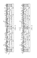
- FIG. 1 a shows semiconductor wafer 80 with a base substrate material 82 , such as silicon, germanium, aluminum phosphide, aluminum arsenide, gallium arsenide, gallium nitride, indium phosphide, silicon carbide, or other bulk semiconductor material for structural support.
- a plurality of semiconductor die 84 is formed on wafer 80 separated by a non-active, inter-die wafer area or saw street 86 .
- Saw street 86 provides cutting areas to singulate semiconductor wafer 80 into individual semiconductor die 84 .
- semiconductor wafer 80 has a width or diameter of 100-450 millimeters (mm) and thickness of 50-100 micrometers ( ⁇ m) or 15-250 ⁇ m.
- FIG. 1 b shows a cross-sectional view of a portion of semiconductor wafer 80 .
- Each semiconductor die 84 has a back or non-active surface 88 and an active surface or region 90 containing analog or digital circuits implemented as active devices, passive devices, conductive layers, and dielectric layers formed within the die and electrically interconnected according to the electrical design and function of the die.
- surface 88 may be a second active surface, opposite active surface 90 , containing analog or digital circuits implemented as active devices, passive devices, conductive layers, and dielectric layers formed within the die and electrically interconnected according to the electrical design and function of the die.
- the circuits may include one or more transistors, diodes, and other circuit elements formed within active surface or region 90 to implement analog circuits or digital circuits, such as DSP, microcontrollers, ASIC, standard logic, amplifiers, clock management, memory, interface circuits, and other signal processing circuit.
- Semiconductor die 84 may also contain integrated passive devices (IPDs), such as inductors, capacitors, and resistors, for RF signal processing.
- IPDs integrated passive devices
- An electrically conductive layer 92 is formed over active surface 90 using PVD, CVD, electrolytic plating, electroless plating process, evaporation, or other suitable metal deposition process.
- Conductive layer 92 includes one or more layers of aluminum (Al), copper (Cu), tin (Sn), nickel (Ni), gold (Au), silver (Ag), tungsten (W), titanium (Ti), titanium tungsten (TiW), or other suitable electrically conductive material.
- Conductive layer 92 operates as interconnect pads electrically connected to the circuits on active surface 90 .
- Semiconductor wafer 80 undergoes electrical testing and inspection as part of a quality control process.
- Manual visual inspection and automated optical systems are used to perform inspections on semiconductor wafer 80 .
- Software can be used in the automated optical analysis of semiconductor wafer 80 .
- Visual inspection methods may employ equipment such as a scanning electron microscope, high-intensity or ultra-violet light, metallurgical microscope, or optical microscope.
- Semiconductor wafer 80 is inspected for structural characteristics including warpage, thickness variation, surface particulates, irregularities, cracks, delamination, contamination, and discoloration.
- the active and passive components within semiconductor die 84 undergo testing at the wafer level for electrical performance and circuit function.
- Each semiconductor die 84 is tested for functionality and electrical parameters, as shown in FIG. 1 c , using a test probe head 94 including a plurality of probes or test leads 96 or other testing device.
- Semiconductor die 84 responds to the electrical stimuli, which is measured by computer test system 97 and compared to an expected response to test functionality of the semiconductor die.
- the electrical tests may include circuit functionality, lead integrity, resistivity, continuity, reliability, junction depth, ESD, RF performance, drive current, threshold current, leakage current, and operational parameters specific to the component type.
- the inspection and electrical testing of semiconductor wafer 80 enables semiconductor die 84 that pass to be designated as known good die for use in a semiconductor package.
- semiconductor wafer 80 is singulated through saw street 86 into individual semiconductor die 84 using saw blade or laser cutting tool 98 .
- semiconductor wafer 80 is singulated using plasma etching, which has advantages of removing base substrate material 82 to form precision surfaces, while retaining the structure and integrity of the base substrate material.
- semiconductor die 84 are memory circuits, image sensor processor (ISP), or other controller or signal processor.
- FIG. 2 a shows semiconductor wafer 100 with a base substrate material 102 , such as silicon, germanium, aluminum phosphide, aluminum arsenide, gallium arsenide, gallium nitride, indium phosphide, silicon carbide, or other bulk semiconductor material for structural support.
- a plurality of semiconductor die 104 is formed on wafer 100 separated by a non-active, inter-die wafer area or saw street 106 .
- Saw street 106 provides cutting areas to singulate semiconductor wafer 100 into individual semiconductor die 104 .
- semiconductor wafer 100 has a width or diameter of 100-450 mm and thickness of 100-250 ⁇ m.
- FIG. 2 b shows a cross-sectional view of a portion of semiconductor wafer 100 .
- Each semiconductor die 104 has a back or non-active surface 108 and an active surface or region 110 including an image sensor area 112 implemented as CCD and active pixel sensors in CMOS or NMOS technologies.
- Active surface or region 110 further contains analog or digital circuits implemented as active devices, passive devices, conductive layers, and dielectric layers formed within the die and electrically interconnected according to the electrical design and function of the die.
- An electrically conductive layer 114 is formed over active surface 110 using PVD, CVD, electrolytic plating, electroless plating process, evaporation, or other suitable metal deposition process.
- Conductive layer 114 includes one or more layers of Al, Cu, Sn, Ni, Au, Ag, W, Ti, TiW, or other suitable electrically conductive material.
- Conductive layer 114 operates as interconnect pads electrically connected to image sensor area 112 and the circuits on active surface 110 .
- Semiconductor wafer 100 undergoes electrical testing and inspection as part of a quality control process, similar to semiconductor wafer 80 .
- the inspection and electrical testing of semiconductor wafer 100 enables semiconductor die 104 that pass to be designated as known good die for use in a semiconductor package.
- FIGS. 3 a -3 j illustrate a process of forming a multi-die image sensor semiconductor package.
- a light transmissive wafer 130 is positioned over and aligned with semiconductor wafer 100 .
- light transmissive wafer 130 is made of glass or other optically transparent or translucent material.
- FIG. 3 b shows light transmissive wafer 130 disposed over semiconductor wafer 100 with adhesive material 132 , such as dry film or epoxy resin, while leaving space or gap 134 between semiconductor wafer 100 and light transmissive wafer 130 .
- Light transmissive wafer 130 passes light to image sensor area 112 .
- semiconductor wafer 100 is inverted and a portion of back surface 108 is removed by grinder 136 in a backgrinding operation.
- the backgrinding operation reduces a thickness of base substrate material 102 to surface 138 of the base substrate material.
- semiconductor wafer 100 has a post-grinding thickness of 50-100 ⁇ m.
- FIG. 3 d the individual semiconductor die 84 from FIGS. 1 a -1 d are positioned over semiconductor wafer 100 using a pick and place operation with surface 88 oriented toward back surface 108 .
- FIG. 3 e shows semiconductor die 84 bonded to surface 108 with die attach adhesive 140 , such as epoxy resin.
- an encapsulant or molding compound 144 is deposited over semiconductor wafer 100 and semiconductor die 84 as an insulating material using a compressive molding, transfer molding, liquid encapsulant molding, vacuum lamination, spin coating, or other suitable applicator.
- encapsulant 144 covers side surfaces of semiconductor die 84 .
- Encapsulant 144 can be polymer composite material, such as epoxy resin with filler, epoxy acrylate with filler, or polymer with proper filler.
- Encapsulant 144 is non-conductive and environmentally protects the semiconductor device from external elements and contaminants. Encapsulant 144 also protects semiconductor die 84 from degradation due to exposure to light.
- encapsulant 144 is removed by grinder 148 in a backgrinding operation.
- the backgrinding operation planarizes encapsulant 144 with semiconductor die 84 .
- a plurality of vias is formed through encapsulant 144 and semiconductor wafer 100 using mechanical drilling, laser drilling, or deep reactive ion etching (DRIE).
- the vias are filled with Al, Cu, Sn, Ni, Au, Ag, W, Ti, TiW, poly-silicon, or other suitable electrically conductive material using electrolytic plating, electroless plating process, or other suitable metal deposition process to form z-direction conductive through silicon vias (TSV) 150 embedded within encapsulant 144 and semiconductor wafer 100 outside image sensor area 112 .
- TSV 150 are electrically connected to image sensor area 112 and the conductive layers and circuits on active surface 110 of semiconductor die 104 .
- an insulating or passivation layer 154 is formed over encapsulant 144 and active surface 90 using PVD, CVD, printing, lamination, spin coating or spray coating.
- Insulating layer 154 contains one or more layers of silicon dioxide (SiO2), silicon nitride (Si3N4), silicon oxynitride (SiON), tantalum pentoxide (Ta2O5), aluminum oxide (Al2O3), solder resist, polyimide, benzocyclobutene (BCB), polybenzoxazoles (PBC)), polymer, or other material having similar insulating and structural properties.
- a portion of insulating layer 154 is removed by etching or laser direct ablation (LDA) to expose TSV 150 and conductive layer 92 on active surface 90 .
- LDA laser direct ablation
- An electrically conductive layer 156 is formed on insulating layer 154 using PVD, CVD, electrolytic plating, electroless plating process, evaporation, or other suitable metal deposition process.
- Conductive layer 156 includes one or more layers of Al, Cu, Sn, Ni, Au, Ag, Ti, TiW, or other suitable electrically conductive material.
- Conductive layer 156 operates as a first RDL for routing electrical signals from conductive layer 92 through TSV 150 to image sensor area 112 and the circuits on active surface 110 and active surface 90 , as well as external to the package.
- An insulating or passivation layer 158 is formed over insulating layer 154 and conductive layer 156 using PVD, CVD, printing, lamination, spin coating or spray coating.
- Insulating layer 158 contains one or more layers of SiO2, Si3N4, SiON, Ta2O5, Al2O3, solder resist, polyimide, BCB, PBO, polymer, or other material having similar insulating and structural properties.
- a portion of insulating layer 158 is removed by etching or LDA to expose conductive layer 156 .
- An electrically conductive layer 160 is formed on insulating layer 158 using PVD, CVD, electrolytic plating, electroless plating process, evaporation, or other suitable metal deposition process.
- Conductive layer 160 includes one or more layers of Al, Cu, Sn, Ni, Au, Ag, Ti, TiW, or other suitable electrically conductive material.
- Conductive layer 160 is electrically connected to conductive layer 156 and operates as a second RDL for routing electrical signals from conductive layer 92 through TSV 150 to image sensor area 112 and the circuits on active surface 110 and active surface 90 , as well as external to the package.
- An insulating or passivation layer 162 is formed over insulating layer 158 and conductive layer 160 using PVD, CVD, printing, lamination, spin coating or spray coating.
- Insulating layer 162 contains one or more layers of SiO2, Si3N4, SiON, Ta2O5, Al2O3, solder resist, polyimide, BCB, PBO, polymer, or other material having similar insulating and structural properties.
- a portion of insulating layer 162 is removed by etching or LDA to expose conductive layer 160 .
- Additional insulating layers such as 154 , 158 , and 162 , and conductive layers such as 156 and 160 , can be formed as multi-layered RDL build-up interconnect structure 168 .
- An electrically conductive bump material is deposited over conductive layer 160 using an evaporation, electrolytic plating, electroless plating, ball drop, or screen printing process.
- the bump material can be Al, Sn, Ni, Au, Ag, lead (Pb), bismuth (Bi), Cu, solder, and combinations thereof, with an optional flux solution.
- the bump material can be eutectic Sn/Pb, high-lead solder, or lead-free solder.
- the bump material is bonded to conductive layer 160 using a suitable attachment or bonding process.
- the bump material is reflowed by heating the material above its melting point to form balls or bumps 170 .
- bumps 170 are reflowed a second time to improve electrical contact to conductive layer 160 .
- bumps 170 are formed over an under bump metallization (UBM) layer.
- Bumps 170 can also be compression bonded or thermos-compression bonded to conductive layer 160 .
- Bumps 170 represent one type of interconnect structure that can be formed over conductive layer 160 .
- the interconnect structure can also use conductive pillar, stud bump, micro bump, bond wires, conductive paste, or other electrical interconnect.
- semiconductor wafer 100 is singulated through saw streets 106 with saw blade or laser cutting tool 174 or plasma etching process into individual semiconductor packages.
- FIGS. 4 a -4 b illustrate another embodiment for forming the build-up interconnect structure.
- an encapsulant 180 is formed over encapsulant 144 and active surface 90 , as shown in FIG. 4 a .
- a portion of encapsulant layer 180 is removed by etching or LDA to expose TSV 150 and conductive layer 92 on active surface 90 .
- An electrically conductive layer 186 is formed on encapsulant layer 180 using PVD, CVD, electrolytic plating, electroless plating process, evaporation, or other suitable metal deposition process.
- Conductive layer 186 includes one or more layers of Al, Cu, Sn, Ni, Au, Ag, Ti, TiW, or other suitable electrically conductive material.
- Conductive layer 186 operates as a first RDL for routing electrical signals from conductive layer 92 through TSV 150 to image sensor area 112 and the circuits on active surface 110 and active surface 90 , as well as external to the package.
- An encapsulant layer 188 is formed over encapsulant layer 180 and conductive layer 186 . A portion of encapsulant layer 188 is removed by etching or LDA to expose conductive layer 186 .
- An electrically conductive layer 190 is formed on encapsulant layer 188 using PVD, CVD, electrolytic plating, electroless plating process, evaporation, or other suitable metal deposition process. Conductive layer 190 includes one or more layers of Al, Cu, Sn, Ni, Au, Ag, Ti, TiW, or other suitable electrically conductive material.
- Conductive layer 190 is electrically connected to conductive layer 186 and operates as a second RDL for routing electrical signals from conductive layer 92 through TSV 150 to image sensor area 112 and the circuits on active surface 110 and active surface 90 , as well as external to the package.
- An encapsulant layer 192 is formed over encapsulant layer 188 and conductive layer 190 . A portion of encapsulant layer 192 is removed by etching or LDA to expose conductive layer 190 . Additional encapsulant layers such as 180 , 188 , and 192 , and conductive layers such as 186 and 190 , can be formed as multi-layered RDL build-up interconnect structure 194 .
- An electrically conductive bump material is deposited over conductive layer 190 using an evaporation, electrolytic plating, electroless plating, ball drop, or screen printing process.
- the bump material can be Al, Sn, Ni, Au, Ag, Pb, Bi, Cu, solder, and combinations thereof, with an optional flux solution.
- the bump material can be eutectic Sn/Pb, high-lead solder, or lead-free solder.
- the bump material is bonded to conductive layer 190 using a suitable attachment or bonding process.
- the bump material is reflowed by heating the material above its melting point to form balls or bumps 196 .
- bumps 196 are reflowed a second time to improve electrical contact to conductive layer 190 .
- bumps 196 are formed over a UBM layer.
- Bumps 196 can also be compression bonded or thermos-compression bonded to conductive layer 190 .
- Bumps 196 represent one type of interconnect structure that can be formed over conductive layer 190 .
- the interconnect structure can also use conductive pillar, stud bump, micro bump, bond wires, conductive paste, or other electrical interconnect.
- semiconductor wafer 100 is singulated through saw streets 106 with saw blade or laser cutting tool 198 or plasma etching process into individual semiconductor packages.
- FIG. 5 shows semiconductor package 200 post singulation.
- a portion of light transmissive wafer 130 is disposed over image sensor area 112 of semiconductor die 104 .
- TSV 150 electrically connect image sensor area 112 and the conductive layers and circuits on active surface 110 of semiconductor die 104 to build-up interconnect structure 168 or 194 as formed over encapsulant 144 and active surface 90 of semiconductor die 84 .
- the encapsulant in build-up interconnect structure 194 reduces stress for bumps 196 .
- Semiconductor package 200 integrates semiconductor die 84 and semiconductor die 104 to enhance the image performance within the multi-die image sensor package.
- the electrical routing path between semiconductor die 84 and semiconductor die 104 is reduced to improve signal propagation timing, reduce noise, and provide higher quality image sensing.
- FIGS. 6 a -6 b show electronic device 210 , such as a cellular phone with camera, which includes an image sensing device 212 implemented with semiconductor package 200 , as described in FIGS. 1-5 .
- FIG. 6 a represents the cellular phone with camera.
- FIG. 6 b is a functional block diagram of components within electronic device 210 .
- Electronic device 210 includes lens 214 for focusing an image on the pixel array within image sensing device 212 when a shutter release button 218 is touched or pressed.
- electronic device 210 includes central processing unit (CPU) 220 , such as a microprocessor, to control camera and image processing functions, input/output (I/O) device 222 , and memory 226 , which communicate with CPU 220 over bus 230 .
- CPU central processing unit
Landscapes
- Solid State Image Pick-Up Elements (AREA)
Abstract
Description
Claims (6)
Priority Applications (2)
| Application Number | Priority Date | Filing Date | Title |
|---|---|---|---|
| US15/407,224 US10103191B2 (en) | 2017-01-16 | 2017-01-16 | Semiconductor die and method of packaging multi-die with image sensor |
| CN201820032193.2U CN208256672U (en) | 2017-01-16 | 2018-01-09 | Image sensing semiconductor devices |
Applications Claiming Priority (1)
| Application Number | Priority Date | Filing Date | Title |
|---|---|---|---|
| US15/407,224 US10103191B2 (en) | 2017-01-16 | 2017-01-16 | Semiconductor die and method of packaging multi-die with image sensor |
Publications (2)
| Publication Number | Publication Date |
|---|---|
| US20180204866A1 US20180204866A1 (en) | 2018-07-19 |
| US10103191B2 true US10103191B2 (en) | 2018-10-16 |
Family
ID=62840875
Family Applications (1)
| Application Number | Title | Priority Date | Filing Date |
|---|---|---|---|
| US15/407,224 Active US10103191B2 (en) | 2017-01-16 | 2017-01-16 | Semiconductor die and method of packaging multi-die with image sensor |
Country Status (2)
| Country | Link |
|---|---|
| US (1) | US10103191B2 (en) |
| CN (1) | CN208256672U (en) |
Families Citing this family (8)
| Publication number | Priority date | Publication date | Assignee | Title |
|---|---|---|---|---|
| CN110291637B (en) * | 2017-02-22 | 2023-11-14 | 索尼半导体解决方案公司 | Imaging device, electronic device and method of manufacturing imaging device |
| US10522505B2 (en) * | 2017-04-06 | 2019-12-31 | Advanced Semiconductor Engineering, Inc. | Semiconductor device package and method for manufacturing the same |
| EP3442021A4 (en) * | 2017-06-07 | 2019-08-28 | Shenzhen Goodix Technology Co., Ltd. | CHIP ENCLOSURE STRUCTURE AND METHOD, AND TERMINAL DEVICE |
| US10930604B2 (en) | 2018-03-29 | 2021-02-23 | Semiconductor Components Industries, Llc | Ultra-thin multichip power devices |
| CN110473839B (en) * | 2018-05-11 | 2025-03-21 | 三星电子株式会社 | Semiconductor packaging system |
| US10707257B2 (en) * | 2018-08-14 | 2020-07-07 | Semiconductor Components Industries, Llc | Multi-chip packaging structure for an image sensor |
| US11088079B2 (en) | 2019-06-27 | 2021-08-10 | Taiwan Semiconductor Manufacturing Co., Ltd. | Package structure having line connected via portions |
| FR3099290B1 (en) * | 2019-07-26 | 2021-07-02 | Commissariat Energie Atomique | Method of collective curvature of a set of electronic chips |
Citations (13)
| Publication number | Priority date | Publication date | Assignee | Title |
|---|---|---|---|---|
| US20070054419A1 (en) | 2005-09-02 | 2007-03-08 | Kyung-Wook Paik | Wafer level chip size package for CMOS image sensor module and manufacturing method thereof |
| US20080191335A1 (en) * | 2007-02-08 | 2008-08-14 | Advanced Chip Engineering Technology Inc. | Cmos image sensor chip scale package with die receiving opening and method of the same |
| US20080217715A1 (en) | 2005-10-11 | 2008-09-11 | Park Tae-Seok | Wafer Level Package Using Silicon Via Contacts for Cmos Image Sensor and Method of Fabricating the Same |
| US20080308928A1 (en) * | 2007-06-13 | 2008-12-18 | Industrial Technology Research Institute | Image sensor module with a three-dimensional die-stacking structure |
| US20100032830A1 (en) * | 2008-08-06 | 2010-02-11 | Industrial Technology Research Institute | Three-dimensional conducting structure and method of fabricating the same |
| US20120313209A1 (en) * | 2011-06-09 | 2012-12-13 | Vage Oganesian | 3D Integrated Microelectronic Assembly With Stress Reducing Interconnects And Method Of Making Same |
| US20130221452A1 (en) * | 2011-09-15 | 2013-08-29 | Stats Chippac, Ltd. | Semiconductor Device and Method of Forming Semiconductor Die with Active Region Responsive to External Stimulus |
| US20150318323A1 (en) * | 2014-05-05 | 2015-11-05 | Semiconductor Components Industries, Llc | Image sensors with reduced stack height |
| US20160088243A1 (en) * | 2014-09-19 | 2016-03-24 | Kabushiki Kaisha Toshiba | Imaging element, imaging apparatus, and semiconductor apparatus |
| US20160172402A1 (en) * | 2014-12-11 | 2016-06-16 | Invensas Corporation | Image sensor device |
| US20170018590A1 (en) * | 2015-07-13 | 2017-01-19 | Xintec Inc. | Chip package and method for forming the same |
| US20170213864A1 (en) * | 2016-01-22 | 2017-07-27 | Omnivision Technologies, Inc. | Trenched-Bonding-Dam Device And Manufacturing Method For Same |
| US20170213920A1 (en) * | 2009-10-29 | 2017-07-27 | Sony Corporation | Semiconductor device, manufacturing method thereof, and electronic apparatus |
-
2017
- 2017-01-16 US US15/407,224 patent/US10103191B2/en active Active
-
2018
- 2018-01-09 CN CN201820032193.2U patent/CN208256672U/en active Active
Patent Citations (13)
| Publication number | Priority date | Publication date | Assignee | Title |
|---|---|---|---|---|
| US20070054419A1 (en) | 2005-09-02 | 2007-03-08 | Kyung-Wook Paik | Wafer level chip size package for CMOS image sensor module and manufacturing method thereof |
| US20080217715A1 (en) | 2005-10-11 | 2008-09-11 | Park Tae-Seok | Wafer Level Package Using Silicon Via Contacts for Cmos Image Sensor and Method of Fabricating the Same |
| US20080191335A1 (en) * | 2007-02-08 | 2008-08-14 | Advanced Chip Engineering Technology Inc. | Cmos image sensor chip scale package with die receiving opening and method of the same |
| US20080308928A1 (en) * | 2007-06-13 | 2008-12-18 | Industrial Technology Research Institute | Image sensor module with a three-dimensional die-stacking structure |
| US20100032830A1 (en) * | 2008-08-06 | 2010-02-11 | Industrial Technology Research Institute | Three-dimensional conducting structure and method of fabricating the same |
| US20170213920A1 (en) * | 2009-10-29 | 2017-07-27 | Sony Corporation | Semiconductor device, manufacturing method thereof, and electronic apparatus |
| US20120313209A1 (en) * | 2011-06-09 | 2012-12-13 | Vage Oganesian | 3D Integrated Microelectronic Assembly With Stress Reducing Interconnects And Method Of Making Same |
| US20130221452A1 (en) * | 2011-09-15 | 2013-08-29 | Stats Chippac, Ltd. | Semiconductor Device and Method of Forming Semiconductor Die with Active Region Responsive to External Stimulus |
| US20150318323A1 (en) * | 2014-05-05 | 2015-11-05 | Semiconductor Components Industries, Llc | Image sensors with reduced stack height |
| US20160088243A1 (en) * | 2014-09-19 | 2016-03-24 | Kabushiki Kaisha Toshiba | Imaging element, imaging apparatus, and semiconductor apparatus |
| US20160172402A1 (en) * | 2014-12-11 | 2016-06-16 | Invensas Corporation | Image sensor device |
| US20170018590A1 (en) * | 2015-07-13 | 2017-01-19 | Xintec Inc. | Chip package and method for forming the same |
| US20170213864A1 (en) * | 2016-01-22 | 2017-07-27 | Omnivision Technologies, Inc. | Trenched-Bonding-Dam Device And Manufacturing Method For Same |
Also Published As
| Publication number | Publication date |
|---|---|
| CN208256672U (en) | 2018-12-18 |
| US20180204866A1 (en) | 2018-07-19 |
Similar Documents
| Publication | Publication Date | Title |
|---|---|---|
| US10103191B2 (en) | Semiconductor die and method of packaging multi-die with image sensor | |
| US12230559B2 (en) | Semiconductor device and method of forming micro interconnect structures | |
| US11257729B2 (en) | Semiconductor device and method of forming encapsulated wafer level chip scale package (eWLCSP) | |
| JP6102941B2 (en) | Optical device and manufacturing method thereof | |
| KR101466450B1 (en) | Methods and apparatus for sensor module | |
| US9379072B2 (en) | Chip package and method for forming the same | |
| US12154877B2 (en) | Semiconductor wafer and method of ball drop on thin wafer with edge support ring | |
| TW201838131A (en) | Semiconductor device and method of depositing an encapsulant along the sides and surface edges of a semiconductor die in a buried wafer level wafer size package | |
| US20230036239A1 (en) | Semiconductor Device and Method of Making an Optical Semiconductor Package | |
| US12302657B2 (en) | Semiconductor device and method of forming an optical semiconductor package with a shield structure | |
| US20240339484A1 (en) | Semiconductor Device and Method of Making an Optical Semiconductor Package | |
| US20230343668A1 (en) | Semiconductor Packages and Methods of Forming RDL and Side and Back Protection for Semiconductor Device | |
| US20230192478A1 (en) | Semiconductor Device and Method of Making a MEMS Semiconductor Package | |
| US20210167112A1 (en) | Fanout wafer level package for optical devices and related methods |
Legal Events
| Date | Code | Title | Description |
|---|---|---|---|
| AS | Assignment |
Owner name: SEMICONDUCTOR COMPONENTS INDUSTRIES, LLC, ARIZONA Free format text: ASSIGNMENT OF ASSIGNORS INTEREST;ASSIGNOR:HSIEH, YU-TE;REEL/FRAME:040978/0620 Effective date: 20170113 |
|
| AS | Assignment |
Owner name: DEUTSCHE BANK AG NEW YORK BRANCH, AS COLLATERAL AGENT, NEW YORK Free format text: PATENT SECURITY AGREEMENT;ASSIGNORS:SEMICONDUCTOR COMPONENTS INDUSTRIES, LLC;FAIRCHILD SEMICONDUCTOR CORPORATION;REEL/FRAME:044481/0541 Effective date: 20170504 Owner name: DEUTSCHE BANK AG NEW YORK BRANCH, AS COLLATERAL AG Free format text: PATENT SECURITY AGREEMENT;ASSIGNORS:SEMICONDUCTOR COMPONENTS INDUSTRIES, LLC;FAIRCHILD SEMICONDUCTOR CORPORATION;REEL/FRAME:044481/0541 Effective date: 20170504 |
|
| STCF | Information on status: patent grant |
Free format text: PATENTED CASE |
|
| MAFP | Maintenance fee payment |
Free format text: PAYMENT OF MAINTENANCE FEE, 4TH YEAR, LARGE ENTITY (ORIGINAL EVENT CODE: M1551); ENTITY STATUS OF PATENT OWNER: LARGE ENTITY Year of fee payment: 4 |
|
| AS | Assignment |
Owner name: FAIRCHILD SEMICONDUCTOR CORPORATION, ARIZONA Free format text: RELEASE OF SECURITY INTEREST IN PATENTS RECORDED AT REEL 04481, FRAME 0541;ASSIGNOR:DEUTSCHE BANK AG NEW YORK BRANCH, AS COLLATERAL AGENT;REEL/FRAME:064072/0459 Effective date: 20230622 Owner name: SEMICONDUCTOR COMPONENTS INDUSTRIES, LLC, ARIZONA Free format text: RELEASE OF SECURITY INTEREST IN PATENTS RECORDED AT REEL 04481, FRAME 0541;ASSIGNOR:DEUTSCHE BANK AG NEW YORK BRANCH, AS COLLATERAL AGENT;REEL/FRAME:064072/0459 Effective date: 20230622 |