US10087371B2 - Liquid crystal composition and liquid crystal display including the same - Google Patents
Liquid crystal composition and liquid crystal display including the same Download PDFInfo
- Publication number
- US10087371B2 US10087371B2 US15/407,699 US201715407699A US10087371B2 US 10087371 B2 US10087371 B2 US 10087371B2 US 201715407699 A US201715407699 A US 201715407699A US 10087371 B2 US10087371 B2 US 10087371B2
- Authority
- US
- United States
- Prior art keywords
- liquid crystal
- chemical formula
- compound represented
- crystal compound
- fluorine
- Prior art date
- Legal status (The legal status is an assumption and is not a legal conclusion. Google has not performed a legal analysis and makes no representation as to the accuracy of the status listed.)
- Active
Links
- 0 *.B.C.CCC1CC2=C(C3=C(C=C2)CC(CC)C3(C)C)C(C)C1C.[1*]C.[2*]C.[2HH] Chemical compound *.B.C.CCC1CC2=C(C3=C(C=C2)CC(CC)C3(C)C)C(C)C1C.[1*]C.[2*]C.[2HH] 0.000 description 8
- YZHCMVNBJOVVOZ-UHFFFAOYSA-N CC.CC.CC.CC.CC.CC.CC.CC.CC.CC.CC1=CCC(C)CC1.CC1C=CC(C)CC1.CC1CCC(C)CC1.CC1CCC(C)OC1.CC1OC(C)C(C)C(C)O1.Cc1ccc(C)cc1 Chemical compound CC.CC.CC.CC.CC.CC.CC.CC.CC.CC.CC1=CCC(C)CC1.CC1C=CC(C)CC1.CC1CCC(C)CC1.CC1CCC(C)OC1.CC1OC(C)C(C)C(C)O1.Cc1ccc(C)cc1 YZHCMVNBJOVVOZ-UHFFFAOYSA-N 0.000 description 8
- MEGZRSXZVVNFEL-ULWDQGEZSA-J C/C=C/C1CCC(C2CCC(C)CC2)CC1.C=CC1CCC(C2CCC(C)CC2)CC1.C=CC1CCC(C2CCC(C3=CC=C([Y])C=C3)CC2)CC1.CC1=CC=C(C2=CC=C(O[Y])C(F)=C2F)C=C1.CC1CCC(C2=CC=C(O[Y])C(F)=C2F)CC1.CC1CCC(C2=CC=C(O[Y])C=C2)CC1.CC1CCC(C2=CC=C([Y])C=C2)CC1.CC1CCC(C2CCC(C3=CC=C(O[Y])C(F)=C3F)CC2)CC1.CC1CCC(C2CCC(C3=CC=C([Y])C(F)=C3F)CC2)CC1.CC1CCC(C2CCC(O[Y])CC2)CC1.CC1CCC(C2CCC([Y])CC2)CC1 Chemical compound C/C=C/C1CCC(C2CCC(C)CC2)CC1.C=CC1CCC(C2CCC(C)CC2)CC1.C=CC1CCC(C2CCC(C3=CC=C([Y])C=C3)CC2)CC1.CC1=CC=C(C2=CC=C(O[Y])C(F)=C2F)C=C1.CC1CCC(C2=CC=C(O[Y])C(F)=C2F)CC1.CC1CCC(C2=CC=C(O[Y])C=C2)CC1.CC1CCC(C2=CC=C([Y])C=C2)CC1.CC1CCC(C2CCC(C3=CC=C(O[Y])C(F)=C3F)CC2)CC1.CC1CCC(C2CCC(C3=CC=C([Y])C(F)=C3F)CC2)CC1.CC1CCC(C2CCC(O[Y])CC2)CC1.CC1CCC(C2CCC([Y])CC2)CC1 MEGZRSXZVVNFEL-ULWDQGEZSA-J 0.000 description 5
- OFKQUQYBNNLMIK-UHFFFAOYSA-K CC1=CC(F)=C(C2=CC=C(C3=CC=C([Y])C=C3)C=C2)C=C1.CC1=CC=C(C2=CC=C(C3=CC(F)=C(C4=CC(F)=C([Y])C(F)=C4)C=C3)C=C2)C=C1.CC1=CC=C(C2=CC=C(O[Y])C=C2)C=C1.CC1=CC=C(C2=CC=C([Y])C=C2)C=C1.CC1CCC(C2=CC=C(C3=CC=C([Y])C(F)=C3F)C=C2)CC1.CC1CCC(C2CCC(COC3=CC=C(O[Y])C(F)=C3F)CC2)CC1.CC1CCC(COC2=CC=C(O[Y])C(F)=C2F)CC1 Chemical compound CC1=CC(F)=C(C2=CC=C(C3=CC=C([Y])C=C3)C=C2)C=C1.CC1=CC=C(C2=CC=C(C3=CC(F)=C(C4=CC(F)=C([Y])C(F)=C4)C=C3)C=C2)C=C1.CC1=CC=C(C2=CC=C(O[Y])C=C2)C=C1.CC1=CC=C(C2=CC=C([Y])C=C2)C=C1.CC1CCC(C2=CC=C(C3=CC=C([Y])C(F)=C3F)C=C2)CC1.CC1CCC(C2CCC(COC3=CC=C(O[Y])C(F)=C3F)CC2)CC1.CC1CCC(COC2=CC=C(O[Y])C(F)=C2F)CC1 OFKQUQYBNNLMIK-UHFFFAOYSA-K 0.000 description 5
- VRZYMJFEYRIQDB-UHFFFAOYSA-N CCCC1=CC=C(C2=CC3=C(C(F)=C2F)C2=C(C=C3)C=C(CC)C2(F)F)C=C1.CCCC1=CC=C(C2=CC3=C(C(F)=C2F)C2=C(C=C3)C=C(CC)C2F)C=C1.CCCC1=CC=C(C2=CC3=C(C(F)=C2F)C2=C(C=C3)CC(OCC)C2(F)F)C=C1.CCCC1=CC=C(C2=CC3=C(C(F)=C2F)C2=C(C=C3)CC(OCC)C2F)C=C1 Chemical compound CCCC1=CC=C(C2=CC3=C(C(F)=C2F)C2=C(C=C3)C=C(CC)C2(F)F)C=C1.CCCC1=CC=C(C2=CC3=C(C(F)=C2F)C2=C(C=C3)C=C(CC)C2F)C=C1.CCCC1=CC=C(C2=CC3=C(C(F)=C2F)C2=C(C=C3)CC(OCC)C2(F)F)C=C1.CCCC1=CC=C(C2=CC3=C(C(F)=C2F)C2=C(C=C3)CC(OCC)C2F)C=C1 VRZYMJFEYRIQDB-UHFFFAOYSA-N 0.000 description 5
- CFJCNWQXOICKIF-UHFFFAOYSA-N CCCC1CCC(C2CCC(C3=CC=C(OCC)C(F)=C3F)CC2)CC1 Chemical compound CCCC1CCC(C2CCC(C3=CC=C(OCC)C(F)=C3F)CC2)CC1 CFJCNWQXOICKIF-UHFFFAOYSA-N 0.000 description 3
- QYGWJCMCLQAINT-UHFFFAOYSA-N CCCCC1CCC(C2CCC(CCC)CC2)CC1 Chemical compound CCCCC1CCC(C2CCC(CCC)CC2)CC1 QYGWJCMCLQAINT-UHFFFAOYSA-N 0.000 description 3
- IASLDLGGHXYCEO-HWKANZROSA-N C/C=C/C1CCC(C2CCC(CCC)CC2)CC1 Chemical compound C/C=C/C1CCC(C2CCC(CCC)CC2)CC1 IASLDLGGHXYCEO-HWKANZROSA-N 0.000 description 2
- KHDBEDDPFRHGCN-UHFFFAOYSA-N C=CC1CCC(C2CCC(CCC)CC2)CC1 Chemical compound C=CC1CCC(C2CCC(CCC)CC2)CC1 KHDBEDDPFRHGCN-UHFFFAOYSA-N 0.000 description 2
- PJMJYILDKOHNBZ-UHFFFAOYSA-N CC.CC.CC.CC.CC.CC.CC.CC.CC.CC.CC1=CCC(C)CC1.CC1C=CC(C)CC1.CC1CCC(C)CC1.CC1CCC(C)OC1.CC1OC(C)C(C)C(C)O1.c1ccccc1 Chemical compound CC.CC.CC.CC.CC.CC.CC.CC.CC.CC.CC1=CCC(C)CC1.CC1C=CC(C)CC1.CC1CCC(C)CC1.CC1CCC(C)OC1.CC1OC(C)C(C)C(C)O1.c1ccccc1 PJMJYILDKOHNBZ-UHFFFAOYSA-N 0.000 description 2
- RYPOSVPGRBGCKW-UHFFFAOYSA-N CCCC1=CC=C(C2=CC=C(OCC)C(F)=C2F)C=C1 Chemical compound CCCC1=CC=C(C2=CC=C(OCC)C(F)=C2F)C=C1 RYPOSVPGRBGCKW-UHFFFAOYSA-N 0.000 description 2
- IBFAIOMGVHPWRQ-UHFFFAOYSA-N CCCC1CCC(C2=CC=C(C3=CC=C(OCC)C(F)=C3F)C=C2)CC1 Chemical compound CCCC1CCC(C2=CC=C(C3=CC=C(OCC)C(F)=C3F)C=C2)CC1 IBFAIOMGVHPWRQ-UHFFFAOYSA-N 0.000 description 2
- KORMYSCDCHFFMN-UHFFFAOYSA-N CCCC1CCC(C2CCC(CC)CC2)CC1 Chemical compound CCCC1CCC(C2CCC(CC)CC2)CC1 KORMYSCDCHFFMN-UHFFFAOYSA-N 0.000 description 2
- GLZNOTOAQDMKMM-UHFFFAOYSA-N CCCCCC1CCC(C2CCC(C3=CC=C(OCC)C(F)=C3F)CC2)CC1 Chemical compound CCCCCC1CCC(C2CCC(C3=CC=C(OCC)C(F)=C3F)CC2)CC1 GLZNOTOAQDMKMM-UHFFFAOYSA-N 0.000 description 2
- KYNDSYARZOJNCG-UHFFFAOYSA-N CCCCOC1=CC=C(C2CCC(CCC)CC2)C(F)=C1F Chemical compound CCCCOC1=CC=C(C2CCC(CCC)CC2)C(F)=C1F KYNDSYARZOJNCG-UHFFFAOYSA-N 0.000 description 2
- DEFRYXBKOCRIJE-UHFFFAOYSA-N CCOC1=CC=C(C2=CC=C(C3CCC(CC)CC3)C=C2)C(F)=C1F Chemical compound CCOC1=CC=C(C2=CC=C(C3CCC(CC)CC3)C=C2)C(F)=C1F DEFRYXBKOCRIJE-UHFFFAOYSA-N 0.000 description 2
- ADPYSZNUBWNLDH-UHFFFAOYSA-N CC1C=CC(C)CC1 Chemical compound CC1C=CC(C)CC1 ADPYSZNUBWNLDH-UHFFFAOYSA-N 0.000 description 1
- KMGDYKOGDOVDCW-UHFFFAOYSA-N CC1CC=C(C)CC1 Chemical compound CC1CC=C(C)CC1 KMGDYKOGDOVDCW-UHFFFAOYSA-N 0.000 description 1
- QRMPKOFEUHIBNM-UHFFFAOYSA-N CC1CCC(C)CC1 Chemical compound CC1CCC(C)CC1 QRMPKOFEUHIBNM-UHFFFAOYSA-N 0.000 description 1
- YEJCHVFCLNKZPU-UHFFFAOYSA-N CC1COC(C)CC1 Chemical compound CC1COC(C)CC1 YEJCHVFCLNKZPU-UHFFFAOYSA-N 0.000 description 1
- GRHYNNJHMNXNFP-UHFFFAOYSA-N CCCC1=CC=C(C2=CC3=C(C(F)=C2F)C2=C(C=C3)CC(OCC)C2(F)F)C=C1 Chemical compound CCCC1=CC=C(C2=CC3=C(C(F)=C2F)C2=C(C=C3)CC(OCC)C2(F)F)C=C1 GRHYNNJHMNXNFP-UHFFFAOYSA-N 0.000 description 1
- ALSCPZRLSDLPES-UHFFFAOYSA-N CCCC1=CC=C(C2=CC=C(C3=CC=C(CC)C=C3)C(F)=C2F)C=C1 Chemical compound CCCC1=CC=C(C2=CC=C(C3=CC=C(CC)C=C3)C(F)=C2F)C=C1 ALSCPZRLSDLPES-UHFFFAOYSA-N 0.000 description 1
- UCJYOYBGPOTCBB-UHFFFAOYSA-N CCCC1=CC=C(C2=CC=C3C4=C(C(F)=C(F)C3=C2F)C(F)C(OCC)C4)C=C1 Chemical compound CCCC1=CC=C(C2=CC=C3C4=C(C(F)=C(F)C3=C2F)C(F)C(OCC)C4)C=C1 UCJYOYBGPOTCBB-UHFFFAOYSA-N 0.000 description 1
Images


Classifications
-
- C—CHEMISTRY; METALLURGY
- C09—DYES; PAINTS; POLISHES; NATURAL RESINS; ADHESIVES; COMPOSITIONS NOT OTHERWISE PROVIDED FOR; APPLICATIONS OF MATERIALS NOT OTHERWISE PROVIDED FOR
- C09K—MATERIALS FOR MISCELLANEOUS APPLICATIONS, NOT PROVIDED FOR ELSEWHERE
- C09K19/00—Liquid crystal materials
- C09K19/04—Liquid crystal materials characterised by the chemical structure of the liquid crystal components, e.g. by a specific unit
- C09K19/06—Non-steroidal liquid crystal compounds
- C09K19/32—Non-steroidal liquid crystal compounds containing condensed ring systems, i.e. fused, bridged or spiro ring systems
- C09K19/322—Compounds containing a naphthalene ring or a completely or partially hydrogenated naphthalene ring
-
- C—CHEMISTRY; METALLURGY
- C07—ORGANIC CHEMISTRY
- C07C—ACYCLIC OR CARBOCYCLIC COMPOUNDS
- C07C25/00—Compounds containing at least one halogen atom bound to a six-membered aromatic ring
- C07C25/18—Polycyclic aromatic halogenated hydrocarbons
- C07C25/22—Polycyclic aromatic halogenated hydrocarbons with condensed rings
-
- C—CHEMISTRY; METALLURGY
- C07—ORGANIC CHEMISTRY
- C07C—ACYCLIC OR CARBOCYCLIC COMPOUNDS
- C07C43/00—Ethers; Compounds having groups, groups or groups
- C07C43/02—Ethers
- C07C43/18—Ethers having an ether-oxygen atom bound to a carbon atom of a ring other than a six-membered aromatic ring
- C07C43/192—Ethers having an ether-oxygen atom bound to a carbon atom of a ring other than a six-membered aromatic ring containing halogen
-
- G—PHYSICS
- G02—OPTICS
- G02F—OPTICAL DEVICES OR ARRANGEMENTS FOR THE CONTROL OF LIGHT BY MODIFICATION OF THE OPTICAL PROPERTIES OF THE MEDIA OF THE ELEMENTS INVOLVED THEREIN; NON-LINEAR OPTICS; FREQUENCY-CHANGING OF LIGHT; OPTICAL LOGIC ELEMENTS; OPTICAL ANALOGUE/DIGITAL CONVERTERS
- G02F1/00—Devices or arrangements for the control of the intensity, colour, phase, polarisation or direction of light arriving from an independent light source, e.g. switching, gating or modulating; Non-linear optics
- G02F1/01—Devices or arrangements for the control of the intensity, colour, phase, polarisation or direction of light arriving from an independent light source, e.g. switching, gating or modulating; Non-linear optics for the control of the intensity, phase, polarisation or colour
- G02F1/13—Devices or arrangements for the control of the intensity, colour, phase, polarisation or direction of light arriving from an independent light source, e.g. switching, gating or modulating; Non-linear optics for the control of the intensity, phase, polarisation or colour based on liquid crystals, e.g. single liquid crystal display cells
- G02F1/133—Constructional arrangements; Operation of liquid crystal cells; Circuit arrangements
- G02F1/1333—Constructional arrangements; Manufacturing methods
- G02F1/1343—Electrodes
- G02F1/134309—Electrodes characterised by their geometrical arrangement
-
- G—PHYSICS
- G02—OPTICS
- G02F—OPTICAL DEVICES OR ARRANGEMENTS FOR THE CONTROL OF LIGHT BY MODIFICATION OF THE OPTICAL PROPERTIES OF THE MEDIA OF THE ELEMENTS INVOLVED THEREIN; NON-LINEAR OPTICS; FREQUENCY-CHANGING OF LIGHT; OPTICAL LOGIC ELEMENTS; OPTICAL ANALOGUE/DIGITAL CONVERTERS
- G02F1/00—Devices or arrangements for the control of the intensity, colour, phase, polarisation or direction of light arriving from an independent light source, e.g. switching, gating or modulating; Non-linear optics
- G02F1/01—Devices or arrangements for the control of the intensity, colour, phase, polarisation or direction of light arriving from an independent light source, e.g. switching, gating or modulating; Non-linear optics for the control of the intensity, phase, polarisation or colour
- G02F1/13—Devices or arrangements for the control of the intensity, colour, phase, polarisation or direction of light arriving from an independent light source, e.g. switching, gating or modulating; Non-linear optics for the control of the intensity, phase, polarisation or colour based on liquid crystals, e.g. single liquid crystal display cells
- G02F1/133—Constructional arrangements; Operation of liquid crystal cells; Circuit arrangements
- G02F1/1333—Constructional arrangements; Manufacturing methods
- G02F1/1343—Electrodes
- G02F1/13439—Electrodes characterised by their electrical, optical, physical properties; materials therefor; method of making
-
- G—PHYSICS
- G02—OPTICS
- G02F—OPTICAL DEVICES OR ARRANGEMENTS FOR THE CONTROL OF LIGHT BY MODIFICATION OF THE OPTICAL PROPERTIES OF THE MEDIA OF THE ELEMENTS INVOLVED THEREIN; NON-LINEAR OPTICS; FREQUENCY-CHANGING OF LIGHT; OPTICAL LOGIC ELEMENTS; OPTICAL ANALOGUE/DIGITAL CONVERTERS
- G02F1/00—Devices or arrangements for the control of the intensity, colour, phase, polarisation or direction of light arriving from an independent light source, e.g. switching, gating or modulating; Non-linear optics
- G02F1/01—Devices or arrangements for the control of the intensity, colour, phase, polarisation or direction of light arriving from an independent light source, e.g. switching, gating or modulating; Non-linear optics for the control of the intensity, phase, polarisation or colour
- G02F1/13—Devices or arrangements for the control of the intensity, colour, phase, polarisation or direction of light arriving from an independent light source, e.g. switching, gating or modulating; Non-linear optics for the control of the intensity, phase, polarisation or colour based on liquid crystals, e.g. single liquid crystal display cells
- G02F1/133—Constructional arrangements; Operation of liquid crystal cells; Circuit arrangements
- G02F1/136—Liquid crystal cells structurally associated with a semi-conducting layer or substrate, e.g. cells forming part of an integrated circuit
- G02F1/1362—Active matrix addressed cells
- G02F1/1368—Active matrix addressed cells in which the switching element is a three-electrode device
-
- G—PHYSICS
- G02—OPTICS
- G02F—OPTICAL DEVICES OR ARRANGEMENTS FOR THE CONTROL OF LIGHT BY MODIFICATION OF THE OPTICAL PROPERTIES OF THE MEDIA OF THE ELEMENTS INVOLVED THEREIN; NON-LINEAR OPTICS; FREQUENCY-CHANGING OF LIGHT; OPTICAL LOGIC ELEMENTS; OPTICAL ANALOGUE/DIGITAL CONVERTERS
- G02F1/00—Devices or arrangements for the control of the intensity, colour, phase, polarisation or direction of light arriving from an independent light source, e.g. switching, gating or modulating; Non-linear optics
- G02F1/01—Devices or arrangements for the control of the intensity, colour, phase, polarisation or direction of light arriving from an independent light source, e.g. switching, gating or modulating; Non-linear optics for the control of the intensity, phase, polarisation or colour
- G02F1/13—Devices or arrangements for the control of the intensity, colour, phase, polarisation or direction of light arriving from an independent light source, e.g. switching, gating or modulating; Non-linear optics for the control of the intensity, phase, polarisation or colour based on liquid crystals, e.g. single liquid crystal display cells
- G02F1/137—Devices or arrangements for the control of the intensity, colour, phase, polarisation or direction of light arriving from an independent light source, e.g. switching, gating or modulating; Non-linear optics for the control of the intensity, phase, polarisation or colour based on liquid crystals, e.g. single liquid crystal display cells characterised by the electro-optical or magneto-optical effect, e.g. field-induced phase transition, orientation effect, guest-host interaction or dynamic scattering
-
- C07C2103/16—
-
- C—CHEMISTRY; METALLURGY
- C07—ORGANIC CHEMISTRY
- C07C—ACYCLIC OR CARBOCYCLIC COMPOUNDS
- C07C2603/00—Systems containing at least three condensed rings
- C07C2603/02—Ortho- or ortho- and peri-condensed systems
- C07C2603/04—Ortho- or ortho- and peri-condensed systems containing three rings
- C07C2603/06—Ortho- or ortho- and peri-condensed systems containing three rings containing at least one ring with less than six ring members
- C07C2603/10—Ortho- or ortho- and peri-condensed systems containing three rings containing at least one ring with less than six ring members containing five-membered rings
- C07C2603/12—Ortho- or ortho- and peri-condensed systems containing three rings containing at least one ring with less than six ring members containing five-membered rings only one five-membered ring
- C07C2603/16—Benz[e]indenes; Hydrogenated benz[e]indenes
-
- G—PHYSICS
- G02—OPTICS
- G02F—OPTICAL DEVICES OR ARRANGEMENTS FOR THE CONTROL OF LIGHT BY MODIFICATION OF THE OPTICAL PROPERTIES OF THE MEDIA OF THE ELEMENTS INVOLVED THEREIN; NON-LINEAR OPTICS; FREQUENCY-CHANGING OF LIGHT; OPTICAL LOGIC ELEMENTS; OPTICAL ANALOGUE/DIGITAL CONVERTERS
- G02F1/00—Devices or arrangements for the control of the intensity, colour, phase, polarisation or direction of light arriving from an independent light source, e.g. switching, gating or modulating; Non-linear optics
- G02F1/01—Devices or arrangements for the control of the intensity, colour, phase, polarisation or direction of light arriving from an independent light source, e.g. switching, gating or modulating; Non-linear optics for the control of the intensity, phase, polarisation or colour
- G02F1/13—Devices or arrangements for the control of the intensity, colour, phase, polarisation or direction of light arriving from an independent light source, e.g. switching, gating or modulating; Non-linear optics for the control of the intensity, phase, polarisation or colour based on liquid crystals, e.g. single liquid crystal display cells
- G02F1/133—Constructional arrangements; Operation of liquid crystal cells; Circuit arrangements
- G02F1/1333—Constructional arrangements; Manufacturing methods
- G02F1/1343—Electrodes
- G02F1/134309—Electrodes characterised by their geometrical arrangement
- G02F1/134345—Subdivided pixels, e.g. for grey scale or redundancy
-
- G—PHYSICS
- G02—OPTICS
- G02F—OPTICAL DEVICES OR ARRANGEMENTS FOR THE CONTROL OF LIGHT BY MODIFICATION OF THE OPTICAL PROPERTIES OF THE MEDIA OF THE ELEMENTS INVOLVED THEREIN; NON-LINEAR OPTICS; FREQUENCY-CHANGING OF LIGHT; OPTICAL LOGIC ELEMENTS; OPTICAL ANALOGUE/DIGITAL CONVERTERS
- G02F1/00—Devices or arrangements for the control of the intensity, colour, phase, polarisation or direction of light arriving from an independent light source, e.g. switching, gating or modulating; Non-linear optics
- G02F1/01—Devices or arrangements for the control of the intensity, colour, phase, polarisation or direction of light arriving from an independent light source, e.g. switching, gating or modulating; Non-linear optics for the control of the intensity, phase, polarisation or colour
- G02F1/13—Devices or arrangements for the control of the intensity, colour, phase, polarisation or direction of light arriving from an independent light source, e.g. switching, gating or modulating; Non-linear optics for the control of the intensity, phase, polarisation or colour based on liquid crystals, e.g. single liquid crystal display cells
- G02F1/137—Devices or arrangements for the control of the intensity, colour, phase, polarisation or direction of light arriving from an independent light source, e.g. switching, gating or modulating; Non-linear optics for the control of the intensity, phase, polarisation or colour based on liquid crystals, e.g. single liquid crystal display cells characterised by the electro-optical or magneto-optical effect, e.g. field-induced phase transition, orientation effect, guest-host interaction or dynamic scattering
- G02F1/13712—Devices or arrangements for the control of the intensity, colour, phase, polarisation or direction of light arriving from an independent light source, e.g. switching, gating or modulating; Non-linear optics for the control of the intensity, phase, polarisation or colour based on liquid crystals, e.g. single liquid crystal display cells characterised by the electro-optical or magneto-optical effect, e.g. field-induced phase transition, orientation effect, guest-host interaction or dynamic scattering the liquid crystal having negative dielectric anisotropy
-
- G02F2001/134345—
-
- G02F2001/13712—
-
- G—PHYSICS
- G02—OPTICS
- G02F—OPTICAL DEVICES OR ARRANGEMENTS FOR THE CONTROL OF LIGHT BY MODIFICATION OF THE OPTICAL PROPERTIES OF THE MEDIA OF THE ELEMENTS INVOLVED THEREIN; NON-LINEAR OPTICS; FREQUENCY-CHANGING OF LIGHT; OPTICAL LOGIC ELEMENTS; OPTICAL ANALOGUE/DIGITAL CONVERTERS
- G02F2201/00—Constructional arrangements not provided for in groups G02F1/00 - G02F7/00
- G02F2201/12—Constructional arrangements not provided for in groups G02F1/00 - G02F7/00 electrode
- G02F2201/121—Constructional arrangements not provided for in groups G02F1/00 - G02F7/00 electrode common or background
-
- G—PHYSICS
- G02—OPTICS
- G02F—OPTICAL DEVICES OR ARRANGEMENTS FOR THE CONTROL OF LIGHT BY MODIFICATION OF THE OPTICAL PROPERTIES OF THE MEDIA OF THE ELEMENTS INVOLVED THEREIN; NON-LINEAR OPTICS; FREQUENCY-CHANGING OF LIGHT; OPTICAL LOGIC ELEMENTS; OPTICAL ANALOGUE/DIGITAL CONVERTERS
- G02F2201/00—Constructional arrangements not provided for in groups G02F1/00 - G02F7/00
- G02F2201/12—Constructional arrangements not provided for in groups G02F1/00 - G02F7/00 electrode
- G02F2201/123—Constructional arrangements not provided for in groups G02F1/00 - G02F7/00 electrode pixel
-
- G—PHYSICS
- G02—OPTICS
- G02F—OPTICAL DEVICES OR ARRANGEMENTS FOR THE CONTROL OF LIGHT BY MODIFICATION OF THE OPTICAL PROPERTIES OF THE MEDIA OF THE ELEMENTS INVOLVED THEREIN; NON-LINEAR OPTICS; FREQUENCY-CHANGING OF LIGHT; OPTICAL LOGIC ELEMENTS; OPTICAL ANALOGUE/DIGITAL CONVERTERS
- G02F2202/00—Materials and properties
- G02F2202/42—Materials having a particular dielectric constant
Definitions
- Embodiments relate to a liquid crystal composition and a liquid crystal display including the same.
- a liquid crystal display is one among widely-used display devices.
- the liquid crystal display may have two display panels on which field generating electrodes, such as pixel electrodes and a common electrode, are formed, and a liquid crystal layer that is interposed between the display panels.
- field generating electrodes such as pixel electrodes and a common electrode
- a voltage may be applied to the field generating electrodes so as to form an electric field in the liquid crystal layer
- the alignment of liquid crystal molecules of the liquid crystal layer may be determined by the electric field
- the polarization of incident light may be controlled.
- Embodiments are directed to a liquid crystal composition and a liquid crystal display including the same.
- the embodiments may be realized by providing a liquid crystal composition comprising a liquid crystal compound represented by Chemical Formula 1 below:
- X 1 to X 4 are each independently hydrogen, fluorine, or an alkyl group
- Z 1 and Z 2 are each independently a single bond, a double bond, CF 2 CF 2 , or OCF 2
- R 1 is hydrogen, fluorine, or an alkyl group
- R 2 is hydrogen, fluorine, an alkyl group, or an alkoxy group
- A is
- B is cyclohexane, cyclohexene, or benzene
- C is cyclopentane or cyclopentene
- X 5 , X 6 , X 7 , and X 8 in A and D are each independently hydrogen, fluorine, or an alkyl group
- p is an integer of 1 to 4
- q is an integer of 0 to 3
- n is an integer of 1 to 4.
- the liquid crystal compound represented by Chemical Formula 1 may include a liquid crystal compound represented by one of Chemical Formula 1-1 to 1-4:
- a dielectric anisotropy ( ⁇ ) of the liquid crystal compound represented by Chemical Formula 1 may be ⁇ 4 to ⁇ 5, and a rotation viscosity ( ⁇ 1) of the liquid crystal compound represented by Chemical Formula 1 may be about 150 or less.
- a phase transition temperature (Tni) of the liquid crystal compound represented by Chemical Formula 1 may be 95° C. to 105° C., and a refractive anisotropy ( ⁇ n) of the liquid crystal compound represented by Chemical Formula 1 may be 0.2 to 0.3.
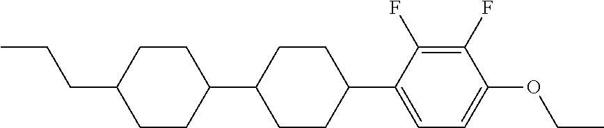
- the liquid crystal composition may further include a liquid crystal compound represented by one of Chemical Formula 2 to Chemical Formula 19:
- X and Y are each independently a C1 to C4 alkyl group.
- a dielectric anisotropy ( ⁇ ) of the liquid crystal composition may be ⁇ 3 to ⁇ 4.
- a rotation viscosity ( ⁇ 1) of the liquid crystal composition may be about 120 or less.
- the embodiments may be realized by providing a liquid crystal display including a first substrate; a second substrate separated from and overlapping the first substrate; and a liquid crystal layer positioned between the first substrate and the second substrate, wherein the liquid crystal layer includes a liquid crystal compound represented by Chemical Formula 1:
- X 1 to X 4 are each independently hydrogen, fluorine, or an alkyl group
- Z 1 and Z 2 are each independently a single bond, a double bond, CF 2 CF 2 , or OCF 2
- R 1 is hydrogen, fluorine, or an alkyl group
- R 2 is hydrogen, fluorine, an alkyl group, or an alkoxy group
- A is
- B is cyclohexane, cyclohexene, or benzene
- C is cyclopentane or cyclopentene
- X 5 , X 6 , X 7 , and X 8 in A and D are each independently hydrogen, fluorine, or an alkyl group
- p is an integer of 1 to 4
- q is an integer of 0 to 3
- n is an integer of 1 to 4.
- the liquid crystal compound represented by Chemical Formula 1 may include a liquid crystal compound represented by one of Chemical Formula 1-1 to 1-4:
- a dielectric anisotropy ( ⁇ ) of the liquid crystal compound represented by Chemical Formula 1 may be ⁇ 4 to ⁇ 5, and a rotation viscosity ( ⁇ 1) of the liquid crystal compound represented by Chemical Formula 1 may be about 150 or less.
- a phase transition temperature (Tni) of the liquid crystal compound represented by Chemical Formula 1 may be 95° C. to 105° C., and a refractive anisotropy ( ⁇ n) of the liquid crystal compound represented by Chemical Formula 1 may be 0.2 to 0.3.
- the liquid crystal layer may further include a liquid crystal compound represented by one of Chemical Formula 2 to Chemical Formula 19:
- X and Y are each independently a C1 to C4 alkyl group.
- a dielectric anisotropy ( ⁇ ) of the liquid crystal composition may be ⁇ 3 to ⁇ 4.
- a rotation viscosity ( ⁇ 1) of the liquid crystal composition may be about 120 or less.
- the liquid crystal display may further include a thin film transistor on the first substrate; a pixel electrode connected to the thin film transistor; and a common electrode forming an electric field with the pixel electrode.
- the pixel electrode may include a cross-shaped stem and a minute branch extending from the cross-shaped stem.
- FIG. 1 illustrates a plan layout view of a pixel of a liquid crystal display according to an exemplary embodiment.
- FIG. 2 illustrates a cross-sectional view taken along a line II-II of FIG. 1 .
- FIG. 1 illustrates a plan layout view of a pixel of a liquid crystal display according to an exemplary embodiment
- FIG. 2 illustrates a cross-sectional view taken along a line II-II of FIG. 1 .
- the liquid crystal display may include a lower panel 100 , an upper panel 200 facing and separated from the lower panel 100 , and a liquid crystal layer 3 positioned between the lower panel 100 and the upper panel 200 .
- the liquid crystal composition according to an exemplary embodiment may include, e.g., a liquid crystal compound represented by Chemical Formula 1 below.
- X 1 to X 4 may each independently be or include, e.g., hydrogen (H), fluorine (F), or an alkyl group (e.g., C n H 2n+1 ).
- suitable substituents may be included on any of the described groups.
- X 1 to X 4 may each independently be or include, e.g., a methyl group (CH 3 ) or a trifluoromethyl group (CF 3 ).
- Z 1 and Z 2 may each independently be or include, e.g., a single bond, a double bond, CF 2 CF 2 , or OCF 2 .
- R 1 may be or may include, e.g., hydrogen (H), fluorine (F), or an alkyl group (e.g., C n H 2n+1 ).
- R 2 may be or may include, e.g., hydrogen (H), fluorine (F), an alkyl group (e.g., C n H 2n+1 ), or an alkoxy group (e.g., OC n H 2n+1 ).
- A may be or may include, e.g.,
- D may be or may include, e.g.,
- B may be or may include, e.g., a cyclohexane, a cyclohexene, or a benzene.
- C may be or may include, e.g., a cyclopentane or a cyclopentene.
- B may be or may include, e.g., a cyclohexene, or a benzene and/or C may be or may include, e.g., a cyclopentene.
- B and C may each share a bond with the core benzene moiety shown in Chemical Formula 1 and form a fused ring structure therewith.
- X 5 , X 6 , X 7 , and X 8 in A and D may each independently be or include, e.g., hydrogen (H), fluorine (F), or an alkyl group (e.g., C n H 2n+1 ).
- p may be, e.g., an integer of 1 to 4
- q may be, e.g., an integer of 0 to 3
- n may be, e.g., an integer of 1 to 4.
- a dielectric anisotropy ( ⁇ ) of the liquid crystal compound represented by Chemical Formula 1 may be, e.g., ⁇ 4 to ⁇ 5.
- a rotation viscosity ( ⁇ 1) of the liquid crystal compound represented by Chemical Formula 1 may be, e.g., about 50 to about 150. Maintaining the rotation viscosity ( ⁇ 1) of the liquid crystal compound at about 50 or greater may help ensure that a physical property required by the liquid crystal layer is satisfied.
- a phase transition temperature (Tni) of the liquid crystal compound represented by Chemical Formula 1 may be 95° C. to 105° C.
- a refractive anisotropy ( ⁇ n) of the liquid crystal compound represented by Chemical Formula 1 may be 0.2 to 0.3.
- the liquid crystal compound represented by Chemical Formula 1 may be included in the liquid crystal composition in an amount of, e.g., about 1 to 20 wt %, based on a total weight of the liquid crystal composition.
- the liquid crystal compound represented by Chemical Formula 1 may include, e.g., a liquid crystal compound represented by one of the following Chemical Formulae 1-1 to 1-4.
- the liquid crystal compound represented by Chemical Formula 1-1 to Chemical Formula 1-4 may satisfy the physical properties of the liquid crystal compound represented by Chemical Formula 1.
- the refractive anisotropy ( ⁇ n) may be 0.258
- the dielectric anisotropy ( ⁇ ) may be ⁇ 4.25
- the rotation viscosity ( ⁇ 1) may be about 149.6
- the phase transition temperature (Tni) may be 98.4° C.
- the refractive anisotropy ( ⁇ n) may be 0.249, the dielectric anisotropy ( ⁇ ) may be ⁇ 4.83, the rotation viscosity ( ⁇ 1) may be about 123.3, and the phase transition temperature (Tni) may be 102.9° C.
- the refractive anisotropy ( ⁇ n) may be 0.267, the dielectric anisotropy ( ⁇ ) may be ⁇ 4.22, the rotation viscosity ( ⁇ 1) may be about 120.5, and the phase transition temperature (Tni) may be 95.2° C.
- the refractive anisotropy ( ⁇ n) may be 0.258
- the dielectric anisotropy ( ⁇ ) may be ⁇ 4.83
- the rotation viscosity ( ⁇ 1) may be about 93.3
- the phase transition temperature (Tni) may be 99.7° C.
- the liquid crystal compound represented by Chemical Formula 1 may include three rings, e.g., fused rings, positioned at a center of a molecular structure.
- at least one hydrogen (H) connected to the cyclopentane ring or the cyclopentene ring may be substituted with fluorine (F), e.g., one or both of X 3 or X 4 may be or may include F.
- hydrogen connected to the phenyl ring may not be substituted with fluorine (F), etc. If a hydrogen on the phenyl ring were to be substituted or replaced with fluorine, the center of the molecular structure could be formed to be bulky such that the rotation viscosity could increase, and the response speed may be disadvantageous.
- the phenyl ring structure positioned at the center of the molecular structure may not include fluorine, etc., and the structure of the C ring (e.g., cyclopentane ring or the cyclopentene ring) connected to the phenyl ring may include a fluorine or fluorine-containing substituent.
- the low rotation viscosity may be obtained while obtaining the dielectric anisotropy of the same level.
- the refractive anisotropy ( ⁇ n) may be 0.249
- the dielectric anisotropy ( ⁇ ) may be ⁇ 4.83
- the rotation viscosity ( ⁇ 1) may be about 123.3
- the phase transition temperature (Tni) may be 102.9° C.
- the refractive anisotropy ( ⁇ n) may be 0.251
- the dielectric anisotropy ( ⁇ ) may be ⁇ 4.97
- the rotation viscosity ( ⁇ 1) may be about 224.3
- the phase transition temperature (Tni) may be 91.7° C.
- the rotation viscosity ( ⁇ 1) of the liquid crystal compound represented by Chemical Formula 1-2 may be about 50% lower relative to the liquid crystal compound of Chemical Formula (1-2a).
- the liquid crystal compound according to an exemplary embodiment may have the improved rotation viscosity and improved response speed depending on an application of a voltage.
- Equation 1 is an equation related to the rotation viscosity ( ⁇ 1), the rotation viscosity ( ⁇ 1) being proportional to a square of an order parameter (S), and the order parameter (S) decreases as a dipole moment increases. For example, as the dipole moment increases, the order parameter (S) may be decreased, and accordingly, the rotation viscosity ( ⁇ 1) may also be decreased.
- liquid crystal compound represented by Chemical Formula 1-2 may have a dipole moment of about 0.136, and the liquid crystal compound represented by Chemical Formula (1-2a) may have a dipole moment of about 0.118.
- the liquid crystal composition according to an exemplary embodiment may have a high dipole moment compared with another liquid crystal composition, and accordingly the liquid crystal composition may have a low order parameter (S), thereby having a low rotation viscosity ( ⁇ 1).
- the liquid crystal composition according to an exemplary embodiment may further include a liquid crystal compound represented by one of the following Chemical Formula 2 to Chemical Formula 19.
- X and Y may each independently be or include, e.g., an alkyl group (e.g., C n′ H 2n′+1 , in which n′ in X and Y is independently a natural number of 1 to 4).
- an alkyl group e.g., C n′ H 2n′+1 , in which n′ in X and Y is independently a natural number of 1 to 4).
- the liquid crystal compound represented by Chemical Formula 2 may be included in the composition in an amount of about 10 to 30 wt % for the entire content of the liquid crystal composition (e.g., based on a total weight of the composition).
- the liquid crystal compound represented by Chemical Formula 3 may be included in the composition in an amount of about 5 to 15 wt % for the entire content of the liquid crystal composition.
- the liquid crystal compound represented by Chemical Formula 4 may be included in the composition in an amount of about 3 to 10 wt % for the entire content of the liquid crystal composition.
- the liquid crystal compound represented by Chemical Formula 5 may be included in the composition in an amount of about 10 to 35 wt % for the entire content of the liquid crystal composition.
- the liquid crystal compound represented by Chemical Formula 6 may be included in the composition in an amount of about 5 to 15 wt % for the entire content of the liquid crystal composition.
- the liquid crystal compound represented by Chemical Formula 7 may be included in the composition in an amount of about 5 to 15 wt % for the entire content of the liquid crystal composition.
- the liquid crystal compound represented by Chemical Formula 8 may be included in the composition in an amount of about 3 to 25 wt % for the entire content of the liquid crystal composition.
- the liquid crystal compound represented by Chemical Formula 9 may be included in the composition in an amount of about 5 to 25 wt % for the entire content of the liquid crystal composition.
- the liquid crystal compound represented by Chemical Formula 10 may be included in the composition in an amount of about 5 to 20 wt % for the entire content of the liquid crystal composition.
- the liquid crystal compound represented by Chemical Formula 11 may be included in the composition in an amount of about 5 to 20 wt % for the entire content of the liquid crystal composition.
- the liquid crystal compound represented by Chemical Formula 12 may be included in the composition in an amount of about 5 to 25 wt % for the entire content of the liquid crystal composition.
- the liquid crystal compound represented by Chemical Formula 13 may be included in the composition in an amount of about 5 to 25 wt % for the entire content of the liquid crystal composition.
- the liquid crystal compound represented by Chemical Formula 14 may be included in the composition in an amount of about 0.03 to 5 wt % for the entire content of the liquid crystal composition.
- the liquid crystal compounds represented by Chemical Formula 15 to Chemical Formula 19 may be included in an amount suitable to satisfy the physical properties required by the liquid crystal composition.
- the liquid crystal compound represented by Chemical Formula 1 may be included in an amount of, e.g., about 1 to 20 wt %, based on the total weight of the liquid crystal composition.
- at least one among the compounds represented by Chemical Formula 2 to 19 may be included in the liquid crystal composition to satisfy the above-described content, thereby providing the liquid crystal composition for the liquid crystal display having a predetermined physical property.
- the dielectric anisotropy ( ⁇ ) of the liquid crystal composition may be, e.g., ⁇ 3 to ⁇ 4, and the rotation viscosity ( ⁇ 1) of the liquid crystal composition may be, e.g., about 50 to about 120.
- the refractive anisotropy ( ⁇ n) of the liquid crystal composition may be, e.g., 0.08 to 0.15, and the phase transition temperature (Tni) may be, e.g., about 55 to 130° C.
- the above-described liquid crystal composition may have negative dielectric anisotropy, and may include the liquid crystal compounds representing the low rotation viscosity such that improved response speed may be provided.
- a gate conductor including a gate line 121 and a voltage dividing reference voltage line 131 may be formed on an insulating substrate 110 formed of transparent glass, plastics, or the like.
- the gate line 121 may include a first gate electrode 124 a , a second gate electrode 124 b , and a third gate electrode 124 c.
- the voltage dividing reference voltage line 131 may include first storage electrodes 135 and 136 , and a reference electrode 137 . Second storage electrodes 138 and 139 that are not connected to the voltage dividing reference voltage line 131 may be positioned to overlap a second subpixel electrode 191 b.
- a gate insulating layer 140 may be positioned on the gate line 121 and the voltage dividing reference voltage line 131 .
- a first semiconductor layer 154 a , a second semiconductor layer 154 b , and a third semiconductor layer 154 c may be positioned on the gate insulating layer 140 .
- a plurality of ohmic contacts 163 a . 165 a , 163 b , 165 b , 163 c , and 165 c may be formed on the semiconductors 154 a , 154 b , and 154 c.
- a data conductor including a data line 171 connected to a first source electrode 173 a and a second source electrode 173 b , a first drain electrode 175 a , a second drain electrode 175 b , a third source electrode 173 c , and a third drain electrode 175 c may be positioned on the ohmic contacts 163 a , 165 a , 163 b , 165 b , 163 c , and 165 c and the gate insulating layer 140 .
- the data conductor and the underlying semiconductor layers 154 a , 154 b , and 154 c and ohmic contacts 163 a , 165 a , 163 b , 165 b , 163 c , and 165 c may be simultaneously formed by using one mask.
- the first gate electrode 124 a , the first source electrode 173 a , and the first drain electrode 175 a may form a first thin film transistor along with the first semiconductor layer 154 a
- the second gate electrode 124 b , the second source electrode 173 b , and the second drain electrode 175 b form a second thin film transistor along with the second semiconductor layer 154 b
- the third gate electrode 124 c , the third source electrode 173 c , and the third drain electrode 175 c form a third thin film transistor along with the third semiconductor layer 154 c.
- the second drain electrode 175 b may be connected with the third source electrode 173 c , and includes an extended portion 177 that is widely extended.
- a first passivation layer 180 p may be formed on the data conductors 171 , 173 c , 175 a , 175 b , and 175 c and exposed portions of the semiconductors 154 a , 154 b , and 154 c .
- the first passivation layer 180 p may include an inorganic insulating layer, such as a silicon nitride or a silicon oxide.
- a color filter 230 may be positioned on the first passivation layer 180 p .
- the color filter 230 may be extended in a vertical direction along two adjacent data lines.
- the color filter 230 may be positioned in the lower panel 100 or the color filter 230 may be positioned in the upper panel 200 .
- a second passivation layer 180 q may be positioned on the color filter 230 .
- the second passivation layer 180 q may include the inorganic insulating layer such as a silicon nitride or a silicon oxide.
- the second passivation layer 180 q may help prevent the color filter 230 from being peeled, and may help suppress contamination of the liquid crystal layer 3 by an organic material such as a solvent flowing in from the color filter 230 , thereby preventing defects such as an afterimage that may occur when a screen is driven.
- the first passivation layer 180 p and the second passivation layer 180 q may have a first contact hole 185 a and a second contact hole 185 b respectively exposing the first drain electrode 175 a and the second drain electrode 175 b.
- the first passivation layer 180 p , the second passivation layer 180 q , and the gate insulating layer 140 may have a third contact hole 185 c exposing a part of the reference electrode 137 and a part of the third drain electrode 175 c , and the third contact hole 185 c may be covered by a connecting member 195 .
- the connecting member 195 may electrically connect the reference electrode 137 and the third drain electrode 175 c that are exposed through the third contact hole 185 c.
- a plurality of pixel electrodes 191 may be positioned on the second passivation layer 180 q .
- the pixel electrode 191 may be one field generating electrode, and each pixel electrode 191 may include a first subpixel electrode 191 a and the second subpixel electrode 191 b that may be separated from each other with the gate line 121 interposed therebetween, and may be adjacent in a column direction based on the gate line 121 .
- the pixel electrode 191 may be made of a transparent material such as ITO or IZO.
- the overall shape of the first subpixel electrode 191 a and the second subpixel electrode 191 b may be a quadrangle, and they respectively may include a cross-shaped stem having a transverse stem 193 and a longitudinal stem 192 that are crossed.
- the first subpixel electrode 191 a and the second subpixel electrode 191 b may be respectively divided into a first sub-region Da, a second sub-region Db, a third sub-region Dc, and a fourth sub-region Dd by the transverse stem 193 and the longitudinal stem 192 , and each of the sub-regions Da-Dd include a plurality of minute branches.
- the first subpixel electrode 191 a and the second subpixel electrode 191 b may be respectively connected to the first drain electrode 175 a and the second drain electrode 175 b through the first contact hole 185 a and the second contact hole 185 b , respectively, and may receive the data voltage from the first drain electrode 175 a and the second drain electrode 175 b , respectively.
- a part of the data voltage applied to the second drain electrode 175 b may be divided through the third source electrode 173 c , so that a magnitude of the voltage applied to the first subpixel electrode 191 a may be larger than that of the voltage applied to the second subpixel electrode 192 b.
- sides of the minute branches 194 may distort an electric field and form a horizontal component that determines an inclination direction of the liquid crystal molecules 31 .
- the horizontal component of the electric field may be almost horizontal to the sides of the first to fourth minute branches 194 .
- the liquid crystal molecules 31 may be inclined in a direction parallel to the longitudinal direction of the minute branches 194 .
- One pixel electrode 191 may include four subregions Da to Dd in which longitudinal directions of the minute branches 194 are different from each other, and the directions in which the liquid crystal molecules 31 are inclined are about four directions, and four domains, in which the alignment directions of the liquid crystal molecules 31 are different from each other, may be formed in the liquid crystal layer 3 .
- a reference viewing angle of the liquid crystal display may be increased.
- the first subpixel electrode 191 a and the second subpixel electrode 191 b may generate an electric field together with a common electrode 270 of the upper panel 200 , thereby determining orientation of the liquid crystal molecules 31 of the liquid crystal layer 3 between the two electrodes 191 and 270 .
- Luminance of light passing through the liquid crystal layer 3 may vary depending on the determined orientation of the liquid crystal molecules 31 .
- the aforementioned description of the thin film transistor and the pixel electrode 191 is just an example, and a structure of the thin film transistor and a design of the pixel electrode can be modified to improve side visibility.
- a first alignment layer 11 may be positioned on the pixel electrode 191 , and the first alignment layer 11 may be a vertical alignment layer.
- the first alignment layer 11 may be formed to include at least one among general materials used as a liquid crystal alignment layer such as a polyamic acid or a polyimide.
- a second substrate 210 may be positioned to be separated from the first substrate 110 .
- a light blocking member 220 may be positioned between the second substrate 210 and the liquid crystal layer 3 .
- the light blocking member 220 may be positioned in the upper panel 200 to overlap a region where the data line 171 of the lower panel 100 is positioned and a region where the thin film transistor is positioned.
- the light blocking member 220 may be positioned in the upper panel 200 or may be positioned in the lower panel 100 .
- an overcoat 250 may be positioned between the light blocking member 220 and the liquid crystal layer 3 .
- the overcoat 250 may be omitted.
- the common electrode 270 that is one of the field generating electrodes may be positioned between the overcoat 250 and the liquid crystal layer 3 .
- the common electrode 270 generates the electric field along with the pixel electrode 191 of the lower panel 100 , the direction of the liquid crystal molecules 31 of the liquid crystal layer 3 may be determined.
- a second alignment layer 21 may be positioned between the common electrode 270 and the liquid crystal layer 3 , and the second alignment layer 21 may be a vertical alignment layer.
- the second alignment layer 21 may be formed of the same material as the first alignment layer 11 .
- the liquid crystal layer 3 may be positioned between the first alignment layer 11 and the second alignment layer 21 .
- the liquid crystal layer 3 may include the liquid crystal composition according to an exemplary embodiment having the negative dielectric anisotropy.
- the liquid crystal molecules 31 of the liquid crystal layer 3 may be aligned to be perpendicular to the surfaces of the two display panels 100 and 200 with respect to their long axes when no electric field is applied.
- the liquid crystal layer 3 of the display according an exemplary embodiment may include a compound such as monomer or the like which is cured by polymerization due to light such as ultraviolet rays, or the like.
- the compound may be the reactive mesogen polymerized by light such as ultraviolet rays, or the like.
- the above-mentioned reactive mesogen may be polymerized depending on a manufacturing process to thereby form a polymer, and the liquid crystal molecules 31 are aligned so as to have a pre-tile by the polymer.
- Example liquid crystal composition including the liquid crystal compound represented by Chemical Formula 1 and a Comparative Example liquid crystal composition without it are compared with each other.
- Example and Comparative Example are provided in order to highlight characteristics of one or more embodiments, but it will be understood that the Example and Comparative Example are not to be construed as limiting the scope of the embodiments, nor is the Comparative Example to be construed as being outside the scope of the embodiments. Further, it will be understood that the embodiments are not limited to the particular details described in the Example and Comparative Example.
- the Example liquid crystal composition according to Table 1 includes the liquid crystal compound represented by Chemical Formula 1
- the Comparative Example liquid crystal composition according to Table 2 is the liquid crystal composition in which the liquid crystal compound represented by Chemical Formula 1 is not included.
- the refractive anisotropy ( ⁇ n) was about 0.105
- the dielectric anisotropy ( ⁇ ) was about ⁇ 3.22
- the rotation viscosity ( ⁇ 1) was about 119
- the phase transition temperature (Tni) was about 74° C.
- the refractive anisotropy ( ⁇ n) was about 0.106
- the dielectric anisotropy ( ⁇ ) was about ⁇ 3.13
- the rotation viscosity ( ⁇ 1) was about 124
- the phase transition temperature (Tni) was about 74° C.
- Example liquid crystal composition including the compound represented by Chemical Formula 1 may provide the low rotation viscosity while maintaining almost the same level as the Comparative Example liquid crystal composition for other physical properties. Accordingly, the response speed of the liquid crystal display including the Example liquid crystal composition may be improved.
- the liquid crystal display may include a liquid crystal material that is suitable to control the transmittance of light and obtain desired images.
- various characteristics such as low voltage driving, a high voltage holding ratio (VHR), a wide viewing angle characteristic, a wide range of operation temperature, and high speed response may be desirable.
- the embodiments may provide a liquid crystal composition having a low rotation viscosity. Also, a response speed that is improved through the liquid crystal display including the same may be provided.
- the liquid crystal composition having the low rotation viscosity may be provided, and the response speed of the liquid crystal display including the same may be improved.
Landscapes
- Chemical & Material Sciences (AREA)
- Physics & Mathematics (AREA)
- Organic Chemistry (AREA)
- Nonlinear Science (AREA)
- Crystallography & Structural Chemistry (AREA)
- General Physics & Mathematics (AREA)
- Optics & Photonics (AREA)
- Engineering & Computer Science (AREA)
- Mathematical Physics (AREA)
- Materials Engineering (AREA)
- Geometry (AREA)
- Microelectronics & Electronic Packaging (AREA)
- Liquid Crystal Substances (AREA)
Abstract

Description


D is

B is cyclohexane, cyclohexene, or benzene, C is cyclopentane or cyclopentene, X5, X6, X7, and X8 in A and D are each independently hydrogen, fluorine, or an alkyl group, p is an integer of 1 to 4, q is an integer of 0 to 3, and n is an integer of 1 to 4.


D is

B is cyclohexane, cyclohexene, or benzene, C is cyclopentane or cyclopentene, X5, X6, X7, and X8 in A and D are each independently hydrogen, fluorine, or an alkyl group, p is an integer of 1 to 4, q is an integer of 0 to 3, and n is an integer of 1 to 4.


D may be or may include, e.g.,

B may be or may include, e.g., a cyclohexane, a cyclohexene, or a benzene. C may be or may include, e.g., a cyclopentane or a cyclopentene. In an implementation, B may be or may include, e.g., a cyclohexene, or a benzene and/or C may be or may include, e.g., a cyclopentene. For example, B and C may each share a bond with the core benzene moiety shown in Chemical Formula 1 and form a fused ring structure therewith. X5, X6, X7, and X8 in A and D may each independently be or include, e.g., hydrogen (H), fluorine (F), or an alkyl group (e.g., CnH2n+1). p may be, e.g., an integer of 1 to 4, q may be, e.g., an integer of 0 to 3, and n may be, e.g., an integer of 1 to 4.


| TABLE 1 | |
| Chemical Formula | Content (wt %) |
 |
3-25 |
 |
3-25 |
 |
5-20 |
 |
5-25 |
 |
3-25 |
|
|
5-30 |
 |
5-25 |
|
|
10-30 |
|
|
5-15 |
|
|
5-30 |
 |
5-25 |
| TABLE 2 | |
| Chemical Formula | Content (wt %) |
 |
3-25 |
 |
3-25 |
 |
5-20 |
 |
5-25 |
 |
3-25 |
|
|
5-30 |
 |
5-25 |
|
|
10-30 |
|
|
5-15 |
|
|
5-30 |
 |
5-25 |
Claims (16)


Applications Claiming Priority (2)
| Application Number | Priority Date | Filing Date | Title |
|---|---|---|---|
| KR1020160007007A KR102511837B1 (en) | 2016-01-20 | 2016-01-20 | Liquid crystal composition and liquid crystal display comprising the same |
| KR10-2016-0007007 | 2016-01-20 |
Publications (2)
| Publication Number | Publication Date |
|---|---|
| US20170204331A1 US20170204331A1 (en) | 2017-07-20 |
| US10087371B2 true US10087371B2 (en) | 2018-10-02 |
Family
ID=59313360
Family Applications (1)
| Application Number | Title | Priority Date | Filing Date |
|---|---|---|---|
| US15/407,699 Active US10087371B2 (en) | 2016-01-20 | 2017-01-17 | Liquid crystal composition and liquid crystal display including the same |
Country Status (2)
| Country | Link |
|---|---|
| US (1) | US10087371B2 (en) |
| KR (1) | KR102511837B1 (en) |
Citations (7)
| Publication number | Priority date | Publication date | Assignee | Title |
|---|---|---|---|---|
| US20030108684A1 (en) * | 2001-09-17 | 2003-06-12 | Clariant International Ltd. | Fluorinated cyclopenta[a]naphthalenes and their use in liquid-crystal mixtures |
| US20060165915A1 (en) | 2002-08-26 | 2006-07-27 | Lars Lietzau | Cyclopenta[b]naphthalene derivatives |
| US20060202163A1 (en) | 2003-08-22 | 2006-09-14 | Lars Lietzau | Cyclopenta[a]naphthaline derivatives |
| US20080071097A1 (en) | 2004-07-29 | 2008-03-20 | Andreas Taugerbeck | Difluorosubstituted Heterocyclic Compounds and the Use Thereof in the Form of Components in Liquid Crystalline Media |
| KR20090040902A (en) | 2006-07-26 | 2009-04-27 | 메르크 파텐트 게엠베하 | Fused Naphthalene Compound |
| US20130310558A1 (en) | 2012-05-16 | 2013-11-21 | Brummond Key M | Synthesis, structure and use of functionalized naphthalenes |
| US8801966B2 (en) | 2008-02-08 | 2014-08-12 | Vvi Bright China Ltd. | Liquid crystals comprising cyclopentane groups |
Family Cites Families (1)
| Publication number | Priority date | Publication date | Assignee | Title |
|---|---|---|---|---|
| KR20140014990A (en) * | 2012-07-27 | 2014-02-06 | 삼성디스플레이 주식회사 | Liquid crystal composition and liquid crystal display |
-
2016
- 2016-01-20 KR KR1020160007007A patent/KR102511837B1/en active Active
-
2017
- 2017-01-17 US US15/407,699 patent/US10087371B2/en active Active
Patent Citations (9)
| Publication number | Priority date | Publication date | Assignee | Title |
|---|---|---|---|---|
| US20030108684A1 (en) * | 2001-09-17 | 2003-06-12 | Clariant International Ltd. | Fluorinated cyclopenta[a]naphthalenes and their use in liquid-crystal mixtures |
| US20060165915A1 (en) | 2002-08-26 | 2006-07-27 | Lars Lietzau | Cyclopenta[b]naphthalene derivatives |
| US20060202163A1 (en) | 2003-08-22 | 2006-09-14 | Lars Lietzau | Cyclopenta[a]naphthaline derivatives |
| US7575785B2 (en) * | 2003-08-22 | 2009-08-18 | Merck Patent Gmbh | Cyclopenta[a]naphthaline derivatives |
| US20080071097A1 (en) | 2004-07-29 | 2008-03-20 | Andreas Taugerbeck | Difluorosubstituted Heterocyclic Compounds and the Use Thereof in the Form of Components in Liquid Crystalline Media |
| KR20090040902A (en) | 2006-07-26 | 2009-04-27 | 메르크 파텐트 게엠베하 | Fused Naphthalene Compound |
| US20100059711A1 (en) | 2006-07-26 | 2010-03-11 | Merck Patent Gesellschaft Mit Beschrankter Haftung | Fused naphthalenes |
| US8801966B2 (en) | 2008-02-08 | 2014-08-12 | Vvi Bright China Ltd. | Liquid crystals comprising cyclopentane groups |
| US20130310558A1 (en) | 2012-05-16 | 2013-11-21 | Brummond Key M | Synthesis, structure and use of functionalized naphthalenes |
Non-Patent Citations (1)
| Title |
|---|
| Gwozdz, et al. "Influence of Dipole-Dipole Interactions on Structural Properties of Gay-Berne Particles", Acta Physica Polonica A No. 5 vol. 95 (2000) pp. 645-649. |
Also Published As
| Publication number | Publication date |
|---|---|
| KR102511837B1 (en) | 2023-03-20 |
| KR20170087565A (en) | 2017-07-31 |
| US20170204331A1 (en) | 2017-07-20 |
Similar Documents
| Publication | Publication Date | Title |
|---|---|---|
| KR102069822B1 (en) | Liquid crystal display and manufacturing method thereof | |
| US9261733B2 (en) | Liquid crystal display device and method for producing the same | |
| US8153208B2 (en) | Liquid crystal display, a method for manufacturing a liquid crystal display and a liquid crystal composition | |
| US20110051065A1 (en) | Liquid crystal device and manufacturing method of the same | |
| US10558087B2 (en) | Liquid crystal display and manufacturing method thereof | |
| US10527890B2 (en) | Liquid crystal display and manufacturing method thereof | |
| US9507209B2 (en) | Liquid crystal display device and method for manufacturing the same | |
| US20160209707A1 (en) | Liquid crystal display and manufacturing method of making the liquid crystal display | |
| US9567527B2 (en) | Alignment layer and liquid crystal display including the same | |
| US9977288B2 (en) | Liquid crystal display | |
| US20170031213A1 (en) | Liquid crystal display | |
| US9454040B2 (en) | Liquid crystal display | |
| US20160326434A1 (en) | Liquid crystal composition and liquid crystal display including the same | |
| US10100250B2 (en) | Liquid crystal display | |
| US10087371B2 (en) | Liquid crystal composition and liquid crystal display including the same | |
| US9890249B2 (en) | Photoalignment agent and liquid crystal display device including the same | |
| US20170015904A1 (en) | Liquid crystal composition and liquid crystal display including the same | |
| US20160209708A1 (en) | Liquid crystal display and method of manufacturing the same | |
| US10620480B2 (en) | Liquid crystal display | |
| US9605205B2 (en) | Liquid crystal composition and liquid crystal display including the same | |
| US10647918B2 (en) | Liquid crystal composition and display device including the same | |
| US10723949B2 (en) | Liquid crystal composition and display device including the same | |
| US20170081587A1 (en) | Liquid crystal composition and liquid crystal display device including the same | |
| US10106739B2 (en) | Liquid crystal composition and liquid crystal display device comprising the same | |
| US9902905B2 (en) | Liquid crystal composition and liquid crystal display including the same |
Legal Events
| Date | Code | Title | Description |
|---|---|---|---|
| AS | Assignment |
Owner name: SAMSUNG DISPLAY CO., LTD., KOREA, REPUBLIC OF Free format text: ASSIGNMENT OF ASSIGNORS INTEREST;ASSIGNORS:HONG, SUNG-HWAN;KIM, HOI-LIM;CHO, DA HYE;AND OTHERS;SIGNING DATES FROM 20161229 TO 20170112;REEL/FRAME:041381/0252 |
|
| STCF | Information on status: patent grant |
Free format text: PATENTED CASE |
|
| MAFP | Maintenance fee payment |
Free format text: PAYMENT OF MAINTENANCE FEE, 4TH YEAR, LARGE ENTITY (ORIGINAL EVENT CODE: M1551); ENTITY STATUS OF PATENT OWNER: LARGE ENTITY Year of fee payment: 4 |
|
| MAFP | Maintenance fee payment |
Free format text: PAYMENT OF MAINTENANCE FEE, 8TH YEAR, LARGE ENTITY (ORIGINAL EVENT CODE: M1552); ENTITY STATUS OF PATENT OWNER: LARGE ENTITY Year of fee payment: 8 |