US10083849B2 - Method of processing wafer - Google Patents
Method of processing wafer Download PDFInfo
- Publication number
- US10083849B2 US10083849B2 US15/367,558 US201615367558A US10083849B2 US 10083849 B2 US10083849 B2 US 10083849B2 US 201615367558 A US201615367558 A US 201615367558A US 10083849 B2 US10083849 B2 US 10083849B2
- Authority
- US
- United States
- Prior art keywords
- wafer
- cutting
- supporting substrate
- devices
- reverse side
- Prior art date
- Legal status (The legal status is an assumption and is not a legal conclusion. Google has not performed a legal analysis and makes no representation as to the accuracy of the status listed.)
- Active, expires
Links
Images


Classifications
-
- H—ELECTRICITY
- H01—ELECTRIC ELEMENTS
- H01L—SEMICONDUCTOR DEVICES NOT COVERED BY CLASS H10
- H01L21/00—Processes or apparatus adapted for the manufacture or treatment of semiconductor or solid state devices or of parts thereof
- H01L21/67—Apparatus specially adapted for handling semiconductor or electric solid state devices during manufacture or treatment thereof; Apparatus specially adapted for handling wafers during manufacture or treatment of semiconductor or electric solid state devices or components ; Apparatus not specifically provided for elsewhere
- H01L21/683—Apparatus specially adapted for handling semiconductor or electric solid state devices during manufacture or treatment thereof; Apparatus specially adapted for handling wafers during manufacture or treatment of semiconductor or electric solid state devices or components ; Apparatus not specifically provided for elsewhere for supporting or gripping
- H01L21/6835—Apparatus specially adapted for handling semiconductor or electric solid state devices during manufacture or treatment thereof; Apparatus specially adapted for handling wafers during manufacture or treatment of semiconductor or electric solid state devices or components ; Apparatus not specifically provided for elsewhere for supporting or gripping using temporarily an auxiliary support
- H01L21/6836—Wafer tapes, e.g. grinding or dicing support tapes
-
- H—ELECTRICITY
- H01—ELECTRIC ELEMENTS
- H01L—SEMICONDUCTOR DEVICES NOT COVERED BY CLASS H10
- H01L21/00—Processes or apparatus adapted for the manufacture or treatment of semiconductor or solid state devices or of parts thereof
- H01L21/02—Manufacture or treatment of semiconductor devices or of parts thereof
- H01L21/04—Manufacture or treatment of semiconductor devices or of parts thereof the devices having at least one potential-jump barrier or surface barrier, e.g. PN junction, depletion layer or carrier concentration layer
- H01L21/18—Manufacture or treatment of semiconductor devices or of parts thereof the devices having at least one potential-jump barrier or surface barrier, e.g. PN junction, depletion layer or carrier concentration layer the devices having semiconductor bodies comprising elements of Group IV of the Periodic System or AIIIBV compounds with or without impurities, e.g. doping materials
- H01L21/26—Bombardment with radiation
- H01L21/263—Bombardment with radiation with high-energy radiation
- H01L21/268—Bombardment with radiation with high-energy radiation using electromagnetic radiation, e.g. laser radiation
-
- H—ELECTRICITY
- H01—ELECTRIC ELEMENTS
- H01L—SEMICONDUCTOR DEVICES NOT COVERED BY CLASS H10
- H01L21/00—Processes or apparatus adapted for the manufacture or treatment of semiconductor or solid state devices or of parts thereof
- H01L21/02—Manufacture or treatment of semiconductor devices or of parts thereof
- H01L21/04—Manufacture or treatment of semiconductor devices or of parts thereof the devices having at least one potential-jump barrier or surface barrier, e.g. PN junction, depletion layer or carrier concentration layer
- H01L21/18—Manufacture or treatment of semiconductor devices or of parts thereof the devices having at least one potential-jump barrier or surface barrier, e.g. PN junction, depletion layer or carrier concentration layer the devices having semiconductor bodies comprising elements of Group IV of the Periodic System or AIIIBV compounds with or without impurities, e.g. doping materials
- H01L21/30—Treatment of semiconductor bodies using processes or apparatus not provided for in groups H01L21/20 - H01L21/26
- H01L21/302—Treatment of semiconductor bodies using processes or apparatus not provided for in groups H01L21/20 - H01L21/26 to change their surface-physical characteristics or shape, e.g. etching, polishing, cutting
- H01L21/304—Mechanical treatment, e.g. grinding, polishing, cutting
-
- H—ELECTRICITY
- H01—ELECTRIC ELEMENTS
- H01L—SEMICONDUCTOR DEVICES NOT COVERED BY CLASS H10
- H01L21/00—Processes or apparatus adapted for the manufacture or treatment of semiconductor or solid state devices or of parts thereof
- H01L21/02—Manufacture or treatment of semiconductor devices or of parts thereof
- H01L21/04—Manufacture or treatment of semiconductor devices or of parts thereof the devices having at least one potential-jump barrier or surface barrier, e.g. PN junction, depletion layer or carrier concentration layer
- H01L21/18—Manufacture or treatment of semiconductor devices or of parts thereof the devices having at least one potential-jump barrier or surface barrier, e.g. PN junction, depletion layer or carrier concentration layer the devices having semiconductor bodies comprising elements of Group IV of the Periodic System or AIIIBV compounds with or without impurities, e.g. doping materials
- H01L21/30—Treatment of semiconductor bodies using processes or apparatus not provided for in groups H01L21/20 - H01L21/26
- H01L21/302—Treatment of semiconductor bodies using processes or apparatus not provided for in groups H01L21/20 - H01L21/26 to change their surface-physical characteristics or shape, e.g. etching, polishing, cutting
- H01L21/306—Chemical or electrical treatment, e.g. electrolytic etching
- H01L21/30604—Chemical etching
-
- H—ELECTRICITY
- H01—ELECTRIC ELEMENTS
- H01L—SEMICONDUCTOR DEVICES NOT COVERED BY CLASS H10
- H01L21/00—Processes or apparatus adapted for the manufacture or treatment of semiconductor or solid state devices or of parts thereof
- H01L21/02—Manufacture or treatment of semiconductor devices or of parts thereof
- H01L21/04—Manufacture or treatment of semiconductor devices or of parts thereof the devices having at least one potential-jump barrier or surface barrier, e.g. PN junction, depletion layer or carrier concentration layer
- H01L21/18—Manufacture or treatment of semiconductor devices or of parts thereof the devices having at least one potential-jump barrier or surface barrier, e.g. PN junction, depletion layer or carrier concentration layer the devices having semiconductor bodies comprising elements of Group IV of the Periodic System or AIIIBV compounds with or without impurities, e.g. doping materials
- H01L21/30—Treatment of semiconductor bodies using processes or apparatus not provided for in groups H01L21/20 - H01L21/26
- H01L21/302—Treatment of semiconductor bodies using processes or apparatus not provided for in groups H01L21/20 - H01L21/26 to change their surface-physical characteristics or shape, e.g. etching, polishing, cutting
- H01L21/306—Chemical or electrical treatment, e.g. electrolytic etching
- H01L21/3065—Plasma etching; Reactive-ion etching
-
- H—ELECTRICITY
- H01—ELECTRIC ELEMENTS
- H01L—SEMICONDUCTOR DEVICES NOT COVERED BY CLASS H10
- H01L21/00—Processes or apparatus adapted for the manufacture or treatment of semiconductor or solid state devices or of parts thereof
- H01L21/67—Apparatus specially adapted for handling semiconductor or electric solid state devices during manufacture or treatment thereof; Apparatus specially adapted for handling wafers during manufacture or treatment of semiconductor or electric solid state devices or components ; Apparatus not specifically provided for elsewhere
- H01L21/677—Apparatus specially adapted for handling semiconductor or electric solid state devices during manufacture or treatment thereof; Apparatus specially adapted for handling wafers during manufacture or treatment of semiconductor or electric solid state devices or components ; Apparatus not specifically provided for elsewhere for conveying, e.g. between different workstations
- H01L21/67703—Apparatus specially adapted for handling semiconductor or electric solid state devices during manufacture or treatment thereof; Apparatus specially adapted for handling wafers during manufacture or treatment of semiconductor or electric solid state devices or components ; Apparatus not specifically provided for elsewhere for conveying, e.g. between different workstations between different workstations
- H01L21/67712—Apparatus specially adapted for handling semiconductor or electric solid state devices during manufacture or treatment thereof; Apparatus specially adapted for handling wafers during manufacture or treatment of semiconductor or electric solid state devices or components ; Apparatus not specifically provided for elsewhere for conveying, e.g. between different workstations between different workstations the substrate being handled substantially vertically
-
- H—ELECTRICITY
- H01—ELECTRIC ELEMENTS
- H01L—SEMICONDUCTOR DEVICES NOT COVERED BY CLASS H10
- H01L21/00—Processes or apparatus adapted for the manufacture or treatment of semiconductor or solid state devices or of parts thereof
- H01L21/67—Apparatus specially adapted for handling semiconductor or electric solid state devices during manufacture or treatment thereof; Apparatus specially adapted for handling wafers during manufacture or treatment of semiconductor or electric solid state devices or components ; Apparatus not specifically provided for elsewhere
- H01L21/683—Apparatus specially adapted for handling semiconductor or electric solid state devices during manufacture or treatment thereof; Apparatus specially adapted for handling wafers during manufacture or treatment of semiconductor or electric solid state devices or components ; Apparatus not specifically provided for elsewhere for supporting or gripping
- H01L21/6835—Apparatus specially adapted for handling semiconductor or electric solid state devices during manufacture or treatment thereof; Apparatus specially adapted for handling wafers during manufacture or treatment of semiconductor or electric solid state devices or components ; Apparatus not specifically provided for elsewhere for supporting or gripping using temporarily an auxiliary support
-
- H—ELECTRICITY
- H01—ELECTRIC ELEMENTS
- H01L—SEMICONDUCTOR DEVICES NOT COVERED BY CLASS H10
- H01L21/00—Processes or apparatus adapted for the manufacture or treatment of semiconductor or solid state devices or of parts thereof
- H01L21/70—Manufacture or treatment of devices consisting of a plurality of solid state components formed in or on a common substrate or of parts thereof; Manufacture of integrated circuit devices or of parts thereof
- H01L21/71—Manufacture of specific parts of devices defined in group H01L21/70
- H01L21/76—Making of isolation regions between components
-
- H—ELECTRICITY
- H01—ELECTRIC ELEMENTS
- H01L—SEMICONDUCTOR DEVICES NOT COVERED BY CLASS H10
- H01L21/00—Processes or apparatus adapted for the manufacture or treatment of semiconductor or solid state devices or of parts thereof
- H01L21/70—Manufacture or treatment of devices consisting of a plurality of solid state components formed in or on a common substrate or of parts thereof; Manufacture of integrated circuit devices or of parts thereof
- H01L21/77—Manufacture or treatment of devices consisting of a plurality of solid state components or integrated circuits formed in, or on, a common substrate
- H01L21/78—Manufacture or treatment of devices consisting of a plurality of solid state components or integrated circuits formed in, or on, a common substrate with subsequent division of the substrate into plural individual devices
-
- H—ELECTRICITY
- H01—ELECTRIC ELEMENTS
- H01L—SEMICONDUCTOR DEVICES NOT COVERED BY CLASS H10
- H01L23/00—Details of semiconductor or other solid state devices
- H01L23/544—Marks applied to semiconductor devices or parts, e.g. registration marks, alignment structures, wafer maps
-
- H—ELECTRICITY
- H01—ELECTRIC ELEMENTS
- H01L—SEMICONDUCTOR DEVICES NOT COVERED BY CLASS H10
- H01L2221/00—Processes or apparatus adapted for the manufacture or treatment of semiconductor or solid state devices or of parts thereof covered by H01L21/00
- H01L2221/67—Apparatus for handling semiconductor or electric solid state devices during manufacture or treatment thereof; Apparatus for handling wafers during manufacture or treatment of semiconductor or electric solid state devices or components; Apparatus not specifically provided for elsewhere
- H01L2221/683—Apparatus for handling semiconductor or electric solid state devices during manufacture or treatment thereof; Apparatus for handling wafers during manufacture or treatment of semiconductor or electric solid state devices or components; Apparatus not specifically provided for elsewhere for supporting or gripping
- H01L2221/68304—Apparatus for handling semiconductor or electric solid state devices during manufacture or treatment thereof; Apparatus for handling wafers during manufacture or treatment of semiconductor or electric solid state devices or components; Apparatus not specifically provided for elsewhere for supporting or gripping using temporarily an auxiliary support
- H01L2221/68327—Apparatus for handling semiconductor or electric solid state devices during manufacture or treatment thereof; Apparatus for handling wafers during manufacture or treatment of semiconductor or electric solid state devices or components; Apparatus not specifically provided for elsewhere for supporting or gripping using temporarily an auxiliary support used during dicing or grinding
-
- H—ELECTRICITY
- H01—ELECTRIC ELEMENTS
- H01L—SEMICONDUCTOR DEVICES NOT COVERED BY CLASS H10
- H01L2221/00—Processes or apparatus adapted for the manufacture or treatment of semiconductor or solid state devices or of parts thereof covered by H01L21/00
- H01L2221/67—Apparatus for handling semiconductor or electric solid state devices during manufacture or treatment thereof; Apparatus for handling wafers during manufacture or treatment of semiconductor or electric solid state devices or components; Apparatus not specifically provided for elsewhere
- H01L2221/683—Apparatus for handling semiconductor or electric solid state devices during manufacture or treatment thereof; Apparatus for handling wafers during manufacture or treatment of semiconductor or electric solid state devices or components; Apparatus not specifically provided for elsewhere for supporting or gripping
- H01L2221/68304—Apparatus for handling semiconductor or electric solid state devices during manufacture or treatment thereof; Apparatus for handling wafers during manufacture or treatment of semiconductor or electric solid state devices or components; Apparatus not specifically provided for elsewhere for supporting or gripping using temporarily an auxiliary support
- H01L2221/6834—Apparatus for handling semiconductor or electric solid state devices during manufacture or treatment thereof; Apparatus for handling wafers during manufacture or treatment of semiconductor or electric solid state devices or components; Apparatus not specifically provided for elsewhere for supporting or gripping using temporarily an auxiliary support used to protect an active side of a device or wafer
-
- H—ELECTRICITY
- H01—ELECTRIC ELEMENTS
- H01L—SEMICONDUCTOR DEVICES NOT COVERED BY CLASS H10
- H01L2221/00—Processes or apparatus adapted for the manufacture or treatment of semiconductor or solid state devices or of parts thereof covered by H01L21/00
- H01L2221/67—Apparatus for handling semiconductor or electric solid state devices during manufacture or treatment thereof; Apparatus for handling wafers during manufacture or treatment of semiconductor or electric solid state devices or components; Apparatus not specifically provided for elsewhere
- H01L2221/683—Apparatus for handling semiconductor or electric solid state devices during manufacture or treatment thereof; Apparatus for handling wafers during manufacture or treatment of semiconductor or electric solid state devices or components; Apparatus not specifically provided for elsewhere for supporting or gripping
- H01L2221/68304—Apparatus for handling semiconductor or electric solid state devices during manufacture or treatment thereof; Apparatus for handling wafers during manufacture or treatment of semiconductor or electric solid state devices or components; Apparatus not specifically provided for elsewhere for supporting or gripping using temporarily an auxiliary support
- H01L2221/68381—Details of chemical or physical process used for separating the auxiliary support from a device or wafer
- H01L2221/68386—Separation by peeling
-
- H—ELECTRICITY
- H01—ELECTRIC ELEMENTS
- H01L—SEMICONDUCTOR DEVICES NOT COVERED BY CLASS H10
- H01L2223/00—Details relating to semiconductor or other solid state devices covered by the group H01L23/00
- H01L2223/544—Marks applied to semiconductor devices or parts
- H01L2223/54453—Marks applied to semiconductor devices or parts for use prior to dicing
- H01L2223/5446—Located in scribe lines
Definitions
- the present invention relates to a method of processing a wafer in the form of a thin plate with devices formed on a face side thereof by dividing the wafer into chips that carry the individual devices respectively thereon.
- Wafers that include a plurality of devices, such as integrated circuits (ICs), large scale integrations (LSIs), power devices formed on a face side thereof in respective areas demarcated by division lines are diced along the division lines and divided into individual device chips by a dividing apparatus such as a laser processing apparatus.
- the device chips are used in electric devices such as mobile phones, personal computers, or television sets. There have been demands in the art for a technology for reducing the thickness of such device chips with a view to making smaller and lighter mobile phones or wrist watches with a communication function which incorporate those device chips.
- dicing before grinding DSG
- grooves are formed in the face side of a wafer along division lines thereon to a depth corresponding to the finished thickness of device chips, after which a protective member is placed on the face side of the wafer, and then the reverse side of the wafer is ground until the grooves are exposed, whereupon the wafer is divided into individual device chips.
- the grooves which are deeper than the thickness of the completed device chips are initially formed along the division lines in the face side of the wafer where the devices have been formed, and then a sheet is applied as the protective member to the face side of the wafer. Then, the wafer is held on a chuck table with the face side thereof facing downwardly, after which the reverse side of the wafer is ground and polished to the thickness of the completed device chips, thereby dividing the wafer into the individual device chips.
- the device chips are of a square shape as small as 1 mm on each side or the wafer is ground to an extent it may be small or thin, i.e., to a thickness of 10 ⁇ m or less, then when the wafer is ground, the device chips may be scattered off from the sheet that serves as the protective member or may be broken due to vibrations of a grinding wheel that are transmitted to the wafer and variations in the load imposed on the wafer by the grinding wheel. Therefore, there has been a certain limitation on the efforts to try to reduce the size or thickness of device chips with the DBG technology.
- a method of processing a wafer by dividing a wafer with devices formed on areas on a face side thereof which are demarcated by a plurality of division lines, along the division lines into chips that carry the individual devices thereon including an integrating step of placing a supporting substrate in confronting relation to the face side of the wafer and integrally bonding the supporting substrate to the face side of the wafer with a bonding material; a reverse-side grinding step of grinding a reverse side of the wafer to thin the wafer after performing the integrating step; a cutting step of cutting the wafer along the division lines from the ground reverse side of the wafer into the chips that carry the individual devices thereon; a protective-member placing step of placing a protective member on the reverse side of the wafer which has been cut along the division lines; a bonding-material breaking step of applying a laser beam having a wavelength which is able to transmit the supporting substrate in the condition where a focused spot of the laser beam is set in the bonding material
- the wafer is placed in an opening of a frame and the reverse side of the wafer and an outer periphery of the frame are joined to each other by an adhesive tape, so that the adhesive tape is placed as the protective member on the reverse side of the wafer by supporting the wafer on the frame.
- the method of processing a wafer according to the present invention further includes a pickup step of expanding the adhesive tape to expand intervals between the devices, and picking up the devices from the adhesive tape after performing the supporting-substrate peeling step.
- the cutting step includes any one of a cutting step using a cutting blade, a cutting step using a laser beam, a cutting step using plasma etching, and a cutting step using wet etching.
- the method of processing a wafer according to the present invention is capable of grinding the wafer to a thinner configuration without causing devices to be scattered or broken while the wafer is being ground, as compared with conventional methods of processing a wafer on the basis of the DBG technology. As a result, it is possible to produce smaller and thinner individual separate device chips from the wafer.
- FIGS. 1A and 1B are perspective views showing an integrating step
- FIG. 2 is a perspective view showing a reverse-side grinding step
- FIGS. 3A through 3C are perspective views showing a cutting step
- FIG. 4 is a perspective view showing a protective-member placing step
- FIGS. 5A and 5B are views showing a bonding-material breaking step
- FIG. 6 is a perspective view showing a supporting-substrate-peeling step
- FIG. 7 is a cross-sectional view showing a pickup step.
- a supporting substrate 3 is bonded to a face side 2 a of a semiconductor wafer 2 on which devices 22 are formed, by an adhesive selected from known bonding materials such as epoxy resin or polyimide resin, providing a bonded wafer W (integrating step).
- the semiconductor wafer 2 includes, for example, a silicon wafer having a thickness of 200 ⁇ m.
- a plurality of division lines 21 are formed in a grid pattern on the face side 2 a of the semiconductor wafer 2 .
- the devices 22 which may be ICs, LSIs, or the like, are disposed in respective areas that are demarcated by the division lines 21 on the face side 2 a of the semiconductor wafer 2 .
- the supporting substrate 3 is made of a material selected from glass, sapphire, etc., and preferably selected from transparent materials.
- a reverse-side grinding step is carried out to grind a reverse side 2 b of the semiconductor wafer 2 .
- the reverse-side grinding step is performed using a grinding apparatus 4 shown in FIG. 2 .
- the grinding apparatus 4 includes a chuck table 41 for holding a workpiece, i.e., the bonded wafer W, thereon and grinding means 43 including grinding stones 42 for grinding the workpiece that is held on the chuck table 41 .
- the supporting substrate 3 of the bonded wafer W is placed on the chuck table 41 , and suction means, not shown, is actuated to secure the bonded wafer W to the chuck table 41 under suction. Therefore, the bonded wafer W held on the chuck table 41 is secured in place thereon with the reverse side 2 b of the semiconductor wafer 2 facing upwardly.
- the chuck table 41 is rotated at 300 rpm, for example, in the direction indicated by an arrow 41 a while at the same time the grinding stones 42 of the grinding means 43 is rotated at 6000 rpm, for example, in the direction indicated by an arrow 42 a and held in contact with the reverse side 2 b of the semiconductor wafer 2 , grinding the reverse side 2 b down to a predetermined remaining thickness in the range from 5 ⁇ m to 10 ⁇ m, for example.
- a cutting step is carried out to cut the semiconductor wafer 2 from its reverse side 2 b along the division lines 21 into chips that carry the individual devices 22 thereon.
- the cutting step is performed using a cutting apparatus 5 shown in FIG. 3A .
- the cutting apparatus 5 includes a chuck table 51 for holding a workpiece, i.e., the bonded wafer W, thereon, cutting means 52 for cutting the workpiece held on the chuck table 51 , and image-capturing means 53 for capturing an image of the workpiece held on the chuck table 51 .
- the chuck table 51 is arranged to hold the workpiece under suction thereon, and is movable in the cutting-feed direction indicated by an arrow X in FIG. 3A by cutting-feed means, not shown.
- the cutting means 52 includes a spindle housing 521 extending substantially horizontally, a spindle 522 rotatably supported by the spindle housing 521 , and a cutting blade 523 mounted on the tip end of the spindle 522 and having an annular cutting edge 523 a .
- the spindle 522 is rotatable in the direction indicated by an arrow 522 a by a servomotor, not shown, disposed in the spindle housing 521 .
- the image-capturing means 53 includes a microscope, infrared-ray applying means, optical means such as an infrared charge coupled device (CCD) camera, etc.
- the image-capturing means 53 sends a captured image signal to control means, not shown, which performs image processing such as pattern matching to positionally align one of the division lines 21 on the face side 2 a of the semiconductor wafer 2 with the cutting blade 523 , thereby achieving alignment of an area to be cut. If the semiconductor wafer 2 has through electrodes extending from the face side 2 a onto the reverse side 2 b , then the alignment process may be carried out with reference to the through electrodes.
- the chuck table 51 that is holding the bonded wafer W thereon is moved to a cutting-start position for starting to cut the area to be cut.
- the cutting blade 523 is incising-fed downwardly and rotated at a predetermined speed while at the same time the chuck table 51 is moved at a predetermined cutting-feed speed in the direction indicated by the arrow X to a cutting-ending position in the direction indicated by the arrow X, thereby forming a cut groove 21 a in the semiconductor wafer 2 from the reverse side 2 b thereof (cut-groove forming step), whereupon the chuck table 51 stops moving.
- the cutting blade 523 is then lifted, and the chuck table 51 is indexing-fed in the direction indicated by an arrow Y (indexing-feed direction) until another division line 21 along which to cut the bonded wafer W is positioned in alignment with the cutting blade 523 , followed by the cut-groove forming step described above (see FIG. 3A ).
- the cut-groove forming step is carried out along all the division lines 21 on the semiconductor wafer 2 (see FIG. 3B ).
- the depth to which the cutting blade 523 cuts the bonded wafer W is set so as to cut the semiconductor wafer 2 .
- the depth to which the cutting blade 523 cuts the bonded wafer W may be set so as to also cut a bonding material B, which serves as the adhesive by which the supporting substrate 3 is bonded to the semiconductor wafer 2 .
- the cutting step is now finished.
- the above cutting step performed on the semiconductor wafer 2 is followed by a protective-member placing step in which an adhesive tape T is applied as a protective member to the reverse side 2 b of the semiconductor wafer 2 .
- the semiconductor wafer 2 i.e., the reverse side 2 b of the semiconductor wafer 2
- the protective-member placing step is now finished.
- the bonded wafer W applied to the adhesive tape T has its supporting substrate 3 facing upwardly.
- a bonding-material breaking step is performed using a laser processing apparatus provided with laser beam applying means 6 as shown in FIG. 5A .
- the laser processing apparatus may be of known nature and its overall structure and details thereof will not be described below as it has no direct bearing on the present invention.
- the adhesive tape T of the bonded wafer W after performing the protective-member placing step is placed on a chuck table, not shown, of the laser processing apparatus.
- Suction means is actuated to hold the bonded wafer W under suction on the chuck table through the adhesive tape T (wafer holding step).
- the annular frame F is held by an appropriate frame holding member disposed on the chuck table.
- the chuck table on which the bonded wafer W is held under suction is moved to a processing area where it is positioned directly below a beam condenser 61 of the laser beam applying means 6 , as shown in FIG. 5A . Then, as shown in FIG.
- the laser beam applying means 6 is energized by a control signal from control means, not shown, to irradiate the bonding material B which bonds the supporting substrate 3 and the semiconductor wafer 2 , from the side of the supporting substrate 3 of the bonded wafer W, with a pulsed laser beam having a wavelength which can transmit the supporting substrate 3 made of sapphire, for example, and which can be absorbed by the bonding material B made of epoxy resin, for example, thereby breaking the bonding material B.
- the chuck table is moved in the processing-feed direction indicated by an arrow X and in the indexing-feed direction indicated by an arrow Y, so that the focused spot of the pulsed laser beam emitted from the beam condenser 61 is controlled so as to be applied to the entire bonded surfaces of the semiconductor wafer 2 and supporting substrate 3 of the bonded wafer W (laser beam applying step).
- laser beam applying step the bonding material B interposed between and bonding the semiconductor wafer 2 and the supporting substrate 3 is broken in its entirety, losing its bonding function to bond the semiconductor wafer 2 and the supporting substrate 3 .
- the bonding-material breaking step is now finished.
- Processing conditions in the laser beam applying step are given as follows, for example:
- Light source YAG laser
- the bonding-material breaking step is followed by a supporting-substrate peeling step wherein the supporting substrate 3 is peeled off from the semiconductor wafer 2 , separating the semiconductor wafer 2 into chips that carry the individual devices 22 thereon (see FIG. 6 ).
- the chuck table on which the bonded wafer W is placed is moved to a peel-off position where a peeling mechanism 7 is disposed. In the peel-off position, the bonded wafer W held on the chuck table is positioned immediately below suction means 71 supported on support means 72 and the suction means 71 is lowered.
- Suction pads 712 a through 712 c supported through a suction passage 711 of the suction means 71 by the support means 72 are brought into contact with the supporting substrate 3 .
- suction means not shown, is actuated to apply a negative pressure through the support means 72 and the suction passage 711 to the suction pads 712 a through 712 c , which attract the supporting substrate 3 under suction.
- the suction pads 712 a through 712 c attract the supporting substrate 3 under suction
- the suction pads 712 a through 712 c which are attracting the supporting substrate 3 under suction are moved upwardly away from the bonded wafer W, as shown in FIG.
- the supporting-substrate peeling step is now finished.
- the supporting substrate 3 which has been peeled off is housed in a supporting substrate container, not shown.
- the devices 22 which have been bonded to the supporting substrate 3 are now individually separately held on the adhesive tape T placed on the chuck table.
- a pickup step is performed to pick up the devices 22 from the adhesive tape T.
- the pickup step is carried out by a pickup apparatus 8 which is fragmentarily shown in FIG. 7 .
- the pickup apparatus 8 includes a frame holding member 81 , a plurality of clamps 82 mounted on the frame holding member 81 for holding the annular frame F placed on an upper surface of the frame holding member 81 , and an expanding drum 83 in the form of a hollow cylinder that is open in at least an upper end thereof, for expanding the adhesive tape T mounted on the annular frame F held in position by the clamps 82 , with the individual devices 22 supported on the upper surface of the adhesive tape T.
- the frame holding member 81 is vertically movably supported by support means 823 which includes a plurality of air cylinders 823 a disposed around the expanding drum 83 and a plurality of piston rods 823 b extending upwardly from the respective air cylinders 823 a.
- the expanding drum 83 is of a diameter smaller than the inside diameter of the annular frame F and greater than the outside diameter of the semiconductor wafer 2 applied to the adhesive tape T mounted on the annular frame F.
- the pickup apparatus 8 can selectively take a position, indicated by the dotted lines, where the frame holding member 81 and the upper end of the expanding drum 83 lie flush with each other and a position, indicated by the solid lines, where the frame holding member 81 is lowered by the support means 823 to make the upper end of the expanding drum 83 higher than the upper end of the frame holding member 81 .
- a pickup collet 84 is actuated to pick up the devices 22 , thus spaced apart, one by one off from the adhesive tape T, and carries them to a container tray, not shown.
- the pickup step is now finished, bringing an end to the method of processing a wafer according to the present invention.
- the bonding material B is also cut as well as the semiconductor wafer 2 in the cutting step.
- the present invention is not limited to such cutting details. If the bonding material B is not fully severed, but remains uncut in the cutting step, then it is fully separated when the adhesive tape T is expanded in the pickup step.
- the present invention is advantageous in that smaller or thinner device chips which are of a square shape as small as 1 mm on each side or of a thickness of 10 ⁇ m or less can be manufactured with ease.
- the cutting blade is used as specific means for carrying out the cutting step to form cut grooves along the division lines.
- the means for forming cut grooves may be any of various cutting means such as a laser beam, plasma etching, wet etching, etc.
- the wafer is placed in the opening of the annular frame, and the reverse side of the wafer and the outer periphery of the annular frame are joined to each other by the adhesive tape, so that the adhesive tape is placed as the protective member on the reverse side of the wafer by supporting the wafer on the annular frame.
- a tape serving as a protective member that is identical in shape to the wafer may be applied to the reverse side of the wafer, or the face side of the wafer may be coated with a resin layer serving as a protective member.
- the reverse-side grinding step is immediately followed by the cutting step.
- the devices to be manufactured formed on the wafer are power devices, then a step of forming electrodes on the reverse side of the wafer is added between the reverse-side grinding step and the cutting step.
Abstract
A method of processing a wafer includes placing a supporting substrate in confronting relation to a face side of the wafer and integrally bonding the supporting substrate to the face side of the wafer with a bonding material, grinding a reverse side of the wafer to thin the wafer, cutting the wafer along division lines from the reverse side of the wafer into chips that carry individual devices thereon, placing a protective member on the reverse side of the wafer, applying a laser beam having a wavelength which is able to transmit the supporting substrate in the condition where a focused spot of the laser beam is set in the bonding material, thereby breaking the bonding material, and peeling the supporting substrate off from the devices to separate the chips that carry the individual devices thereon.
Description
Field of the Invention
The present invention relates to a method of processing a wafer in the form of a thin plate with devices formed on a face side thereof by dividing the wafer into chips that carry the individual devices respectively thereon.
Description of the Related Art
Wafers that include a plurality of devices, such as integrated circuits (ICs), large scale integrations (LSIs), power devices formed on a face side thereof in respective areas demarcated by division lines are diced along the division lines and divided into individual device chips by a dividing apparatus such as a laser processing apparatus. The device chips are used in electric devices such as mobile phones, personal computers, or television sets. There have been demands in the art for a technology for reducing the thickness of such device chips with a view to making smaller and lighter mobile phones or wrist watches with a communication function which incorporate those device chips.
One technology that has already been proposed for thinning devices produced by dividing wafers is referred to as dicing before grinding (DBG) (see, for example, Japanese Patent Laid-Open No. 1999-040520). According to the proposed technology, grooves are formed in the face side of a wafer along division lines thereon to a depth corresponding to the finished thickness of device chips, after which a protective member is placed on the face side of the wafer, and then the reverse side of the wafer is ground until the grooves are exposed, whereupon the wafer is divided into individual device chips.
According to the technology disclosed in Japanese Patent Laid-Open No. 1999-040520, specifically, the grooves which are deeper than the thickness of the completed device chips are initially formed along the division lines in the face side of the wafer where the devices have been formed, and then a sheet is applied as the protective member to the face side of the wafer. Then, the wafer is held on a chuck table with the face side thereof facing downwardly, after which the reverse side of the wafer is ground and polished to the thickness of the completed device chips, thereby dividing the wafer into the individual device chips.
If the device chips are of a square shape as small as 1 mm on each side or the wafer is ground to an extent it may be small or thin, i.e., to a thickness of 10 μm or less, then when the wafer is ground, the device chips may be scattered off from the sheet that serves as the protective member or may be broken due to vibrations of a grinding wheel that are transmitted to the wafer and variations in the load imposed on the wafer by the grinding wheel. Therefore, there has been a certain limitation on the efforts to try to reduce the size or thickness of device chips with the DBG technology.
It is therefore an object of the present invention to provide a method of processing a wafer for reducing the size or thickness of device chips to be diced therefrom.
In accordance with an aspect of the present invention, there is provided a method of processing a wafer by dividing a wafer with devices formed on areas on a face side thereof which are demarcated by a plurality of division lines, along the division lines into chips that carry the individual devices thereon, the method including an integrating step of placing a supporting substrate in confronting relation to the face side of the wafer and integrally bonding the supporting substrate to the face side of the wafer with a bonding material; a reverse-side grinding step of grinding a reverse side of the wafer to thin the wafer after performing the integrating step; a cutting step of cutting the wafer along the division lines from the ground reverse side of the wafer into the chips that carry the individual devices thereon; a protective-member placing step of placing a protective member on the reverse side of the wafer which has been cut along the division lines; a bonding-material breaking step of applying a laser beam having a wavelength which is able to transmit the supporting substrate in the condition where a focused spot of the laser beam is set in the bonding material, thereby breaking the bonding material after performing the protective-member placing step; and a supporting-substrate peeling step of peeling the supporting substrate off from the devices to separate the chips that carry the individual devices thereon after performing the bonding-material breaking step.
Preferably, in the protective-member placing step, the wafer is placed in an opening of a frame and the reverse side of the wafer and an outer periphery of the frame are joined to each other by an adhesive tape, so that the adhesive tape is placed as the protective member on the reverse side of the wafer by supporting the wafer on the frame. Preferably, the method of processing a wafer according to the present invention further includes a pickup step of expanding the adhesive tape to expand intervals between the devices, and picking up the devices from the adhesive tape after performing the supporting-substrate peeling step.
Preferably, the cutting step includes any one of a cutting step using a cutting blade, a cutting step using a laser beam, a cutting step using plasma etching, and a cutting step using wet etching.
The method of processing a wafer according to the present invention is capable of grinding the wafer to a thinner configuration without causing devices to be scattered or broken while the wafer is being ground, as compared with conventional methods of processing a wafer on the basis of the DBG technology. As a result, it is possible to produce smaller and thinner individual separate device chips from the wafer.
The above and other objects, features and advantages of the present invention and the manner of realizing them will become more apparent, and the invention itself will best be understood from a study of the following description and appended claims with reference to the attached drawings showing a preferred embodiment of the invention.
(Integrating Step)
A method of processing a wafer according to an embodiment of the present invention will be described below with reference to the accompanying drawings. First, as shown in FIGS. 1A and 1B , a supporting substrate 3 is bonded to a face side 2 a of a semiconductor wafer 2 on which devices 22 are formed, by an adhesive selected from known bonding materials such as epoxy resin or polyimide resin, providing a bonded wafer W (integrating step). The semiconductor wafer 2 includes, for example, a silicon wafer having a thickness of 200 μm. A plurality of division lines 21 are formed in a grid pattern on the face side 2 a of the semiconductor wafer 2. The devices 22, which may be ICs, LSIs, or the like, are disposed in respective areas that are demarcated by the division lines 21 on the face side 2 a of the semiconductor wafer 2. The supporting substrate 3 is made of a material selected from glass, sapphire, etc., and preferably selected from transparent materials.
(Reverse-side Grinding Step)
After the semiconductor wafer 2 and the supporting substrate 3 have been integrated together by the bonding material, as described above, a reverse-side grinding step is carried out to grind a reverse side 2 b of the semiconductor wafer 2. The reverse-side grinding step is performed using a grinding apparatus 4 shown in FIG. 2 . As shown in FIG. 2 , the grinding apparatus 4 includes a chuck table 41 for holding a workpiece, i.e., the bonded wafer W, thereon and grinding means 43 including grinding stones 42 for grinding the workpiece that is held on the chuck table 41. For performing the reverse-side grinding step using the grinding apparatus 4, the supporting substrate 3 of the bonded wafer W is placed on the chuck table 41, and suction means, not shown, is actuated to secure the bonded wafer W to the chuck table 41 under suction. Therefore, the bonded wafer W held on the chuck table 41 is secured in place thereon with the reverse side 2 b of the semiconductor wafer 2 facing upwardly. After the bonded wafer W has been securely held on the chuck table 41, the chuck table 41 is rotated at 300 rpm, for example, in the direction indicated by an arrow 41 a while at the same time the grinding stones 42 of the grinding means 43 is rotated at 6000 rpm, for example, in the direction indicated by an arrow 42 a and held in contact with the reverse side 2 b of the semiconductor wafer 2, grinding the reverse side 2 b down to a predetermined remaining thickness in the range from 5 μm to 10 μm, for example.
(Cutting Step)
After the reverse-side grinding step of grinding the reverse side 2 b of the semiconductor wafer 2 has been carried out, a cutting step is carried out to cut the semiconductor wafer 2 from its reverse side 2 b along the division lines 21 into chips that carry the individual devices 22 thereon.
The cutting step is performed using a cutting apparatus 5 shown in FIG. 3A . As shown in FIG. 3A , the cutting apparatus 5 includes a chuck table 51 for holding a workpiece, i.e., the bonded wafer W, thereon, cutting means 52 for cutting the workpiece held on the chuck table 51, and image-capturing means 53 for capturing an image of the workpiece held on the chuck table 51. The chuck table 51 is arranged to hold the workpiece under suction thereon, and is movable in the cutting-feed direction indicated by an arrow X in FIG. 3A by cutting-feed means, not shown.
The cutting means 52 includes a spindle housing 521 extending substantially horizontally, a spindle 522 rotatably supported by the spindle housing 521, and a cutting blade 523 mounted on the tip end of the spindle 522 and having an annular cutting edge 523 a. The spindle 522 is rotatable in the direction indicated by an arrow 522 a by a servomotor, not shown, disposed in the spindle housing 521. The image-capturing means 53 includes a microscope, infrared-ray applying means, optical means such as an infrared charge coupled device (CCD) camera, etc. The image-capturing means 53 sends a captured image signal to control means, not shown, which performs image processing such as pattern matching to positionally align one of the division lines 21 on the face side 2 a of the semiconductor wafer 2 with the cutting blade 523, thereby achieving alignment of an area to be cut. If the semiconductor wafer 2 has through electrodes extending from the face side 2 a onto the reverse side 2 b, then the alignment process may be carried out with reference to the through electrodes.
After the above alignment process, the chuck table 51 that is holding the bonded wafer W thereon is moved to a cutting-start position for starting to cut the area to be cut. In the cutting-start position, the cutting blade 523 is incising-fed downwardly and rotated at a predetermined speed while at the same time the chuck table 51 is moved at a predetermined cutting-feed speed in the direction indicated by the arrow X to a cutting-ending position in the direction indicated by the arrow X, thereby forming a cut groove 21 a in the semiconductor wafer 2 from the reverse side 2 b thereof (cut-groove forming step), whereupon the chuck table 51 stops moving. The cutting blade 523 is then lifted, and the chuck table 51 is indexing-fed in the direction indicated by an arrow Y (indexing-feed direction) until another division line 21 along which to cut the bonded wafer W is positioned in alignment with the cutting blade 523, followed by the cut-groove forming step described above (see FIG. 3A ). The cut-groove forming step is carried out along all the division lines 21 on the semiconductor wafer 2 (see FIG. 3B ). In the present embodiment, the depth to which the cutting blade 523 cuts the bonded wafer W is set so as to cut the semiconductor wafer 2. However, if necessary, the depth to which the cutting blade 523 cuts the bonded wafer W may be set so as to also cut a bonding material B, which serves as the adhesive by which the supporting substrate 3 is bonded to the semiconductor wafer 2. The cutting step is now finished.
(Protective-member Placing Step)
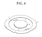
The above cutting step performed on the semiconductor wafer 2 is followed by a protective-member placing step in which an adhesive tape T is applied as a protective member to the reverse side 2 b of the semiconductor wafer 2. Specifically, as shown in FIG. 4 , the semiconductor wafer 2, i.e., the reverse side 2 b of the semiconductor wafer 2, is applied to a face side of the adhesive tape T that serves as the protective member whose outer peripheral portion is mounted on an annular frame F so that the adhesive tape T covers the inner opening of the annular frame F. The protective-member placing step is now finished. The bonded wafer W applied to the adhesive tape T has its supporting substrate 3 facing upwardly.
(Bonding-material Breaking Step)
When the protective-member placing step has been finished, a bonding-material breaking step is performed using a laser processing apparatus provided with laser beam applying means 6 as shown in FIG. 5A . The laser processing apparatus may be of known nature and its overall structure and details thereof will not be described below as it has no direct bearing on the present invention.
In preparation for the bonding-material breaking step shown in FIGS. 5A and 5B , the adhesive tape T of the bonded wafer W after performing the protective-member placing step is placed on a chuck table, not shown, of the laser processing apparatus. Suction means, not shown, is actuated to hold the bonded wafer W under suction on the chuck table through the adhesive tape T (wafer holding step). Although not shown in FIG. 5A , the annular frame F is held by an appropriate frame holding member disposed on the chuck table.
After the wafer holding step has been carried out as described above, the chuck table on which the bonded wafer W is held under suction is moved to a processing area where it is positioned directly below a beam condenser 61 of the laser beam applying means 6, as shown in FIG. 5A . Then, as shown in FIG. 5B , the laser beam applying means 6 is energized by a control signal from control means, not shown, to irradiate the bonding material B which bonds the supporting substrate 3 and the semiconductor wafer 2, from the side of the supporting substrate 3 of the bonded wafer W, with a pulsed laser beam having a wavelength which can transmit the supporting substrate 3 made of sapphire, for example, and which can be absorbed by the bonding material B made of epoxy resin, for example, thereby breaking the bonding material B. While the bonding material B is being thus irradiated with the pulsed laser beam, the chuck table is moved in the processing-feed direction indicated by an arrow X and in the indexing-feed direction indicated by an arrow Y, so that the focused spot of the pulsed laser beam emitted from the beam condenser 61 is controlled so as to be applied to the entire bonded surfaces of the semiconductor wafer 2 and supporting substrate 3 of the bonded wafer W (laser beam applying step). As a result, the bonding material B interposed between and bonding the semiconductor wafer 2 and the supporting substrate 3 is broken in its entirety, losing its bonding function to bond the semiconductor wafer 2 and the supporting substrate 3. The bonding-material breaking step is now finished.
Processing conditions in the laser beam applying step are given as follows, for example:
Light source: YAG laser
Wavelength: 355 nm
Repetition frequency: 50 kHz
Power: 0.2 W
Spot diameter: 50 μm
Pulse width: 10 ns
Feed speed: 2000 mm/second
(Supporting-substrate Peeling Step)
The bonding-material breaking step is followed by a supporting-substrate peeling step wherein the supporting substrate 3 is peeled off from the semiconductor wafer 2, separating the semiconductor wafer 2 into chips that carry the individual devices 22 thereon (see FIG. 6 ). When the bonding-material breaking step is finished, the chuck table on which the bonded wafer W is placed is moved to a peel-off position where a peeling mechanism 7 is disposed. In the peel-off position, the bonded wafer W held on the chuck table is positioned immediately below suction means 71 supported on support means 72 and the suction means 71 is lowered. Suction pads 712 a through 712 c supported through a suction passage 711 of the suction means 71 by the support means 72 are brought into contact with the supporting substrate 3. When the suction pads 712 a through 712 c contact the supporting substrate 3, suction means, not shown, is actuated to apply a negative pressure through the support means 72 and the suction passage 711 to the suction pads 712 a through 712 c, which attract the supporting substrate 3 under suction. When the suction pads 712 a through 712 c attract the supporting substrate 3 under suction, the suction pads 712 a through 712 c which are attracting the supporting substrate 3 under suction are moved upwardly away from the bonded wafer W, as shown in FIG. 6 , thereby peeling the supporting substrate 3 off from the semiconductor wafer 2. The supporting-substrate peeling step is now finished. When the supporting-substrate peeling step is finished, the supporting substrate 3 which has been peeled off is housed in a supporting substrate container, not shown. The devices 22 which have been bonded to the supporting substrate 3 are now individually separately held on the adhesive tape T placed on the chuck table.
(Pickup Step)
After the supporting-substrate peeling step is finished, a pickup step is performed to pick up the devices 22 from the adhesive tape T. The pickup step is carried out by a pickup apparatus 8 which is fragmentarily shown in FIG. 7 . The pickup apparatus 8 includes a frame holding member 81, a plurality of clamps 82 mounted on the frame holding member 81 for holding the annular frame F placed on an upper surface of the frame holding member 81, and an expanding drum 83 in the form of a hollow cylinder that is open in at least an upper end thereof, for expanding the adhesive tape T mounted on the annular frame F held in position by the clamps 82, with the individual devices 22 supported on the upper surface of the adhesive tape T. The frame holding member 81 is vertically movably supported by support means 823 which includes a plurality of air cylinders 823 a disposed around the expanding drum 83 and a plurality of piston rods 823 b extending upwardly from the respective air cylinders 823 a.
The expanding drum 83 is of a diameter smaller than the inside diameter of the annular frame F and greater than the outside diameter of the semiconductor wafer 2 applied to the adhesive tape T mounted on the annular frame F. As shown in FIG. 7 , the pickup apparatus 8 can selectively take a position, indicated by the dotted lines, where the frame holding member 81 and the upper end of the expanding drum 83 lie flush with each other and a position, indicated by the solid lines, where the frame holding member 81 is lowered by the support means 823 to make the upper end of the expanding drum 83 higher than the upper end of the frame holding member 81.
When the frame holding member 81 is lowered by the support means 823 to relatively change the upper end of the expanding drum 83 from the dotted-line position to the solid-line position where the upper end of the expanding drum 83 is higher than the upper end of the frame holding member 81, the adhesive tape T mounted on the annular frame F is expanded radially outwardly by contact with the upper end of the expanding drum 83. As a result, a tensile force is applied radially outwardly to the semiconductor wafer 2 applied to the adhesive tape T, spreading the intervals between the individual devices 22 that have already been separated. Then, a pickup collet 84 is actuated to pick up the devices 22, thus spaced apart, one by one off from the adhesive tape T, and carries them to a container tray, not shown. The pickup step is now finished, bringing an end to the method of processing a wafer according to the present invention. According to the present embodiment, the bonding material B is also cut as well as the semiconductor wafer 2 in the cutting step. However, the present invention is not limited to such cutting details. If the bonding material B is not fully severed, but remains uncut in the cutting step, then it is fully separated when the adhesive tape T is expanded in the pickup step.
With the above arrangement of the present invention, before the cut grooves are formed in the wafer along the division lines, the reverse side of the wafer is ground while the face side thereof is being supported by the supporting substrate. Therefore, since no individual devices are scattered or broken in the reverse-side grinding step, the present invention is advantageous in that smaller or thinner device chips which are of a square shape as small as 1 mm on each side or of a thickness of 10 μm or less can be manufactured with ease.
In the above embodiment, the cutting blade is used as specific means for carrying out the cutting step to form cut grooves along the division lines. However, the present invention is not limited to using the cutting blade. The means for forming cut grooves may be any of various cutting means such as a laser beam, plasma etching, wet etching, etc.
In the protective-member placing step according to the above embodiment, the wafer is placed in the opening of the annular frame, and the reverse side of the wafer and the outer periphery of the annular frame are joined to each other by the adhesive tape, so that the adhesive tape is placed as the protective member on the reverse side of the wafer by supporting the wafer on the annular frame. However, the present invention is not limited to such details of the protective-member placing step. A tape serving as a protective member that is identical in shape to the wafer may be applied to the reverse side of the wafer, or the face side of the wafer may be coated with a resin layer serving as a protective member.
In the above embodiment, the reverse-side grinding step is immediately followed by the cutting step. However, if the devices to be manufactured formed on the wafer are power devices, then a step of forming electrodes on the reverse side of the wafer is added between the reverse-side grinding step and the cutting step.
The present invention is not limited to the details of the above described preferred embodiment. The scope of the invention is defined by the appended claims and all changes and modifications as fall within the equivalence of the scope of the claims are therefore to be embraced by the invention.
Claims (3)
1. A method of processing a wafer by dividing a wafer with devices formed on areas on a face side thereof which are demarcated by a plurality of division lines, along the division lines into chips that carry the individual devices thereon, the method comprising:
an integrating step of placing a supporting substrate in confronting relation to the face side of the wafer and integrally bonding the supporting substrate to the face side of the wafer with a bonding material; followed by the step of
a reverse-side grinding step of grinding a reverse side of the wafer to thin the wafer after performing the integrating step; followed by the step of
a cutting step of cutting the wafer along the division lines from the ground reverse side of the wafer into the chips that carry the individual devices thereon; followed by the step of
a protective-member placing step of placing a protective member on the reverse side of the wafer which has been cut along the division lines; followed by the step of
a bonding-material breaking step of applying a laser beam having a wavelength which is able to transmit the supporting substrate in a condition where a focused spot of the laser beam is set in the bonding material, thereby breaking the bonding material; followed by the step of
a supporting-substrate peeling step of peeling the supporting substrate off from the devices to separate the chips that carry the individual devices thereon.
2. The method of processing a wafer according to claim 1 , wherein, in the protective-member placing step, the wafer is placed in an opening of a frame and the reverse side of the wafer and an inner periphery of the frame are joined to each other by an adhesive tape, so that the adhesive tape is placed as the protective member on the reverse side of the wafer by supporting the wafer on the frame, the method further comprising
a pickup step of expanding the adhesive tape to expand intervals between the devices, and picking up the devices from the adhesive tape after performing the supporting-substrate peeling step.
3. The method of processing a wafer according to claim 1 , wherein the cutting step includes any one of a cutting step using a cutting blade, a cutting step using a laser beam, a cutting step using plasma etching, and a cutting step using wet etching.
Applications Claiming Priority (2)
| Application Number | Priority Date | Filing Date | Title |
|---|---|---|---|
| JP2015237184A JP2017103406A (en) | 2015-12-04 | 2015-12-04 | Wafer processing method |
| JP2015-237184 | 2015-12-04 |
Publications (2)
| Publication Number | Publication Date |
|---|---|
| US20170162420A1 US20170162420A1 (en) | 2017-06-08 |
| US10083849B2 true US10083849B2 (en) | 2018-09-25 |
Family
ID=58722539
Family Applications (1)
| Application Number | Title | Priority Date | Filing Date |
|---|---|---|---|
| US15/367,558 Active 2036-12-11 US10083849B2 (en) | 2015-12-04 | 2016-12-02 | Method of processing wafer |
Country Status (6)
| Country | Link |
|---|---|
| US (1) | US10083849B2 (en) |
| JP (1) | JP2017103406A (en) |
| KR (1) | KR20170066251A (en) |
| CN (1) | CN107039341A (en) |
| DE (1) | DE102016224033A1 (en) |
| TW (1) | TWI703625B (en) |
Families Citing this family (6)
| Publication number | Priority date | Publication date | Assignee | Title |
|---|---|---|---|---|
| JP6980421B2 (en) * | 2017-06-16 | 2021-12-15 | 株式会社ディスコ | Wafer processing method |
| CN107733389B (en) * | 2017-11-01 | 2020-12-01 | 深圳市深汕特别合作区应达利电子科技有限公司 | Quartz crystal large wafer and method for manufacturing small wafer by using same |
| JP6991673B2 (en) * | 2018-02-27 | 2022-01-12 | 株式会社ディスコ | Peeling method |
| JP7201342B2 (en) * | 2018-06-06 | 2023-01-10 | 株式会社ディスコ | Wafer processing method |
| CN109746796A (en) * | 2019-01-10 | 2019-05-14 | 湘潭大学 | A kind of dicing device and method for SiC wafer |
| TWI783395B (en) * | 2021-03-03 | 2022-11-11 | 華泰電子股份有限公司 | Wafer thinning method |
Citations (4)
| Publication number | Priority date | Publication date | Assignee | Title |
|---|---|---|---|---|
| JPH1140520A (en) | 1997-07-23 | 1999-02-12 | Toshiba Corp | Method of dividing wafer and manufacture of semiconductor device |
| US20070298587A1 (en) * | 2004-03-29 | 2007-12-27 | J.P. Sercel Associates Inc. | Method of separating layers of material |
| US20110241178A1 (en) * | 2010-04-01 | 2011-10-06 | Panasonic Corporation | Semiconductor device and method of manufacturing the same |
| US8048780B2 (en) * | 2008-08-12 | 2011-11-01 | Disco Corporation | Method of processing optical device wafer |
Family Cites Families (7)
| Publication number | Priority date | Publication date | Assignee | Title |
|---|---|---|---|---|
| TWI267913B (en) * | 2005-09-23 | 2006-12-01 | Advanced Semiconductor Eng | Wafer dicing method |
| JP2011187479A (en) * | 2010-03-04 | 2011-09-22 | Disco Corp | Wafer processing method |
| JP2011253939A (en) * | 2010-06-02 | 2011-12-15 | Sony Chemical & Information Device Corp | Wafer dicing method, connecting method, connecting structure |
| JP5580800B2 (en) * | 2010-10-29 | 2014-08-27 | 東京応化工業株式会社 | Laminated body and method for separating the laminated body |
| US8999768B2 (en) * | 2011-03-14 | 2015-04-07 | Fuji Electric Co., Ltd. | Semiconductor device manufacturing method |
| JP5911750B2 (en) * | 2012-05-14 | 2016-04-27 | アルバック成膜株式会社 | Wafer support and manufacturing method thereof |
| JP6215544B2 (en) * | 2013-03-18 | 2017-10-18 | 株式会社ディスコ | Wafer processing method |
-
2015
- 2015-12-04 JP JP2015237184A patent/JP2017103406A/en active Pending
-
2016
- 2016-10-27 TW TW105134772A patent/TWI703625B/en active
- 2016-11-30 CN CN201611079386.5A patent/CN107039341A/en active Pending
- 2016-11-30 KR KR1020160161428A patent/KR20170066251A/en not_active Application Discontinuation
- 2016-12-02 US US15/367,558 patent/US10083849B2/en active Active
- 2016-12-02 DE DE102016224033.1A patent/DE102016224033A1/en active Granted
Patent Citations (4)
| Publication number | Priority date | Publication date | Assignee | Title |
|---|---|---|---|---|
| JPH1140520A (en) | 1997-07-23 | 1999-02-12 | Toshiba Corp | Method of dividing wafer and manufacture of semiconductor device |
| US20070298587A1 (en) * | 2004-03-29 | 2007-12-27 | J.P. Sercel Associates Inc. | Method of separating layers of material |
| US8048780B2 (en) * | 2008-08-12 | 2011-11-01 | Disco Corporation | Method of processing optical device wafer |
| US20110241178A1 (en) * | 2010-04-01 | 2011-10-06 | Panasonic Corporation | Semiconductor device and method of manufacturing the same |
Also Published As
| Publication number | Publication date |
|---|---|
| JP2017103406A (en) | 2017-06-08 |
| US20170162420A1 (en) | 2017-06-08 |
| CN107039341A (en) | 2017-08-11 |
| TWI703625B (en) | 2020-09-01 |
| DE102016224033A1 (en) | 2017-06-08 |
| TW201724244A (en) | 2017-07-01 |
| KR20170066251A (en) | 2017-06-14 |
Similar Documents
| Publication | Publication Date | Title |
|---|---|---|
| US10083849B2 (en) | Method of processing wafer | |
| US9685377B2 (en) | Wafer processing method | |
| TWI650809B (en) | Wafer processing method | |
| TWI438834B (en) | Method of dividing an adhesive film bonded to a wafer | |
| US7888239B2 (en) | Semiconductor device manufacturing method | |
| US7915140B2 (en) | Fabrication method for device having die attach film on the back side thereof | |
| US7622366B2 (en) | Method of manufacturing semiconductor device | |
| US9779993B2 (en) | Wafer processing method including attaching a protective tape to a front side of a functional layer to prevent debris adhesion | |
| TWI704609B (en) | Wafer processing method | |
| US9735040B2 (en) | Method of processing single-crystal substrate | |
| TWI665720B (en) | Processing method of wafer | |
| US20070128834A1 (en) | Wafer dividing method | |
| KR101938426B1 (en) | Forming method of chip with die attach film | |
| US9627242B2 (en) | Wafer processing method | |
| US9543466B2 (en) | Method for forming shield tunnels in single-crystal substrates | |
| US10985065B2 (en) | Method of dicing a wafer by pre-sawing and subsequent laser cutting | |
| US10103061B2 (en) | Processing method of single-crystal substrate | |
| US9698301B2 (en) | Wafer processing method | |
| US10157793B2 (en) | Method of processing single-crystal substrate | |
| KR20180048376A (en) | Method for processing wafer | |
| JP4768963B2 (en) | Wafer transfer method | |
| CN107799406B (en) | Method for processing wafer and method for processing carrier | |
| US20240128087A1 (en) | Wafer processing method | |
| TW201503253A (en) | Processing method of wafer | |
| JP2022054894A (en) | Wafer processing method |
Legal Events
| Date | Code | Title | Description |
|---|---|---|---|
| AS | Assignment |
Owner name: DISCO CORPORATION, JAPAN Free format text: ASSIGNMENT OF ASSIGNORS INTEREST;ASSIGNOR:MORIKAZU, HIROSHI;REEL/FRAME:040495/0482 Effective date: 20161107 |
|
| STCF | Information on status: patent grant |
Free format text: PATENTED CASE |
|
| MAFP | Maintenance fee payment |
Free format text: PAYMENT OF MAINTENANCE FEE, 4TH YEAR, LARGE ENTITY (ORIGINAL EVENT CODE: M1551); ENTITY STATUS OF PATENT OWNER: LARGE ENTITY Year of fee payment: 4 |