US10082905B2 - Touch control display panel and touch control display device - Google Patents
Touch control display panel and touch control display device Download PDFInfo
- Publication number
- US10082905B2 US10082905B2 US15/452,774 US201715452774A US10082905B2 US 10082905 B2 US10082905 B2 US 10082905B2 US 201715452774 A US201715452774 A US 201715452774A US 10082905 B2 US10082905 B2 US 10082905B2
- Authority
- US
- United States
- Prior art keywords
- touch
- electrically connected
- touch signal
- signal control
- display panel
- Prior art date
- Legal status (The legal status is an assumption and is not a legal conclusion. Google has not performed a legal analysis and makes no representation as to the accuracy of the status listed.)
- Active
Links
Images


Classifications
-
- G—PHYSICS
- G06—COMPUTING OR CALCULATING; COUNTING
- G06F—ELECTRIC DIGITAL DATA PROCESSING
- G06F3/00—Input arrangements for transferring data to be processed into a form capable of being handled by the computer; Output arrangements for transferring data from processing unit to output unit, e.g. interface arrangements
- G06F3/01—Input arrangements or combined input and output arrangements for interaction between user and computer
- G06F3/03—Arrangements for converting the position or the displacement of a member into a coded form
- G06F3/041—Digitisers, e.g. for touch screens or touch pads, characterised by the transducing means
- G06F3/0412—Digitisers structurally integrated in a display
-
- G—PHYSICS
- G06—COMPUTING OR CALCULATING; COUNTING
- G06F—ELECTRIC DIGITAL DATA PROCESSING
- G06F3/00—Input arrangements for transferring data to be processed into a form capable of being handled by the computer; Output arrangements for transferring data from processing unit to output unit, e.g. interface arrangements
- G06F3/01—Input arrangements or combined input and output arrangements for interaction between user and computer
- G06F3/03—Arrangements for converting the position or the displacement of a member into a coded form
- G06F3/041—Digitisers, e.g. for touch screens or touch pads, characterised by the transducing means
- G06F3/0416—Control or interface arrangements specially adapted for digitisers
- G06F3/04164—Connections between sensors and controllers, e.g. routing lines between electrodes and connection pads
-
- G—PHYSICS
- G06—COMPUTING OR CALCULATING; COUNTING
- G06F—ELECTRIC DIGITAL DATA PROCESSING
- G06F3/00—Input arrangements for transferring data to be processed into a form capable of being handled by the computer; Output arrangements for transferring data from processing unit to output unit, e.g. interface arrangements
- G06F3/01—Input arrangements or combined input and output arrangements for interaction between user and computer
- G06F3/03—Arrangements for converting the position or the displacement of a member into a coded form
- G06F3/041—Digitisers, e.g. for touch screens or touch pads, characterised by the transducing means
- G06F3/0416—Control or interface arrangements specially adapted for digitisers
- G06F3/0418—Control or interface arrangements specially adapted for digitisers for error correction or compensation, e.g. based on parallax, calibration or alignment
- G06F3/04184—Synchronisation with the driving of the display or the backlighting unit to avoid interferences generated internally
-
- G—PHYSICS
- G06—COMPUTING OR CALCULATING; COUNTING
- G06F—ELECTRIC DIGITAL DATA PROCESSING
- G06F3/00—Input arrangements for transferring data to be processed into a form capable of being handled by the computer; Output arrangements for transferring data from processing unit to output unit, e.g. interface arrangements
- G06F3/01—Input arrangements or combined input and output arrangements for interaction between user and computer
- G06F3/03—Arrangements for converting the position or the displacement of a member into a coded form
- G06F3/041—Digitisers, e.g. for touch screens or touch pads, characterised by the transducing means
- G06F3/044—Digitisers, e.g. for touch screens or touch pads, characterised by the transducing means by capacitive means
- G06F3/0445—Digitisers, e.g. for touch screens or touch pads, characterised by the transducing means by capacitive means using two or more layers of sensing electrodes, e.g. using two layers of electrodes separated by a dielectric layer
-
- G—PHYSICS
- G06—COMPUTING OR CALCULATING; COUNTING
- G06F—ELECTRIC DIGITAL DATA PROCESSING
- G06F3/00—Input arrangements for transferring data to be processed into a form capable of being handled by the computer; Output arrangements for transferring data from processing unit to output unit, e.g. interface arrangements
- G06F3/01—Input arrangements or combined input and output arrangements for interaction between user and computer
- G06F3/03—Arrangements for converting the position or the displacement of a member into a coded form
- G06F3/041—Digitisers, e.g. for touch screens or touch pads, characterised by the transducing means
- G06F3/044—Digitisers, e.g. for touch screens or touch pads, characterised by the transducing means by capacitive means
- G06F3/0446—Digitisers, e.g. for touch screens or touch pads, characterised by the transducing means by capacitive means using a grid-like structure of electrodes in at least two directions, e.g. using row and column electrodes
-
- G—PHYSICS
- G09—EDUCATION; CRYPTOGRAPHY; DISPLAY; ADVERTISING; SEALS
- G09G—ARRANGEMENTS OR CIRCUITS FOR CONTROL OF INDICATING DEVICES USING STATIC MEANS TO PRESENT VARIABLE INFORMATION
- G09G2310/00—Command of the display device
- G09G2310/02—Addressing, scanning or driving the display screen or processing steps related thereto
- G09G2310/0264—Details of driving circuits
- G09G2310/0286—Details of a shift registers arranged for use in a driving circuit
-
- G—PHYSICS
- G09—EDUCATION; CRYPTOGRAPHY; DISPLAY; ADVERTISING; SEALS
- G09G—ARRANGEMENTS OR CIRCUITS FOR CONTROL OF INDICATING DEVICES USING STATIC MEANS TO PRESENT VARIABLE INFORMATION
- G09G3/00—Control arrangements or circuits, of interest only in connection with visual indicators other than cathode-ray tubes
- G09G3/20—Control arrangements or circuits, of interest only in connection with visual indicators other than cathode-ray tubes for presentation of an assembly of a number of characters, e.g. a page, by composing the assembly by combination of individual elements arranged in a matrix no fixed position being assigned to or needed to be assigned to the individual characters or partial characters
-
- G—PHYSICS
- G11—INFORMATION STORAGE
- G11C—STATIC STORES
- G11C19/00—Digital stores in which the information is moved stepwise, e.g. shift registers
Definitions
- the present disclosure generally relates to the field of display technology and, more specifically, relates to a touch control display panel and a touch control display device thereof.
- Touch control display devices are able to detect the coordinates of the position on a touchscreen contacted by a finger, stylus, or other objects, and display corresponding information according to the detected coordinates.
- a current touch control display panel often includes two touch control electrode layers, each of which includes a plurality of touch control electrodes arranged in parallel. The touch control electrodes in one touch control electrode layer intersect the touch control electrodes in the other touch control electrode layer. Capacitors are formed in intersections between the touch control electrodes in the two touch control electrode layers.
- each touch control electrode i.e., touch driving electrode
- the touchscreen is pressed or tapped by the finger
- a capacitance change is introduced, and an electrical current is generated accordingly.
- a touch sensing circuit identifies two perpendicular touch control electrodes where the capacitance changes and, thus, determines the point at which the touch occurs.
- an integrated circuit (IC) of the touch control display device sequentially applies touch driving signals to the touch driving electrodes.
- a touch shift register circuit which provides touch driving signals in sequence to the touch driving electrodes, is often disposed at the bottom of the touch control display panel.
- the IC may input the touch driving signal to the touch shift register circuit through one output terminal. Then the touch shift register circuit sequentially shifts the touch driving signal and output the shifted touch driving signal to the corresponding touch driving electrode.
- the touch shift register circuit may include a substantially large number of components/elements, which occupy a substantially large space in the display panel and, accordingly, bring challenges to realize a narrow frame of the display panel.
- the disclosed touch control display panel and touch control display device thereof are directed to solve one or more problems set forth above and other problems.
- the touch control display panel comprises a plurality of scanning lines; a plurality of data lines; a pixel array confined by the scanning lines and the data lines; a shift register including a plurality of cascaded shift register units; a touch driving electrode array including a plurality of touch driving electrodes; a touch switching control circuit and a plurality of touch signal lines; and a touch signal control line cluster including a plurality of touch signal control lines.
- the scanning lines are extending in a first direction.
- the data lines are extending in a second direction and intersecting the scanning lines.
- a scanning line is electrically connected to an output terminal of a shift register unit.
- a touch signal line has one end electrically connected to a touch driving electrode, and the other end electrically connected to an output terminal of the touch switching control circuit.
- a touch signal control line has one end electrically connected to the output terminal of the shift register unit, and the other end electrically connected to the touch switching control circuit. The touch switching control circuit is controlled by the touch signal control line to provide a touch driving signal to the touch signal line.
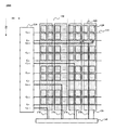
- FIG. 1 illustrates a schematic diagram of an exemplary touch control display panel consistent with disclosed embodiments
- FIG. 2 illustrates a schematic diagram of an exemplary touch signal control line in an exemplary touch control display panel consistent with disclosed embodiments
- FIG. 3A illustrates an A-A′ cross sectional view of an exemplary touch control display panel in FIG. 1 having an exemplary touch signal control line with a first segment and a second segment disposed in different conductive layers consistent with disclosed embodiments;
- FIG. 3B illustrates an A-A′ cross sectional view of an exemplary touch control display panel in FIG. 1 having an exemplary touch signal control line with a first segment and a second segment disposed in a same conductive layer consistent with disclosed embodiments;
- FIG. 4 illustrates a schematic diagram of another exemplary touch control display panel consistent with disclosed embodiments
- FIG. 5 illustrates a schematic diagram of an exemplary touch signal control line corresponding to an exemplary touch driving electrode consistent with disclosed embodiments in FIG. 4 ;
- FIG. 6A illustrates an equivalent circuit diagram of an exemplary touch switching control circuit consistent with disclosed embodiments
- FIG. 6B illustrates a schematic diagram of an exemplary touch control display panel having an exemplary touch switching control circuit in FIG. 6A consistent with disclosed embodiments
- FIG. 7A illustrates an equivalent circuit diagram of another exemplary touch switching control circuit consistent with disclosed embodiments
- FIG. 7B illustrates a schematic diagram of an exemplary touch control display panel having an exemplary touch switching control circuit in FIG. 7A consistent with disclosed embodiments
- FIG. 8 illustrates an exemplary timing diagram for driving an exemplary touch control display panel in FIG. 7B consistent with disclosed embodiments
- FIG. 9 illustrates a schematic diagram of another exemplary touch control display panel consistent with disclosed embodiments.
- FIG. 10 illustrates an exemplary touch control display panel consistent with disclosed embodiments.
- FIG. 11 illustrates an exemplary touch control display device consistent with disclosed embodiments.
- the present disclosure provides an improved touch control display panel capable of reducing the number of the terminals for outputting the touch driving signals and simplifying the integrated circuit (IC), thereby narrowing the frame of the touch control display panel.
- IC integrated circuit
- FIG. 1 illustrates a schematic diagram of an exemplary touch control display panel consistent with disclosed embodiments.
- the touch control display panel may be a liquid crystal display (LCD) touch control display panel, an organic light-emitting diode (OLED) touch control display panel, a plasma touch control display panel (PDP), a field emission touch control display (FED) panel, a light-emitting diode (LED) touch control display panel, a quantum dots (QDs) touch control display panel, an electrophoretic touch control display panel or other appropriate touch control display panel capable of displaying videos and/or images.
- LCD liquid crystal display
- OLED organic light-emitting diode
- PDP plasma touch control display panel
- FED field emission touch control display
- LED light-emitting diode
- QDs quantum dots
- the touch control display panel 1000 may include m number of scanning lines 110 and n number of data lines 190 , where m and n are positive integers.
- the scanning lines 110 and the data lines 190 may extend along a first direction D 1 and a second direction D 2 , respectively.
- the second direction D 2 may intersect the first direction D 1 .
- the scanning lines 110 may intersect the data lines 190 to confine a pixel array, which may include a plurality of display pixels 120 arranged in an array.
- the first direction D 1 and the second direction D 2 in FIG. 1 are for illustrative purposes and are not intended to limit the scope of the present disclosure.
- the touch control display panel 1000 may also include a shift register 130 including a plurality of cascaded shift register units. Each scanning line 110 may be electrically connected to an output terminal of a corresponding shift register unit.
- the touch control display panel 1000 may also include a touch switching control circuit 140 , a plurality of touch signal lines 150 , and a touch driving electrode array including k number of touch driving electrodes 160 .
- Each touch signal line 150 may have one end electrically connected to a corresponding touch driving electrode 160 , and the other end electrically connected to an output terminal of the touch switching control circuit 140 .
- control display panel 1000 may also include a touch signal control line cluster.
- the touch signal control line cluster may include a plurality of touch signal control lines.
- Each touch signal control line 170 may have one end electrically connected to an output terminal of a corresponding shift register unit, and the other end electrically connected to an output terminal of the touch switching control circuit 140 .
- the touch switching control circuit 140 may provide a touch driving signal to each touch signal line 150 .
- One of touch signal control lines 170 may be electrically connected to an output terminal G i1+1 of the (i1+1)-th stage shift register unit. That is, with the step-by-step output of the shift register 130 , when the (i1+1)-th stage shift register unit outputs a signal, the touch signal control line 170 electrically connected to the output terminal of the (i1+1)-th stage shift register unit may control the touch switching control circuit 140 to output a touch diving signal to the touch signal line 150 controlled by the touch signal control line 170 .
- touch signal control lines 170 which control different touch signal lines 150 , are connected to different shift register units in the shift register 130 , two different touch driving electrodes 160 may not simultaneously receive the touch driving signal. Thus, a sequential scanning over each touch driving electrode 160 may be realized.
- the touch switching control circuit 140 including fewer electrical elements may be disposed in the touch control display panel, thereby simplifying the circuits in touch control display panels and realizing the sequential scanning over each touch driving electrode 160 .
- FIG. 1 shows that the shift register 130 is disposed at one side of the touch control display panel 1000 , which is for illustrative purposes and is not intended to limit the scope of the present disclosure.
- the shift register 130 inducing a plurality of shift register units may be disposed at different sides of the touch control display panel according to various application scenarios.
- the shift register 130 inducing a plurality of shift register units may be disposed at one side of the touch control display panel.
- some shift register units may be disposed at one side of the touch control display panel, and some shift register units may be disposed at another side of the touch control display panel.
- the number of the shift register units disposed at each side of the touch control display panel may be reduced and, accordingly, the size of the frame may be reduced. That is, a narrow frame of the touch control display panel may be realized.
- the touch control display panel 1000 may comprise a first conductive layer, a second conductive layer, and a first insulating layer.
- the first insulating layer may be formed between the first conductive layer and the second conductive layer.
- the scanning lines 110 may be formed on the first conductive layer, while the data lines 190 may be formed on the second conductive layer.
- FIG. 2 illustrates a schematic diagram of an exemplary touch signal control line in an exemplary touch control display panel consistent with disclosed embodiments.
- the touch signal control line 170 may include a first segment 171 and a second segment 172 extending in a first direction of D 1 and a second direction of D 2 , respectively.
- the first direction D 1 and the second direction D 2 in FIG. 2 are for illustrative purposes and are not intended to limit the scope of the present disclosure.
- the first segment 171 of each touch signal control line 170 may have one end electrically connected to an output terminal of one shift register unit, and the other end electrically connected to one end of the second segment 172 of the touch signal control line 170 .
- the other end of the second segment 172 may be electrically connected to the control terminal of the touch switching control circuit 140
- a signal outputted from the output terminal of the shift register unit may be transmitted through the first segment 171 and the second segment 172 of the touch signal control line 170 to the touch switching control circuit 140 , thereby controlling the touch switching control circuit 140 to output the touch driving signal to the corresponding touch signal line 150 .
- first segment 171 and the second segment 172 of the touch signal control line 170 may be formed in the first conductive layer and the second conductive layer, respectively.
- the first segment 171 of the touch signal control line 170 may be electrically connected to the second segment 172 of the same touch signal control line 170 via a through-hole formed in the first insulating layer.
- the first segment 171 of the touch signal control line 170 may be disposed at the same layer as the scanning line 110 of the touch control display panel 1000
- the second segment 172 of the touch signal control lines 170 may be disposed at the same layer as the data lines of the touch control display panel 1000
- the touch signal control lines 170 may be disposed on the existing conductive layers of the touch control display panel 1000 without introducing extra conductive layers, thereby eliminating the possibility of increasing the thickness of the touch control display panel due to the introduction of the touch signal control lines 170 .
- the corresponding structure is shown in FIG. 3A .
- FIG. 3A illustrates an A-A′ cross sectional view of an exemplary touch control display panel in FIG. 1 having an exemplary touch signal control line with a first segment and a second segment disposed in different conductive layers consistent with disclosed embodiments. Note that the data lines are not shown in FIG. 3A .
- the reference numeral 160 denotes a touch driving electrode.
- the first segment 171 and the second segment 172 of the touch signal control line 170 may be formed on a first conductive layer and a second conductive layer, respectively.
- the first segment 171 and the second segment 172 may be electrically connected via a through-hole 173 in a first insulating layer, which is disposed between the first conductive layer and the second conductive layer.
- the touch control display panel may further include a third conductive layer and each touch signal control line may be formed in the third conductive layer.
- the corresponding structure is shown in FIG. 3B .
- FIG. 3B illustrates an A-A′ cross sectional view of an exemplary touch control display panel in FIG. 1 having an exemplary touch signal control line with a first segment and a second segment disposed in a same conductive layer consistent with disclosed embodiments. Note that the data lines are not shown in FIG. 3B .
- the reference numeral 160 denotes a touch driving electrode.
- the touch control display panel may further include a third conductive layer and each touch signal control line may be formed in the third conductive layer. That is, both the first segment and the second segment of the touch signal control line 170 may be formed in the same layer.
- an extra through-hole 173 as shown in FIG. 3A may not have to been formed in the first insulating layer, without increasing the complexity of the patterning process for fabricating the existing insulating layers.
- both the first segment and the second segment of the touch signal control line 170 may be formed in the same patterning process and, thus, open circuit or poor conductivity due to process deviation arising from the respective fabrication of the first segment and the second segment of the touch signal control line 170 may be prevented.
- FIG. 4 illustrates a schematic diagram of another exemplary touch control display panel consistent with disclosed embodiments. The similarities between FIG. 1 and FIG. 4 are not repeated here, while certain differences may be explained.
- the touch control display panel 4000 may include m number of scanning lines 410 and n number of data lines (not shown in FIG. 4 ), extending in a first direction D 1 and a second direction D 2 , respectively.
- the scanning lines 410 and the data lines may intersect to confine a pixel array, which may include a plurality of display pixels 420 arranged in an array.
- the touch control display panel 4000 may also include a shift register 430 , which may include a plurality of cascaded shift register units.
- Each scanning line 410 may be electrically connected to an output terminal of a corresponding shift register unit.
- the touch control display panel 4000 may also include a touch driving electrode array, a touch switching control circuit 440 , and a plurality of touch signal lines 450 .
- the touch driving electrode array may include k number of touch driving electrodes 460 .
- Each touch signal line 450 may have one end electrically connected to one touch driving electrode 460 , and the other end electrically connected to an output terminal of the touch switching control circuit 440 .
- the touch control display panel 4000 may also include a touch signal control line cluster.
- the touch signal control line cluster in FIG. 4 may include a plurality of touch signal control line groups, and each touch signal control line group may include k number of touch signal control lines 470 one-to-one corresponding to the k number of touch driving electrodes 460 .
- Each touch signal control line 470 may have one end electrically connected to an output terminal of a corresponding shift register unit, and the other end electrically connected to the touch switching control circuit 440 .
- each touch signal control line group may include k number of the touch signal control lines 470 .
- Each touch signal control line group may include a touch signal control line 470 for controlling the same touch signal line 450 .
- the times of applying the driving signal to each touch driving electrode 460 in one frame period may be equal to the number of the touch signal control line groups included in the touch signal control line cluster.
- each touch driving electrode 460 may be scanned a plurality of times in one frame period and, thus, the times of touch detection may be increased and the sensitivity of touch detection may be improved, accordingly.
- the touch signal control line cluster may include two touch signal control line groups, group I and group II. Accordingly, each touch driving electrode 460 may be scanned twice in one frame period.
- the times of touch detection may be increased to twice of the times of touch detection in the touch control display panel 1000 in FIG. 1 and, accordingly, the touch detection sensitivity of the touch control display panel 4000 may be twice as high as the touch detection sensitivity of the touch control display panel 1000 in FIG. 1 .
- the two touch signal control lines 470 corresponding to the same touch driving electrode 460 may be electrically connected to an output terminal of the i-th stage shift register unit and an output terminal of the j-th stage shift register unit, respectively, where i and j are natural numbers, and
- m may be the number of scanning lines 410 disposed on the touch control display panel 4000 , i.e., the number of pixel rows in the pixel array, and the two touch signal control lines 470 may be disposed in the two touch signal control line groups (i.e., group I and group II), respectively.
- the two scans performed on the touch driving electrode 460 in one frame period may be located in a first half and a second half of the frame period, respectively.
- the scanning period may be uniformly configured in one frame period, thereby reducing the interference between the touch scanning and the displaying.
- FIG. 5 illustrates a schematic diagram of an exemplary touch signal control line corresponding to an exemplary touch driving electrode consistent with disclosed embodiments in FIG. 4 .
- the similarities between FIG. 2 and FIG. 5 are not repeated here, while certain differences may be explained.
- 471A and 472A denote a first segment and a second segment of one touch signal control line, respectively
- 471 B and 472 B denote a first segment and a second segment of another touch signal control line, respectively
- the two touch signal control lines in FIG. 5 may be configured to control the same touch driving electrode 460 .
- the second segment 472 A of one touch signal control line and the second segment 472 B of another touch signal control line may at least partially overlap with each other.
- the patterning process for fabricating each touch signal control line may be simplified, and the yield of fabricating the touch signal control line may be improved.
- FIG. 6A illustrates an equivalent circuit diagram of an exemplary touch control switching circuit consistent with disclosed embodiments.
- the touch display panel may further include a touch driving signal terminal S 1 and the touch switching control circuit 6001 may include a plurality of first transistors M 1 .
- the first transistor M 1 may include a gate electrode, a first electrode, and a second electrode.
- the gate electrode of the first transistor M 1 may be electrically connected to one of the touch signal control lines in each touch signal control line cluster, the first electrode of the first transistor M 1 may be electrically connected to the touch signal line, and the second electrode of the first transistor M 1 may be electrically connected to the touch driving signal terminal S 1 .
- the first transistor M 1 controlled by the touch signal control line in the touch switching control circuit 6001 may be turned on, and the touch driving signal outputted by the touch driving signal terminal S 1 may be provided to the corresponding touch driving electrode.
- FIG. 6B illustrates a schematic diagram of an exemplary touch control display panel having an exemplary touch control switching circuit in FIG. 6A consistent with disclosed embodiments.
- each first transistor M 1 may be electrically connected to one of the touch signal control lines 670 in each touch signal control line cluster, the first electrode of each first transistor M 1 may be electrically connected to the corresponding touch signal line 650 , and the second electrode of each first transistor M 1 may be electrically connected to the touch driving signal terminal S 1 .
- the shift register unit which is electrically connected to the touch signal control line 670 , outputs a signal
- the first transistors M 1 electrically connected to the touch signal control line 670 may be turned on, such that the touch driving signal supplied by the touch driving signal terminal S 1 may be provide to the corresponding touch driving electrode 660 .
- FIG. 7A illustrates an equivalent circuit diagram of another exemplary touch control switching circuit consistent with disclosed embodiments. The similarities between FIG. 6A and FIG. 7A are not repeated here, while certain differences may be explained.
- the touch switching control circuit 7001 may also include a plurality of the first transistors M 1 , which may be connected in the same manner as the first transistors M 1 in the touch switching control circuit 6001 in FIG. 6A .
- the touch switching control circuit 7001 may further include a plurality of second transistors M 2 , and each second transistor M 2 may also comprise a gate electrode, a first electrode, and a second electrode.
- the touch control display panel applied with the touch switching control circuit 7001 may further include a plurality of display switching control signal terminals (not drawn in FIG. 7A ) and a common voltage signal terminal S 2 .
- the touch switching control circuit 7001 may also provide the common voltage signal, supplied by the common voltage signal terminal S 2 , to each touch signal.
- each second transistor M 2 may be electrically connected to the display switching control signal terminal, the first electrode of each second transistor M 2 may be electrically connected to the common voltage signal terminal S 2 , and the second electrode of each second transistor M 2 may be electrically connected to the first electrode of the corresponding first transistor M 1 .
- the touch driving signal supplied from the touch driving signal terminal S 1 may be outputted to the touch driving electrode, which is electrically connected to the first transistor M 1 .
- the second transistor M 2 when the second transistor M 2 is turned on, the common voltage signal supplied from the common voltage signal terminal S 2 may be outputted through the second transistor M 2 to the touch driving electrode, which is electrically connected to the second transistor M 2 .
- FIG. 7B illustrates a schematic diagram of an exemplary touch control display panel having an exemplary touch control switching circuit in FIG. 7A consistent with disclosed embodiments.
- the similarities between FIG. 6B and FIG. 7B are not repeated here, while certain differences may be explained.
- each touch driving electrode 760 may also be multiplexed as a common electrode. That is, during the touch detection stage, the touch signal control line 770 may control the first transistors M 1 to be turned on, through which the touch driving electrode 760 may receive the touch driving signal outputted by the touch driving signal terminal S 1 . On the other hand, during the display stage, each of the second transistors M 2 may be turned on, through which each touch driving electrode 760 may receive the common voltage signal outputted from the common voltage signal terminal S 2 .
- the first transistor M 1 and the second transistor M 2 which are electrically connected to the same touch driving electrode 760 , may not be turned on at the same time.
- an inverter 741 may be connected between the gate electrode of the first transistor M 1 and the gate electrode of the corresponding second transistor M 2 electrically connected to the same touch driving electrode 760 .
- the input terminal and the output terminal of the inverter 741 may be connected to the gate electrode of the first transistor M 1 and the gate electrode of the second transistor M 2 , respectively.
- the first transistor M 1 and the second transistor M 2 which are electrically connected to the same touch driving electrode 760 may be not turned on at the same time.
- the gate electrodes of the first transistor M 1 and the second transistor M 2 when one of the first transistor M 1 and the second transistor M 2 is an NMOS transistor and the other is a PMOS transistor, may be electrically connected directly.
- the first electrode M 1 and the second electrode M 2 which are electrically connected to the same touch driving electrode 760 may be not simultaneously turned on.
- FIG. 8 illustrates an exemplary timing diagram for driving an exemplary touch control display panel in FIG. 7B consistent with disclosed embodiments.
- a high level signal may be received by a touch signal control line 770 which is electrically connected to the output terminal G i1+1 of the (i1+1)-th stage shift register unit of the shift register.
- the first transistor M 1 electrically connected to the touch signal control line 770 may be turned on and, accordingly, the touch driving signal outputted from the touch driving signal terminal S 1 may be outputted to the corresponding touch driving electrode via the corresponding touch signal line 750 .
- the touch signal control line 770 which is electrically connected to the output terminal G i1+1 of the (i1+1)-th stage shift register unit may receive the low level signal.
- the second transistor M 2 electrically connected to the touch signal control line 770 may be turned on and, accordingly, a common voltage signal outputted from the common voltage signal terminal S 2 may be provided to the corresponding touch driving electrode 760 .
- a high level signal may be received by the corresponding touch signal control lines 770 which are electrically connected to the corresponding output terminals, G i2+1 to G i4+1 , of the (i2+1)-th stage to the (i4+1)-th stage shift register units, respectively.
- the first transistor M 1 respectively electrically connected to the corresponding touch signal control line 770 may be turned on and, accordingly, the touch driving signal outputted from the touch driving signal terminal S 1 may be transmitted to the corresponding touch driving electrode 760 via the associated touch signal line 750 .
- the low level signal may be received by the corresponding touch signal control lines 770 which are electrically connected to the corresponding output terminals, G i2+1 to G i4+1 , of the (i2+1)-th stage to the (i4+1)-th stage shift register units.
- the second transistor M 2 electrically connected to the corresponding touch signal control line 770 may be turned on and, accordingly, the common voltage signal outputted from the common voltage signal terminal S 2 may be provided to the corresponding touch driving electrode 760 .
- an extra touch shift register circuit of more electrical elements may be removed from the bottom frame of touch control display panel.
- a touch switching control circuit of fewer electrical elements may be disposed in the touch control display panels to realize the sequential scanning over each touch driving electrode, thereby narrowing the frame at each side of touch control display panel.
- FIG. 9 illustrates a schematic diagram of another exemplary touch control display panel consistent with disclosed embodiments. The similarities between FIG. 1 and FIG. 9 are not repeated here, while certain differences may be explained.
- the touch control display panel 9000 may include m number of scanning lines 910 and n number of data lines (not shown in FIG. 9 ) extending in a first direction D 1 and a second direction D 2 , respectively.
- the second direction D 2 may intersect the first direction D 1 to confine a pixel array, which may include a plurality of pixels 920 arranged in an array.
- the touch control display panel 9000 may also include a shift register 930 , which may include a plurality of cascaded shift register units. Each of the scanning lines 910 may be connected to an output terminal of a corresponding shift register unit.
- the touch control display panel 9000 may also include a touch driving electrode array including k number of the touch driving electrodes 960 , a touch switching control circuit 940 , and a plurality of touch signal lines 950 .
- One end of each touch signal line 950 may be electrically connected to one of touch driving electrodes 960
- the other end of each touch signal line 950 may be electrically connected to an output terminal of the touch switching control circuit 940 .
- the touch control display panel 9000 may further include a touch signal control line cluster, which may include a plurality of touch signal control lines 970 .
- a touch signal control line cluster may include a plurality of touch signal control lines 970 .
- One end of each touch signal control line 970 may be electrically connected to an output terminal of a corresponding shift register unit, while the other end of each touch signal control line 970 may be electrically connected to an output terminal of the touch switching control circuit 940 .
- the touch switching control circuit 940 may be controlled by each touch signal control line 970 to provide the touch driving signal to each touch signal line 950 .
- the touch control display panel 9000 in FIG. 9 may further include a plurality of resistors R 1 .
- Each resistor R 1 may be connected between an output terminal of a corresponding shift register unit electrically connected to one touch signal control line 970 and the touch switching control circuit 940 .
- the signals outputted to the touch switching control circuit 940 via each touch signal control line 970 may have the same magnitude of amplitude.
- the touch control display panel 9000 through disposing a plurality of resistors R 1 with variable resistance values between the output terminals of the shift register units and the touch switching control circuit 940 , the resistance difference among different touch signal control lines 970 with various lengths may be eliminated.
- a resistor R 1 with smaller resistance may be provided to a longer touch signal control line 970 , while a resistor R 1 with larger resistance may be provided to a shorter touch signal control line 970 .
- the control signals passing through different touch signal control lines 970 into the touch switching control circuit 940 may have the same magnitude of amplitude.
- FIG. 9 illustrates each resistor R 1 is disposed between the touch signal control line 970 and the touch switching control circuit 940 , which is for illustrative purposes and is not intended to limit the scope of the present disclosure.
- the resistor R 1 may be positioned at various places in the touch control display panel 9000 according to various application scenarios, as long as the resistance of resistor R 1 may be varied to enable the input signals into the touch switching control circuit 940 to have the same magnitude of amplitude.
- the resistor R 1 may be disposed at the output terminal of the shift register unit which is electrically connected to the corresponding touch signal control line 970 .
- the touch control display panel may include a display area and a non-display area surrounding the display area.
- the non-display area may include a first frame region, and a second frame region connecting the first frame region.
- the shift register and the touch switching control circuit may be formed in the first frame region and the second frame region, respectively.
- the first frame region may be the left-side frame or the right-side frame of the touch control display panel
- the second frame region may be the bottom-side frame of the touch control display panel
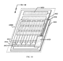
- FIG. 10 illustrates an exemplary touch control display panel consistent with disclosed embodiments.
- the touch control display panel 10000 may include an array substrate 1010 and a color film substrate 1020 disposed opposite to the array substrate 1010 .
- a plurality of touch driving electrodes 1011 arranged in an array may be disposed on the array substrate 1010 .
- a plurality of touch sensing electrodes 1021 arranged in an array may be disposed on the color film substrate 1020 .
- the touch driving electrode 1011 may be a striped electrode extending in the direction of D 2
- the touch sensing electrode 1021 may also be a striped electrode extending in the direction of D 1 .
- the orthogonal projection of each touch sensing electrode 1021 onto the array of touch driving electrodes 1011 may partially overlap with the respective touch driving electrode 1011 .
- the shape of the touch driving electrode 1011 and the touch sensing electrode 1021 is for illustrative purposes and is not intended to limit the scope of the present disclosure.
- the touch sensing electrode array may be disposed on the surface of the color film substrate 1020 far away from the array substrate 1010 .
- the touch sensing electrode array may be disposed on the top surface of the color film substrate 1020 .
- the touch driving electrode array may be disposed on the surface of the array substrate 1010 facing towards the color film substrate 1020 .
- the touch control display panel 10000 may further include an integrated circuit 1012 , a plurality of touch signal lines 1013 , and a plurality of touch sensing signal lines 1022 .
- Each touch signal line 1013 may have one end connected to the corresponding touch driving electrode 1011 , and the other end connected to the integrated circuit 1012 .
- each touch sensing signal line 1022 may have one end connected to the corresponding touch sensing electrode 1021 , and the other end connected to the integrated circuit 1012 .
- a flexible printed circuit board may be adopted to connect the touch sensing signal lines 1022 and the integrated circuit 1012 .
- the integrated circuit 1012 may provide the touch scan signal to each touch driving electrode 1011 and, meanwhile, receive the touch sensing signal from each touch sensing electrode 1021 .
- the integrated circuit 1012 in the touch stage may provide the touch scan signals in sequence to each touch driving electrode 1011 and, meanwhile, may receive the touch sensing signals from all the touch sensing electrodes 1021 .
- the touch position may be determined by distinguishing the difference in the touch sensing signals transmitted by the touch sensing electrodes 1021 .
- each touch driving electrode 1011 may be multiplexed as a common electrode in the display stage.
- the integrated circuit 1012 may further provide a common voltage signal to each touch driving electrode 1011 in the display stage.
- the touch control display panel 10000 may also include a plurality of touch signal control lines (not shown in FIG. 10 ) and a touch switching control circuit (not shown in FIG. 10 ).
- touch signal control lines not shown in FIG. 10
- touch switching control circuit not shown in FIG. 10
- FIG. 11 illustrates an exemplary touch control display device consistent with disclosed embodiments.
- the touch control display device 1100 may include any one of the disclosed touch control display panels.
- the touch control display device 1100 may also include other appropriate structures, which are not be described here.
- the touch control display device 1100 may also exhibit the same advantages as the disclosed touch control display panel. Further, the touch control display device 1100 may be a cellular mobile phone 1100 , a tablet computer, a computer monitor, a monitor applied into a smart wearable device, a display device installed in a vehicle or a transportation facility, etc. Although a smart phone is shown in FIG. 11 , the touch control display device 1100 is not limited to the smart phone.
- the touch display panel may include a touch switching control circuit and a touch signal control line cluster.
- the touch switching control circuit may be configured to control each touch signal control line in the touch signal control line cluster, and provide a touch driving signal to each touch signal control line.
- the size of bottom frame (or lower frame) of the touch control display panel may be reduced, which is in line with the trend of narrow frame of the touch control display panel.
Landscapes
- Engineering & Computer Science (AREA)
- General Engineering & Computer Science (AREA)
- Theoretical Computer Science (AREA)
- Human Computer Interaction (AREA)
- Physics & Mathematics (AREA)
- General Physics & Mathematics (AREA)
- Computer Networks & Wireless Communication (AREA)
- Devices For Indicating Variable Information By Combining Individual Elements (AREA)
- Liquid Crystal (AREA)
- Liquid Crystal Display Device Control (AREA)
- Position Input By Displaying (AREA)
Abstract
Description
Claims (19)
Applications Claiming Priority (3)
| Application Number | Priority Date | Filing Date | Title |
|---|---|---|---|
| CN201610930711.8A CN106484187B (en) | 2016-10-31 | 2016-10-31 | Touch display panel and touch display device |
| CN201610930711 | 2016-10-31 | ||
| CN201610930711.8 | 2016-10-31 |
Publications (2)
| Publication Number | Publication Date |
|---|---|
| US20170177158A1 US20170177158A1 (en) | 2017-06-22 |
| US10082905B2 true US10082905B2 (en) | 2018-09-25 |
Family
ID=58271306
Family Applications (1)
| Application Number | Title | Priority Date | Filing Date |
|---|---|---|---|
| US15/452,774 Active US10082905B2 (en) | 2016-10-31 | 2017-03-08 | Touch control display panel and touch control display device |
Country Status (2)
| Country | Link |
|---|---|
| US (1) | US10082905B2 (en) |
| CN (1) | CN106484187B (en) |
Families Citing this family (12)
| Publication number | Priority date | Publication date | Assignee | Title |
|---|---|---|---|---|
| CN109871156B (en) | 2017-12-01 | 2024-04-16 | 京东方科技集团股份有限公司 | Touch panel, touch device, and method for manufacturing touch panel |
| US11440767B2 (en) * | 2018-07-30 | 2022-09-13 | Otis Elevator Company | Dynamic assignment of selection buttons on a destination entry system of an elevator |
| TWI707257B (en) * | 2018-10-08 | 2020-10-11 | 友達光電股份有限公司 | Touch device and driving method thereof |
| CN109285494B (en) * | 2018-10-31 | 2021-10-15 | 厦门天马微电子有限公司 | Special-shaped array substrate, display panel and display device |
| EP3913609A4 (en) | 2019-01-16 | 2022-11-16 | BOE Technology Group Co., Ltd. | SHIFT REGISTERS AND METHODS AND DEVICE FOR CONTROL THEREOF |
| CN110688030B (en) * | 2019-09-30 | 2022-11-01 | 厦门天马微电子有限公司 | Touch display panel and display device |
| CN110909661B (en) * | 2019-11-19 | 2023-01-13 | 厦门天马微电子有限公司 | Fingerprint identification display panel and fingerprint identification display device |
| KR20210076232A (en) * | 2019-12-13 | 2021-06-24 | 삼성디스플레이 주식회사 | Touch sensor, display device, and method of driving a touch sensor |
| US11784642B2 (en) * | 2020-03-31 | 2023-10-10 | Chengdu Boe Optoelectronics Technology Co., Ltd. | Touch circuit, touch panel and display device |
| US11360628B2 (en) * | 2020-06-23 | 2022-06-14 | Wuhan China Star Optoelectronics Semiconductor Display Technology Co., Ltd. | Self-capacitive touch substrate and display device |
| TWI783668B (en) * | 2021-09-03 | 2022-11-11 | 友達光電股份有限公司 | Touch panel and manufacturing method thereof |
| CN114442855B (en) * | 2022-01-29 | 2024-07-02 | 上海天马微电子有限公司 | Touch panel, driving method thereof and display device |
Citations (3)
| Publication number | Priority date | Publication date | Assignee | Title |
|---|---|---|---|---|
| US20100194697A1 (en) * | 2009-02-02 | 2010-08-05 | Steven Porter Hotelling | Integrated Touch Screen |
| US20150145822A1 (en) * | 2013-11-22 | 2015-05-28 | Japan Display Inc. | Display device with touch detecting function and electronic apparatus |
| US20150370401A1 (en) * | 2014-06-18 | 2015-12-24 | Japan Display Inc. | Liquid crystal display device |
Family Cites Families (4)
| Publication number | Priority date | Publication date | Assignee | Title |
|---|---|---|---|---|
| KR20130066275A (en) * | 2011-12-12 | 2013-06-20 | 삼성전자주식회사 | Display driver and manufacturing method thereof |
| TWI552127B (en) * | 2014-09-23 | 2016-10-01 | 群創光電股份有限公司 | Display device |
| CN104503632B (en) * | 2015-01-26 | 2018-01-26 | 京东方科技集团股份有限公司 | Buffer cell, touch drive circuit, display device and its driving method |
| CN104808862B (en) * | 2015-05-14 | 2018-02-23 | 厦门天马微电子有限公司 | The driving method of array base palte, touch-control display panel and array base palte |
-
2016
- 2016-10-31 CN CN201610930711.8A patent/CN106484187B/en active Active
-
2017
- 2017-03-08 US US15/452,774 patent/US10082905B2/en active Active
Patent Citations (3)
| Publication number | Priority date | Publication date | Assignee | Title |
|---|---|---|---|---|
| US20100194697A1 (en) * | 2009-02-02 | 2010-08-05 | Steven Porter Hotelling | Integrated Touch Screen |
| US20150145822A1 (en) * | 2013-11-22 | 2015-05-28 | Japan Display Inc. | Display device with touch detecting function and electronic apparatus |
| US20150370401A1 (en) * | 2014-06-18 | 2015-12-24 | Japan Display Inc. | Liquid crystal display device |
Also Published As
| Publication number | Publication date |
|---|---|
| CN106484187B (en) | 2020-04-10 |
| CN106484187A (en) | 2017-03-08 |
| US20170177158A1 (en) | 2017-06-22 |
Similar Documents
| Publication | Publication Date | Title |
|---|---|---|
| US10082905B2 (en) | Touch control display panel and touch control display device | |
| US12399586B2 (en) | Display device with touch sensor having protruding electrode portions | |
| US10861924B2 (en) | Display panel and display device with notch | |
| US10241606B2 (en) | Display device | |
| JP6606345B2 (en) | Display device with touch detection function and electronic device | |
| US10379682B2 (en) | Touch sensor device, display device and electronic equipment | |
| US10061455B2 (en) | Array substrate, display panel and display device | |
| US10114505B2 (en) | Touch control display panel and touch control display device | |
| US20140118277A1 (en) | Display device with integrated touch screen | |
| US10372251B2 (en) | Display device | |
| US20170308237A1 (en) | Touch display device and method for driving the same | |
| US20160291753A1 (en) | Array substrate, touch panel, touch apparatus, display panel and display apparatus | |
| US12411372B2 (en) | Display device | |
| US10747349B2 (en) | Display substrate, display panel, display apparatus and method for driving the same | |
| US10126865B2 (en) | Touch control display panel and display device | |
| US20140375606A1 (en) | Liquid crystal display device with touch panel | |
| US10289237B2 (en) | Touch-control panel with switch circuit for driving the touch-control electrodes in groups for display mode and touch-control modes, and touch-control display device thereof | |
| CN109061972B (en) | a display panel | |
| JPWO2014045600A1 (en) | Liquid crystal display |
Legal Events
| Date | Code | Title | Description |
|---|---|---|---|
| AS | Assignment |
Owner name: XIAMEN TIANMA MICRO-ELECTRONICS CO., LTD., CHINA Free format text: ASSIGNMENT OF ASSIGNORS INTEREST;ASSIGNORS:TU, JUN;WU, CHANGZHI;YANG, KANGPENG;AND OTHERS;REEL/FRAME:041496/0281 Effective date: 20170306 Owner name: TIANMA MICRO-ELECTRONICS CO., LTD., CHINA Free format text: ASSIGNMENT OF ASSIGNORS INTEREST;ASSIGNORS:TU, JUN;WU, CHANGZHI;YANG, KANGPENG;AND OTHERS;REEL/FRAME:041496/0281 Effective date: 20170306 |
|
| STCF | Information on status: patent grant |
Free format text: PATENTED CASE |
|
| MAFP | Maintenance fee payment |
Free format text: PAYMENT OF MAINTENANCE FEE, 4TH YEAR, LARGE ENTITY (ORIGINAL EVENT CODE: M1551); ENTITY STATUS OF PATENT OWNER: LARGE ENTITY Year of fee payment: 4 |
|
| MAFP | Maintenance fee payment |
Free format text: PAYMENT OF MAINTENANCE FEE, 8TH YEAR, LARGE ENTITY (ORIGINAL EVENT CODE: M1552); ENTITY STATUS OF PATENT OWNER: LARGE ENTITY Year of fee payment: 8 |