US10082718B2 - Non-blocking mach-zehnder modulator arm imbalance monitoring and control through tones - Google Patents
Non-blocking mach-zehnder modulator arm imbalance monitoring and control through tones Download PDFInfo
- Publication number
- US10082718B2 US10082718B2 US15/382,203 US201615382203A US10082718B2 US 10082718 B2 US10082718 B2 US 10082718B2 US 201615382203 A US201615382203 A US 201615382203A US 10082718 B2 US10082718 B2 US 10082718B2
- Authority
- US
- United States
- Prior art keywords
- arm
- modulator
- adjustment
- mzm
- signal
- Prior art date
- Legal status (The legal status is an assumption and is not a legal conclusion. Google has not performed a legal analysis and makes no representation as to the accuracy of the status listed.)
- Active
Links
Images


Classifications
-
- G—PHYSICS
- G02—OPTICS
- G02F—OPTICAL DEVICES OR ARRANGEMENTS FOR THE CONTROL OF LIGHT BY MODIFICATION OF THE OPTICAL PROPERTIES OF THE MEDIA OF THE ELEMENTS INVOLVED THEREIN; NON-LINEAR OPTICS; FREQUENCY-CHANGING OF LIGHT; OPTICAL LOGIC ELEMENTS; OPTICAL ANALOGUE/DIGITAL CONVERTERS
- G02F1/00—Devices or arrangements for the control of the intensity, colour, phase, polarisation or direction of light arriving from an independent light source, e.g. switching, gating or modulating; Non-linear optics
- G02F1/01—Devices or arrangements for the control of the intensity, colour, phase, polarisation or direction of light arriving from an independent light source, e.g. switching, gating or modulating; Non-linear optics for the control of the intensity, phase, polarisation or colour
- G02F1/21—Devices or arrangements for the control of the intensity, colour, phase, polarisation or direction of light arriving from an independent light source, e.g. switching, gating or modulating; Non-linear optics for the control of the intensity, phase, polarisation or colour by interference
- G02F1/225—Devices or arrangements for the control of the intensity, colour, phase, polarisation or direction of light arriving from an independent light source, e.g. switching, gating or modulating; Non-linear optics for the control of the intensity, phase, polarisation or colour by interference in an optical waveguide structure
- G02F1/2255—Devices or arrangements for the control of the intensity, colour, phase, polarisation or direction of light arriving from an independent light source, e.g. switching, gating or modulating; Non-linear optics for the control of the intensity, phase, polarisation or colour by interference in an optical waveguide structure controlled by a high-frequency electromagnetic component in an electric waveguide structure
-
- G—PHYSICS
- G02—OPTICS
- G02F—OPTICAL DEVICES OR ARRANGEMENTS FOR THE CONTROL OF LIGHT BY MODIFICATION OF THE OPTICAL PROPERTIES OF THE MEDIA OF THE ELEMENTS INVOLVED THEREIN; NON-LINEAR OPTICS; FREQUENCY-CHANGING OF LIGHT; OPTICAL LOGIC ELEMENTS; OPTICAL ANALOGUE/DIGITAL CONVERTERS
- G02F1/00—Devices or arrangements for the control of the intensity, colour, phase, polarisation or direction of light arriving from an independent light source, e.g. switching, gating or modulating; Non-linear optics
- G02F1/01—Devices or arrangements for the control of the intensity, colour, phase, polarisation or direction of light arriving from an independent light source, e.g. switching, gating or modulating; Non-linear optics for the control of the intensity, phase, polarisation or colour
- G02F1/0121—Operation of devices; Circuit arrangements, not otherwise provided for in this subclass
- G02F1/0123—Circuits for the control or stabilisation of the bias voltage, e.g. automatic bias control [ABC] feedback loops
-
- H—ELECTRICITY
- H04—ELECTRIC COMMUNICATION TECHNIQUE
- H04B—TRANSMISSION
- H04B10/00—Transmission systems employing electromagnetic waves other than radio-waves, e.g. infrared, visible or ultraviolet light, or employing corpuscular radiation, e.g. quantum communication
- H04B10/50—Transmitters
- H04B10/501—Structural aspects
- H04B10/503—Laser transmitters
- H04B10/505—Laser transmitters using external modulation
-
- G—PHYSICS
- G02—OPTICS
- G02F—OPTICAL DEVICES OR ARRANGEMENTS FOR THE CONTROL OF LIGHT BY MODIFICATION OF THE OPTICAL PROPERTIES OF THE MEDIA OF THE ELEMENTS INVOLVED THEREIN; NON-LINEAR OPTICS; FREQUENCY-CHANGING OF LIGHT; OPTICAL LOGIC ELEMENTS; OPTICAL ANALOGUE/DIGITAL CONVERTERS
- G02F1/00—Devices or arrangements for the control of the intensity, colour, phase, polarisation or direction of light arriving from an independent light source, e.g. switching, gating or modulating; Non-linear optics
- G02F1/01—Devices or arrangements for the control of the intensity, colour, phase, polarisation or direction of light arriving from an independent light source, e.g. switching, gating or modulating; Non-linear optics for the control of the intensity, phase, polarisation or colour
- G02F1/21—Devices or arrangements for the control of the intensity, colour, phase, polarisation or direction of light arriving from an independent light source, e.g. switching, gating or modulating; Non-linear optics for the control of the intensity, phase, polarisation or colour by interference
- G02F1/212—Mach-Zehnder type
-
- G02F2001/212—
Definitions
- the disclosed embodiments are generally directed to interferometers. Specifically, the disclosed embodiments are directed to Mach-Zehnder Modulator (MZM) interferometers and related devices.
- MZM Mach-Zehnder Modulator
- a Mach-Zehnder Modulator (MZM) interferometer is an extensively used type of interferometer. Interferometers are widely used in research and industrial applications to measure small displacements, refractive index changes and surface irregularities.
- An interferometer uses the interference of light waves to make precise measurements. The interferometer uses superposition to combine waves in a way that provides a meaningful property that may be diagnostic of the original state of the waves. For example, if two waves of the same frequency combine, their resulting intensity pattern is determined by the phase difference between the two waves. Accordingly, in-phase waves will undergo constructive interference and out of phase waves will undergo destructive interference when the waves are combined.
- an interferometer will separate two waves and each wave will take a different path.
- a path difference due to the different distances traveled by each wave, creates a phase difference between the waves.
- One of the paths may be used for diagnostic measurements.
- the waves are then recombined before arriving at a detector.
- Interferometers have many application, including in physics, astronomy, telecommunications, biology, medicine and seismology.
- a MZM interferometer is more versatile than some other interferometers, including Michelson interferometers.
- Michelson interferometers In an MZM interferometer the light paths are well-separated and each light path is traversed only once.
- MZM interferometers have many applications, including in aerodynamics, quantum mechanics, plasma physics, heat transfer and telecommunications.
- an MZM interferometer In optical telecommunications, an MZM interferometer may be used as an electro-optic modulator for phase modulation of light as well as amplitude modulation of light.
- an optical transmitter may include an MZM, which may receive light.
- the MZM may supply a first portion of the light to the in-phase arm of the MZM and a second portion of the light to the quadrature arm of the MZM.
- the optical transmitter may then apply a first modulator arm adjustment and a first dither signal to the first portion of the light in the in-phase arm, and a second modulator arm adjustment and a second dither signal to the second portion of the light in the quadrature arm.
- the MZM may combine the first and second portions of the light from the in-phase arm and the quadrature arm, respectively, into an optical output signal.
- the optical transmitter may tap the optical output signal to provide a first portion of the optical output signal to circuits and transmit a second portion of the optical output signal to a communications system.
- the optical transmitter using the circuits, may obtain first error signals based on the first dither signal of the first portion of the output signal, and second error signals based on the second dither signal of the first portion of the output signal.
- the optical transmitter may determine a first change to the first modulator arm adjustment based on the one or more second error signals and a second change to the second modulator arm adjustment based on the one or more first error signals.
- a dither signal may include one or more dither tones.
- the optical transmitter may detect first characteristics of the obtained first error signals and second characteristics of the obtained second error signals. The optical transmitter may then determine the first change to the first modulator arm adjustment based on the detected second characteristics and the second change to the second modulator arm adjustment based on the detected first characteristics.
- the first modulator arm adjustment may include applying the first change and applying the second modulator arm adjustment may include applying the second change. Further, applying the first change and applying the second change may be performed in a control loop.
- the first modulator arm adjustment may be a first modulator arm phase adjustment.
- the second modulator arm adjustment may be a second modulator arm phase adjustment.
- the first modulator arm adjustment may be a first modulator arm amplitude adjustment.
- the second modulator arm adjustment may be a second modulator arm amplitude adjustment.
- the characteristics may include at least one of a minimum, a maximum and a null. Further, the characteristics may be determined based on at least one of first order harmonics, second order harmonics and amplitude modulated (AM) frequencies.
- the first modulator arm adjustment may be a first modulator arm adjustment drive signal and the second modulator arm adjustment may be a second modulator arm adjustment drive signal.
- FIG. 1A is a schematic of an example Mach-Zehnder Modulator (MZM) interferometer used as an optical modulator;
- MZM Mach-Zehnder Modulator
- FIG. 1B is a schematic of an example of a nested MZM structure used to modulate complex signals onto an optical carrier;
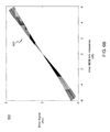
- FIG. 2 is a graph of an example of field and intensity transfer functions of an ideal MZM structure
- FIG. 3A is a diagram of an example of a sub MZM arm imbalance detection and calibration assembly
- FIG. 3B is a diagram of an example of a sub MZM arm imbalance detection and calibration flowchart
- FIG. 4A is a graph of an example of a first order harmonic of phase error signals monitored on the In-phase (I) arm for different Quadrature (Q) sub MZM arm imbalances;
- FIG. 4B is a graph of an example of a second order harmonic of phase error signals monitored on the I arm for different Q sub MZM arm imbalances
- FIG. 5 is a graph of an example of the absolute values of phase error signals monitored on the I arm for different Q sub MZM arm imbalances
- FIG. 6A is a graph of an example of obtained error signals by sweeping different sub MZM arm imbalances.
- FIG. 6B is a graph of another example of obtained error signals by sweeping different sub MZM arm imbalances.
- An optical transmitter may include an MZM.
- the MZM may split light into a first portion for an in-phase arm of the MZM and a second portion for a quadrature arm of the MZM.
- the optical transmitter may apply modulator arm adjustments and dither signals to the two portions.
- the MZM may combine the two portions into an optical output signal.
- the optical transmitter may tap the optical output signal to provide a first portion of the optical output signal to circuits and transmit a second portion to a communications system.
- the optical transmitter using the circuits, may obtain first error signals based on the first dither signal of the first portion of the output signal, and second error signals based on the second dither signal of the first portion of the output signal.
- the optical transmitter may change the modulator arm adjustments based on the error signals.
- the optical transmitter may detect characteristics of the error signals and determine changes to the modulator arm adjustments based on the characteristics.
- a dither signal may include one or more dither tones.
- examples disclosed herein include a method to determine and monitor a potential loss imbalance between the two arms of an MZM located, which may be referred to as a sub-MZM or a child MZM, within an outer MZM structure, which may be referred to as a super or parent MZM.
- the methods described herein are superior with respect to blocking arm by arm of the two inner MZMs, the child MZMs, within the super MZM because the methods do not require any blocking and are therefore potentially exercisable during normal operation.
- examples disclosed herein do not suffer from changes induced by blocking and the implicated absorption of light which alters the energy state of the system.
- VOAs variable optical attenuators
- FIG. 1A is a schematic of an example MZM interferometer used as an optical modulator.
- FIG. 1B is a schematic of an example of a nested MZM structure used to modulate complex signals onto an optical carrier.
- the incoming light which may be generated by a laser, may be split into two arms in each of which a phase shift may be applied.
- the incoming light may include optical field inputs 110 , 160 which may be represented by E in .
- the induced phases may be denoted as ⁇ p and ⁇ n , respectively.
- the output light may include optical field outputs 120 , 170 which may be represented by E out .
- phase shift elements there may be two phase shift elements per arm one of which is used to modulate a radio frequency (RF) signal and the other one is used to apply a direct current (DC) bias.
- RF radio frequency
- DC direct current
- FIGS. 1A and 1B For the sake of simplicity but will be readily understood by those of ordinary skill in the art.
- VOA variable optical attenuators
- a p and A n respectively.
- the optical field input E in 110 at the MZM interferometer may be split into two arms (p and n) each of which may be applied with a phase shift cp. After the phase shift is applied, the two versions of the field may be combined to form the optical field output E out 120 of the MZM interferometer.
- the optical field input E in 160 may be split into In-phase (I) and Quadrature (Q) arms, which each may then be split into two arms (p and n). These four paths may then be combined to form the optical field output E out 170 of the MZM interferometer.
- E out E in 1 2 ⁇ [ e j ⁇ ⁇ ⁇ p - e j ⁇ ⁇ ⁇ n ] Equation ⁇ ⁇ ( 1 )
- Equation (1) may be further rewritten as follows:
- E out E in j ⁇ ⁇ e j ⁇ ⁇ p + ⁇ n 2 ⁇ sin ⁇ ⁇ p - ⁇ n 2 Equation ⁇ ⁇ ( 2 )
- E out E in 1 2 ⁇ [ A p ⁇ e j ⁇ ⁇ ⁇ p - A n ⁇ e j ⁇ ⁇ ⁇ n ] Equation ⁇ ⁇ ( 3 )
- Equation (3) Equation (3) becomes the following:
- E out E in je j ⁇ ⁇ p + ⁇ n 2 ⁇ sin ⁇ ⁇ p - ⁇ n 2 + ⁇ ⁇ ⁇ A 2 ⁇ e j ⁇ ⁇ ⁇ p ⁇ e j ⁇ ⁇ p + ⁇ n 2 Equation ⁇ ⁇ ( 5 )
- E out E in j ⁇ ⁇ sin ⁇ ⁇ ⁇ + ⁇ ⁇ ⁇ A 2 ⁇ e j ⁇ ⁇ ⁇ Equation ⁇ ⁇ ( 6 )
- an MZM arm imbalance may create an optical field with constant amplitude or carrier with a 90 degree or ⁇ /2 phase with respect to the signal.
- this residual carrier may be compensated using a phase bias set in the other quadrature.
- the overall carrier or unmodulated optical field
- the following equation shows the transfer function for a super MZM structure:
- E out E in [ j ⁇ ⁇ sin ⁇ ⁇ ⁇ I + ⁇ ⁇ ⁇ A I 2 ⁇ e j ⁇ ⁇ I ] + e - j ⁇ ⁇ ⁇ IQ ⁇ [ j ⁇ ⁇ sin ⁇ ⁇ ⁇ Q + ⁇ ⁇ ⁇ A Q 2 ⁇ e j ⁇ ⁇ ⁇ Q ] Equation ⁇ ⁇ ( 7 )
- E out E in [ j ⁇ ⁇ sin ⁇ ⁇ ⁇ I + sin ⁇ ⁇ ⁇ Q ] + ⁇ ⁇ ⁇ A I 2 ⁇ e j ⁇ ⁇ ⁇ I + j ⁇ ⁇ ⁇ ⁇ A Q 2 ⁇ e j ⁇ ⁇ ⁇ Q Equation ⁇ ⁇ ( 8 )
- phase control loop may adjust the phase bias ⁇ of I and Q MZMs until the terms
- FIG. 2 is a graph of an example of field and intensity transfer functions of an ideal MZM structure.
- Graph 200 shows the transfer function of an ideal, arm balanced MZM modulator, such as that in the MZM in FIG. 1A , with respect to the optical field 210 and the optical power or intensity 220 , which may be represented by EE*.
- FIG. 2 shows an example of an MZM transfer function under push-pull operation.
- the MZM may be operated at a point shifted from a point 240 , which may be referred to as a Null Point, and hence a signal may experience more non-linear distortion.
- the optical power or intensity transfer function may include a quadrature point 230 as the operating point of the super MZM structure.
- a goal may be to adjust the 4 arms of a nested MZM structure so that they are well power balanced as part of a calibration process.
- Another goal may be to track degradation while the modulator is deployed in the field. Assuming a laser light source at the input, blocking all modulator arms one by one and measuring the optical power at the output may only serve as an initial set point for power balance but cannot be done in the field without bringing data traffic down. Furthermore, blocking the light in individual arms may heat up the modulator locally which may change the overall bias conditions through thermal crosstalk. Therefore, an accurate and efficient method would improve calibrating and tracking MZM arm imbalances without the need to block individual arms.
- the methods described herein may be performed on a variety of devices.
- the devices described herein are for illustrative purposes and the methods may be performed on other devices known to one of ordinary skill in the art without loss of functionality.
- the methods described herein may be performed on an optical modulator.
- the optical modulator may be an MZM.
- the methods described herein may be performed in the digital domain or the analog domain, or a combination of the digital and analog domains.
- FIG. 3A is a diagram of an example of a sub MZM arm imbalance detection and calibration assembly.
- Diagram 300 shows a potential setup that can be used to detect sub MZM arm imbalance and may be an optical transmitter. Signals, which may be referred to as dither signals, may be added to the transmitted signal and detected locally, such as at the transmitter.
- a dither signal may include one or more dither tones.
- a light source 310 which may be a laser source, such as a laser diode, may generate an optical field MZM input for an optical modulator or an MZM structure 320 , which may be similar to the MZM structure shown in FIG. 1A , the nested MZM structure shown in FIG. 1B or another MZM structure.
- a signal for transmission which may be a high speed RF signal, may be generated by a signal generator 337 .
- the signal for transmission may include a payload or data signal.
- Dither tones 333 , 334 may then be added to the signal at junctions 335 , 336 and fed into digital to analog converters (DACs) 331 , 332 .
- DACs digital to analog converters
- the DACs may then produce analog signals which are used by the MZM structure 320 .
- the dither tones may be added at other points and not only at the ASIC.
- the dither tones may be added at the output of the DACs.
- the dither tones may be added to the DC voltage applied to the DC phase adjustors of the MZM, as described herein below.
- the dither tones may be added to the DC phase adjustors in the analog domain.
- the dither tones may also be added by electrical drive signal source sources, in an example.
- the MZM may send an optical field output, which may be denoted as E(t) to optical splitter 340 .
- Optical splitter 340 may split the optical signal into optical output 345 and a signal used to detect the dither signals and determine the arm imbalance. In an example, 90% of the signal from optical splitter 340 may be optical output 345 and 10% may be used for detection, however other percentages may be used without loss of functionality.
- the dither signals may be detected using a single low-speed photo detector 347 .
- the arm imbalance may then be determined based on the dither signals, as explained more fully herein.
- photo detector 347 may include a photo diode and a trans-impedance amplifier.
- Photo detector 347 may generate an electrical signal as output, which may be represented by i(t) and fed into a low pass filter 350 .
- the output of low pass filter 350 may be input into an analog to digital converter (ADC) 355 and be subject to and digital signal processing (DSP).
- ADC analog to digital converter
- DSP digital signal processing
- the output of ADC 355 may be fed into splitter 360 , which may split the signal into four signals and output each of the four signals into one of four different respective correlators.
- the correlators may be circuits. Each correlator may include multipliers and accumulators for real and imaginary parts of the signal. For example, a first correlator may include complex multiplier 362 and accumulator 372 , a second correlator may include complex multiplier 364 and accumulator 374 , a third correlator may include complex multiplier 366 and accumulator 376 and a fourth correlator may include complex multiplier 368 and accumulator 378 . Correlators may provide outputs for use by tone processing 380 , which may detect and process the dither tones 333 , 334 used in MZM structure 320 . In example, the correlators may also include splitter 360 .
- a dither detection and processing device may perform some or all of the steps performed by, or include some or all of, the following components: the photo detector 347 , the low pass filter 350 , the splitter 360 , complex multipliers 362 , 364 , 366 , 368 , accumulators 372 , 374 , 376 , 378 and tone processing 380 .
- the tone processing 380 may be performed by a variety of devices or components.
- tone processing 380 may be performed by a processor.
- the processor may be an analog processor or a digital processor.
- the processor may be a microprocessor, a microcontroller, a processing unit or a field-programmable gate array (FPGA).
- the tone processing 380 may be performed external to or remote from the optical transmitter.
- tone processing 380 may provide instructions to the attenuators to adjust the attenuation.
- the dither tones may either be added digitally within an ASIC.
- the dither tones may be added as analog electrical tones either to the RF signal or they are added to the DC signals fed to the MZM DC electrodes used to set the MZM phase bias.
- the dither tones may be added to the RF signal using a bias tee or a diplexer, which may include a capacitor and an inductor. Applying a dither signal may be considered to be applying a periodic variation to a constant.
- the dither signals d I 334 and A 333 may be added digitally and fed to DACs 332 , 331 together with the high speed signal 337 .
- the outputs of DACs 332 , 331 may be used to drive a nested MZM structure 320 .
- the processing may include a potential second polarization.
- Individual signals may be carried on the I and Q quadratures, each of which can be a differential signal with p and n physical paths.
- s I,Q,n (t) ⁇ s I,Q,p (t) to ensure push-pull operation of the MZMs.
- the optical output of the modulator may be tapped, detected and digitized, as described herein. Again, the processing could have been performed in the analog domain as well.
- a set of four correlators may be needed to detect frequencies associated with the tones d I and d Q .
- Tone processing as described in more detail herein may produce signals, which may be referred to as error signals, that may be used to control the respective arm loss in the nested MZM structure through, for example, VOAs.
- VOAs are commonly used in integrated optical modulator structures to tolerate a certain distribution of splitting ratios and insertion loss.
- FIG. 3B is a diagram of an example of a sub MZM arm imbalance detection and calibration flowchart.
- an optical modulator may split an optical field input into portions.
- Light may be considered to be an optical field input.
- the optical modulator may be an MZM.
- the MZM may receive light and then supply a first portion of the light to the in-phase arm of the MZM and a second portion of the light to the quadrature arm of the MZM 381 .
- An electrical drive signal source may apply a first modulator arm adjustment and a first dither signal to the first portion of the light in the in-phase arm and a second modulator arm adjustment and a second dither signal to the second portion of the light in the quadrature arm 382 .
- a dither signal may include one or more dither tones.
- the dither signals may include AM dither tones.
- the first modulator arm adjustment may be a first modulator arm adjustment drive signal and the second modulator arm adjustment may be a second modulator arm adjustment drive signal
- the MZM may then combine the first and second portions of the light from the in-phase arm and the quadrature phase arm, respectively, into an optical output signal 383 .
- a splitter may tap the optical output signal to provide a first portion of the optical output signal to first and second correlators (which may be circuits), and may transmit a second portion of the optical output signal to a communication system 384 .
- a first correlator may obtain one or more first error signals based on the first dither signal of the first portion of the output signal, and one or more second error signals based on the second dither signal of the first portion of the optical output signal 385 .
- the first correlator may be a first circuit and the second correlator may be a second circuit.
- a processor may determine a first change to the first modulator arm adjustment based on the one or more second error signals and a second change to the second modulator arm adjustment based on the one or more first error signals 388 . Further, the processor may provide, to the electrical drive signal source, the first change to first modulator arm adjustment and the second change to second modulator arm adjustment 389 . The electrical drive signal source may then apply these changes in a manner similar to that described above.
- the above components of the optical transmitter may be operatively connected to each other.
- applying the first change and applying the second change may be performed in a control loop.
- the control loop may run on a continuous, iterative basis.
- the processor of the optical transmitter may detect first characteristics of the obtained first error signals and second characteristics of the obtained second error signals. The processor may then determine the first change to the first modulator arm adjustment based on the detected second characteristics and the second change to the second modulator arm adjustment based on the detected first characteristics.
- the first modulator arm adjustment may be a first modulator arm phase adjustment.
- the second modulator arm adjustment may be a second modulator arm phase adjustment.
- the first modulator arm adjustment may be a first modulator arm amplitude adjustment.
- the second modulator arm adjustment may be a second modulator arm amplitude adjustment.
- the characteristics may include at least one of a minimum, a maximum and a null. Further, the characteristics may be determined based on at least one of first order harmonics, second order harmonics and amplitude modulated (AM) dither tones. The characteristics of the first order harmonics, second order harmonics and AM dither tones are described more fully herein below.
- the dither tone of Equation (9) may be applied as dither tone 334 .
- A may be the tone amplitude and ⁇ be the sub MZM phase.
- the described dither and error signals are usually used and observed in current MZM phase controls. Therefore no complexity may be added by the sub MZM balance control scheme up to this point.
- FIG. 4A is a graph of an example of a first order harmonic of phase error signals monitored on the In-phase (I) arm for different Quadrature (Q) sub MZM arm imbalances.
- a graphical interpretation of Equation (10) is shown in FIG. 4A for the detection of error signals on the I quadrature and for different arm imbalances ⁇ A in the Q quadrature.
- an arm imbalance in the Q sub MZM may lead to a vertical shift of the phase error signal in the I sub MZM, as observed by a state of the art phase control.
- a phase control loop may result in a sub MZM phase at which the error signal is zero.
- the amplitude of the second order harmonic 2 ⁇ I,Q may be proportional to the cosine of the same, according to the following equation: x 2 ⁇ I,Q ( ⁇ ) ⁇ cos 2 ⁇ Equation (11)
- FIG. 4B is a graph of an example of a second order harmonic of phase error signals monitored on the I arm for different Q sub MZM arm imbalances.
- FIG. 4B shows a graphic interpretation of Equation (11) for the detection of error signals on the I quadrature for the same different arm imbalances ⁇ A in the Q quadrature ( 460 , 470 , 480 ) as shown in FIG. 4A ( 410 , 420 , 430 ).
- the arm imbalance ⁇ A induced shift of the phase error curve may be much weaker for the second order harmonic than for the first order result. With this difference in shift, an error signal for ⁇ A may be obtained by comparing the locations of first order harmonic zero in FIG. 4A and the second order harmonic maximum in FIG. 4B .
- phase ⁇ may be assessed by slightly varying the sub MZM phase which may be done without significantly impacting the transmitted signal.
- the described method may be a candidate to be used for active in-service sub MZM arm balance monitoring and control.
- an AM tone may be added. This is another variant of the proposed scheme which may provide greater flexibility in choosing a second frequency for both dither and correlator.
- the AM tone may be defined by the following equation:
- Equation (12) in may be the modulation index, A may be the amplitude, ⁇ AM may be the AM frequency, and ⁇ c may be the carrier frequency. Instead of assessing the second order harmonic, one may assess ⁇ AM instead. The rest may be identical to what is described above herein.
- the absolute value of the first order sub MZM phase error signal can be looked at. Essentially this is the same signal shown in FIG. 4A with an additional sign removal by looking at the absolute value.
- FIG. 5 is a graph of an example of the absolute values of phase error signals monitored on the I arm for different Q phase arm sub MZM imbalances.
- FIG. 5 may be considered as an absolute value of error signal detection analog to FIG. 4A .
- graph 500 by comparing the maximum value seen for ⁇ 0 to the maximum value seen for ⁇ >0, the sub MZM arm imbalance in the opposite arm may be quantified. For this method no assessment of the second order harmonic may be required and a single dither may suffice per sub MZM.
- FIG. 6A is a graph of an example of obtaining error signals by sweeping different sub MZM arm imbalances.
- the error signals 610 in graph 600 may be obtained by determining the difference between the ⁇ at which the phase error signal equals 0 in the first order harmonic, per FIG. 4A , and the ⁇ at which the error signal is at its maximum in the second order harmonic, per FIG. 4B .
- FIG. 6B is a graph of another example of obtaining error signals by sweeping different arm sub MZM imbalances.
- the error signals 660 may be obtained by determining the difference between the maxima at ⁇ 0 and at ⁇ >0, per FIG. 5 .
- processors include, by way of example, a general purpose processor, a special purpose processor, a conventional processor, a digital signal processor (DSP), a plurality of microprocessors, one or more microprocessors in association with a DSP core, a controller, a microcontroller, metal-oxide semiconductor field-effect transistors (MOSFETs), ASICs, FPGAs circuits, any other type of integrated circuit (IC), and/or a state machine.
- DSP digital signal processor
- MOSFETs metal-oxide semiconductor field-effect transistors
- ASICs application-programmable gate array
- FPGAs circuits any other type of integrated circuit (IC), and/or a state machine.
- Such processors may be manufactured by configuring a manufacturing process using the results of processed hardware description language (HDL) instructions and other intermediary data including netlists (such instructions capable of being stored on a computer readable media). The results of such processing may be maskworks that are then used in a semiconductor manufacturing process to manufacture a processor that implements aspects of the
- the suitable processors may include circuitry to implement the methods provided herein.
- the circuitry may include receiving circuitry, processing circuitry and transmitting circuitry.
- non-transitory computer-readable storage media include, but are not limited to, a read only memory (ROM), a random access memory (RAM), a register, cache memory, semiconductor memory devices, magnetic media such as internal hard disks and removable disks, magneto-optical media, and optical media such as CD-ROM disks, and digital versatile disks (DVDs).
- ROM read only memory
- RAM random access memory
- register cache memory
- semiconductor memory devices magnetic media such as internal hard disks and removable disks, magneto-optical media, and optical media such as CD-ROM disks, and digital versatile disks (DVDs).
- the devices according to various embodiments described herein may be interspersed among other devices depending on the functionality of the microelectronic device.
- the number and components of the devices may vary depending on the functionality of the microelectronic device.
- the number of correlators may vary from two to dozens.
Landscapes
- Physics & Mathematics (AREA)
- Nonlinear Science (AREA)
- Optics & Photonics (AREA)
- Electromagnetism (AREA)
- General Physics & Mathematics (AREA)
- Engineering & Computer Science (AREA)
- Computer Networks & Wireless Communication (AREA)
- Signal Processing (AREA)
- Optical Modulation, Optical Deflection, Nonlinear Optics, Optical Demodulation, Optical Logic Elements (AREA)
Abstract
Description
may lead to an optical field that is not fully suppressed at ϕ=0 and can therefore be referred to as carrier leakage. State of the art optical modulators are phase controlled. In the case of non-zero carrier leakage, a phase control loop may adjust the phase bias ϕ of I and Q MZMs until the terms
vanish. However, compensating for arm imbalance in one of the sub MZMs by adjusting the phase bias in the opposite MZM arm, comes at a price of increased MZM non-linearity.
d I,Q(t)=A cos ωI,Q t Equation (9)
The dither tone of Equation (9) may be applied as
x ω
In Equation (10), A may be the tone amplitude and ϕ be the sub MZM phase. The described dither and error signals are usually used and observed in current MZM phase controls. Therefore no complexity may be added by the sub MZM balance control scheme up to this point.
x 2ω
In Equation (12), in may be the modulation index, A may be the amplitude, ωAM may be the AM frequency, and ωc may be the carrier frequency. Instead of assessing the second order harmonic, one may assess ωAM instead. The rest may be identical to what is described above herein.
Claims (22)
Priority Applications (1)
| Application Number | Priority Date | Filing Date | Title |
|---|---|---|---|
| US15/382,203 US10082718B2 (en) | 2016-12-16 | 2016-12-16 | Non-blocking mach-zehnder modulator arm imbalance monitoring and control through tones |
Applications Claiming Priority (1)
| Application Number | Priority Date | Filing Date | Title |
|---|---|---|---|
| US15/382,203 US10082718B2 (en) | 2016-12-16 | 2016-12-16 | Non-blocking mach-zehnder modulator arm imbalance monitoring and control through tones |
Publications (2)
| Publication Number | Publication Date |
|---|---|
| US20180173077A1 US20180173077A1 (en) | 2018-06-21 |
| US10082718B2 true US10082718B2 (en) | 2018-09-25 |
Family
ID=62562413
Family Applications (1)
| Application Number | Title | Priority Date | Filing Date |
|---|---|---|---|
| US15/382,203 Active US10082718B2 (en) | 2016-12-16 | 2016-12-16 | Non-blocking mach-zehnder modulator arm imbalance monitoring and control through tones |
Country Status (1)
| Country | Link |
|---|---|
| US (1) | US10082718B2 (en) |
Cited By (4)
| Publication number | Priority date | Publication date | Assignee | Title |
|---|---|---|---|---|
| US20220021462A1 (en) * | 2020-07-14 | 2022-01-20 | Infinera Corp. | Digital tone-based apparatus and method for measuring the frequency response of coherent optical transmitters |
| US20220239382A1 (en) * | 2021-01-26 | 2022-07-28 | Nokia Solutions And Networks Oy | In-phase to quadrature-phase imbalance in an optical data modulator |
| US20220404678A1 (en) * | 2021-06-16 | 2022-12-22 | Fujitsu Optical Components Limited | Optical transmitter, optical transceiver, and method of controlling bias voltage of electro-optic modulator |
| US20230068004A1 (en) * | 2021-08-25 | 2023-03-02 | Electronics And Telecommunications Research Institute | Silicon photonics-based optical modulator |
Families Citing this family (3)
| Publication number | Priority date | Publication date | Assignee | Title |
|---|---|---|---|---|
| CN109643030B (en) * | 2017-03-17 | 2023-12-15 | 洛克利光子有限公司 | Optical modulators and methods of use |
| US12001115B2 (en) | 2017-03-17 | 2024-06-04 | Rockley Phonics Limited | Optical modulator and method of use |
| US10498454B1 (en) * | 2018-06-29 | 2019-12-03 | Cisco Technology, Inc. | Extinction ratio improvements in silicon photonics |
Citations (1)
| Publication number | Priority date | Publication date | Assignee | Title |
|---|---|---|---|---|
| US9166697B2 (en) * | 2011-04-19 | 2015-10-20 | Nec Corporation | Optical transmitter and method for controlling the same |
-
2016
- 2016-12-16 US US15/382,203 patent/US10082718B2/en active Active
Patent Citations (1)
| Publication number | Priority date | Publication date | Assignee | Title |
|---|---|---|---|---|
| US9166697B2 (en) * | 2011-04-19 | 2015-10-20 | Nec Corporation | Optical transmitter and method for controlling the same |
Cited By (8)
| Publication number | Priority date | Publication date | Assignee | Title |
|---|---|---|---|---|
| US20220021462A1 (en) * | 2020-07-14 | 2022-01-20 | Infinera Corp. | Digital tone-based apparatus and method for measuring the frequency response of coherent optical transmitters |
| US11799558B2 (en) * | 2020-07-14 | 2023-10-24 | Infinera Corporation | Digital tone-based apparatus and method for measuring the frequency response of coherent optical transmitters |
| US20220239382A1 (en) * | 2021-01-26 | 2022-07-28 | Nokia Solutions And Networks Oy | In-phase to quadrature-phase imbalance in an optical data modulator |
| US11588559B2 (en) * | 2021-01-26 | 2023-02-21 | Nokia Solutions And Networks Oy | In-phase to quadrature-phase imbalance in an optical data modulator |
| US20220404678A1 (en) * | 2021-06-16 | 2022-12-22 | Fujitsu Optical Components Limited | Optical transmitter, optical transceiver, and method of controlling bias voltage of electro-optic modulator |
| US11852948B2 (en) * | 2021-06-16 | 2023-12-26 | Fujitsu Optical Components Limited | Optical transmitter, optical transceiver, and method of controlling bias voltage of electro-optic modulator |
| US20230068004A1 (en) * | 2021-08-25 | 2023-03-02 | Electronics And Telecommunications Research Institute | Silicon photonics-based optical modulator |
| US11899334B2 (en) * | 2021-08-25 | 2024-02-13 | Electronics And Telecommunications Research Institute | Silicon photonics-based optical modulator |
Also Published As
| Publication number | Publication date |
|---|---|
| US20180173077A1 (en) | 2018-06-21 |
Similar Documents
| Publication | Publication Date | Title |
|---|---|---|
| US10082718B2 (en) | Non-blocking mach-zehnder modulator arm imbalance monitoring and control through tones | |
| CN110031832B (en) | Microwave photon Doppler frequency shift measurement system and adjusting method thereof | |
| US9960854B2 (en) | Method and system for the monolithic integration of circuits for monitoring and control of RF signals | |
| US7266306B1 (en) | Method for optical carrier suppression and quadrature control | |
| CN101800598B (en) | New Balance Detection Bias Control Method for MZ External Modulator | |
| Li et al. | Arbitrary bias point control technique for optical IQ modulator based on dither-correlation detection | |
| JP2008116448A (en) | System and method for alleviating polarization mode dispersion | |
| JP6540952B2 (en) | Method of generating optical two-tone signal and control method of DP-MZM type light modulator | |
| CN108306689A (en) | Double parallel Mach-Zehnder modulators based on three pilot tones(DPMZM)Arbitrary point autobias control method | |
| CN107741525B (en) | Photodetector frequency response measurement method and device | |
| JP2019004296A (en) | Optical transmitter and skew compensation method | |
| WO2018040383A1 (en) | Debugging method and device for operating point voltage of parallel mzi electro-optical modulator | |
| WO2022022157A1 (en) | Automatic bias control apparatus and method for direct-modulation and direct-detection optical modulator | |
| CN113541787A (en) | A functionally flexible photonics-assisted frequency measurement method and device | |
| JP2016099358A (en) | Phase adjustor, phase adjustment method, and test system | |
| JP2023178277A (en) | Optical multiple-input-multiple-output (mimo) receiver using stokes vector measurements | |
| JP5622154B2 (en) | Evaluation method of optical modulator with multiple Mach-Zehnder interferometers | |
| Zheng et al. | Integrated Microwave Photonics Multi‐Parameter Measurement System | |
| JP7157552B2 (en) | How to use electro-optical sensors and Mach-Zehnder modulators | |
| Hutchinson et al. | Mitigation of photodiode induced even-order distortion in photonic links with predistortion modulation | |
| Sutili et al. | Optical modulator half-wave voltage measurement using opposite-phase sine waves | |
| US9438352B2 (en) | QPSK signal conjugate relationship identification method and apparatus, and dispersion compensation method and system | |
| Torrijos-Morán et al. | Linearization of a dual-parallel Mach-Zehnder modulator using optical carrier band processing | |
| CN107204803A (en) | A kind of polarization mode dispersion monitoring method and system based on PPM Transmission systems | |
| CN113225126B (en) | Test system and measurement method of phase modulator |
Legal Events
| Date | Code | Title | Description |
|---|---|---|---|
| AS | Assignment |
Owner name: INFINERA CORPORATION, CALIFORNIA Free format text: ASSIGNMENT OF ASSIGNORS INTEREST;ASSIGNOR:SCHMOGROW, RENE MARCEL;REEL/FRAME:040642/0300 Effective date: 20161216 |
|
| STCF | Information on status: patent grant |
Free format text: PATENTED CASE |
|
| MAFP | Maintenance fee payment |
Free format text: PAYMENT OF MAINTENANCE FEE, 4TH YEAR, LARGE ENTITY (ORIGINAL EVENT CODE: M1551); ENTITY STATUS OF PATENT OWNER: LARGE ENTITY Year of fee payment: 4 |
|
| MAFP | Maintenance fee payment |
Free format text: PAYMENT OF MAINTENANCE FEE, 8TH YEAR, LARGE ENTITY (ORIGINAL EVENT CODE: M1552); ENTITY STATUS OF PATENT OWNER: LARGE ENTITY Year of fee payment: 8 |