US10081871B2 - Metal oxide film structure - Google Patents
Metal oxide film structure Download PDFInfo
- Publication number
- US10081871B2 US10081871B2 US14/903,239 US201414903239A US10081871B2 US 10081871 B2 US10081871 B2 US 10081871B2 US 201414903239 A US201414903239 A US 201414903239A US 10081871 B2 US10081871 B2 US 10081871B2
- Authority
- US
- United States
- Prior art keywords
- metal oxide
- layer structure
- oxide layer
- particles
- substrate
- Prior art date
- Legal status (The legal status is an assumption and is not a legal conclusion. Google has not performed a legal analysis and makes no representation as to the accuracy of the status listed.)
- Active, expires
Links
Images


Classifications
-
- C—CHEMISTRY; METALLURGY
- C23—COATING METALLIC MATERIAL; COATING MATERIAL WITH METALLIC MATERIAL; CHEMICAL SURFACE TREATMENT; DIFFUSION TREATMENT OF METALLIC MATERIAL; COATING BY VACUUM EVAPORATION, BY SPUTTERING, BY ION IMPLANTATION OR BY CHEMICAL VAPOUR DEPOSITION, IN GENERAL; INHIBITING CORROSION OF METALLIC MATERIAL OR INCRUSTATION IN GENERAL
- C23C—COATING METALLIC MATERIAL; COATING MATERIAL WITH METALLIC MATERIAL; SURFACE TREATMENT OF METALLIC MATERIAL BY DIFFUSION INTO THE SURFACE, BY CHEMICAL CONVERSION OR SUBSTITUTION; COATING BY VACUUM EVAPORATION, BY SPUTTERING, BY ION IMPLANTATION OR BY CHEMICAL VAPOUR DEPOSITION, IN GENERAL
- C23C24/00—Coating starting from inorganic powder
- C23C24/02—Coating starting from inorganic powder by application of pressure only
- C23C24/04—Impact or kinetic deposition of particles
-
- C—CHEMISTRY; METALLURGY
- C23—COATING METALLIC MATERIAL; COATING MATERIAL WITH METALLIC MATERIAL; CHEMICAL SURFACE TREATMENT; DIFFUSION TREATMENT OF METALLIC MATERIAL; COATING BY VACUUM EVAPORATION, BY SPUTTERING, BY ION IMPLANTATION OR BY CHEMICAL VAPOUR DEPOSITION, IN GENERAL; INHIBITING CORROSION OF METALLIC MATERIAL OR INCRUSTATION IN GENERAL
- C23C—COATING METALLIC MATERIAL; COATING MATERIAL WITH METALLIC MATERIAL; SURFACE TREATMENT OF METALLIC MATERIAL BY DIFFUSION INTO THE SURFACE, BY CHEMICAL CONVERSION OR SUBSTITUTION; COATING BY VACUUM EVAPORATION, BY SPUTTERING, BY ION IMPLANTATION OR BY CHEMICAL VAPOUR DEPOSITION, IN GENERAL
- C23C24/00—Coating starting from inorganic powder
- C23C24/02—Coating starting from inorganic powder by application of pressure only
-
- C—CHEMISTRY; METALLURGY
- C04—CEMENTS; CONCRETE; ARTIFICIAL STONE; CERAMICS; REFRACTORIES
- C04B—LIME, MAGNESIA; SLAG; CEMENTS; COMPOSITIONS THEREOF, e.g. MORTARS, CONCRETE OR LIKE BUILDING MATERIALS; ARTIFICIAL STONE; CERAMICS; REFRACTORIES; TREATMENT OF NATURAL STONE
- C04B41/00—After-treatment of mortars, concrete, artificial stone or ceramics; Treatment of natural stone
- C04B41/45—Coating or impregnating, e.g. injection in masonry, partial coating of green or fired ceramics, organic coating compositions for adhering together two concrete elements
- C04B41/4505—Coating or impregnating, e.g. injection in masonry, partial coating of green or fired ceramics, organic coating compositions for adhering together two concrete elements characterised by the method of application
- C04B41/4515—Coating or impregnating, e.g. injection in masonry, partial coating of green or fired ceramics, organic coating compositions for adhering together two concrete elements characterised by the method of application application under vacuum or reduced pressure
-
- C—CHEMISTRY; METALLURGY
- C04—CEMENTS; CONCRETE; ARTIFICIAL STONE; CERAMICS; REFRACTORIES
- C04B—LIME, MAGNESIA; SLAG; CEMENTS; COMPOSITIONS THEREOF, e.g. MORTARS, CONCRETE OR LIKE BUILDING MATERIALS; ARTIFICIAL STONE; CERAMICS; REFRACTORIES; TREATMENT OF NATURAL STONE
- C04B41/00—After-treatment of mortars, concrete, artificial stone or ceramics; Treatment of natural stone
- C04B41/45—Coating or impregnating, e.g. injection in masonry, partial coating of green or fired ceramics, organic coating compositions for adhering together two concrete elements
- C04B41/4505—Coating or impregnating, e.g. injection in masonry, partial coating of green or fired ceramics, organic coating compositions for adhering together two concrete elements characterised by the method of application
- C04B41/4545—Coating or impregnating, e.g. injection in masonry, partial coating of green or fired ceramics, organic coating compositions for adhering together two concrete elements characterised by the method of application applied as a powdery material
Definitions
- the present invention relates, in general, to a metal oxide layer structure formed on the surface of a substrate, and more particularly, to a metal oxide layer structure in which the atomic numbers of the element metal and the element oxygen in the metal oxide layer are in a non-stoichiometric ratio, so that the metal oxide layer has a high density corresponding to 90-100% of the metal oxide before coating and is free of cracks and pores.
- Metal oxides are compounds composed of metal atoms bonded to oxygen atoms and are used as coating materials in the industry. As shown in Table 1 below, metal oxides have characteristic densities.
- Metal oxides include yttrium oxide (Y 2 O 3 ), aluminum oxide (Al 2 O 3 ), magnesium oxide (MgO), zinc oxide (ZnO), tin oxide (SnO), iron oxide (FeO), titanium oxide (TiO 2 ), zirconium oxide (ZrO 2 ), chromium oxide (Cr 2 O 3 ), hafnium oxide (HfO), beryllium oxide (BeO) and the like. As shown in Table 1 below, such metal oxides are stoichiometric compounds in which the atomic number of each of elements forming the metal oxides is a simple integer.
- the density of the metal oxide layer compared to the metal oxide before coating is important. In other words, as the density of the metal oxide layer is closer to the density of the metal oxide before coating, the metal oxide layer exhibits better physical or chemical properties. In addition, the more density of the metal oxide layer increases, the more surface hardness thereof also increases. Table 1 below summarizes the atomic number of each element in each metal oxide, the atomic percent of each element in each metal oxide, and the density of each metal oxide.
- LEDs light-emitting diodes
- processes including deposition, etching, ashing, diffusion, cleaning and the like are performed.
- impurities (particles) generated during the processes adhere to the surfaces of substrates in process chambers, and then are detached during the processes to thereby contaminate wafers.
- substrate surfaces are required to have anti-particle adhesion so as to minimize the adhesion of such particles to the substrate surfaces.
- references 1 and 2 below disclose a mechanism in which an amorphous coating layer is formed on a substrate using pulsed laser deposition (PLD; a kind of physical vapor deposition (PVD)) by irradiating a laser onto a target composed of a coating material (YSZ; yttria-stabilized zirconia) to vapor-deposit the coating material onto the substrate in a vacuum state, and the amorphous coating layer is crystallized by heating it to a temperature ranging from several tens to hundreds of degrees centigrade (° C.).
- PLD pulsed laser deposition
- PVD physical vapor deposition
- Another object of the present invention is to provide a layer structure which is fabricated by forming an yttrium oxide layer on the substrate surface using yttrium oxide (Y 2 O 3 ) powder having excellent anti-corrosive and anti-plasma properties against fluorine-based gas, chlorine-based gas and the like, thereby greatly improving the anti-particle adhesion property of the substrate surface.
- Y 2 O 3 yttrium oxide
- the present invention provides a metal oxide layer structure formed on the surface of a substrate, the metal oxide layer structure being formed of a metal oxide represented by X a Y b (X: a metal element, Y: the element oxygen, a: the atomic number of the metal element, and b: the atomic number of the element oxygen), wherein the atomic percent of the metal element in the metal oxide layer structure is greater than ⁇ a/(a+b) ⁇ 100(%).
- the layer structure is composed of nano-crystalline particles and nano-amorphous particles. The particles forming the layer structure do not undergo heat-induced growth and heat-induced conversion to crystalline particles and the layer structure is free of cracks and pores.
- the above metal oxide layer structure may be fabricated using a solid powder spray coating method in which a carrier gas consisting of a mixture of a suction gas, sucked in a transport pipe by a negative pressure formed in a coating chamber containing a spray nozzle provided at the end of the transport pipe, and a feed gas fed to the transport pipe through a gas feeding unit, transports solid powder introduced into the transport pipe and is sprayed through the spray nozzle, so that the solid powder is spray-coated on a substrate in the coating chamber which is in a vacuum state.
- a carrier gas consisting of a mixture of a suction gas, sucked in a transport pipe by a negative pressure formed in a coating chamber containing a spray nozzle provided at the end of the transport pipe, and a feed gas fed to the transport pipe through a gas feeding unit, transports solid powder introduced into the transport pipe and is sprayed through the spray nozzle, so that the solid powder is spray-coated on a substrate in the coating chamber which is in a vacuum state.
- the metal oxide layer structure according to the present invention can be widely used in the semiconductor and electronic fields:
- the metal oxide layer structure dramatically reduces the amount of particles adhering to the surface of a substrate during processes for the fabrication and treatment of semiconductor devices and the like.
- the metal oxide layer structure makes it possible to continuously and stably perform processes for the fabrication and treatment of semiconductor devices and the like, thereby increasing process yield and productivity.
- the metal oxide layer structure reduces product failure rate after processes for the fabrication and treatment of semiconductor devices and the like.
- the metal oxide layer structure can extend the ex-situ cleaning cycle of consumable substrates and replacement parts.
- the present invention makes it possible to form an yttria layer structure on substrates made of various materials (e.g., ceramic, metal, nonmetal, semimetal and polymer materials, etc.), and thus can be used in processes for the fabrication and treatment of various products.
- various materials e.g., ceramic, metal, nonmetal, semimetal and polymer materials, etc.
- FIG. 1 is a photograph showing the cross-section (spectrum 1) of an yttria (Y 2 O 3 ) layer structure.
- FIG. 2 shows the results of energy dispersive x-ray spectroscopy (EDS) of the cross-section (spectrum 1) of an yttria layer structure.
- EDS energy dispersive x-ray spectroscopy
- FIG. 4 shows the results of energy dispersive x-ray spectroscopy (EDS) of the cross-section (spectrum 7) of an yttria layer structure.
- EDS energy dispersive x-ray spectroscopy
- FIG. 6 is a 5-nm scale TEM image of an yttria layer structure.
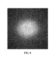
- FIG. 8 is an electron diffraction pattern image of the yttria layer structure shown in FIG. 7 .
- FIG. 10 is a graph showing a comparison of the number of particles on wafers as a function of process time between before and after formation of an yttria layer structure on the wafer surface.
- FIG. 12 is a schematic view of a solid powder-coating apparatus for fabricating a metal oxide layer structure according to the present invention.
- the substrate on which the metal oxide layer structure according to the present invention may be formed may be made of any material selected from among ceramic, metal, nonmetal, semimetal and polymer materials.
- the present inventors have coated yttria (yttrium oxide), a kind of metal oxide, on the surface of a substrate, thereby forming an yttria layer structure in which the atomic number of the element yttrium and the atomic number of the element oxygen are in a non-stoichiometric ratio.
- the atomic percent of the element yttrium in the layer structure is greater than the atomic percent of yttrium present in stoichiometric yttrium oxide.
- the metal oxide is represented by X a Y b (X: the element metal, Y: the element oxygen, a: the atomic number of the element metal, and b: the atomic number of the element oxygen), the atomic percent of the element metal in the metal oxide layer structure is greater than ⁇ a/(a+b) ⁇ 100(%).
- FIGS. 1 and 3 show the cross-sections (spectrum 1 and spectrum 7) of the yttria layer structure.
- EDS energy dispersive x-ray spectroscopy
- Y element yttrium
- O element oxygen
- FIGS. 2 and 4 analysis of the atomic percent of each element of yttria in the layer structure indicated characteristics as follows.
- the density of the layer structure formed of the metal oxide yttria was 4.88-4.93 g/cm 3 . This density is high density corresponding to 97.4-98.4% of the yttrium oxide density (5.010 g/cm 3 ) shown in Table 1 above.
- the metal oxide layer structure according to the present invention is characterized in that it is composed of nano-crystalline particles and nano-amorphous particle and the particles forming the layer structure do not undergo heat-induced growth and heat-induced conversion to crystalline particles, and the layer structure is free of cracks and pores.
- the amorphous particles of the yttria layer structure can be grown by heat treatment so as to be converted to crystalline particles, and thus the yttria layer structure can be converted to nanostructures having a polycrystalline electron diffraction pattern.
- FIGS. 4 to 6 a crack-free state can be seen in FIGS. 4 to 6 .
- the amount of particles adhering to the substrate surface and wafers during the processes is significantly reduced as shown in FIGS. 9 and 10 , indicating that the substrate exhibits anti-particle adhesion.
- substrate B before formation
- substrate A after formation
- the metal oxide layer structure according to the present invention is composed of nano-crystalline particles and nano-amorphous particles.
- YSZ yttria-stabilized zirconia particles are deposited on a substrate by pulsed laser deposition (PLD; a kind of physical vapor deposition (PVD)) to form a coating layer made of amorphous particles, and then the coating layer is heated to a temperature ranging from several tens to hundreds of degrees centigrade (° C.) such that the amorphous particles are grown and partially converted to crystalline particles, and the coating layer is completely converted into a crystalline layer by additional heat treatment.
- PLD pulsed laser deposition
- PVD physical vapor deposition
- the metal oxide layer composed of nano-crystalline particles and nano-amorphous particles is formed by a one-step coating process.
- the present invention differs from the prior art technology that requires additional heat treatment of the coating layer to grow the amorphous particles and to convert the amorphous particles into crystalline particles.
- the anti-particle adhesion property of the metal oxide layer structure according to the present invention is also very excellent.
- the surface of the structure differs from the surface layer formed by the thermal spray coating and PLD processes according to the prior art technology, and the structural characteristic of the layer structure according to the present invention differs from that of the prior art technology in that it has the electron diffraction pattern of the amorphous particle layer as shown in FIG. 8 , which cannot be obtained by the prior art technology.
- FIG. 11 is a graph showing a comparison of the number of particles on wafers as a function of the cumulative number of wafers between the case in which an yttria layer structure was formed on the substrate surface by thermal spray coating and the case in which an yttria layer structure was formed on the substrate surface according to the present invention.
- the cumulative number of wafers in the process chamber increases to 100, particles adhering to the substrate are detached and the number of the particles increases cumulatively to 5,000 or more, whereas in the latter case, even when the cumulative number of wafers in the process chamber increases to 100, the number of particles adhering to the substrate is stably maintained at a level of 50 or less.
- the yttria layer structure according to the present invention when the characteristics of the yttria layer structure according to the present invention are exhibited, the number of particles that adhere to the substrate surface and wafers during processes is significantly reduced compared to when the thermal spray coating technique with heating is applied, indicating that the yttria layer structure exhibits stable anti-particle adhesion.
- the application of the present invention is greatly effective.
- the metal oxide layer structure according to the present invention can be fabricated using a solid powder spray coating method in which a carrier gas consisting of a mixture of a suction gas, sucked in a transport pipe by a negative pressure formed in a coating chamber containing a spray nozzle provided at the end of the transport pipe, and a feed gas fed to the transport pipe through a gas feeding unit, transports solid powder introduced into the transport pipe and is sprayed through the spray nozzle, so that the solid powder is spray-coated on a substrate provided in the coating chamber which is in a vacuum state.
- a carrier gas consisting of a mixture of a suction gas, sucked in a transport pipe by a negative pressure formed in a coating chamber containing a spray nozzle provided at the end of the transport pipe, and a feed gas fed to the transport pipe through a gas feeding unit, transports solid powder introduced into the transport pipe and is sprayed through the spray nozzle, so that the solid powder is spray-coated on a substrate provided in the coating chamber which is in
- the above-described solid powder spray coating method can be performed by a solid powder coating apparatus as shown in FIG. 12 , the solid powder coating apparatus comprising: a transport pipe 10 providing a transport channel for solid powder 4 ; a gas feed pipe 15 serving as flow channel for a feed gas that is fed from a gas feeding unit 20 ; a spray nozzle 30 connected to the end of the transport pipe 10 or the gas feed pipe 20 ; a coating chamber 40 containing the spray nozzle 30 ; a solid powder feeding unit (not shown) configured to feed the solid powder 4 , supplied from an environment in which atmospheric pressure is maintained, to the transport pipe 10 ; and a pressure control unit 50 configured to control the internal pressure of the coating chamber 40 , the apparatus being configured such that a gas under atmospheric pressure is sucked in the transport pipe 10 by a negative pressure formed in the coating chamber 40 by operation of the pressure control unit 50 , and a suction gas 1 together with a feed gas 2 serves as a carrier gas 3 for transporting the solid powder 4 .
- the metal oxide layer structure formed on the substrate surface according to the present invention has an increased density and hardness, and thus can minimize the amount of particles adhering to the substrate surface during processes (e.g., semiconductor fabrication processes, display device fabrication processes, etc.). Accordingly, it can industrially substitute for conventional metal oxide coating layers that have required anti-particle adhesion but did not have anti-particle adhesion.
Landscapes
- Chemical & Material Sciences (AREA)
- Engineering & Computer Science (AREA)
- Organic Chemistry (AREA)
- Materials Engineering (AREA)
- Ceramic Engineering (AREA)
- Mechanical Engineering (AREA)
- Metallurgy (AREA)
- Chemical Kinetics & Catalysis (AREA)
- Structural Engineering (AREA)
- Other Surface Treatments For Metallic Materials (AREA)
- Paints Or Removers (AREA)
- Drying Of Semiconductors (AREA)
- Oxygen, Ozone, And Oxides In General (AREA)
Abstract
Description
| TABLE 1 | ||||||||
| Metal | Ele- | Atomic | Atomic | Ele- | Atomic | Atomic | Density | |
| oxide | ment | number | percent | ment | number | percent | (g/cm3) | |
| Al2O3 | Al | 2 | 40.00 | |
3 | 60.00 | 4.100 | |
| Ti2O3 | Ti | 1 | 33.33 | O | 2 | 66.67 | 4.230 | |
| SnO | |
1 | 50.00 | |
1 | 50.00 | 6.450 | |
| SnO2 | |
1 | 33.33 | O | 2 | 66.67 | 6.950 | |
| ZrO2 | Zr | 1 | 33.33 | |
2 | 66.67 | 5.680 | |
| Y2O3 | Y | 2 | 40.00 | |
3 | 60.00 | 5.010 | |
| CrO3 | |
1 | 25.00 | |
3 | 75.00 | 2.700 | |
| Cr2O3 | |
2 | 40.00 | |
3 | 60.00 | 5.220 | |
| HfO2 | |
1 | 33.33 | |
2 | 66.67 | 9.680 | |
| BeO | Be | 1 | 50.00 | |
1 | 50.00 | 3.010 | |
| | Mg | 1 | 50.00 | |
1 | 50.00 | 3.580 | |
| | Fe | 1 | 50.00 | |
1 | 50.00 | 5.745 | |
| Fe2O3 | Fe | 2 | 40.00 | |
3 | 60.00 | 5.242 | |
| ZnO | Zn | 1 | 50.00 | |
1 | 50.00 | 5.606 | |
| BaO | Ba | 1 | 50.00 | |
1 | 50.00 | 5.720 | |
- S. Heiroth et al, Optical and mechanical properties of amorphous and crystalline yttria-stabilized zirconia thin layers prepared by pulsed laser deposition
 , Acta Materialia. 2011, Vol. 59, pp. 2330-2340.
- S. Heiroth et al, Crystallization and grain growth characteristics of yttria-stabilized zirconia thin layers grown by pulsed laser deposition, Solid State Ionics. 2011, Vol. 191, pp. 12-23.

| TABLE 2 | ||
| Metal oxide layer structure | ||
| State | Metal oxide | Atomic percent | Atomic percent |
| Element | Atomic percent | (spectrum 1) | (spectrum 7) |
| O (oxygen) | 60.00 | 21.39 | 45.38 |
| Y (yttrium) | 40.00 | 78.61 | 54.62 |
Claims (5)
Applications Claiming Priority (5)
| Application Number | Priority Date | Filing Date | Title |
|---|---|---|---|
| KR10-2013-0082217 | 2013-07-12 | ||
| KR1020130082217A KR101350294B1 (en) | 2013-07-12 | 2013-07-12 | Uncracked metal oxide layer structure |
| KR10-2013-0133053 | 2013-11-04 | ||
| KR1020130133053A KR101500517B1 (en) | 2013-06-27 | 2013-11-04 | Yttria structure |
| PCT/KR2014/006276 WO2015005735A1 (en) | 2013-07-12 | 2014-07-11 | Metal oxide film structure |
Publications (2)
| Publication Number | Publication Date |
|---|---|
| US20160160358A1 US20160160358A1 (en) | 2016-06-09 |
| US10081871B2 true US10081871B2 (en) | 2018-09-25 |
Family
ID=50145262
Family Applications (1)
| Application Number | Title | Priority Date | Filing Date |
|---|---|---|---|
| US14/903,239 Active 2035-03-08 US10081871B2 (en) | 2013-07-12 | 2014-07-11 | Metal oxide film structure |
Country Status (4)
| Country | Link |
|---|---|
| US (1) | US10081871B2 (en) |
| JP (1) | JP6194112B2 (en) |
| KR (1) | KR101350294B1 (en) |
| CN (1) | CN105392922B (en) |
Families Citing this family (1)
| Publication number | Priority date | Publication date | Assignee | Title |
|---|---|---|---|---|
| KR102082602B1 (en) * | 2018-03-08 | 2020-04-23 | 토토 가부시키가이샤 | Composite structure and display manufacturing apparatus and semiconductor manufacturing device having composite structure |
Citations (9)
| Publication number | Priority date | Publication date | Assignee | Title |
|---|---|---|---|---|
| KR20020063575A (en) | 2000-09-15 | 2002-08-03 | 루센트 테크놀러지스 인크 | Isotropic negative thermal expansion ceramics and process for making |
| RU2211087C1 (en) * | 2002-06-27 | 2003-08-27 | Институт катализа им. Г.К. Борескова СО РАН | Nitrogen monoxide production catalyst and method |
| RU2212934C1 (en) * | 2002-06-27 | 2003-09-27 | Институт катализа им. Г.К. Борескова СО РАН | Catalyst for preparing nitrous oxide and method |
| KR20040034923A (en) | 2002-10-17 | 2004-04-29 | 옵토켐 (주) | Composition for inhibiting triglyceride and functional food comprising same |
| KR20040088045A (en) | 2002-02-06 | 2004-10-15 | 쌩-고벵 글래스 프랑스 | Non-stoichiometric niox ceramic target |
| US20040265587A1 (en) * | 2001-10-30 | 2004-12-30 | Tsuguo Koyanagi | Tubular titanium oxide particles, method for preparing the same, and use of the same |
| KR20060109851A (en) | 2005-04-18 | 2006-10-23 | 산드빅 인터렉츄얼 프로퍼티 에이비 | Coated Insert |
| US20080168717A1 (en) * | 2004-09-23 | 2008-07-17 | Antionette Can | Coated Abrasive Materials And Method Of Manufacture |
| US20090117390A1 (en) * | 2006-03-27 | 2009-05-07 | Werner Stamm | Matrix and Layer System Comprising Non-Stoichiometric Particles |
Family Cites Families (4)
| Publication number | Priority date | Publication date | Assignee | Title |
|---|---|---|---|---|
| US6759085B2 (en) * | 2002-06-17 | 2004-07-06 | Sulzer Metco (Us) Inc. | Method and apparatus for low pressure cold spraying |
| US20100272982A1 (en) * | 2008-11-04 | 2010-10-28 | Graeme Dickinson | Thermal spray coatings for semiconductor applications |
| US8840800B2 (en) * | 2011-08-31 | 2014-09-23 | Kabushiki Kaisha Toshiba | Magnetic material, method for producing magnetic material, and inductor element |
| CN103132002B (en) * | 2011-12-02 | 2015-04-15 | 中国科学院微电子研究所 | A kind of preparation method of black Y2O3 ceramic coating |
-
2013
- 2013-07-12 KR KR1020130082217A patent/KR101350294B1/en active Active
-
2014
- 2014-07-11 JP JP2016525291A patent/JP6194112B2/en active Active
- 2014-07-11 US US14/903,239 patent/US10081871B2/en active Active
- 2014-07-11 CN CN201480038097.3A patent/CN105392922B/en active Active
Patent Citations (11)
| Publication number | Priority date | Publication date | Assignee | Title |
|---|---|---|---|---|
| KR20020063575A (en) | 2000-09-15 | 2002-08-03 | 루센트 테크놀러지스 인크 | Isotropic negative thermal expansion ceramics and process for making |
| US20040265587A1 (en) * | 2001-10-30 | 2004-12-30 | Tsuguo Koyanagi | Tubular titanium oxide particles, method for preparing the same, and use of the same |
| KR20040088045A (en) | 2002-02-06 | 2004-10-15 | 쌩-고벵 글래스 프랑스 | Non-stoichiometric niox ceramic target |
| RU2211087C1 (en) * | 2002-06-27 | 2003-08-27 | Институт катализа им. Г.К. Борескова СО РАН | Nitrogen monoxide production catalyst and method |
| RU2212934C1 (en) * | 2002-06-27 | 2003-09-27 | Институт катализа им. Г.К. Борескова СО РАН | Catalyst for preparing nitrous oxide and method |
| KR20040034923A (en) | 2002-10-17 | 2004-04-29 | 옵토켐 (주) | Composition for inhibiting triglyceride and functional food comprising same |
| US20080168717A1 (en) * | 2004-09-23 | 2008-07-17 | Antionette Can | Coated Abrasive Materials And Method Of Manufacture |
| KR20060109851A (en) | 2005-04-18 | 2006-10-23 | 산드빅 인터렉츄얼 프로퍼티 에이비 | Coated Insert |
| US20060257691A1 (en) * | 2005-04-18 | 2006-11-16 | Sandvik Intellectual Property Ab | Coated insert |
| US20090117390A1 (en) * | 2006-03-27 | 2009-05-07 | Werner Stamm | Matrix and Layer System Comprising Non-Stoichiometric Particles |
| JP2009531543A (en) | 2006-03-27 | 2009-09-03 | シーメンス アクチエンゲゼルシヤフト | Matrix and layer structure with non-stoichiometric particles |
Non-Patent Citations (2)
| Title |
|---|
| S. Heiroth et al., "Crystallization and grain growth characteristics of yttria-stabilized zirconia thin films grown by pulsed laser deposition", Solid State Ionics, 2011, pp. 12-23, vol. 191. |
| S. Heiroth et al., "Optical and mechanical properties of amorphous and crystalline yttria-stabilized zirconia thin films prepared by pulsed laser deposition", Acta Materialia, 2011, pp. 2330-2340, vol. 59. |
Also Published As
| Publication number | Publication date |
|---|---|
| CN105392922A (en) | 2016-03-09 |
| CN105392922B (en) | 2018-04-10 |
| KR101350294B1 (en) | 2014-01-13 |
| JP6194112B2 (en) | 2017-09-06 |
| JP2016532006A (en) | 2016-10-13 |
| US20160160358A1 (en) | 2016-06-09 |
Similar Documents
| Publication | Publication Date | Title |
|---|---|---|
| US11572617B2 (en) | Protective metal oxy-fluoride coatings | |
| US20190131113A1 (en) | Y2O3-SiO2 PROTECTIVE COATINGS FOR SEMICONDUCTOR PROCESS CHAMBER COMPONENTS | |
| US20170204514A1 (en) | Cvd process chamber component having aluminum fluoride barrier film thereon | |
| TWI889861B (en) | Yttrium oxide based coating and bulk compositions | |
| US8501527B2 (en) | Deposition chamber cleaning system and method | |
| WO2014156888A1 (en) | Laminate and gas barrier film | |
| CN116096937A (en) | Fluoride coating to improve chamber performance | |
| JP7031181B2 (en) | Gallium nitride based film and its manufacturing method | |
| KR20140052011A (en) | Alon coated substrate with optional yttria overlayer | |
| US20240114800A1 (en) | Deposition Of Piezoelectric Films | |
| US20200370174A1 (en) | Substrate support cover for high-temperature corrosive environment | |
| US10081871B2 (en) | Metal oxide film structure | |
| McKinlay et al. | On the piezoelectric properties of zinc oxide thin films synthesized by plasma assisted DC sputter deposition | |
| Ozgit-Akgun et al. | Plasma-enhanced atomic layer deposition of III-nitride thin films | |
| Miyano et al. | Preparation of metal nitride and oxide thin films using shielded reactive vacuum arc deposition | |
| TWI568864B (en) | Yttria layer structure | |
| Itoh et al. | Growth process of CuO (1 1 1) and Cu2O (0 0 1) thin films on MgO (0 0 1) substrate under metal-mode condition by reactive dc-magnetron sputtering | |
| US20240240304A1 (en) | Metal oxy-fluoride coating for chamber components and method of coating thereof | |
| US12545992B2 (en) | Plasma-resistant member having stacked structure and method for fabricating the same | |
| TW201334035A (en) | Plasma-resistant etching film, article carrying plasma-resistant etching film and related method | |
| JP2008275918A (en) | Film-depositing method of antireflection layer provided with antifouling layer and film-depositing device therefor | |
| WO2015005735A1 (en) | Metal oxide film structure | |
| US20240242964A1 (en) | Crystalline strontium titanate (sto) and method for deposition of the sto on a substrate | |
| KR101500517B1 (en) | Yttria structure | |
| Lim et al. | Soft sputtering of transparent Mo-doped In2O3 electrodes on perovskite active layer using isolated plasma soft deposition |
Legal Events
| Date | Code | Title | Description |
|---|---|---|---|
| AS | Assignment |
Owner name: KIM, OK RYUL, KOREA, REPUBLIC OF Free format text: ASSIGNMENT OF ASSIGNORS INTEREST;ASSIGNORS:KIM, OK RYUL;KIM, OK MIN;REEL/FRAME:037542/0083 Effective date: 20151216 Owner name: KIM, OK MIN, KOREA, REPUBLIC OF Free format text: ASSIGNMENT OF ASSIGNORS INTEREST;ASSIGNORS:KIM, OK RYUL;KIM, OK MIN;REEL/FRAME:037542/0083 Effective date: 20151216 Owner name: FEMVIX CORP., KOREA, REPUBLIC OF Free format text: ASSIGNMENT OF ASSIGNORS INTEREST;ASSIGNORS:KIM, OK RYUL;KIM, OK MIN;REEL/FRAME:037542/0083 Effective date: 20151216 |
|
| FEPP | Fee payment procedure |
Free format text: PETITION RELATED TO MAINTENANCE FEES GRANTED (ORIGINAL EVENT CODE: PTGR); ENTITY STATUS OF PATENT OWNER: SMALL ENTITY |
|
| STCF | Information on status: patent grant |
Free format text: PATENTED CASE |
|
| MAFP | Maintenance fee payment |
Free format text: PAYMENT OF MAINTENANCE FEE, 4TH YR, SMALL ENTITY (ORIGINAL EVENT CODE: M2551); ENTITY STATUS OF PATENT OWNER: SMALL ENTITY Year of fee payment: 4 |
|
| MAFP | Maintenance fee payment |
Free format text: PAYMENT OF MAINTENANCE FEE, 8TH YR, SMALL ENTITY (ORIGINAL EVENT CODE: M2552); ENTITY STATUS OF PATENT OWNER: SMALL ENTITY Year of fee payment: 8 |